craciun andra 2017 ed182 - publication-theses.unistra.fr...acknowledgements a thesis work is not...
TRANSCRIPT
UNIVERSITÉ DE STRASBOURG
ÉCOLE DOCTORALE DE PHYSIQUE ET CHIMIE-PHYSIQUE (ED182)
Institut de Physique et Chimie des Matériaux de Strasbourg
(UMR 7504 CNRS – Unistra)
THÈSEprésentée par :
Andra CRACIUN
soutenue le : 15 mars 2017
pour obtenir le grade de :
Docteur de l’Université de Strasbourg
Discipline/ Spécialité : Physique et matière condensée
AFM Force Spectroscopies of Surfaces and Supported Plasmonic Nanoparticles
THÈSE dirigée par :
M. Jean-Louis GALLANI Directeur de recherche, IPCMS, Strasbourg, France M. Mircea Vasile RASTEI Maître de conférences, Université de Strasbourg, France
RAPPORTEURS :
M. Hans-Jürgen BUTT Professeur, Institut Max Planck, Allemagne M. André SCHIRMEISEN Professeur, Université de Giessen, Allemagne
AUTRES MEMBRES DU JURY :
Mme. Astrid de WIJN Professeure, Université de Stockholm, SuèdeM. Christian GAUTHIER Professeur, Université de Strasbourg, France


Acknowledgements
A thesis work is not conceivable without the support of many people, both in the laboratory
and outside of work. I would like to express to everyone who contributed to this thesis my
sincere gratitude.
Thank you, first of all to my thesis advisors, Jean-Louis Gallani and Mircea Rastei, your
excellent guidance, patience, scientific advices, and for sharing your knowledge with me,
during this thesis.
Thank you, Jean-Louis for giving me the opportunity to join your research team and develop
my scientific skill sets and for your guidance along the way.
Thank you, Mircea, for your constant support during this research, your endless patience,
encouragement and wisdom. Without your careful proof and valuable comments, this thesis
cannot be as good as it is.
I would like to thank my committee members. Professors Hans-Jürgen Butt, André
Schirmeisen, Astrid de Wijn and Christian Gauthier deserve special thanks for their work on
my thesis committee. They provided great insight and discussion for my research.
I am also thankful that I was able to collaborate with Mircea Vomir, who offered me wise
advice time and again, and shared with me valuable information regarding optical physics.
I am especially thankful to Nicolas Beyer for his support and tremendous help with the
development of the AFM and Cédric Leuvrey for SEM observations. Their help was
invaluable.
Many thanks are also due to Bertrand Donnio and Talmilselvi Selvam, it was a pleasure to
collaborate with you, thank you for your interest and fruitful discussion.

I would also like to thank Benoit Heinrich for all the help and guidance with spin coating and
UV measurements.
I gratefully acknowledge the funding received towards my PhD from C.D.F.A (Collège
Doctoral Franco-Allemand), COST Action "Understanding and Controlling Nano and
Mesoscale Friction, European Office of Air Force Research Department and the National
Research Agency (ANR).
I would also like to express my gratitude to Wulf Wulhekel for the opportunity of
collaborating with his group when working on the STM at KIT.
My sincere thanks also go to Sorin Ciuca and Silviu Colis, for being the ones who opened for
me this road in life called research, which I followed for the last three years.
I wish to thank my friends at IPCMS and not only, whose support and friendship were an
invaluable gift to me and with whom I had the pleasure to share wonderful moments during
my PhD.
I would also like to thank Pierre’s parents, for attending my PhD defense, your presence and
all your help meant so much to me.
Lastly and most importantly I would like to thank those close to my heart. To my family, my
dear parents and my brothers, Robert and Vlad, thank you for everything, for all your support,
advices and unconditional love that helped me overcome many crisis situations and finish this
dissertation. To Pierre, thank you for always being there, your love, support, friendship and
presence in my life are a priceless gift.

i
Table of contents
Introduction ....................................................................................................................................... 1
References ............................................................................................................................................ 3
1 A brief introduction to plasmonic nanostructured materials ..................................... 5
1.1 Role of interparticle distance and organization in plasmonic response .................. 6
1.2 Exciton-plasmon coupling ............................................................................................ 7
References .......................................................................................................................................... 10
2 Atomic force microscopy, nanotribology and instrument development .............. 12
2.1 Introduction ................................................................................................................. 12
2.2 A brief description of an atomic force microscope .................................................. 13
2.2.1 Principle of operation ...................................................................................... 13
2.2.2 Tip – surface interactions ................................................................................ 15
2.3 Instrumental setup ...................................................................................................... 16
References .......................................................................................................................................... 19
3 Friction and adhesion at nanoscale interfaces ............................................................... 23
3.1 Introduction ................................................................................................................. 23
3.2 Stick-slip friction on oxide surfaces ........................................................................... 23
3.3 AFM experiments ........................................................................................................ 24
3.3.1 Experimental details ........................................................................................ 24
3.3.2 Friction and adhesion measurements ............................................................ 24
3.4 Interaction potential and modeling ........................................................................... 27
3.4.1 Dynamics of sliding mechanics ....................................................................... 30
3.4.2 Formation and fluctuation of stick-slip events .............................................. 36
ii
3.4.3 Influence of thermal effects on stick-slip friction.......................................... 37
3.5 Conclusions .................................................................................................................. 39
References .......................................................................................................................................... 40
4 Frictional properties of CTAB multilayers ....................................................................... 44
4.1 Introduction ................................................................................................................. 44
4.2 Mechanism of CTAB adsorption on oxide surfaces .................................................. 44
4.3 AFM experiments ........................................................................................................ 45
4.3.1 Experimental details ........................................................................................ 45
4.3.2 Results and discussions ................................................................................... 46
4.3.2.1 CTAB adsorption on a silica surface ....................................................... 46
4.3.2.2 Friction and adhesion measurements ................................................... 48
4.3.2.3 Deformation properties of CTAB layers................................................ 57
4.4 Elastic recovery and plowing friction ........................................................................ 60
4.5 Conclusions .................................................................................................................. 65
References .......................................................................................................................................... 66
5 Nanomanipulation of gold nanorods ................................................................................. 71
5.1 Introduction ................................................................................................................. 71
5.2 Results and discussions .............................................................................................. 72
5.2.1 Experimental details ........................................................................................ 72
5.2.2 Deposition of Au nanorods .............................................................................. 73
5.2.3 Manipulation of NRs in dynamic mode ......................................................... 75
5.2.4 Role of feedback integral gain and amplitude setpoint ................................ 79
5.2.5 Normal peak-force and energy dissipation ................................................... 82
5.2.6 Displacement type of the nanorods ................................................................ 83
5.2.7 Example of manipulated particulate architectures ....................................... 84
iii
5.3 Conclusions .................................................................................................................. 85
References .......................................................................................................................................... 86
6 AFM force–based absorption spectroscopy ..................................................................... 89
6.1 Introduction ............................................................................................................................... 89
6.2 Cavity optomechanics ................................................................................................. 90
6.2.1 Optical cavities ................................................................................................. 90
6.2.2 Optomechanical coupling and radiation-pressure force .............................. 92
6.2.3 Optical potential and bistability ..................................................................... 93
6.3 AFM experiments ........................................................................................................ 95
6.3.1 Instrumental setup .......................................................................................... 95
6.3.2 Experimental details ........................................................................................ 97
6.3.3 Results and discussions .................................................................................. 102
6.3.3.1 Frequency shift as a function of laser power ......................................... 102
6.3.3.2 Frequency shift for various cavity systems ............................................ 103
6.3.3.3 Influence of output power on frequency shift ....................................... 104
6.3.3.4 Influence of cavity detuning on frequency shift .................................... 104
6.4 Conclusions .......................................................................................................................... 105
References ........................................................................................................................................ 106
7 Summary and future perspectives .................................................................................... 109
Publications and Conference contributions ........................................................................ 112
Extended abstract (in French)…………………………………………………..…………………….…………………..115
1
Introduction
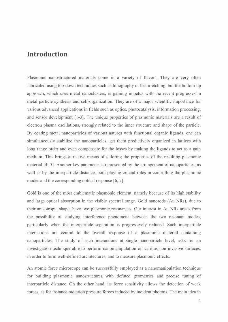
Plasmonic nanostructured materials come in a variety of flavors. They are very often
fabricated using top-down techniques such as lithography or beam-etching, but the bottom-up
approach, which uses metal nanoclusters, is gaining impetus with the recent progresses in
metal particle synthesis and self-organization. They are of a major scientific importance for
various advanced applications in fields such as optics, photocatalysis, information processing,
and sensor development [1 3]. The unique properties of plasmonic materials are a result of
electron plasma oscillations, strongly related to the inner structure and shape of the particle.
By coating metal nanoparticles of various natures with functional organic ligands, one can
simultaneously stabilize the nanoparticles, get them predictively organized in lattices with
long range order and even compensate for the losses by making the ligands to act as a gain
medium. This brings attractive means of tailoring the properties of the resulting plasmonic
material [4, 5]. Another key parameter is represented by the arrangement of nanoparticles, as
well as by the interparticle distance, both playing crucial roles in controlling the plasmonic
modes and the corresponding optical response [6, 7].
Gold is one of the most emblematic plasmonic element, namely because of its high stability
and large optical absorption in the visible spectral range. Gold nanorods (Au NRs), due to
their anisotropic shape, have two plasmonic resonances. Our interest in Au NRs arises from
the possibility of studying interference phenomena between the two resonant modes,
particularly when the interparticle separation is progressively reduced. Such interparticle
interactions are central to the overall response of a plasmonic material containing
nanoparticles. The study of such interactions at single nanoparticle level, asks for an
investigation technique able to perform nanomanipulation on various non-invasive surfaces,
in order to form well-defined architectures, and to measure plasmonic effects.
An atomic force microscope can be successfully employed as a nanomanipulation technique
for building plasmonic nanostructures with defined geometries and precise tuning of
interparticle distance. On the other hand, its force sensitivity allows the detection of weak
forces, as for instance radiation pressure forces induced by incident photons. The main idea in
2
this work was to use these two potentials of an AFM, in order to develop an optoelectronic
spectroscopy technique able to measure absorption effects of a finite number of particles with
tunable interparticle geometries.
AFM nanoparticle manipulation on surfaces requires, nevertheless, a good knowledge of
various interface processes usually captured by nanoscale friction experiments. A significant
part of this thesis was hence dedicated to understanding parameters relevant for nanoparticle
manipulation, while the ability of using the AFM as an optoelectronic spectroscopy technique
was subsequently explored.
The organization of the manuscript is the following: Chapter 1 briefly introduces the field of
plasmonic nanostructures, with an accent on the role of interparticle distance and organization
in the plasmonic effects. In Chapter 2, we discuss a few aspects related to the AFM
technique, as well as, the instrumental setup developed during this thesis. Chapter 3 and 4
present results obtained through nanoscale friction measurements on two types of surfaces,
namely on oxides surfaces and on CTAB molecular layers adsorbed on oxides. Chapter 5
presents findings gained during the nanomanipulation of CTAB-capped Au nanorods on oxide
surfaces. And, Chapter 6 includes our experimental and theoretical efforts to demonstrate the
feasibility of using an AFM as a force-based optoelectronic spectroscopy technique. The last
chapter summarizes the most important conclusions of our work and equally presents the
perspectives for further development and improvement of the AFM for detecting light
absorption spectra at the level of single nanoparticle.
3
References
[1] Y. Zhang, W. Chu, A. D. Foroushani, H. Wang, D. Li, J. Liu, C. J. Barrow, X. Wang and
W. Yang, "New Gold Nanostructures for Sensor Applications: A Review," Materials, vol.
7, p. 5169, 2014.
[2] M. Rahmani, T. Tahmasebi, Y. Lin, B. Lukiyanchuk, T. Y. F. Liew and M. H. Hong,
"Influence of plasmon destructive interferences on optical properties of gold planar
quadrumers," Nanotechnology, vol. 22, p. 245204, 2011.
[3] X. Zhang, X. Ke, A. Du and H. Zhu, "Plasmonic nanostructures to enhance catalytic
performance of zeolites under visible light," Scientific Reports, p. 3805, 2014.
[4] O. Kvítek, J. Siegel, V. Hnatowicz and V. Švorčík, "Noble metal nanostructures influence of structure and environment on their optical properties," Journal of Nanomaterials, p.
111, 2013.
[5] M. Hu, J. Chen, Z. -Y. Li, L. Au, G. V. Hartland, X. Li, M. Marquez and Y. Xia, "Gold
nanostructures: engineering their plasmonic properties for biomedical applications,"
Chemical Society Reviews, vol. 35, p. 1084, 2006.
[6] A. M. Funston, C. Novo, T. J. Davis and P. Mulvaney, "Plasmon coupling of gold
nanorods at short distances and in different geometries," Nano Letters, vol. 9, p. 1651,
2009.
[7] B. J. Reinhard, M. Siu, H. Agarwal, A. P. Alivisatos and J. Liphardt, "Calibration of
dynamic molecular rulers based on plasmon coupling between gold nanoparticles," Nano
Letters, vol. 5, p. 2246, 2005.

4

5
1 A brief introduction to plasmonic nanostructured
materials
When light interacts with some metallic structures, the external electromagnetic field induces
a collective oscillation of the conduction electrons. The frequency of oscillation depends on
several parameters, including the number of excited electrons (i.e., density of states at Fermi
level), electron-electron interactions, particle size and shape, but also external factors related
to the local environment and interparticle separation.
Depending on the type of object interacting with the electromagnetic radiation, two kinds of
plasmonic modes are distinguished, surface plasmon polaritons (SPPs), and localized surface
plasmons (LSPs) (see for instance [1]). SPPs are plasmonic excitations characteristic for
planar metal surfaces (e.g., metallic films, metal nanowires), characterized by dispersion in
energy, as they can propagate until their energy is either absorbed in the metal or dissipated.
LSP are the collective electronic oscillation occurring for particles with arbitrary geometries
(e.g., nanoparticles, nanorods), being non-propagating excitations.
The response of a metal nanoparticle subjected to an external electromagnetic field can be
determined through Mie’s theory, which represents solutions for Maxwell’s equations for
spherical particles [2, 3]. In the case of non-spherical particles (e.g., nanorods), a more
accurate analysis of the surface plasmon oscillation is given by the Gans modifications of the
Mie theory [4]. A shift in the surface plasmon resonance (SPR) occurs when the sphericity of
the particle is lost (electrons in boxes of different sizes). As a consequence, the longitudinal
and transversal dipole modes give different resonances. For a nanorod, this results in two
plasmon resonances: a red-shifted longitudinal plasmon resonance, corresponding to the long
axis of the nanorod, and a transversal one.

6
1.1 Role of interparticle distance and organization in
plasmonic response
The distance between nanoparticles has a great impact on frequency and amplitude of
plasmon resonances. Tuning particle spacing can induce, or not, near-field coupling effects,
which can be of different nature. In the case of a near-field coupling the resonance peak of
two interacting particles can red-shift [5], but new resonances at different frequencies may
also arise [6]. Besides the distance, the geometrical configuration is also crucial, particularly
in the case of anisotropic nanoparticles, like nanorods. Depending on the formed geometry
the coupling strength can vary, inducing shifts, amplitude variations, and generation of new
plasmonic modes (see for instance Figure 1.1). For spherical nanoparticles coupling effects
are usually seen as a blue-shift of existing resonances [7]. Nevertheless, the optical response
of the whole particulate system is very difficult to predict. This, again, asks for an
experimental technique able to change the nanoparticles positions and locally measure
absorption of light.
Figure 1.1. Example of simulated dipole formation and coupling for two interacting gold nanorods [6].
7
1.2 Exciton-plasmon coupling
Plasmons in nanoparticles suffer from intrinsic Landau and/or radiative damping, depending
on plasmon mode and frequency, proximity effects and particle size. The lost energy is either
transferred to phonons or dissipated through larger wavelength photons. This characteristic is
a serious issue for applications of plasmonic materials, since it triggers an increase of input
excitation light power, which is to be avoided because of ultimate heat it produces. Currently,
there is an emerging research field focusing on how to reduce the plasmonic damping in
plasmonic materials. A promising idea is to couple each plasmonic nanoparticle with discrete
level quantum systems, which can be molecules or semiconductor quantum dots.
Electron-hole pairs, called excitons can then transfer energy to mNPs, thus compensating at
least part of the inherent plasmon damping. The energy transfer mechanism depends on
various parameters, including distance, and can be recombination of the exciton and
subsequent absorption of the resulted photon by the plasmonic particle, radiationless Coulomb
dipole-dipole interaction, or the more striking quantum tunneling of electrons. As an example,
Zhao et al. reported on energy transfer between CdS QDs and AuNPs [8], while Li et al.
observed a distance-dependent enhancement effect of QDs-emission near AuNRs [9]. These
aspects can also be of a large importance in photochemistry, and upconverting systems (see
for instance [10]).
At the beginning of this thesis, we were also interested in revealing some collective plasmonic
properties. This was done in order to use the most promising nanoparticle systems for AFM
studies. The work has finally been focused on Au nanorods, but the role of interparticle
distance was revealed for two alternative systems based on spherical nanoparticles.
Figure 1.2 (a) shows spectra collected for solutions with different ratio Au NPs - QDs. Spectra
reveal a red-shift as the concentration of Au NPs increases. A picture on how these systems
can organize on a surface is shown in Figure 1.2 (b). The measured size of the particles
diameter was of 8±0.5 nm for Au NPs and 5±0.5 nm for QDs.

8
Figure 1.2. (a) UV-Vis extinction (absorption + diffusion) spectra showing a blue-shift for an increased
concentration of spherical [core-shell (CdSe)ZnS] QDs with respect to Au NPs. Spectra were collected for
solutions with an Agilent Cary 300 UV-Visible Spectrophotometer. (b) TEM image of Au NPs and QDs
assembled on a carbon amorphous surface. Dim particle are the QDs.
Other investigated systems were mixtures of Au NPs and fluorescein (C20H12O5), an organic
compound known as a dye. Figure 1.3 (a) shows the extinction spectra for a solution of Au
NPs while gradually increasing the concentration of fluorescein without changing
concentration of Au. In Figure 1.3 (b) the same measurement was performed, but with an
additional permanent UV irradiation at two different wavelengths.
Figure 1.3. (a) UV-Vis extinction spectra for Au NPs solutions with increasing concentration of
fluorescein. Black dashed arrow indicates the spectral response when increasing concentration of
fluorescein, while the red dashed arrow shows the intensity decrease of Au NPs spectral peak. (b) Similar
UV-Vis measurements, but under UV irradiation.
9
Both QDs and fluorescein induce a small blue-shift of Au NPs plasmonic resonance which
initially occurs around 530 nm, but most importantly the Au peak decreases in intensity,
indicating that less photons are absorbed, likely because of an energy transfer from QDs or
fluorescein, respectively. The effect enhances as the concentration of QDs or fluorescein
increases, as expected if the distance between the QDs, or fluorescein, decreases with respect
to the Au NPs. In the case of fluorescein, when adding additional excitations in the UV range
a red-shift can be observed, as well as a broadening of the Au NPs peak.

10
References
[1] S. A. Maier, Plasmonics: Fundamentals and Applications, Springer Science & Business
Media., 2007.
[2] G. Mie, "Beiträge zur Optik trüber Medien, speziell kolloidaler Metallösungen," Annalen
der Physik , p. 377, 1908.
[3] C. F. Bohrenn and D. R. Huffman, Absorption and Scattering by a Sphere, in Absorption
and Scattering of Light by Small Particles, Weinheim: Wiley-VCH Verlag GmbH, 2007.
[4] S. K. Ghosh and T. Pal, "Interparticle coupling effect on the surface plasmon resonance
of gold nanoparticles: From theory to applications," Chemical Reviews, vol. 107, p. 4797,
2007.
[5] K. -H. Su, Q. -H. Wei, X. Zhang, J. J. Mock, D. R. Smith and S. Schultz, "Interparticle
coupling effects on plasmon resonances of nanogold particles," Nanoletters, vol. 2003, p.
1087, 2003.
[6] A. M. Funston, C. Novo, T. J. Davis and P. Mulvaney, "Plasmon coupling of gold
nanorods at short distances and in different geometries," Nano Letters, vol. 9, p. 1651,
2009.
[7] W. Zhang, Q. Li and M. Qiu, "A plasmon ruler based on nanoscale photothermal effect,"
Optics Express, vol. 21, p. 172, 2013.
[8] W. -W. Zhao, J. Wang, J. -J. Xu and H. -Y. Chen, "Energy transfer between CdS
quantum dots and Au nanoparticles in photoelectrochemical detection," Chemical
Communications, vol. 47, p. 10990, 2011.
[9] X. Li, F. -J. Kao, C. -C. Chuang and S. He, "Enhancing fluorescence of quantum dots by
silica-coated gold nanorods under one- and two- photon excitation," Optics Express, vol.
18, p. 11335, 2010.
[10] S. Wu and H. -J. Butt, "Near-Infrared-Sensitive Materials Based on Upconverting
Nanoparticles," Advanced Materials, vol. 28, pp. 1208-1226, 2016.

11

12
2 Atomic force microscopy, nanotribology and
instrument development
2.1 Introduction
Since its invention, the atomic force microscope [1] has become a powerful and invaluable
tool for exploring phenomena arising from interactions at nanometer and atomic scale. Forces
of various origins - contact, electrostatic, magnetic, van der Waals, or even arising from
electromagnetic fluctuations - can be measured with an impressive precision on a very small
length scale. In the field of nanotribology, the AFM has been used to address complex
phenomena related to friction, adhesion, and wear, on a large variety of samples and
environments (see for instance [2]).
The friction force microscope was successfully employed for studying friction mechanisms as
a function of parameters, such as velocity [3 5], load [6 11], temperature [12 14], local
medium [15], or externally applied stimuli [16, 17]. These studies allowed a better
understanding of fundamental laws governing a sliding interface. More recently, improved
AFM techniques allow studying friction at sliding velocities up to 200 mm/s, thus entering the
range of operation of micro-/nanoelectromechanical devices [18].
The variation of friction force with normal load is a captivating characteristic, which has
generated lots of experimental and theoretic studies. Several friction regimes have been
revealed, including transitions from stick-slip to continuous sliding [19], linear to non-linear
friction variation [6], or ultralow friction [20, 21]. There are also very counterintuitive
behaviors of friction with load, such as friction increase when decreasing load (i.e., tip
retracting), due to particular adhesion effects [11].
The behavior of friction force with temperature is another fascinating point, central to the
dynamics of sliding interfaces. The Prandtl-Tomlinson model has thus been found to apply for
a large number of friction cases. However, the variation of friction with temperature also
13
demonstrated far more complex behaviors, including nonmonotonic behavior of friction with
temperature [12].
Likewise, various adhesion phenomena can be addressed by force measurements with an
AFM. Approach-retract force curves have therefore become a widespread approach for
addressing energetics of chemical bonds as well as conformational changes in molecular
systems, but also a number of mechanical characteristics of the sample, i.e. elastic modulus,
hardness, etc. (see for instance [22]).
Metal nanoparticles (mNPs) are becoming increasingly important in many fields. They are
nowadays studied in relation with an impressive number of properties. The extraordinary
success of mNPs is due to their high stability, achieved most of the time via protective organic
coatings. Complex chemical reactions are employed to this end, and this has attracted in the
last years more and more scientists from the chemistry community. Metal NPs became of a
huge interest in biology, medicine, pharmacology, and engineering. In physics, mNPs are
used for lubrication, sensors, switches, optics, etc.
The AFM is one of the main instrumentation tools for characterizing individual or groups of
particles. The nanotribology field also starts to benefit from the behavior of nanoparticles on
surfaces, through a controlled manipulation of well-defined nanoparticles of well-known sizes
and composition [23].
In general, AFM field is subject to a continuous development. This is, most of the time,
needed in order to enable specific measurements. In this chapter we also describe the
instrumental development realized throughout this thesis.
2.2 A brief description of an atomic force microscope
2.2.1 Principle of operation
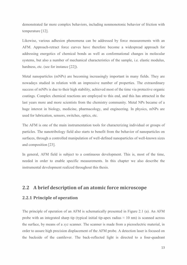
The principle of operation of an AFM is schematically presented in Figure 2.1 (a). An AFM
probe with an integrated sharp tip (typical initial tip-apex radius ≈ 10 nm) is scanned across
the surface, by means of a xyz scanner. The scanner is made from a piezoelectric material, in
order to assure high precision displacement of the AFM probe. A detection laser is focused on
the backside of the cantilever. The back-reflected light is directed to a four-quadrant
14
photodiode, which can measure the cantilever deflection. The deflection signal is defined by
(!"#)$(%"&)(!"#)"(%"&) [Figure 2.1 (a)]. This technique of measuring the cantilever deflection is also
known as an optical lever. Depending on tip – surface distance, the deflection can reveal
attractive or repulsive forces, which can originate from various interactions [Figure 2.1 (b)].
Figure 2.1. (a) Schematics of the basic operating principle of an AFM (not at scale). Detail on tip - surface
interaction. Depending on the distance between the tip and the surface, the forces contributing to the
cantilever deflection can be attractive (red double arrows) or repulsive (blue double arrows).
(c) Dominating forces in tip - surface interaction with respect to the distance between the tip and the
surface (adapted from [24]).
A general expressions of the equation of motion of the cantilever, which comprises most of
the interaction forces between a tip and a sample, can be written as: .
'*++ ,-.(/),/. 01'*++23 ,-(/),/ 01'*++43. -(/) = 156789*(/) 015:;<
015>?@AB?3 0158AB*7@CB8DA(,E FE GE HI) 0 57@6(/E HI) (2.1)
where meff is the effective mass of cantilever-tip probe, Γm the damping rate, Ωm the resonant
frequency, and x(t) is the deflection of the cantilever end with respect to its rest position. The
15
mechanical oscillator can be submitted to a sum of forces, originating from different sources
(right hand side of the equation). Fdrive represents the periodic driving force exerted by the
piezo. There are force terms inherently involved in the dynamics of probe, which apply no
matter if the AFM is operating in contact or non-contact mode, such as 5:;<, which is the
force rising from thermal fluctuations, and Fquantum which is given by electromagnetic
fluctuations (Casimir forces for instance). The magnitude of these two forces is quite small,
but can be important in some particular cases. The remaining force terms are Finteraction as
given by the tip – sample interaction, and which can depend on different external factors
(e.g., d – tip-sample distance, E – electric fields, B – magnetic fields, HI – photon energy)
and Frad the radiation force if photons are circulating between the tip and sample. To us, this
last force term was particularly important for exploring the capability of an AFM as an
absorption technique (see Chapter 6).
2.2.2 Tip – surface interactions
The local interaction between an AFM tip and a sample surface is governed by forces which
may have different origins. Particular AFM detection techniques are chosen in order to
separate this contribution by using their different variation as a function of distance. In Figure
2.1 (c) are summarized various interactions along with a rough estimation of tip-sample
distance employed for detection. This scale can be seen as the distance at which a specific
force has the largest importance when the tip gradually approaches a surface. There are
attractive, as well as repulsive forces. The impact of one or the other on probe deflection and
dynamics can be increased, or minimized, by using different methods. For instance,
equalizing the electrostatic potential between the tip and the sample can reduce the
electrostatic forces. Likewise, the absence of chemical bonds can be obtained by using
specific tips. Or, magnetic forces are eliminated by employing nonmagnetic tip. Nevertheless,
van der Waals forces are ubiquitous and usually seen as the main driving force for AFM
imaging.
In the attractive regime a van der Waals force between a tip and a surface can be
approximated as for a spherical particle near a flat surface by Equation 2.2 [25] :
596J(,) = 1KLMN,. (2.2)

16
where d represents the particle – surface distance, R is the radius of the particle, and AH is the
Hamaker constant, a material dependent factor. Van der Waals forces are the sum of three
contributions: (i) dipole-dipole interactions, also known as Keesom interactions,
(ii) dipole-induced dipole, or Debye induction, and (iii) dipole induced-dipole induce
interaction, known as London interactions. The last one have the most fundamental origin,
bringing the largest contribution to van der Waals forces.
Figure 2.2 highlights the range of the three AFM operation modes for imaging, with respect to
a tip – surface interaction potential, chosen here as a 2-8 Lennard-Jones potential: (i) contact
regime when the tip is at a distance of few angstroms from the surface, i.e., repulsive regime,
(ii) non-contact regime when the tip oscillation amplitude is smaller than the average tip
sample distance, and (iii) the intermittent (or dynamic) regime (tapping-modeÒ
of Bruker),
when the tip is alternatively brought into repulsive regime [26].
Figure 2.2. Interaction potential sensed by the probe, as a function of tip – surface distance, along with the
three AFM operation modes: contact mode, intermittent mode, and non-contact mode, respectively.
2.3 Instrumental setup
The apparatus shown in Figure 2.3 has been progressively developed and assembled during
this thesis. The AFM part is based on a commercial Bruker "enviroscope", which has been
modified at different levels. All the experiments presented in this dissertation were conducted
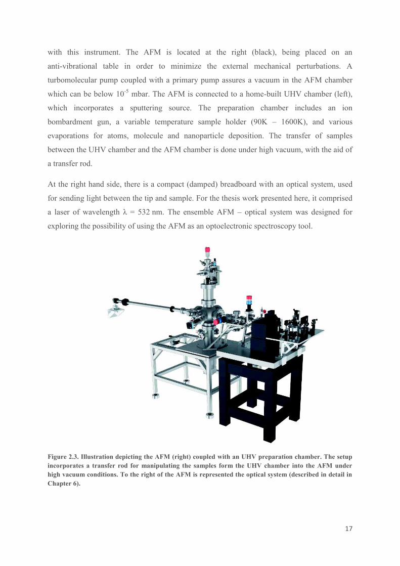
17
with this instrument. The AFM is located at the right (black), being placed on an
anti-vibrational table in order to minimize the external mechanical perturbations. A
turbomolecular pump coupled with a primary pump assures a vacuum in the AFM chamber
which can be below 10-5
mbar. The AFM is connected to a home-built UHV chamber (left),
which incorporates a sputtering source. The preparation chamber includes an ion
bombardment gun, a variable temperature sample holder (90K – 1600K), and various
evaporations for atoms, molecule and nanoparticle deposition. The transfer of samples
between the UHV chamber and the AFM chamber is done under high vacuum, with the aid of
a transfer rod.
At the right hand side, there is a compact (damped) breadboard with an optical system, used
for sending light between the tip and sample. For the thesis work presented here, it comprised
a laser of wavelength λ = 532 nm. The ensemble AFM – optical system was designed for
exploring the possibility of using the AFM as an optoelectronic spectroscopy tool.
Figure 2.3. Illustration depicting the AFM (right) coupled with an UHV preparation chamber. The setup
incorporates a transfer rod for manipulating the samples form the UHV chamber into the AFM under
high vacuum conditions. To the right of the AFM is represented the optical system (described in detail in
Chapter 6).
18
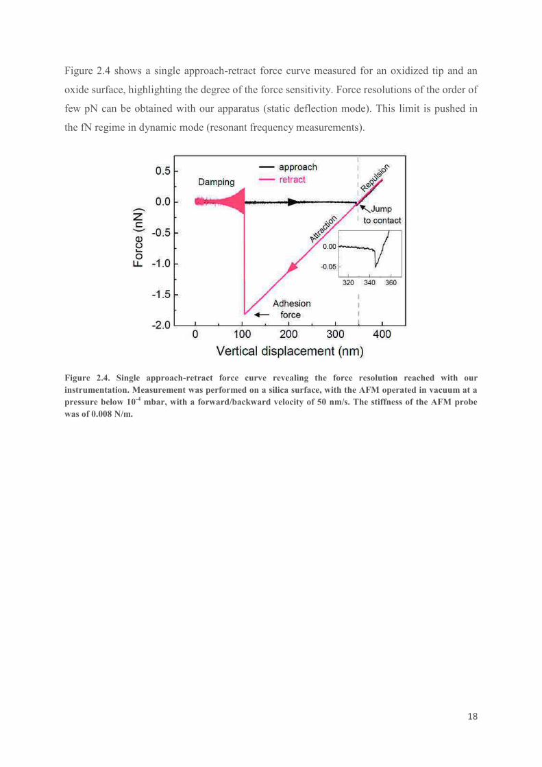
Figure 2.4 shows a single approach-retract force curve measured for an oxidized tip and an
oxide surface, highlighting the degree of the force sensitivity. Force resolutions of the order of
few pN can be obtained with our apparatus (static deflection mode). This limit is pushed in
the fN regime in dynamic mode (resonant frequency measurements).
Figure 2.4. Single approach-retract force curve revealing the force resolution reached with our
instrumentation. Measurement was performed on a silica surface, with the AFM operated in vacuum at a
pressure below 10-4
mbar, with a forward/backward velocity of 50 nm/s. The stiffness of the AFM probe
was of 0.008 N/m.

19
References
[1] G. Binnig, C. F. Quate and C. Gerber, "Atomic force microscope," Physical Review
Letters, vol. 56, p. 930, 1986.
[2] E. Gnecco and E. Meyer, Fundamentals of friction and wear, Berlin: Springer Berlin
Heidelberg, 2007.
[3] E. Gnecco, R. Bennewitz, T. Gyalog, C. Loppacher, M. Bammerlin, E. Meyer and H.-J.
Güntherodt, "Velocity dependence of atomic friction," Physical Review Letters, vol. 84,
p. 1172, 2000.
[4] R. W. Stark, G. Schitter and A. Stemmer, "Velocity dependent friction laws in contact
mode atomic force microscopy," Ultramicroscopy, vol. 100, p. 309, 2004.
[5] Y. Dong, H. Gao, A. Martini and P. Egberts, "Reinterpretation of velocity-dependent
atomic friction: Influence of the inherent instrumental noise in friction force
microscopes," Physical Review E, vol. 90, p. 012125, 2014.
[6] J. Hu, X. -d. Xiao, D. F. Ogletree and M. Salmeron, "Atomic scale friction and wear of
mica," Surface Science, vol. 327, p. 358, 1995.
[7] S. Fujisawa, E. Kishi, Y. Sugawara and S. Morita, "Load dependence of two-dimensional
atomic-scale friction," Physical Review B, vol. 52, p. 5302, 1995.
[8] U. D. Schwarz, O. Zwörner, P. Köster and R. Wiesendanger, "Quantitative analysis of the frictional properties of solid materials at low loads. I. Carbon compounds," Physical
Review B, vol. 56, p. 6987, 1997.
[9] S. Fujisawa, "Analysis of experimental load dependence of two-dimensional atomic-
scale friction," Physical Review B, vol. 58, p. 4909, 1998.
[10] Y. Mo, K. T. Turner and I. Szlufarska, "Friction laws at the nanoscale," Nature, vol. 457,
p. 1116, 2009.
[11] Z. Deng, A. Smolyanitsky, Q. Li, X. Feng and R. J. Cannara, "Adhesion-dependent
negative friction coefficient on chemically modified graphite at the nanoscale," Nature
Materials, vol. 11, p. 1032, 2012.
[12] A. Schirmeisen, L. Jansen, H. Hölscher and H. Fuchs, "Temperature dependence of point contact friction on silicon," Applied Physics Letters, vol. 88, p. 123108, 2006.
20
[13] Q. Liang, H. Li, Y. Xu and X. Xiao, "Friction and adhesion between C60 single crystal
surfaces and AFM tips: Effects of the orientational phase transition," Journal of Physical
Chemistry B, vol. 110, p. 403, 2006.
[14] C. Greiner, J. R. Felts, Z. Dai, W. P. King and R. W. Carpick, "Temperature dependence
of nanoscale friction investigated with thermal AFM probes," Mechanochemistry in
Materials Science, vol. 1226, p. 13, 2010.
[15] R. Lüthi, E. Meyer, M. Bammerlin, L. Howald, T. Lehmann, C. Loppacher and H. -J.
Güntherodt, "Friction on the atomic scale: An ultrahigh vacuum atomic force microscopy
study on ionic crystals," Journal of Vacuum Science & Technology B, Nanotechnology
and Microelectronics: Materials, Processing, Measurement, and Phenomena, vol. 14, p.
1280, 2016.
[16] K. S. Karuppiah, Y. Zhou, L. K. Woo and S. Sundararajan, "Nanoscale friction switches:
friction modulation of monomolecular assemblies using external electric fields,"
Langmuir, vol. 25, p. 12114, 2009.
[17] G. Conache, A. Ribayrol, L. E. Fröberg, M. T. Borgström, L. Samuelson, L. Montelius, H. Pettersson and S. M. Gray, "Bias-controlled friction of InAs nanowires on a silicon
nitride layer studied by atomic force microscopy," Physical Review B, vol. 82, p. 035403,
2010.
[18] Z. Tao and B. Bhushan, "New technique for studying nanoscale friction at sliding
velocities up to 200 mm/s using atomic force microscope," Review of Scientific
Instruments, vol. 77, p. 103705, 2016.
[19] H. Hölscher, A. Schirmeisen and U. D. Schwarz, "Principles of atomic friction: from
sticking atoms to superlubric sliding," Philosophical Transactions of the Royal Society A,
vol. 366, p. 1383, 2008.
[20] A. Socoliuc, R. Bennewitz, E. Gnecco and E. Meyer, "Transition from stick-slip to
continuous sliding in atomic friction: Entering a new regime of ultralow friction,"
Physical Review Letters, vol. 92, p. 134301, 2004.
[21] D. Dietzel, M. Feldmann, U. D. Schwarz, H. Fuchs and A. Schirmeisen, "Scaling laws of
structural lubricity," Physical Review Letters, vol. 111, p. 235502, 2013.
[22] H.-J. Butt, B. Cappella and M. Kappl, "Force measurements with the atomic force
microscope: Technique, interpretation and applications," Surface Science Reports, vol.
59, pp. 1-152, 2005.
[23] A. Schirmeisen and U. D. Schwarz, "Measuring the friction of nanoparticles: a new route
towards a better understanding of nanoscale friction," ChemPhysChem, vol. 10, p. 2373,
2009.

21
[24] Nanoscience, "Scanning Probe Methods Group," 2017. [Online]. Available:
http://www.nanoscience.de/HTML/methods/afm.html.
[25] J. N. Israelachvili, Intermolecular and surface forces, 3rd ed., Academic Press, 2011.
[26] J. Sharpe and N. William, Eds., Springer Handbook of Experimental Solid Mechanics,
Springer Science & Business Media, 2008.
[27] M. Aspelmeyer, T. Kippenberg and F. Marquardt, "Cavity optomechanics," Review of
Modern Physics, vol. 86, p. 1391, 2014.
[28] R. Ferencz, J. Sanchez, B. Blümich and W. Herrmann, "AFM nanoindentation to determine Young’s modulus for different EPDM elastomers," Polymer Testing , vol. 31,
p. 425, 2012.

22
23
3 Friction and adhesion at nanoscale interfaces
3.1 Introduction
A good knowledge on interface interactions between an AFM probe and a nanoparticle (NP),
or between a NP and a substrate is highly important for nanomanipulation processes. Our
focus here is on interface interactions which may govern a NP displacement on a particular
surface. Oxide dielectric surfaces appeared to us as a good choice because they present a low
density of electrons, ensuring a good preservation of electronic and optical properties of metal
NPs.
We addressed the NP-oxide surface interaction from two different perspectives. The first one
constitutes the subject of this chapter, and is based on the idea that unfunctionalized NPs have
to be manipulated. In this case, the nanoscale sliding properties have been studied by
analyzing the friction and adhesion characteristics of an AFM tip on various oxide surfaces.
This type of contact is similar to what occurs for supported nanoparticles, when no organic
ligands are used. The second perspective concerns the interface between a functionalized
nanoparticle and an oxide substrate, and is treated in the next chapter.
We studied friction and adhesion on various oxide surfaces conducted with a silicon oxide.
Results revealed a stick-slip nanoscale friction mechanism which appears to be a common
characteristic for all oxide surfaces investigated here, and which, to our knowledge, has never
been reported before.
3.2 Stick-slip friction on oxide surfaces
Stick-slip friction is a prime example of energy conversion and dissipation at many length
scales (see for instance [1]). At atomic level, atoms move on crystalline surfaces by a
thermally assisted stick-slip friction mechanism [2]. At larger scales, effects such as creaking
doors, screeching brakes, or the sounds of bowed instruments and grasshoppers are generated

24
by stick-slip movements. However, the stick phases of nanometer lengths are very rarely
observed [3 7]. Overall, a stick-slip process occurs when momentum is transferred to an
elastic portion of a sliding body, and then at least part of the stored potential elastic energy is
released. To fulfill this condition the force gradient of the stretched contact must be at a given
moment greater than the pulling force constant [8, 9]. Despite this knowledge drawn from
atomic friction, it remains difficult to predict why stick-slip motion is so unpopular at the
nanoscale. Several friction models based on the Prandtl – Tomlinson (PT) approach [10, 11]
have been proposed to interpret experiments conducted with atomic scale asperities [12 15].
However, these models use the atomic potentials of crystalline surfaces, in contrast with most
practical sliding surfaces which are covered by amorphous oxides [16 18].
3.3 AFM experiments
3.3.1 Experimental details
The friction measurements described in this chapter were performed with an atomic force
microscope (AFM) operating below 10−4
mbar and at various temperatures. All samples were
outgassed in vacuum for several hours. The samples were checked for cleanliness by
approach – retract force curves. With the sharpest tips, we found adhesion forces between
2 and 3 nN, which indicate the absence of chemical bonds and of water capillary effects.
Friction data were gathered by recording the lateral friction force signal while scanning
perpendicularly to the cantilever axis. We used silicon probes with original tip radii of about
10 nm. Subsequent electron microscopy analyses revealed that the probes were not affected
by our friction experiments. The normal and lateral spring constants of the probes were of the
order of 0.01 and 20 N/m, respectively. Stiffer probes or ambient conditions are both
detrimental to a clear observation of stick-slip phases.
3.3.2 Friction and adhesion measurements
We performed friction measurements on various oxide surfaces, such as: silicon surface with
a native oxide layer thickness of 200 nm and of 3 nm, alumina surface, and glass surface. In
Figure 3.1 (a) we present a forward friction image recorded on a silica surface where it can be
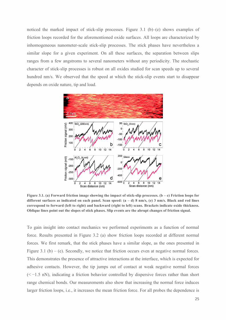
25
noticed the marked impact of stick-slip processes. Figure 3.1 (b)–(e) shows examples of
friction loops recorded for the aforementioned oxide surfaces. All loops are characterized by
inhomogeneous nanometer-scale stick-slip processes. The stick phases have nevertheless a
similar slope for a given experiment. On all these surfaces, the separation between slips
ranges from a few angstroms to several nanometers without any periodicity. The stochastic
character of stick-slip processes is robust on all oxides studied for scan speeds up to several
hundred nm/s. We observed that the speed at which the stick-slip events start to disappear
depends on oxide nature, tip and load.
Figure 3.1. (a) Forward friction image showing the impact of stick-slip processes. (b – e) Friction loops for
different surfaces as indicated on each panel. Scan speed: (a – d) 8 nm/s, (e) 3 nm/s. Black and red lines
correspond to forward (left to right) and backward (right to left) scans. Brackets indicate oxide thickness.
Oblique lines point out the slopes of stick phases. Slip events are the abrupt changes of friction signal.
To gain insight into contact mechanics we performed experiments as a function of normal
force. Results presented in Figure 3.2 (a) show friction loops recorded at different normal
forces. We first remark, that the stick phases have a similar slope, as the ones presented in
Figure 3.1 (b) – (e). Secondly, we notice that friction occurs even at negative normal forces.
This demonstrates the presence of attractive interactions at the interface, which is expected for
adhesive contacts. However, the tip jumps out of contact at weak negative normal forces
(< −1.5 nN), indicating a friction behavior controlled by dispersive forces rather than short
range chemical bonds. Our measurements also show that increasing the normal force induces
larger friction loops, i.e., it increases the mean friction force. For all probes the dependence is
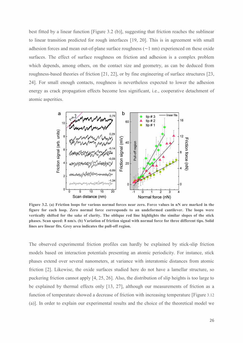
26
best fitted by a linear function [Figure 3.2 (b)], suggesting that friction reaches the sublinear
to linear transition predicted for rough interfaces [19, 20]. This is in agreement with small
adhesion forces and mean out-of-plane surface roughness (O1 nm) experienced on these oxide
surfaces. The effect of surface roughness on friction and adhesion is a complex problem
which depends, among others, on the contact size and geometry, as can be deduced from
roughness-based theories of friction [21, 22], or by fine engineering of surface structures [23,
24]. For small enough contacts, roughness is nevertheless expected to lower the adhesion
energy as crack propagation effects become less significant, i.e., cooperative detachment of
atomic asperities.
Figure 3.2. (a) Friction loops for various normal forces near zero. Force values in nN are marked in the
figure for each loop. Zero normal force corresponds to an undeformed cantilever. The loops were
vertically shifted for the sake of clarity. The oblique red line highlights the similar slopes of the stick
phases. Scan speed: 8 nm/s. (b) Variation of friction signal with normal force for three different tips. Solid
lines are linear fits. Grey area indicates the pull-off region.
The observed experimental friction profiles can hardly be explained by stick-slip friction
models based on interaction potentials presenting an atomic periodicity. For instance, stick
phases extend over several nanometers, at variance with interatomic distances from atomic
friction [2]. Likewise, the oxide surfaces studied here do not have a lamellar structure, so
puckering friction cannot apply [4, 25, 26]. Also, the distribution of slip heights is too large to
be explained by thermal effects only [13, 27], although our measurements of friction as a
function of temperature showed a decrease of friction with increasing temperature [Figure 3.12
(a)]. In order to explain our experimental results and the choice of the theoretical model we
27
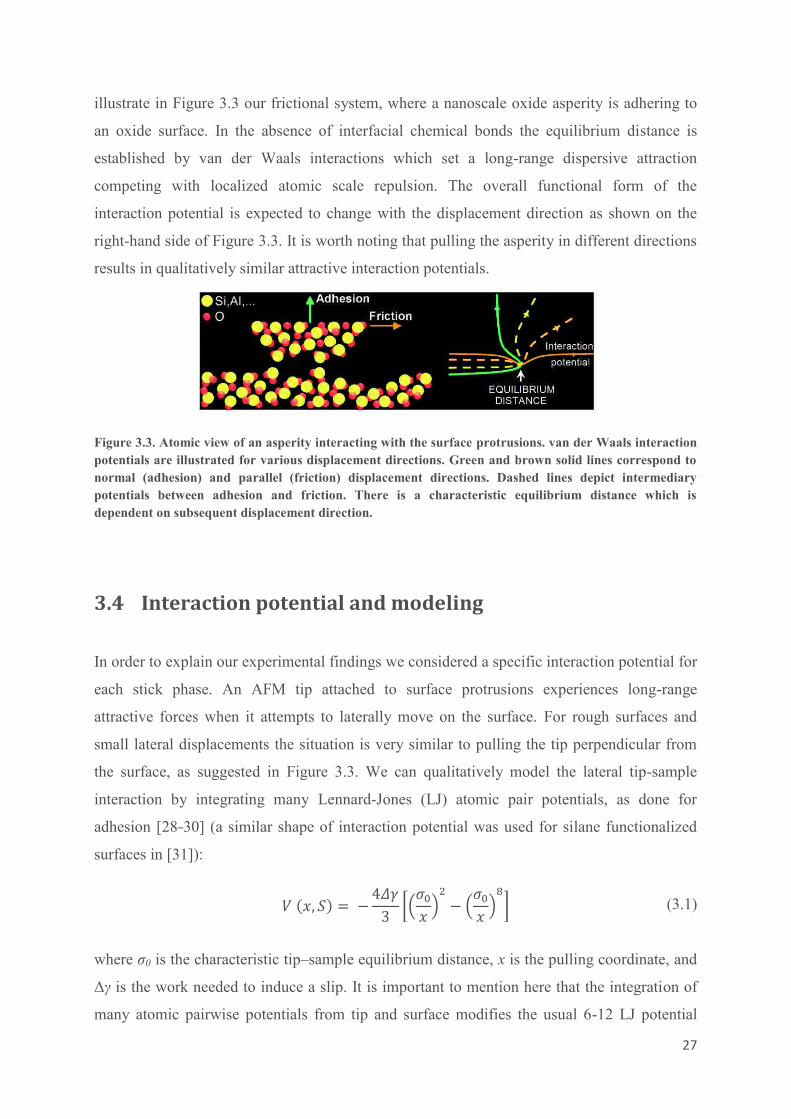
illustrate in Figure 3.3 our frictional system, where a nanoscale oxide asperity is adhering to
an oxide surface. In the absence of interfacial chemical bonds the equilibrium distance is
established by van der Waals interactions which set a long-range dispersive attraction
competing with localized atomic scale repulsion. The overall functional form of the
interaction potential is expected to change with the displacement direction as shown on the
right-hand side of Figure 3.3. It is worth noting that pulling the asperity in different directions
results in qualitatively similar attractive interaction potentials.
Figure 3.3. Atomic view of an asperity interacting with the surface protrusions. van der Waals interaction
potentials are illustrated for various displacement directions. Green and brown solid lines correspond to
normal (adhesion) and parallel (friction) displacement directions. Dashed lines depict intermediary
potentials between adhesion and friction. There is a characteristic equilibrium distance which is
dependent on subsequent displacement direction.
3.4 Interaction potential and modeling
In order to explain our experimental findings we considered a specific interaction potential for
each stick phase. An AFM tip attached to surface protrusions experiences long-range
attractive forces when it attempts to laterally move on the surface. For rough surfaces and
small lateral displacements the situation is very similar to pulling the tip perpendicular from
the surface, as suggested in Figure 3.3. We can qualitatively model the lateral tip-sample
interaction by integrating many Lennard-Jones (LJ) atomic pair potentials, as done for
adhesion [28 30] (a similar shape of interaction potential was used for silane functionalized
surfaces in [31]):
! P1(-E Q) = 1RSTUV WXYZ- [. R XYZ- [
\]! (3.1)
where σ0 is the characteristic tip–sample equilibrium distance, x is the pulling coordinate, and
Δγ is the work needed to induce a slip. It is important to mention here that the integration of
many atomic pairwise potentials from tip and surface modifies the usual 6-12 LJ potential
28
(typical for atomic and molecular interactions) in a 2-8 functional form, as observed in
Equation 3.1. This translates into larger distance-dependent attractive and repulsive regimes.
For rough tips and surfaces, when the contact is likely established through asperities, Δγ can
be approximated by adhesive energy. This is a parameter which scales with the contact
surface and is a priori known for a given material. For numerical modeling we took
1 × 10⁻¹⁹
J/nm2 (we used Δγ = γ1 + γ2 with γ1 = γ2 ≈ 50 mJ/m
2 the surface energy of tip and
sample, and neglect interface energy; the values were employed from the work of
Maugis D. [32]). Thus, Δγ depends on effective contact surface S, which we allow to vary
after a slip. This, again, is expected because of the amorphous and rough character of both tip
and surface. Our reasoning is in line with a recent work of Mo et al. [19], where the contact is
considered as discontinuous across the interface. In our model we also considered a
cooperative unbounding of many asperities at the stick–slip transition and a rebounding after
the slip event, processes encountered for instance in frictional molecular junctions [33]. The
interface lateral forces were calculated along the sliding direction from the gradient of the
interaction potential:
! 51(-E Q) = ^P1(-E Q) ^-_ ! (3.2)
Figure 3.4 (a) shows the interaction potential plotted considering four different contact
surfaces, S1 = 4 nm2, S2 = 6.9 nm
2, S3 = 10 nm
2, and S4 = 15 nm
2. By deriving this interaction
potential we obtain the surface force exerted on the tip, i.e., the interface lateral force, for each
contact surface S. The F(x) curves are shown in Figure 3.4 (b). Similar to atomic friction,
combining F with the linear pulling force of the probe115̀ = 1Ra`-, where kp = 20 N/m is our
experimental torsional spring constant, provides information on sliding dynamics. For
instance, when kp is higher than the curvature of the interaction gradient at its maximum
^51(-E Q)b^- (i.e., maximum contact stiffness kc, red segments in Figure 3.4), the total
probe-surface potential defines one stable position.

29
Figure 3.4. (a) Interaction potentials V (x, S) plotted for various contact surfaces S. (b) Interface lateral
forces (solid curves) calculated from the gradient of V (x, S) presented in (a). The dashed curve shows, as
an example, V(x) for S1 = 4 nm2. The sloped straight lines trace the linear pulling force taken with a
negative sign for various positions of the probe. The blue dots mark the intersections between the pulling
forces with the interface forces, which represent the stable positions for the tip. Red segments depict the
maximum curvature of the interface force, i.e., contact stiffness kc.
This case is illustrated in Figure 3.4 (b) for S1. As the probe moves, the tip then follows this
stable contact state, which results in a continuous sliding. Conversely, each time S increases
above a critical value (for our kp we find S2 = 6.9 nm2) the total potential presents two stable
states, which initiates a stick-slip sliding. A graphical solution to this case is shown in Figure
3.4 (b) for S3 and S4.
Two sliding regimes are then defined by the relationship between S and kp, as shown in Figure
3.5. At c = d1e, for any combination of S and kp which falls into the stick-slip regime, the tip
remains into the initial bound state until the probe sufficiently advances to the right and
reaches a critical point xc, when the tip performs a sudden transition into the second state.
Figure 3.5. Two sliding regimes defined by the relationship between S and kp.
30
Similar to atomic [12] and puckering [4] friction, at T ≠ 0 K, a thermally activated transition is
expected well before the probe reaches xc. Moreover, for some intermediate probe
displacements the tip can transit back and forth between the two states. Nevertheless, as the
probe moves further, the time needed to thermally activate a back transition increases, making
such a transition more unlikely. Hence, at high enough speeds the tip performs a single
forward transition for each stick phase [slips in Figure 3.1 (b – e) and Figure 3.2 (a)]. These
aspects will be discussed in detail in the following section, where several situations defining
tip – sample interaction will be presented.
3.4.1 Dynamics of sliding mechanics
In order to investigate the dynamics of the friction mechanism we have simulated the
potential described by a tip – sample interaction for a variety of situations, from a single
contact position, to multiple contacts between the tip and the surface. Simulation data of the
evolution of total potential as a function of probe displacement are presented below and
represents a visual support for the proposed model, contributing to a better understanding of
the formation and fluctuation of the stick-slip phases. For all simulated potential we
considered a probe stiffness kp = 20 N/m, as experimentally used. In a first instance we
present in Figure 3.6 how we have obtained the simulated data, highlighting in the same the
parameters important when discussing sliding dynamics.

31
Figure 3.6. (a) Interaction potentials for a contact surface S = 15 nm2. Black line (fg") shows the
interaction potential for a right sliding coordinate, while red line (fg$) corresponds to a left sliding
coordinate. (b) Surface interaction potential (black curve) obtained by summing up attractive parts of the
potential from (a). The green curve represents the quadratic potential of the probe. Total interaction
potential (orange curve) is obtained by combining surface potential with the quadratic potential. xp
designates the probe displacement. (c) and (d) depict the evolution of total interaction potential when
displacing the probe towards the left (c) or towards the right (d) for a distance of 0.3 nm.
Using Equation 3.1 we simulated the interaction potentials considering a contact surface of
15 nm2 [Figure 3.6 (a)]. By summing up the attractive parts of the potential from (a) we
obtained the surface interaction potential [black curve in Figure 3.6 (b)]. Combining the
surface potential with the quadratic potential of the probe [green curve in Figure 3.6 (b)] we
obtained a total interaction potential sensed by the tip. The evolution of this potential is
illustrated for a probe displacement xp = 0.3 nm to the left or to the right [orange curve in
Figure 3.6 (c), (d)].
The two next cases (Figure 3.7 and Figure 3.8) highlight the importance of contact surface S
in determining the type of sliding regime. In Figure 3.7 surface potential was calculated for
S = 4 nm2. In this situation, as kp is higher than kc, the total potential will define only one
stable position, thus when the probe is displaced towards the right, the tip experiences
continuously sliding.
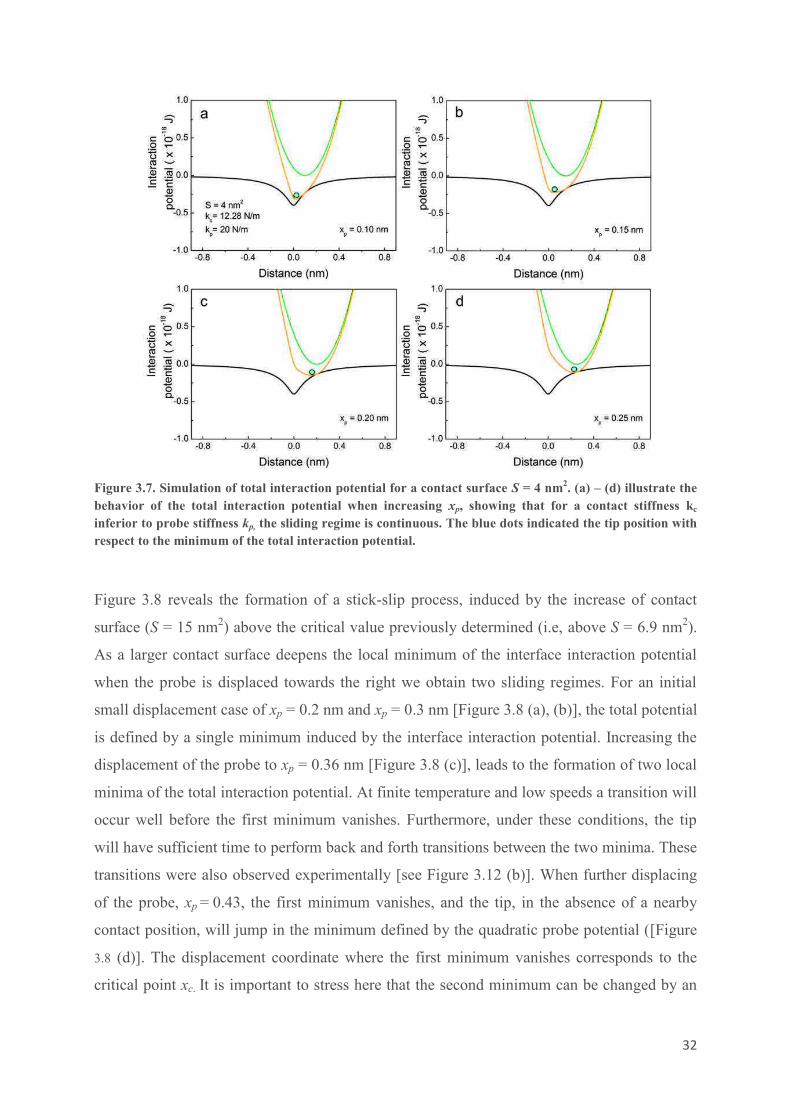
32
Figure 3.7. Simulation of total interaction potential for a contact surface S = 4 nm2. (a) – (d) illustrate the
behavior of the total interaction potential when increasing xp, showing that for a contact stiffness kc
inferior to probe stiffness kp, the sliding regime is continuous. The blue dots indicated the tip position with
respect to the minimum of the total interaction potential.
Figure 3.8 reveals the formation of a stick-slip process, induced by the increase of contact
surface (S = 15 nm2) above the critical value previously determined (i.e, above S = 6.9 nm
2).
As a larger contact surface deepens the local minimum of the interface interaction potential
when the probe is displaced towards the right we obtain two sliding regimes. For an initial
small displacement case of xp = 0.2 nm and xp = 0.3 nm [Figure 3.8 (a), (b)], the total potential
is defined by a single minimum induced by the interface interaction potential. Increasing the
displacement of the probe to xp = 0.36 nm [Figure 3.8 (c)], leads to the formation of two local
minima of the total interaction potential. At finite temperature and low speeds a transition will
occur well before the first minimum vanishes. Furthermore, under these conditions, the tip
will have sufficient time to perform back and forth transitions between the two minima. These
transitions were also observed experimentally [see Figure 3.12 (b)]. When further displacing
of the probe, xp = 0.43, the first minimum vanishes, and the tip, in the absence of a nearby
contact position, will jump in the minimum defined by the quadratic probe potential ([Figure
3.8 (d)]. The displacement coordinate where the first minimum vanishes corresponds to the
critical point xc. It is important to stress here that the second minimum can be changed by an
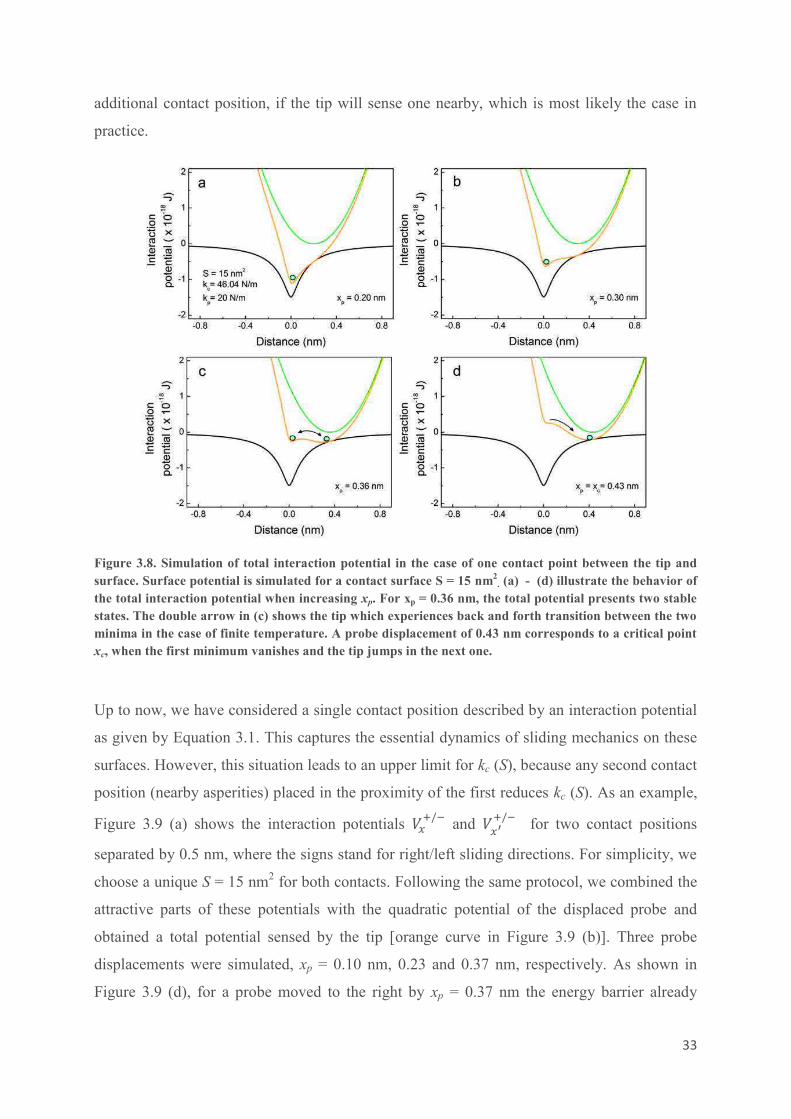
33
additional contact position, if the tip will sense one nearby, which is most likely the case in
practice.
Figure 3.8. Simulation of total interaction potential in the case of one contact point between the tip and
surface. Surface potential is simulated for a contact surface S = 15 nm2
. (a) - (d) illustrate the behavior of
the total interaction potential when increasing xp. For xp = 0.36 nm, the total potential presents two stable
states. The double arrow in (c) shows the tip which experiences back and forth transition between the two
minima in the case of finite temperature. A probe displacement of 0.43 nm corresponds to a critical point
xc, when the first minimum vanishes and the tip jumps in the next one.
Up to now, we have considered a single contact position described by an interaction potential
as given by Equation 3.1. This captures the essential dynamics of sliding mechanics on these
surfaces. However, this situation leads to an upper limit for kc (S), because any second contact
position (nearby asperities) placed in the proximity of the first reduces kc (S). As an example,
Figure 3.9 (a) shows the interaction potentials Ph"b$ and Phi"b$ for two contact positions
separated by 0.5 nm, where the signs stand for right/left sliding directions. For simplicity, we
choose a unique S = 15 nm2 for both contacts. Following the same protocol, we combined the
attractive parts of these potentials with the quadratic potential of the displaced probe and
obtained a total potential sensed by the tip [orange curve in Figure 3.9 (b)]. Three probe
displacements were simulated, xp = 0.10 nm, 0.23 and 0.37 nm, respectively. As shown in
Figure 3.9 (d), for a probe moved to the right by xp = 0.37 nm the energy barrier already
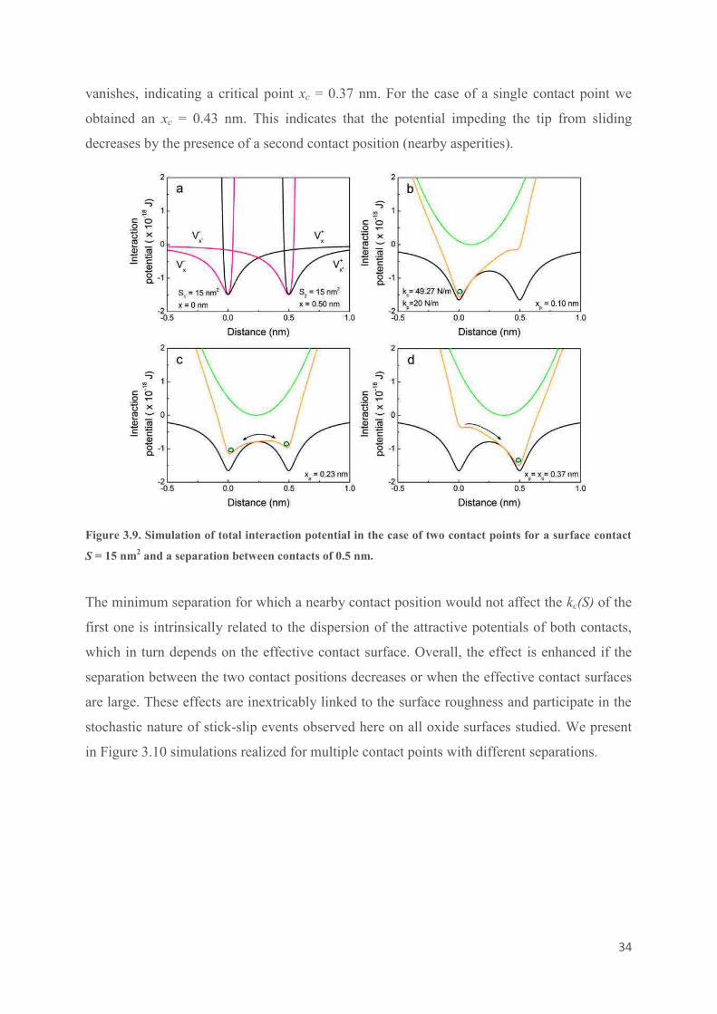
34
vanishes, indicating a critical point xc = 0.37 nm. For the case of a single contact point we
obtained an xc = 0.43 nm. This indicates that the potential impeding the tip from sliding
decreases by the presence of a second contact position (nearby asperities).
Figure 3.9. Simulation of total interaction potential in the case of two contact points for a surface contact
S = 15 nm2 and a separation between contacts of 0.5 nm.
The minimum separation for which a nearby contact position would not affect the kc(S) of the
first one is intrinsically related to the dispersion of the attractive potentials of both contacts,
which in turn depends on the effective contact surface. Overall, the effect is enhanced if the
separation between the two contact positions decreases or when the effective contact surfaces
are large. These effects are inextricably linked to the surface roughness and participate in the
stochastic nature of stick-slip events observed here on all oxide surfaces studied. We present
in Figure 3.10 simulations realized for multiple contact points with different separations.

35
Figure 3.10. Evolution of total potential as a function of probe displacement in the case of successive
contact points with various contact surfaces and separation distances.
36
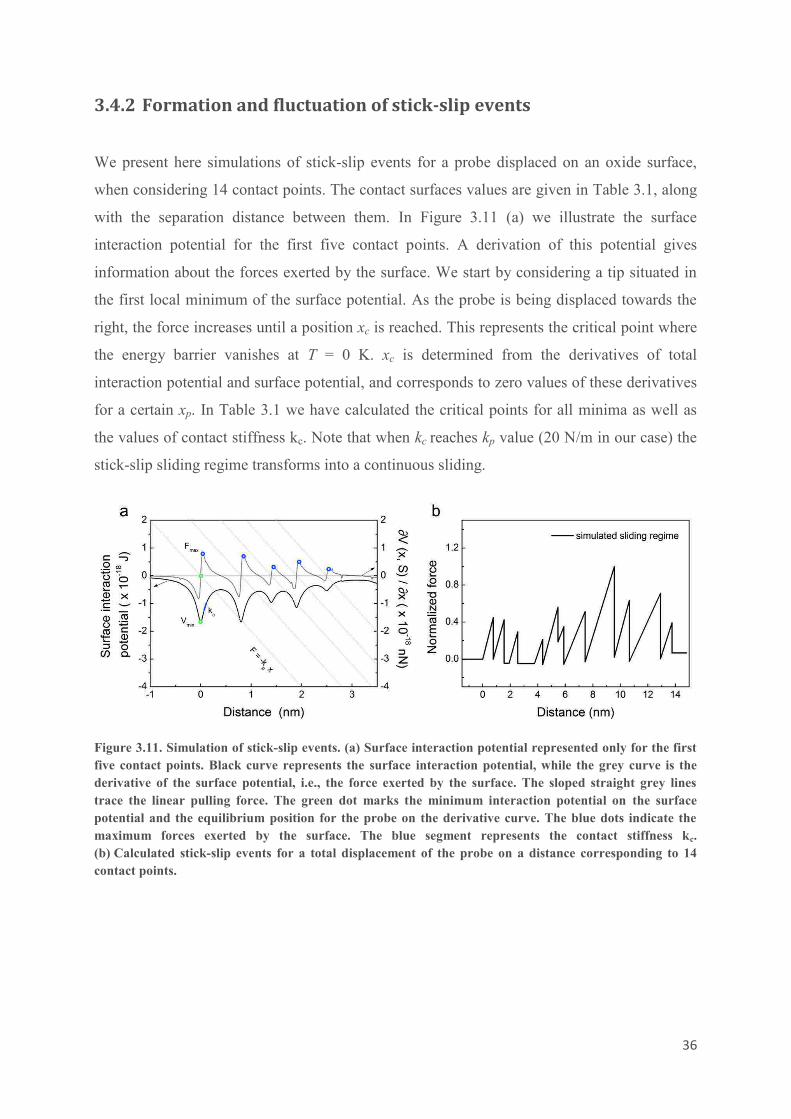
3.4.2 Formation and fluctuation of stick-slip events
We present here simulations of stick-slip events for a probe displaced on an oxide surface,
when considering 14 contact points. The contact surfaces values are given in Table 3.1, along
with the separation distance between them. In Figure 3.11 (a) we illustrate the surface
interaction potential for the first five contact points. A derivation of this potential gives
information about the forces exerted by the surface. We start by considering a tip situated in
the first local minimum of the surface potential. As the probe is being displaced towards the
right, the force increases until a position xc is reached. This represents the critical point where
the energy barrier vanishes at T = 0 K. xc is determined from the derivatives of total
interaction potential and surface potential, and corresponds to zero values of these derivatives
for a certain xp. In Table 3.1 we have calculated the critical points for all minima as well as
the values of contact stiffness kc. Note that when kc reaches kp value (20 N/m in our case) the
stick-slip sliding regime transforms into a continuous sliding.
Figure 3.11. Simulation of stick-slip events. (a) Surface interaction potential represented only for the first
five contact points. Black curve represents the surface interaction potential, while the grey curve is the
derivative of the surface potential, i.e., the force exerted by the surface. The sloped straight grey lines
trace the linear pulling force. The green dot marks the minimum interaction potential on the surface
potential and the equilibrium position for the probe on the derivative curve. The blue dots indicate the
maximum forces exerted by the surface. The blue segment represents the contact stiffness kc.
(b) Calculated stick-slip events for a total displacement of the probe on a distance corresponding to 14
contact points.
37
Table 3.1. Parameters S and xp used for the simulation of a surface potential interaction formed by 14
contact points. Contact stiffness values (kc) and critical point values (xc) extracted from simulation are also
presented.
S
(nm2)16 15 6.9 10 4 8 20 12 18 35 22 25 14 6.9
xp
(nm)0 0.8 1.4 1.9 2.5 3.8 4.6 5.2 6.6 8.3 9.7 11.9 13.0 13.5
kc
(N/m)49.79 47.38 24.26 31.89 12.96 25.53 62.99 38.03 55.43 107.59 67.67 76.95 44.67 22.45
xc
(nm)0.42 1.22 - 2.20 - 4.04 5.14 5.56 7.1 9.2 10.3 12.56 13.38 -
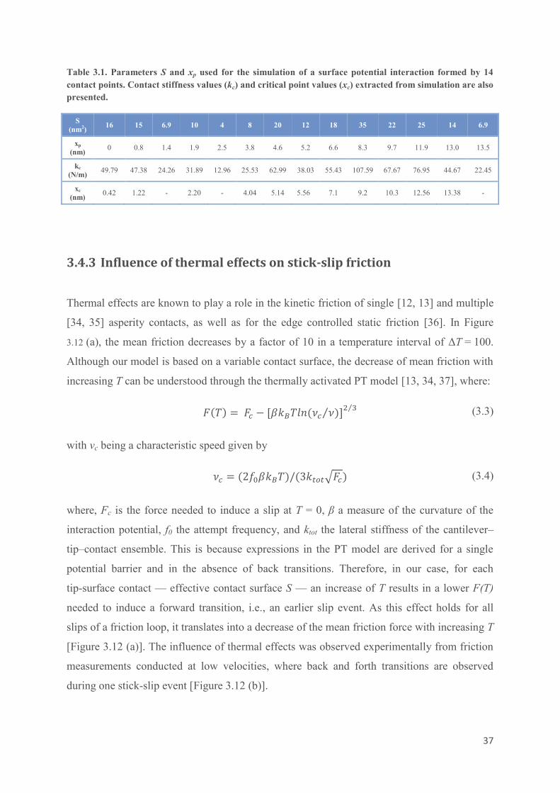
3.4.3 Influence of thermal effects on stick-slip friction
Thermal effects are known to play a role in the kinetic friction of single [12, 13] and multiple
[34, 35] asperity contacts, as well as for the edge controlled static friction [36]. In Figure
3.12 (a), the mean friction decreases by a factor of 10 in a temperature interval of ΔT = 100.
Although our model is based on a variable contact surface, the decrease of mean friction with
increasing T can be understood through the thermally activated PT model [13, 34, 37], where:
5(c) = 15C R jka#clm(nC n)o_ . p_ (3.3)
with νc being a characteristic speed given by
nC = (qrZka#c)b(VaBDBs5C) (3.4)
where, Fc is the force needed to induce a slip at T = 0, β a measure of the curvature of the
interaction potential, f0 the attempt frequency, and ktot the lateral stiffness of the cantilever–
tip–contact ensemble. This is because expressions in the PT model are derived for a single
potential barrier and in the absence of back transitions. Therefore, in our case, for each
tip-surface contact — effective contact surface S — an increase of T results in a lower F(T)
needed to induce a forward transition, i.e., an earlier slip event. As this effect holds for all
slips of a friction loop, it translates into a decrease of the mean friction force with increasing T
[Figure 3.12 (a)]. The influence of thermal effects was observed experimentally from friction
measurements conducted at low velocities, where back and forth transitions are observed
during one stick-slip event [Figure 3.12 (b)].
38
Figure 3.12. (a) Experimental variation of mean friction signal with temperature. (b) Forwards (black)
and backward (red) friction profiles showing back and forth tip transitions. Scan speed: 0.5 nm/s,
T = 300 K.
It is also interesting to note that for any damped system close to a transition point both f0 and
β depend on (^pPb^-p)t ._ [13]. As V(x) is in our case a function of S, slips are expected to
occur at different f0 and β values. This is again at variance with the majority of previous
studies, where these two parameters were considered constant. To analyze this effect we
calculated ^pP ^-p_ at the transition point of the tip for T = 0 and for various contact surfaces
S. The results show that increasing S translates into higher ^pP ^-p_ values. So, f0 and β both
increase with increasing S. From the expression of F(T) we see now that the force F needed to
induce a slip is closer to Fc when S is small. This effect narrows the slip-height distribution
masking somehow the stochastic character of stick–slip phases. Also note that β nevertheless
has a larger weight in this effect, because it enters twice in the expression of F(T), unlike f0,
which affects friction just through νc. Another interesting aspect rendered by our model is
related to the similarity of all stick slopes observed in friction profiles for large normal forces
[Figure 3.1 (b) – (e)], which indicates that the majority of tip–surface contacts lead to
aC u1a`. This aspect is equally confirmed by the simulation results presented in Table 3.1.
This first suggests a sliding dynamics well within the stick-slip regime defined in Figure 3.5.
In addition, as discussed in [38], the stick slopes (keff) measured in friction profiles correspond
to a combination of probe and contact stiffness (two springs in series):
! a*++$t =1a$̀t 01aC$t! (3.5)
Therefore, for any kc(S) significantly larger than kp the stick slope keff is close to kp, which
explains the similar slopes observed here at large normal forces. Moreover, as the normal
39
force decreases the contact surface is also expected to decrease, the stick phases becoming
increasingly rare and dissimilar [Figure 3.2 (a)].
Going back to Figure 3.4, we can understand now that a too sharp tip apex is detrimental to
the formation of stick-slip processes. This is because sharp tips enable low effective contact
surfaces which induce weak interaction force gradients at the interface. To enter the stick-slip
regime it is then necessary to use force probes with very low spring constants. Using Figure
3.5, we see that contact surfaces below 8 nm2 imply probe spring constants below ≈ 20 N/m to
assure a stick-slip sliding. Such low spring constants are quite rare even for the most
advanced lateral force probes commercially available. These aspects constitute most likely the
reason why the stick-slip nanoscale friction regime has remained unresolved up to now on
oxides. The conditions for the stick-slip regime are even more difficult to fulfil if other
contact positions (high density of asperities) are considered, because, as discussed above, they
decrease the interaction force gradient. This imposes even lower probe spring constants to
enter the stick-slip regime. The reverse situation is for large contacts and stiff pulling systems
when stick-slip effects can be important for applications in the field of micro and nano-
electromechanical devices.
3.5 Conclusions
The nanotribological study conducted on oxide surface revealed a stick-slip friction
mechanism relevant for the nanoscale frictional characteristics of oxide surfaces. The
proposed mechanism relies on the long-range van der Waals interactions experienced on these
naturally rough surfaces. We explained our findings by a model which takes into account a
discontinuous contact surface that can vary after a slip event. The proposed model captures
the formation and variation of stick-slip phases and provides useful guidelines to understand
how external parameters impact the nanoscale friction on oxide surfaces.

40
References
[1] B. Bhushan, Fundamentals of Tribology and Bridging the Gap Between the Macro- and
Micro/Nanoscales, Dordrecht: Springer Netherlands, 2001.
[2] C. M. Mate, G. M. McClelland, R. Erlandsson and S. Chiang , "Atomic-scale friction of
a tungsten tip on a graphite surface," Physical Review Letters, vol. 59, no. 17, pp. 1942-
1945, 1987.
[3] W. K. Kim and M. L. Falk, "Role of intermediate states in low-velocity friction between
amorphous surfaces," Physical Review B, vol. 84, p. 165422, 2011.
[4] M. V. Rastei, B. Heinrich and J. L. Gallani, "Puckering stick-slip friction induced by a
sliding nanoscale contact," Physical Review Letters, vol. 111, p. 084301, 2013.
[5] M. V. Rastei, P. Gúzman and J. L. Gallani, "Sliding speed-induced nanoscale friction
mosaicity at the graphite surface," Physical Review B, vol. 90, p. 041409, 2014.
[6] S. G. Balakrishna, A. S. de Wijn and R. Bennewitz, "Preferential sliding directions on
graphite," Physical Review B, vol. 89, p. 245440, 2014.
[7] H. M. Yoon, Y. Jung, S. C. Jun, S. Kondarajub and J. S. Lee, "Molecular dynamics
simulations of nanoscale and sub-nanoscale friction behavior between graphene and a
silicon tip: analysis of tip apex motion," Nanoscale, vol. 7, p. 6295, 2015.
[8] A. Socoliuc, R. Bennewitz, E. Gnecco and E. Meyer, "Transition from Stick-Slip to
Continuous Sliding in Atomic Friction: Entering a New Regime of Ultralow Friction,"
Physical Review Letters, vol. 92, p. 134301, 2004.
[9] S. Cahangirov, C. Ataca, M. Topsakal, H. Sahin and S. Ciraci, "Frictional figures of
merit for single layered nanostructures," Physical Review Letters, vol. 108, p. 126103,
2012.
[10] L. Prandtl, "Hypothetical model for the kinetic theory of solid bodies," Zeitschrift für
Angewandte Mathematik und Mechanik, vol. 8, p. 85, 1928.
[11] G. A. Tomlinson, "A molecular theory of friction," Philosophical Magazine, vol. 7, p.
905, 1929.
[12] E. Gnecco, R. Bennewitz, T. Gyalog, C. Loppacher, M. Bammerlin, E. Meyer and H.-J.
Güntherodt, "Velocity dependence of atomic friction," Physical Review Letters, vol. 84,
p. 1172, 2000.

41
[13] Y. Sang, M. Dubé and M. Grant, "Thermal effects on atomic friction," Physical Review
Letters, vol. 87, p. 174301, 2001.
[14] M. Dienwiebel, G. S. Verhoeven, N. Pradeep, J. W. M. Frenken, J. A. Heimberg and H.
W. Zandbergen, "Superlubricity of graphite," Physical Review Letters, vol. 92, p.
126101, 2004.
[15] S. Y. Krylov, K. B. Jinesh, H. Valk, M. Dienwiebel and J. W. M. Frenken, "Thermally
induced suppression of friction at the atomic scale," Physical Review E, vol. 71, p.
065101, 2005.
[16] M. P. de Boer and T. M. Mayer, "Tribology of MEMS," MRS Bulletin, vol. 26, p. 302,
2001.
[17] R. Maboudian, W. R. Ashurst and C. Carraro, "Tribological challenges in
micromechanical systems," Tribology Letters , vol. 12, p. 95, 2002.
[18] W. M. van Spengen and J. W. M. Frenken, "The Leiden MEMS tribometer: real time
dynamic friction loop measurements with an on-chip tribometer," Tribology Letters, vol.
28, p. 149, 2007.
[19] Y. Mo, K. T. Turner and I. Szlufarska, "Friction laws at the nanoscale," Nature, vol. 457,
p. 1116, 2009.
[20] I. Szlufarska, M. Chandross and R. W. Carpick, "Recent advances in single-asperity
nanotribology," Journal of Physics D: Applied Physics, vol. 41, p. 123001, 2008.
[21] B. N. J. Persson, "Theory of rubber friction and contact mechanics," Journal of Chemical
Physics, vol. 115, p. 3840, 2001.
[22] M. H. Müser, "Rigorous field-theoretical approach to the contact mechanics of rough
elastic solids," Physical Review Letters, vol. 100, p. 055504, 2008.
[23] E. Thormann, S. H. Yun, P. M. Claesson and J. Linnros, "Amontonian friction induced
by flexible surface features on microstructured silicon," ACS Applied Materials &
Interfaces, vol. 3, p. 3432, 2011.
[24] D. Choi, S. Kim, S. Lee, D. Kim, K. Lee, H. Park and W. Hwang, "Structure-dependent
adhesion and friction on highly ordered metallic nanopore membranes," Nanotechnology,
vol. 19, p. 145708, 2008.
[25] C. Lee, Q. Li, W. Kalb, X.-Z. Liu, H. Berger, R. W. Carpick and J. Hone, "Frictional
characteristics of atomically thin sheets," Science, vol. 328, p. 76, 2010.
[26] J. S. Choi and et al., "Friction anisotropy–driven domain imaging on exfoliated
42
monolayer graphene," Science, vol. 333, p. 607, 2011.
[27] A. Schirmeisen, L. Jansen and H. Fuchs, "Tip-jump statistics of stick-slip friction,"
Physical Review B, vol. 71, p. 245403, 2005.
[28] V. M. Muller, V. S. Yushchenko and B. V. Derjaguin, "On the influence of molecular
forces on the deformation of an elastic sphere and its sticking to a rigid plane," Journal of
Colloid and Interface Science, vol. 77, p. 91, 1981.
[29] D. Maugis, "Adhesion of spheres: The JKR-DMT transition using a dugdale model,"
Journal of Colloid and Interface Science, vol. 150, p. 243, 1992.
[30] N. Yu and A. A. Polycarpou, "Adhesive contact based on the Lennard–Jones potential: a
correction to the value of the equilibrium distance as used in the potential," Journal of
Colloid and Interface Science, vol. 278, p. 428, 2004.
[31] M. Lessel, P. Loskill, F. Hausen, N. N. Gosvami, R. Bennewitz and K. Jacobs, "Impact
of van der Waals interactions on single asperity friction," Physical Review Letters, vol.
111, p. 035502, 2013.
[32] B. Pignataro, G. Grasso, L. Renna and G. Marletta , "Adhesion properties on nanometric
scale of silicon oxide and silicon nitride surfaces modified by 1-octadecene," Surface and
Interface Analysis, vol. 33, p. 54, 2002.
[33] J. Blass, M. Albrecht, B. L. Bozna, G. Wenzc and R. Bennewitz, "Dynamic effects in
friction and adhesion through cooperative rupture and formation of supramolecular
bonds," Nanoscale, vol. 7, p. 7674, 2015.
[34] I. Barel, M. Urbakh, L. Jansen and A. Schirmeisen, "Multibond dynamics of nanoscale
friction: the role of temperature," Physical Review Letters, vol. 104, p. 066104, 2010.
[35] X.-Z. Liu, Z. Ye, Y. Dong, P. Egberts, R. W. Carpick and A. Martini, "Dynamics of
atomic stick-slip friction examined with atomic force microscopy and atomistic
simulations at overlapping speeds," Physical Review Letters, vol. 114, p. 146102, 2015.
[36] N. Varini, A. Vanossi, R. Guerra, D. Mandelli, R. Capozza and E. Tosatti, "Static friction
scaling of physisorbed islands: the key is in the edge," Nanoscale, vol. 7, p. 2093, 2015.
[37] E. Riedo, E. Gnecco, R. Bennewitz, E. Meyer and H. Brune , "Interaction potential and
hopping dynamics governing sliding friction," Physical Review Letters, vol. 91, p.
084502, 2003.
[38] R. W. Carpick, D. Ogletree and M. Salmeron, "Lateral stiffness: A new nanomechanical
measurement for the determination of shear strengths with friction force microscopy,"
Applied Physics Letters, vol. 70, p. 1548, 1997.

43
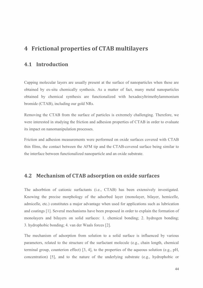
44
4 Frictional properties of CTAB multilayers
4.1 Introduction
Capping molecular layers are usually present at the surface of nanoparticles when these are
obtained by ex-situ chemically synthesis. As a matter of fact, many metal nanoparticles
obtained by chemical synthesis are functionalized with hexadecyltrimethylammonium
bromide (CTAB), including our gold NRs.
Removing the CTAB from the surface of particles is extremely challenging. Therefore, we
were interested in studying the friction and adhesion properties of CTAB in order to evaluate
its impact on nanomanipulation processes.
Friction and adhesion measurements were performed on oxide surfaces covered with CTAB
thin films, the contact between the AFM tip and the CTAB-covered surface being similar to
the interface between functionalized nanoparticle and an oxide substrate.
4.2 Mechanism of CTAB adsorption on oxide surfaces
The adsorbtion of cationic surfactants (i.e., CTAB) has been extensively investigated.
Knowing the precise morphology of the adsorbed layer (monolayer, bilayer, hemicelle,
admicelle, etc.) constitutes a major advantage when used for applications such as lubrication
and coatings [1]. Several mechanisms have been proposed in order to explain the formation of
monolayers and bilayers on solid surfaces: 1. chemical bonding; 2. hydrogen bonding;
3. hydrophobic bonding; 4. van der Waals forces [2].
The mechanism of adsorption from solution to a solid surface is influenced by various
parameters, related to the structure of the surfactant molecule (e.g., chain length, chemical
terminal group, counterion effect) [3, 4], to the properties of the aqueous solution (e.g., pH,
concentration) [5], and to the nature of the underlying substrate (e.g., hydrophobic or

45
hydrophilic, positively or negatively charged) [6]. Furthermore, the adsorption may occur as
formation of dense continuous monolayers or bilayers, or in patches or aggregates [1, 7]. In
the particular case of CTAB adsorption on silica surfaces, two adsorption mechanisms are
believed to govern the formation of the monolayer and subsequently of the bilayer [8]. The
CTAB adsorbs initially as a monolayer through a mechanism driven by electrostatic
interactions between the charged headgroups of the surfactant and the oppositely charged
surface. The headgroup anchors itself at the silica surface, while the hydrocarbon tail extends
away. Then a second monolayer will assemble on top of the first one, thanks to hydrophobic
bonding.
An important aspect of CTAB adsorption is the orientation of the molecules on the surface. It
is generally accepted that surfactants have a general tendency to adsorb in an oriented manner
with, in most cases, the long axes of the molecules being perpendicular to the surface [3, 9].
This is due to electrostatic interactions between the headgroup and the substrate, the lateral
attractions between the surfactant tails, and the repulsion of the apolar chains by the polar
surface.
4.3 AFM experiments
4.3.1 Experimental details
AFM experiments were performed with an atomic force microscope operated in lateral force
mode. For topography measurements contact mode was preferred to tapping mode, since the
former has proved more suitable for imaging soft organic films. All measurements were
carried out in vacuum, at pressures below 10-4
mbar and at room temperature. The samples
were prepared using a conventional drop-casting method of a CTAB aqueous solution on
hydrophilic silica surfaces. The silicon substrates were checked for cleanliness prior to
surfactant deposition by performing AFM imaging and approach-retract curves. After CTAB
deposition on the substrate, the samples were outgassed for several hours at pressures below
10-4
mbar to assure a complete desorption of water molecules and to avoid capillary adhesion.
The AFM probes used during the measurements had original tip radii around 10 nm and
normal and lateral probe spring constants of 0.01 and 20 N/m, respectively. The cantilever
stiffness was determined using thermal tune method.
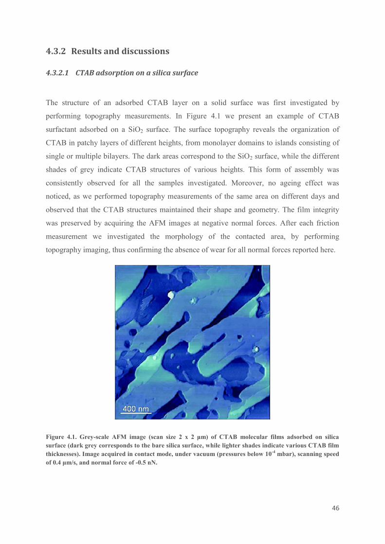
46
4.3.2 Results and discussions
4.3.2.1 CTAB adsorption on a silica surface
The structure of an adsorbed CTAB layer on a solid surface was first investigated by
performing topography measurements. In Figure 4.1 we present an example of CTAB
surfactant adsorbed on a SiO2 surface. The surface topography reveals the organization of
CTAB in patchy layers of different heights, from monolayer domains to islands consisting of
single or multiple bilayers. The dark areas correspond to the SiO2 surface, while the different
shades of grey indicate CTAB structures of various heights. This form of assembly was
consistently observed for all the samples investigated. Moreover, no ageing effect was
noticed, as we performed topography measurements of the same area on different days and
observed that the CTAB structures maintained their shape and geometry. The film integrity
was preserved by acquiring the AFM images at negative normal forces. After each friction
measurement we investigated the morphology of the contacted area, by performing
topography imaging, thus confirming the absence of wear for all normal forces reported here.
Figure 4.1. Grey-scale AFM image (scan size 2 x 2 μm) of CTAB molecular films adsorbed on silica
surface (dark grey corresponds to the bare silica surface, while lighter shades indicate various CTAB film
thicknesses). Image acquired in contact mode, under vacuum (pressures below 10-4
mbar), scanning speed
of 0.4 μm/s, and normal force of -0.5 nN.
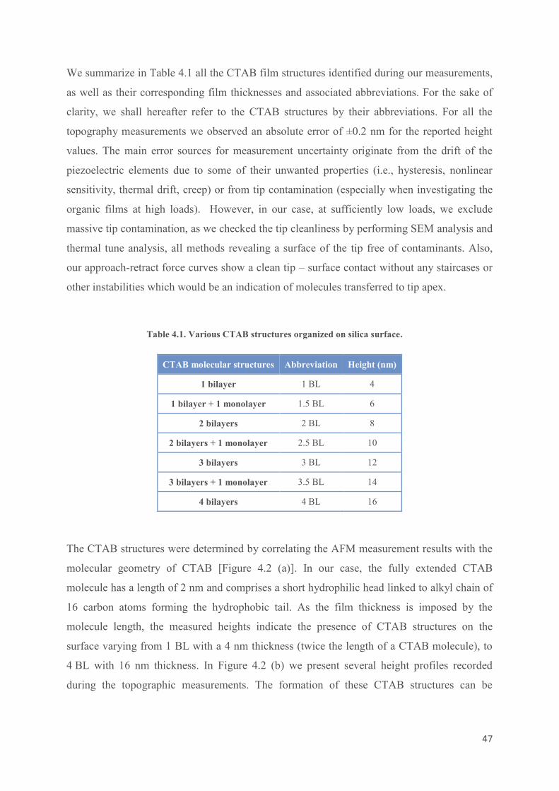
47
We summarize in Table 4.1 all the CTAB film structures identified during our measurements,
as well as their corresponding film thicknesses and associated abbreviations. For the sake of
clarity, we shall hereafter refer to the CTAB structures by their abbreviations. For all the
topography measurements we observed an absolute error of ±0.2 nm for the reported height
values. The main error sources for measurement uncertainty originate from the drift of the
piezoelectric elements due to some of their unwanted properties (i.e., hysteresis, nonlinear
sensitivity, thermal drift, creep) or from tip contamination (especially when investigating the
organic films at high loads). However, in our case, at sufficiently low loads, we exclude
massive tip contamination, as we checked the tip cleanliness by performing SEM analysis and
thermal tune analysis, all methods revealing a surface of the tip free of contaminants. Also,
our approach-retract force curves show a clean tip – surface contact without any staircases or
other instabilities which would be an indication of molecules transferred to tip apex.
Table 4.1. Various CTAB structures organized on silica surface.
CTAB molecular structures Abbreviation Height (nm)
1 bilayer 1 BL 4
1 bilayer + 1 monolayer 1.5 BL 6
2 bilayers 2 BL 8
2 bilayers + 1 monolayer 2.5 BL 10
3 bilayers 3 BL 12
3 bilayers + 1 monolayer 3.5 BL 14
4 bilayers 4 BL 16
The CTAB structures were determined by correlating the AFM measurement results with the
molecular geometry of CTAB [Figure 4.2 (a)]. In our case, the fully extended CTAB
molecule has a length of 2 nm and comprises a short hydrophilic head linked to alkyl chain of
16 carbon atoms forming the hydrophobic tail. As the film thickness is imposed by the
molecule length, the measured heights indicate the presence of CTAB structures on the
surface varying from 1 BL with a 4 nm thickness (twice the length of a CTAB molecule), to
4 BL with 16 nm thickness. In Figure 4.2 (b) we present several height profiles recorded
during the topographic measurements. The formation of these CTAB structures can be
48
explained considering the previously mentioned adsorption mechanism of a cationic
surfactant on a hydrophilic surface.
Figure 4.2. (a) CTAB molecular structure characterized by a hydrophilic head and a hydrophobic tail.
(b) Height profiles of CTAB molecular films adsorbed on silica surface correspondent to Figure 4.1.
(c) Adsorption model of CTAB on silica surface corresponding to height profiles from (b).
In the first instance a monolayer is formed due to electrostatic forces between the cationic
surfactant headgroup and the oppositely charged surface. The exposed hydrophobic surface of
the adsorbed monolayer (i.e., the hydrocarbon tails) will then attract a second layer of the
surfactant, with the hydrophilic group orientated oppositely from the surface. We consider
that the adsorption mechanism for monolayer and bilayer formation is similar for all the
structures reported here [Figure 4.2 (c)].
4.3.2.2 Friction and adhesion measurements
The frictional properties of CTAB were investigated by simultaneously acquiring topographic
and friction images. We present in Figure 4.3 (a) a topographic image which shows the
existence of three regions with different heights. The dashed blue line indicates the scan line
for both height profile [Figure 4.3 (d)] and friction profile [Figure 4.3 (e)]. The height profile
confirms the existence of three distinctive regions, the bare silica surface, 1 BL and 2.5 BL
structure. Corresponding forward and backward friction signals were recorded [Figure 4.3
(b), (c)]. Like for topography image we identify three friction regimes. The highest friction
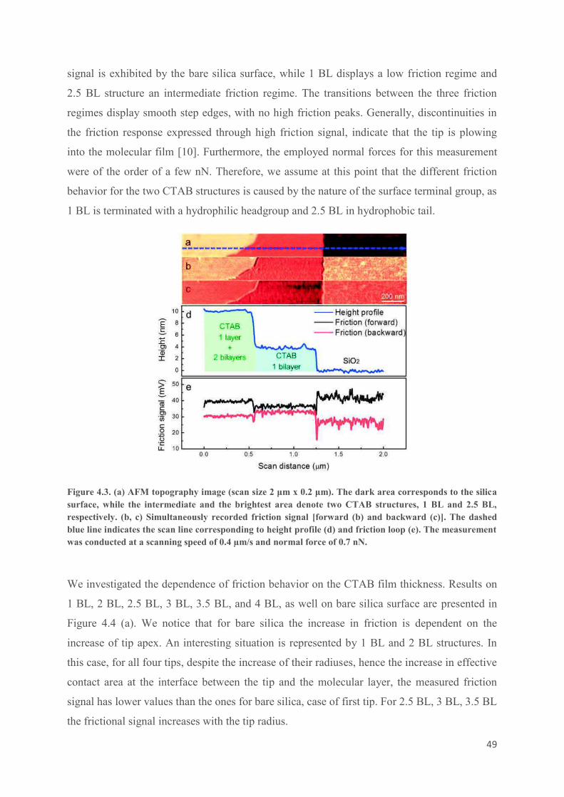
49
signal is exhibited by the bare silica surface, while 1 BL displays a low friction regime and
2.5 BL structure an intermediate friction regime. The transitions between the three friction
regimes display smooth step edges, with no high friction peaks. Generally, discontinuities in
the friction response expressed through high friction signal, indicate that the tip is plowing
into the molecular film [10]. Furthermore, the employed normal forces for this measurement
were of the order of a few nN. Therefore, we assume at this point that the different friction
behavior for the two CTAB structures is caused by the nature of the surface terminal group, as
1 BL is terminated with a hydrophilic headgroup and 2.5 BL in hydrophobic tail.
Figure 4.3. (a) AFM topography image (scan size 2 μm x 0.2 μm). The dark area corresponds to the silica
surface, while the intermediate and the brightest area denote two CTAB structures, 1 BL and 2.5 BL,
respectively. (b, c) Simultaneously recorded friction signal [forward (b) and backward (c)]. The dashed
blue line indicates the scan line corresponding to height profile (d) and friction loop (e). The measurement
was conducted at a scanning speed of 0.4 µm/s and normal force of 0.7 nN.
We investigated the dependence of friction behavior on the CTAB film thickness. Results on
1 BL, 2 BL, 2.5 BL, 3 BL, 3.5 BL, and 4 BL, as well on bare silica surface are presented in
Figure 4.4 (a). We notice that for bare silica the increase in friction is dependent on the
increase of tip apex. An interesting situation is represented by 1 BL and 2 BL structures. In
this case, for all four tips, despite the increase of their radiuses, hence the increase in effective
contact area at the interface between the tip and the molecular layer, the measured friction
signal has lower values than the ones for bare silica, case of first tip. For 2.5 BL, 3 BL, 3.5 BL
the frictional signal increases with the tip radius.
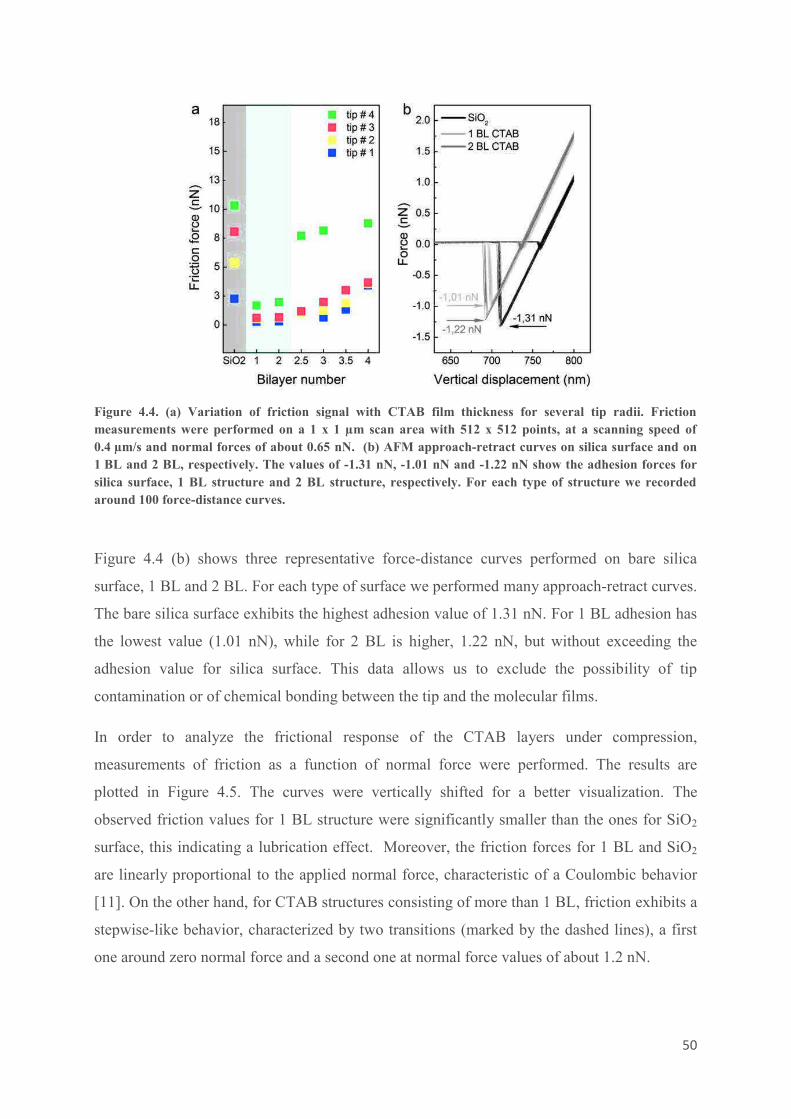
50
Figure 4.4. (a) Variation of friction signal with CTAB film thickness for several tip radii. Friction
measurements were performed on a 1 x 1 µm scan area with 512 x 512 points, at a scanning speed of
0.4 µm/s and normal forces of about 0.65 nN. (b) AFM approach-retract curves on silica surface and on
1 BL and 2 BL, respectively. The values of -1.31 nN, -1.01 nN and -1.22 nN show the adhesion forces for
silica surface, 1 BL structure and 2 BL structure, respectively. For each type of structure we recorded
around 100 force-distance curves.
Figure 4.4 (b) shows three representative force-distance curves performed on bare silica
surface, 1 BL and 2 BL. For each type of surface we performed many approach-retract curves.
The bare silica surface exhibits the highest adhesion value of 1.31 nN. For 1 BL adhesion has
the lowest value (1.01 nN), while for 2 BL is higher, 1.22 nN, but without exceeding the
adhesion value for silica surface. This data allows us to exclude the possibility of tip
contamination or of chemical bonding between the tip and the molecular films.
In order to analyze the frictional response of the CTAB layers under compression,
measurements of friction as a function of normal force were performed. The results are
plotted in Figure 4.5. The curves were vertically shifted for a better visualization. The
observed friction values for 1 BL structure were significantly smaller than the ones for SiO2
surface, this indicating a lubrication effect. Moreover, the friction forces for 1 BL and SiO2
are linearly proportional to the applied normal force, characteristic of a Coulombic behavior
[11]. On the other hand, for CTAB structures consisting of more than 1 BL, friction exhibits a
stepwise-like behavior, characterized by two transitions (marked by the dashed lines), a first
one around zero normal force and a second one at normal force values of about 1.2 nN.
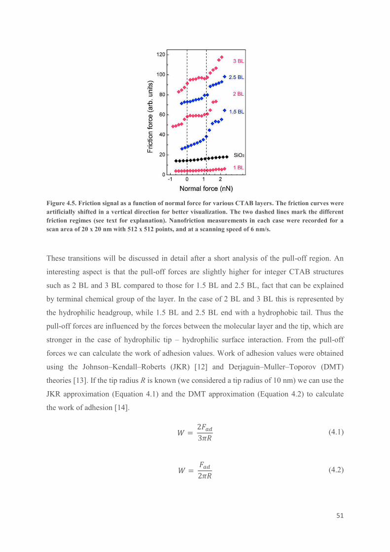
51
Figure 4.5. Friction signal as a function of normal force for various CTAB layers. The friction curves were
artificially shifted in a vertical direction for better visualization. The two dashed lines mark the different
friction regimes (see text for explanation). Nanofriction measurements in each case were recorded for a
scan area of 20 x 20 nm with 512 x 512 points, and at a scanning speed of 6 nm/s.
These transitions will be discussed in detail after a short analysis of the pull-off region. An
interesting aspect is that the pull-off forces are slightly higher for integer CTAB structures
such as 2 BL and 3 BL compared to those for 1.5 BL and 2.5 BL, fact that can be explained
by terminal chemical group of the layer. In the case of 2 BL and 3 BL this is represented by
the hydrophilic headgroup, while 1.5 BL and 2.5 BL end with a hydrophobic tail. Thus the
pull-off forces are influenced by the forces between the molecular layer and the tip, which are
stronger in the case of hydrophilic tip – hydrophilic surface interaction. From the pull-off
forces we can calculate the work of adhesion values. Work of adhesion values were obtained
using the Johnson–Kendall–Roberts (JKR) [12] and Derjaguin–Muller–Toporov (DMT)
theories [13]. If the tip radius R is known (we considered a tip radius of 10 nm) we can use the
JKR approximation (Equation 4.1) and the DMT approximation (Equation 4.2) to calculate
the work of adhesion [14].
v =1q5@6VwM (4.1)
v =1 5@6qwM (4.2)
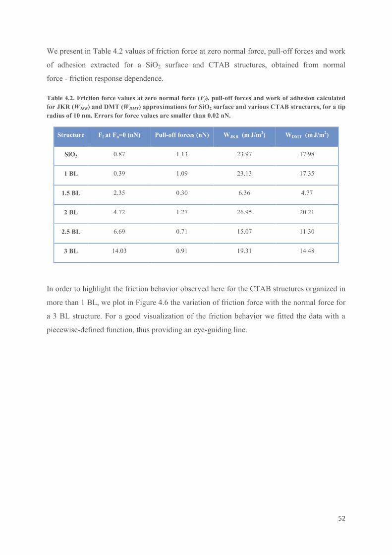
52
We present in Table 4.2 values of friction force at zero normal force, pull-off forces and work
of adhesion extracted for a SiO2 surface and CTAB structures, obtained from normal
force - friction response dependence.
Table 4.2. Friction force values at zero normal force (Ff), pull-off forces and work of adhesion calculated
for JKR (WJKR) and DMT (WDMT) approximations for SiO2 surface and various CTAB structures, for a tip
radius of 10 nm. Errors for force values are smaller than 0.02 nN.
Structure Ff at Fn=0 (nN) Pull-off forces (nN) WJKR (m J/m2) WDMT (m J/m
2)
SiO2 0.87 1.13 23.97 17.98
1 BL 0.39 1.09 23.13 17.35
1.5 BL 2.35 0.30 6.36 4.77
2 BL 4.72 1.27 26.95 20.21
2.5 BL 6.69 0.71 15.07 11.30
3 BL 14.03 0.91 19.31 14.48
In order to highlight the friction behavior observed here for the CTAB structures organized in
more than 1 BL, we plot in Figure 4.6 the variation of friction force with the normal force for
a 3 BL structure. For a good visualization of the friction behavior we fitted the data with a
piecewise-defined function, thus providing an eye-guiding line.
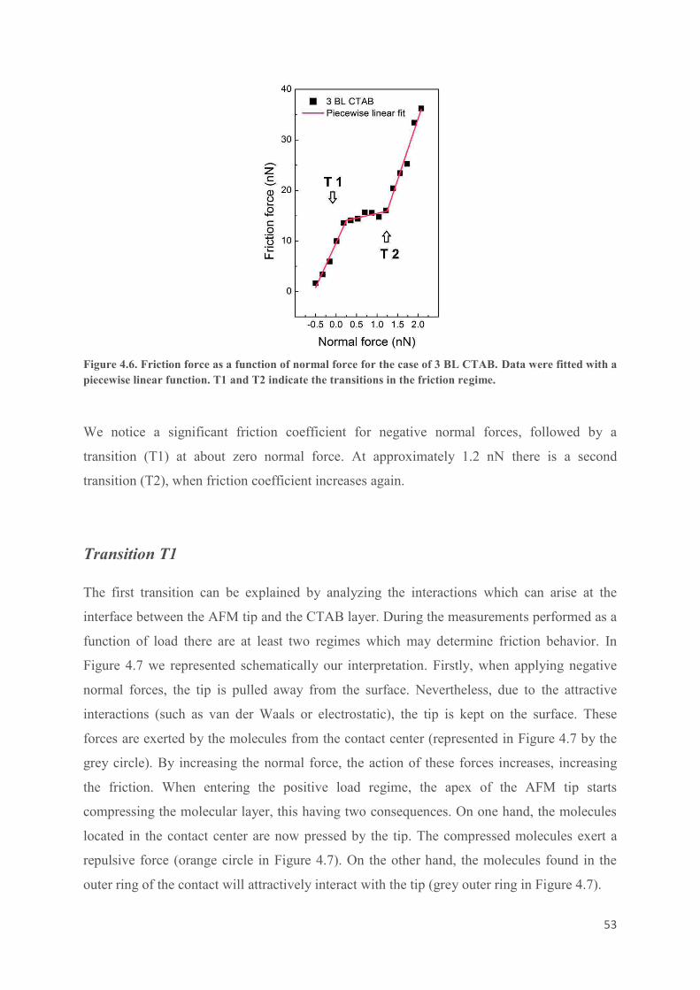
53
Figure 4.6. Friction force as a function of normal force for the case of 3 BL CTAB. Data were fitted with a
piecewise linear function. T1 and T2 indicate the transitions in the friction regime.
We notice a significant friction coefficient for negative normal forces, followed by a
transition (T1) at about zero normal force. At approximately 1.2 nN there is a second
transition (T2), when friction coefficient increases again.
Transition T1
The first transition can be explained by analyzing the interactions which can arise at the
interface between the AFM tip and the CTAB layer. During the measurements performed as a
function of load there are at least two regimes which may determine friction behavior. In
Figure 4.7 we represented schematically our interpretation. Firstly, when applying negative
normal forces, the tip is pulled away from the surface. Nevertheless, due to the attractive
interactions (such as van der Waals or electrostatic), the tip is kept on the surface. These
forces are exerted by the molecules from the contact center (represented in Figure 4.7 by the
grey circle). By increasing the normal force, the action of these forces increases, increasing
the friction. When entering the positive load regime, the apex of the AFM tip starts
compressing the molecular layer, this having two consequences. On one hand, the molecules
located in the contact center are now pressed by the tip. The compressed molecules exert a
repulsive force (orange circle in Figure 4.7). On the other hand, the molecules found in the
outer ring of the contact will attractively interact with the tip (grey outer ring in Figure 4.7).

54
Figure 4.7. Illustration depicting an AFM tip – CTAB molecules interaction (adapted from [15]).
The competition between the attractive and repulsive “zones” establishes an equilibrium
position leading to a significant decrease of friction coefficient.
A similar model which considers the contribution of van der Waals forces to effective
adhesion was described by Ptak et al. for an AFM tip interacting with a hydrophobic
monolayer [15]. Although there are discussed adhesion forces, we consider that the transition
T1 can be explained by their model, which has been at the origin of our interpretations.
Transition T2
The second transition in the friction response takes place in repulsive regime, at a normal
force value of about 1.2 nN (Figure 4.6). To gain insight into the origin of this transition we
performed measurements of height and friction as a function of normal force. In the case
presented here, height and friction images were recorded simultaneously for a scanned area of
1.6 x 1.6 μm, where half of the surface was bare silica and the other half was covered by a
2.5 BL CTAB. The results (see for instance Figure 4.8) reveal height modifications induced
by increasing load. It is worth mentioning that for this measurement we used a new sharp
AFM probe, this explaining the low pull-off force values found for this measurement. Four
representative height profiles are presented in Figure 4.8. Each curve was recorded at a
different normal force of 0.37 nN, 1.04 nN, 1.56 nN, and 2.07 nN, respectively. For an initial
normal force of 0.37 nN, the 2.5 BL shows a height of 10.2 nm. As normal force increases,
for example to 1.04 nN, the measured height has a value of 9.6 nm. A second increase to
1.56 nN gives a layer height of 9.0 nm. Nonetheless, the molecular layer undergoes height
loss only up to a certain normal force value. For example, in Figure 4.8, the dark green curve
was recorded at a normal force of 2.07 nN and shows a height of 9.6 nm.
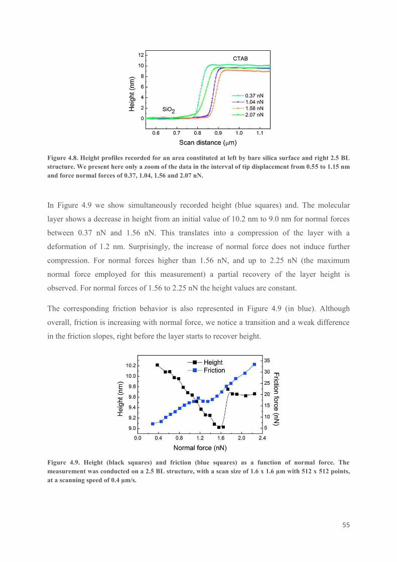
55
Figure 4.8. Height profiles recorded for an area constituted at left by bare silica surface and right 2.5 BL
structure. We present here only a zoom of the data in the interval of tip displacement from 0.55 to 1.15 nm
and force normal forces of 0.37, 1.04, 1.56 and 2.07 nN.
In Figure 4.9 we show simultaneously recorded height (blue squares) and. The molecular
layer shows a decrease in height from an initial value of 10.2 nm to 9.0 nm for normal forces
between 0.37 nN and 1.56 nN. This translates into a compression of the layer with a
deformation of 1.2 nm. Surprisingly, the increase of normal force does not induce further
compression. For normal forces higher than 1.56 nN, and up to 2.25 nN (the maximum
normal force employed for this measurement) a partial recovery of the layer height is
observed. For normal forces of 1.56 to 2.25 nN the height values are constant.
The corresponding friction behavior is also represented in Figure 4.9 (in blue). Although
overall, friction is increasing with normal force, we notice a transition and a weak difference
in the friction slopes, right before the layer starts to recover height.
Figure 4.9. Height (black squares) and friction (blue squares) as a function of normal force. The
measurement was conducted on a 2.5 BL structure, with a scan size of 1.6 x 1.6 µm with 512 x 512 points,
at a scanning speed of 0.4 µm/s.

56
To explain these findings we chose from data plotted in Figure 4.9 four values of normal
forces to schematically represent the behavior of the molecular layer under compression
(Figure 4.10). We interpret our results with a model based on molecular tilting and load
induced order – disorder transition, when the AFM tip produces conformational and structural
changes most likely in the top monolayer of the 2.5 BL structure. In the case of a normal force
of 0.37 nN the layer bears the load applied by the AFM tip and no changes are observed in the
molecular configuration, the molecules keeping their vertical configuration. An increase of
normal force determines a tilt of the molecules, associated with height decrease [(b) in Figure
4.10]. This occurs until the pressure is high enough to induce a molecular reorganization
[(d) in Figure 4.10)].
Figure 4.10. Schematics representing changes of the molecular structure under the increase of normal
force (Fn). (a) For Fn=0.37 nN the layer keeps its stability and the molecules retain their perpendicular
orientation towards the surface. (b, c) At Fn=1.04 nN and Fn=1.56 nN the passage of the AFM tip causes a
molecular tilting. (d) For Fn=2.07 nN the pressure exerted by the tip is high enough to induce an order –
disorder transition. Similar effects are expected on all CTAB film thicknesses. For 1 BL, however, the
transition seems to occur at higher normal force values.
A similar behavior has been observed in the case of self-assembled monolayers of n-
alkanethiols [16]. The first three situations (a – c) are characteristic of an ordered state of the
molecular layer, while the last one suggests a disordered state (d) accompanied by a height
regain.
The structural arrangement of the chain-like pressed molecules in the layer was shown to have
a considerable impact on the frictional properties of an organic monolayer, with increasing
load. The interpretations and analyses are done by considering two different mechanisms, the
formation of gauche defects in the hydrocarbon chains and cooperative molecular tilting
models [17 25]. The process of gauche distortions comprises an initial phase where terminal
gauche rotations occur and a second phase represented by internal gauche deformation. The
creation of gauche defects in the hydrocarbon chains leads to additional modes of energy
dissipation, hence, an increase in the frictional response. To confirm the presence of gauche
defects in our case, the first step was to calculate the energy transferred from the tip to the
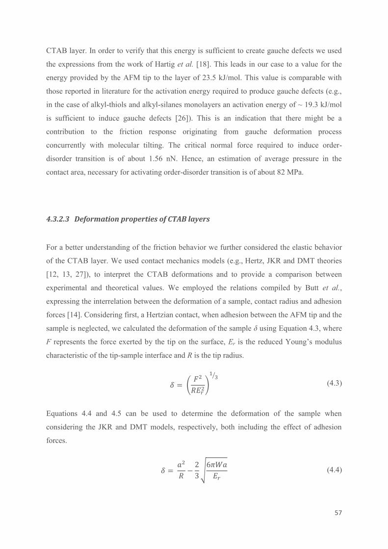
57
CTAB layer. In order to verify that this energy is sufficient to create gauche defects we used
the expressions from the work of Hartig et al. [18]. This leads in our case to a value for the
energy provided by the AFM tip to the layer of 23.5 kJ/mol. This value is comparable with
those reported in literature for the activation energy required to produce gauche defects (e.g.,
in the case of alkyl-thiols and alkyl-silanes monolayers an activation energy of ~ 19.3 kJ/mol
is sufficient to induce gauche defects [26]). This is an indication that there might be a
contribution to the friction response originating from gauche deformation process
concurrently with molecular tilting. The critical normal force required to induce order-
disorder transition is of about 1.56 nN. Hence, an estimation of average pressure in the
contact area, necessary for activating order-disorder transition is of about 82 MPa.
4.3.2.3 Deformation properties of CTAB layers
For a better understanding of the friction behavior we further considered the elastic behavior
of the CTAB layer. We used contact mechanics models (e.g., Hertz, JKR and DMT theories
[12, 13, 27]), to interpret the CTAB deformations and to provide a comparison between
experimental and theoretical values. We employed the relations compiled by Butt et al.,
expressing the interrelation between the deformation of a sample, contact radius and adhesion
forces [14]. Considering first, a Hertzian contact, when adhesion between the AFM tip and the
sample is neglected, we calculated the deformation of the sample δ using Equation 4.3, where
F represents the force exerted by the tip on the surface, Er is the reduced Young’s modulus
characteristic of the tip-sample interface and R is the tip radius.
x = 1y 5.MF7.zt p{
(4.3)
Equations 4.4 and 4.5 can be used to determine the deformation of the sample when
considering the JKR and DMT models, respectively, both including the effect of adhesion
forces.
x = 1|.M R qV}Nwv|F7 (4.4)
58
x = 1 (5 0 qwMv). p{sMF7.~ (4.5)
The work of adhesion W, was determined using the Equations 4.1 for JKR and Equation 4.2
for DMT model. Contact radius a, was obtained using Equation 4.6 (JKR) and Equation 4.7
(DMT).
| = 1 }MF7 X5 0 VwMv 0sNwMv5 0 (VwMv).[~ (4.6)
| = 1 }MF7 (5 0 qwMv)~ (4.7)
The determination of the reduced Young’s modulus was done using Equation 4.8, where Es
and Et are the Young’s moduli for the sample and the tip, respectively and νs and νt represent
Poisson’s ratios for the sample and the tip, respectively.
�F7 =1� R n�.
F� 0 � R nB.FB (4.8)
Nevertheless, determining the reduced Young’s modulus was not at all a trivial task. If for a
silicon nitride tip the elastic modulus and Poisson’s ratio are well-documented, with reported
values in the interval of 130 ÷ 290 GPa and 0.2 ÷ 0.3, respectively [28 30], coherent values
for elastic modulus and Poisson’s ratio of CTAB are hardly found in literature [22, 31]. As a
starting point for our subsequent calculations we chose as a reference range for the elastic
modulus of CTAB the one reported by Rabinovich et al. [31], of few MPa, since there are
several similitudes between their work and ours regarding the CTAB layer (e.g., film
thickness, chain length, etc.). As for the Poisson’s ratio we used a value of 0.5. For the silicon
nitride tip, we used an elastic modulus value of 148 GPa determined with Equation 4., where
k is the cantilever’s spring constant (determined by thermal tune method), l, w, and f0 are
cantilever’s length, width and fundamental resonance frequency, respectively, while ρ and E
represent the mass density of the cantilever’s material and the Young’s modulus of elasticity,
respectively. For the Poisson’s ratio we assumed a value of 0.25.
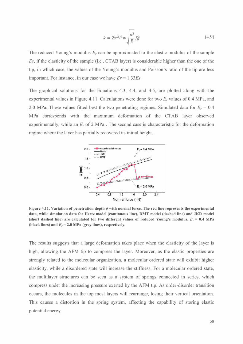
59
a = qwplp�}�pF rZp (4.9)
The reduced Young’s modulus Er can be approximated to the elastic modulus of the sample
Es, if the elasticity of the sample (i.e., CTAB layer) is considerable higher than the one of the
tip, in which case, the values of the Young’s modulus and Poisson’s ratio of the tip are less
important. For instance, in our case we have Er = 1.33Es.
The graphical solutions for the Equations 4.3, 4.4, and 4.5, are plotted along with the
experimental values in Figure 4.11. Calculations were done for two Er values of 0.4 MPa, and
2.0 MPa. These values fitted best the two penetrating regimes. Simulated data for Er = 0.4
MPa corresponds with the maximum deformation of the CTAB layer observed
experimentally, while an Er of 2 MPa . The second case is characteristic for the deformation
regime where the layer has partially recovered its initial height.
Figure 4.11. Variation of penetration depth δ with normal force. The red line represents the experimental
data, while simulation data for Hertz model (continuous line), DMT model (dashed line) and JKR model
(short dashed line) are calculated for two different values of reduced Young’s modulus, Er = 0.4 MPa
(black lines) and Er = 2.0 MPa (grey lines), respectively.
The results suggests that a large deformation takes place when the elasticity of the layer is
high, allowing the AFM tip to compress the layer. Moreover, as the elastic properties are
strongly related to the molecular organization, a molecular ordered state will exhibit higher
elasticity, while a disordered state will increase the stiffness. For a molecular ordered state,
the multilayer structures can be seen as a system of springs connected in series, which
compress under the increasing pressure exerted by the AFM tip. As order-disorder transition
occurs, the molecules in the top most layers will rearrange, losing their vertical orientation.
This causes a distortion in the spring system, affecting the capability of storing elastic
potential energy.

60
4.4 Elastic recovery and plowing friction
The term of plowing employed in the context of an AFM friction force measurement defines
the lateral movement of a tip through a compliant layer. In the case of an elastic layer, the
pressed molecules will recover after the passage of the AFM tip, defining a rear contact angle.
This will have a direct effect on the friction coefficient and on the total frictional response.
Plowing friction models found in literature describe tribological contacts from macroscale to
nanoscale [21, 32 38]. In our case, we employed the analytical model developed by
Lafaye et al. [39]. The model describes the plowing coefficient in the case of an elastic
recovery at the back of the sliding tip, by considering the vertical and the horizontal
projections of the contact area between the tip and the sample. Assuming a spherical tip and a
penetration depth smaller than the tip radius, the plowing coefficient µp is given by the ratio
between the vertical projection AVep and the horizontal projection AHep:
�` =1 K���KL�� (4.10)
The vertical and horizontal projections of the contact area incorporate the elastic recovery of
the molecules after the passage of the tip and can be determined solving Equations 4.11 and
4.12, respectively, where a represents the contact radius, and ω is the angle formed between
the rear of the tip and the recovered layer (Figure 4.12). The vertical projection takes into
account the cross section of the contact area which is defined by Equation 4.13, where R is the
tip radius.
K��� =1�.��m$t �|���I� � R |���Is�. R |.���.I (4.11)
KL�� =1|.q (w 0 I 0 ��mqI) (4.12)
�. =1M. R |.��m.I (4.13)
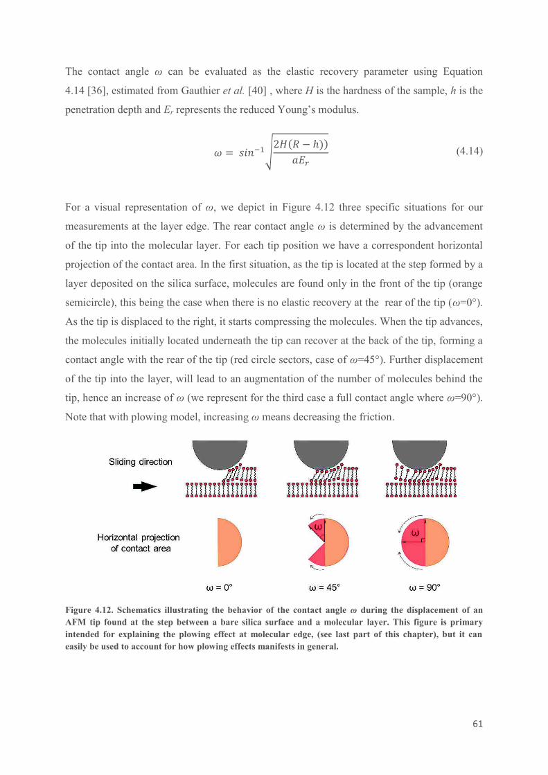
61
The contact angle ω can be evaluated as the elastic recovery parameter using Equation
4.14 [36], estimated from Gauthier et al. [40] , where H is the hardness of the sample, h is the
penetration depth and Er represents the reduced Young’s modulus.
I =1��m$t}q�(M R �))|F7 (4.14)
For a visual representation of ω, we depict in Figure 4.12 three specific situations for our
measurements at the layer edge. The rear contact angle ω is determined by the advancement
of the tip into the molecular layer. For each tip position we have a correspondent horizontal
projection of the contact area. In the first situation, as the tip is located at the step formed by a
layer deposited on the silica surface, molecules are found only in the front of the tip (orange
semicircle), this being the case when there is no elastic recovery at the rear of the tip (ω=0°).
As the tip is displaced to the right, it starts compressing the molecules. When the tip advances,
the molecules initially located underneath the tip can recover at the back of the tip, forming a
contact angle with the rear of the tip (red circle sectors, case of ω=45°). Further displacement
of the tip into the layer, will lead to an augmentation of the number of molecules behind the
tip, hence an increase of ω (we represent for the third case a full contact angle where ω=90°).
Note that with plowing model, increasing ω means decreasing the friction.
Figure 4.12. Schematics illustrating the behavior of the contact angle ω during the displacement of an
AFM tip found at the step between a bare silica surface and a molecular layer. This figure is primary
intended for explaining the plowing effect at molecular edge, (see last part of this chapter), but it can
easily be used to account for how plowing effects manifests in general.
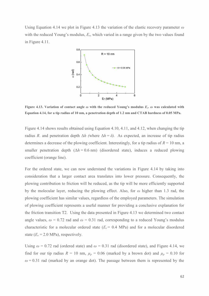
62
Using Equation 4.14 we plot in Figure 4.13 the variation of the elastic recovery parameter ω
with the reduced Young’s modulus, Er, which varied in a range given by the two values found
in Figure 4.11.
Figure 4.13. Variation of contact angle ω with the reduced Young’s modulus Er. ω was calculated with
Equation 4.14, for a tip radius of 10 nm, a penetration depth of 1.2 nm and CTAB hardness of 0.05 MPa.
Figure 4.14 shows results obtained using Equation 4.10, 4.11, and 4.12, when changing the tip
radius R. and penetration depth Δh (where Δh = δ). As expected, an increase of tip radius
determines a decrease of the plowing coefficient. Interestingly, for a tip radius of R = 10 nm, a
smaller penetration depth (Δh = 0.6 nm) (disordered state), induces a reduced plowing
coefficient (orange line).
For the ordered state, we can now understand the variations in Figure 4.14 by taking into
consideration that a larger contact area translates into lower pressure. Consequently, the
plowing contribution to friction will be reduced, as the tip will be more efficiently supported
by the molecular layer, reducing the plowing effect. Also, for ω higher than 1.3 rad, the
plowing coefficient has similar values, regardless of the employed parameters. The simulation
of plowing coefficient represents a useful manner for providing a conclusive explanation for
the friction transition T2. Using the data presented in Figure 4.13 we determined two contact
angle values, ω = 0.72 rad and ω = 0.31 rad, corresponding to a reduced Young’s modulus
characteristic for a molecular ordered state (Er = 0.4 MPa) and for a molecular disordered
state (Er = 2.0 MPa), respectively.
Using ω = 0.72 rad (ordered state) and ω = 0.31 rad (disordered state), and Figure 4.14, we
find for our tip radius R = 10 nm, µp = 0.06 (marked by a brown dot) and µp = 0.10 for
ω = 0.31 rad (marked by an orange dot). The passage between them is represented by the

63
green arrow, and it actually depicts the transition T2 observed for the frictional behavior of
multilayered CTAB structures at the critical normal force of 1.2 nN [see Figure 4.5].
Figure 4.14. Variation of plowing coefficient µp with contact angle ω. Simulations were based on
experimental values (wine line for tip radius R = 10 nm and penetration depth δ = 1.2 nm, and orange line
for R = 10 nm and δ = 1.2 nm). Grey lines show the evolution of µp as a function of ω. The red and orange
dots mark two particular cases for µp, representative for two distinct values of the reduced Young’s
modulus (see text for explanation). The green arrow designates the transition T2 observed in the frictional
response of CTAB structures greater than 1 BL.
In conclusion, in the disordered state the friction coefficient is increased by a higher plowing
coefficient, i.e., less molecular recovery at the back of the tip.
Checking plowing effects: Friction at a layer edge
The findings described above were confirmed by conducting friction experiments across a
molecular layer edge. When the tip scans perpendicularly to a step edge, the elastic recovery
effects are delayed because there are no available molecules behind the tip, although the front
side already plows into the layer. This effect keeps ω close to zero for a few nanometers after
the tip starts to plow into the layer. According to the plowing model, the friction must reach
large values and then drop again as molecules become available at the rear of the tip. This is
precisely what is depicted in Figure 4.12 and also found experimentally (Figure 4.15). In
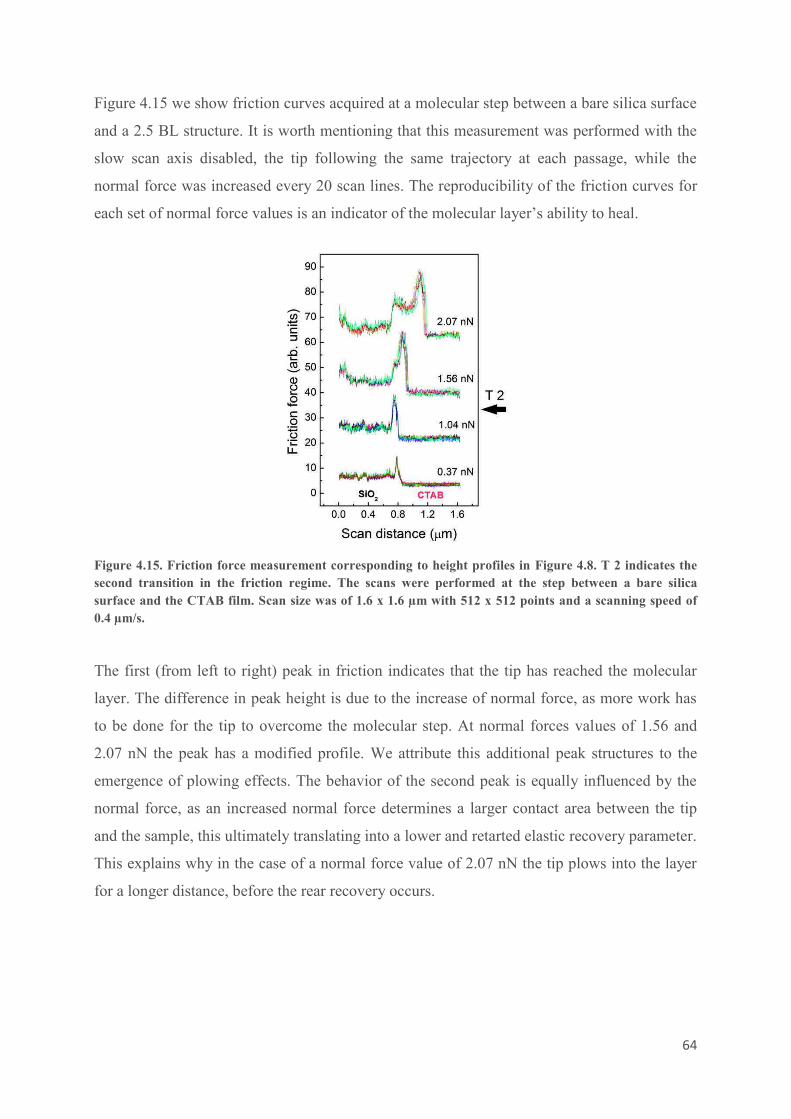
64
Figure 4.15 we show friction curves acquired at a molecular step between a bare silica surface
and a 2.5 BL structure. It is worth mentioning that this measurement was performed with the
slow scan axis disabled, the tip following the same trajectory at each passage, while the
normal force was increased every 20 scan lines. The reproducibility of the friction curves for
each set of normal force values is an indicator of the molecular layer’s ability to heal.
Figure 4.15. Friction force measurement corresponding to height profiles in Figure 4.8. T 2 indicates the
second transition in the friction regime. The scans were performed at the step between a bare silica
surface and the CTAB film. Scan size was of 1.6 x 1.6 µm with 512 x 512 points and a scanning speed of
0.4 µm/s.
The first (from left to right) peak in friction indicates that the tip has reached the molecular
layer. The difference in peak height is due to the increase of normal force, as more work has
to be done for the tip to overcome the molecular step. At normal forces values of 1.56 and
2.07 nN the peak has a modified profile. We attribute this additional peak structures to the
emergence of plowing effects. The behavior of the second peak is equally influenced by the
normal force, as an increased normal force determines a larger contact area between the tip
and the sample, this ultimately translating into a lower and retarted elastic recovery parameter.
This explains why in the case of a normal force value of 2.07 nN the tip plows into the layer
for a longer distance, before the rear recovery occurs.

65
4.5 Conclusions
We investigated the frictional and adhesion properties of CTAB adsorbed on silica surfaces,
in order to determine its role on Au NRs manipulation. Surface topography revealed the
organization of CTAB in patchy layers of different heights, from monolayer domains to single
or multiple bilayers. We observed a non-monotonic friction vs. load behavior, which we
explained using a plowing friction model. Our study also showed that CTAB, when adsorbed
as one bilayer acts as an efficient lubricant at the interface between Au NRs and the silica
surface. The unveiled lubricant properties of CTAB were consequently exploited for
optimizing the AFM nanoparticle manipulation process. The friction studies on CTAB
multilayers also allow us to understand that nanomanipulation on thick CTAB layers is
probably too complex for an easy manipulation for NRs. A single BL of CTAB at the surface
of NRs then appears as an optimal solution, presenting a double advantage: lubrication and
cleanliness of the surface. The findings discussed in this chapter also motivate us to develop
samples preparation protocols which guarantee the removal of CTAB excess after the NRs
deposition, and before nanomanipulation experiments.
66
References
[1] B. G. Sharma, S. Basu and M. M. Sharma, "Characterization of adsorbed ionic
surfactants on a mica substrate," Langmuir, vol. 12, pp. 6506-6512, 1996.
[2] S. K. Parida, S. Dash, S. Patel and B. K. Mishra, "Adsorption of organic molecules on
silica surface," Advances in Colloid and Interface Science , vol. 121, pp. 77-110, 2006.
[3] J. Zajac, J. L. Trompette and S. Partyka, "Adsorption of cationic surfactants on a
hydrophilic silca surface at low coverages: effects of the surfactant alkyl chain and
exchangeable sodium cations at the silica surface," Langmuir, vol. 12, pp. 1357-1367,
1996.
[4] S. B. Velegol, B. D. Fleming, S. Biggs, E. J. Wanless and R. D. Tilton, "Counterion
effects on hexadecyltrimethylammonium surfactant adsorption and self-assembly on
silica," Langmuir, vol. 16, pp. 2548-2556, 2000.
[5] B. H. Bijsterbosch, "Characterization of silica surfaces by adsorption from solution.
Investigations into the mechanism of adsorbtion of cationic surfactants," Journal of
Colloid and Interface Science, vol. 47, no. 1, 1974.
[6] T. Wangchareansak, V. S. Craig and S. M. Notley, "Adsorption isotherms and structure
of cationic surfactants adsorbed on mineral oxide surfaces prepared by atomic layer
deposition," Langmuir, vol. 29, pp. 14748-14755, 2013.
[7] R. Atkin, V. S. Craig and S. Biggs, "Adsorption kinetics and structural arrangements of
cationic surfactants on silica surfaces," Langmuir, vol. 16, pp. 9374-9380, 2000.
[8] J. C. Schulz and G. G. Warr, "Adsorbed layer structure of cationic and anionic
surfactants on mineral oxide surfaces," Langmuir, vol. 18, pp. 3191-3197, 2002.
[9] S. Paria and K. C. Khilar, "A review on experimental studies of surfactant adsorption at
the hydrophilic solid-water interface," Advances in Colloid and Interface Science, vol.
110, no. 3, pp. 75-95, 2004.
[10] K. C. Wagner, Y. Wang, S. L. Regen and D. V. Vezenov, "Yield strength of glued
Langmuir–Blodgett films determined by friction force microscopy," Physical Chemistry
Chemical Physics, vol. 15, pp. 14037-14046, 2013.
[11] E. Gnecco and E. Meyer, Nanoscale friction of self-assembled monolayers, Berlin:
Springer Berlin Heidelberg, 2007, pp. 619-645.
[12] K. L. Johnson, K. Kendall and A. D. Roberts, "Surface energy and the contact of elastic
67
solids," Proceedings of the Royal Society of London A, vol. 324, pp. 301-313, 1971.
[13] B. V. Derjaguin, V. M. Muller and Y. P. Toporov, "Effect of contact deformations on the
adhesion of particles," Journal of Colloid and Interface Science, vol. 53, no. 2, pp. 314-
326, 1975.
[14] H.-J. Butt, B. Cappella and M. Kappl, "Force measurements with the atomic force
microscope: Technique, interpretation and applications," Surface Science Reports, vol.
59, pp. 1-152, 2005.
[15] A. Ptak, H. Gojzewski, M. Kappl and H.-J. Butt, "Quantitative analysis of the interaction
between an atomic force microscopy tip and a hydrophobic monolayer," Journal of
Physical Chemistry C, vol. 114, pp. 21572-21578, 2010.
[16] S. A. Joyce, R. C. Thomas, J. E. Houston, T. A. Michalske and R. M. Crooks,
"Mechanical relaxation of organic monolayer films measured by force microscopy,"
Physical Review Letters, vol. 68, no. 18, pp. 2790-2793, 1992.
[17] X. Xiao, J. Hu, D. H. Charych and M. Salmeron, "Chain length dependence of the
frictional properties of alkylsilane molecules self-assembled on mica studied by atomic
force microscopy," Langmuir, vol. 12, pp. 235-237, 1996.
[18] M. Hartig, L. F. Chi, X. D. Liu and H. Fuchs, "Dependence of the measured monolayer
height on applied forces in scanning force microscopy," Thin Solid Films, vol. 327–329,
p. 262–267, 1998.
[19] E. Barrena, S. Kopta, D. F. Ogletree, D. H. Charych and M. Salmeron, "Relationship
between friction and molecular structure: alkylsilane lubricant films under pressure,"
Physical Review Letters, vol. 82, no. 14, pp. 2880-2883, 1999.
[20] M. Chandross, G. S. Grest and M. J. Stevens, "Friction between alkylsilane monolayers:
molecular simulation of ordered monolayers," Langmuir, vol. 18, no. 22, pp. 8392-8399,
2002.
[21] E. E. Flater, W. R. Ashurst and R. W. Carpick, "Nanotribology of
octadecyltrichlorosilane monolayers and silicon: self-mated versus unmated interfaces
and local packing density effects," Langmuir, vol. 23, no. 18, pp. 9242-9252, 2007.
[22] G. Oncins, C. Vericat and F. Sanz, "Mechanical properties of alkanethiol monolayers
studied by force spectroscopy," Journal of Chemical Physics, vol. 128, p. 044701, 2008.
[23] I. Szlufarska, M. Chandross and R. W. Carpick, "Recent advances in single-asperity
nanotribology," Journal of Physics D: Applied Physics, vol. 41, p. 123001, 2008.
68
[24] L. Lu and Y. Cai, "Molecular tilting and its impact on frictional properties of n-alkane
self-assembled monolayers," Langmuir, vol. 27, p. 5953–5960, 2011.
[25] N. N. Gosvami, P. Egberts and R. Bennewitz, "Molecular order and disorder in the
frictional response of alkanethiol self-assembled monolayers," Journal of Physical
Chemistry A, vol. 115, p. 6942–6947, 2011.
[26] M. Salmeron, S. Kopta, E. Barrena and C. Ocal, "Atomic scale origin of adhesion and
friction," in Fundamentals of tribology and bridging the gap between the macro- and
micro/nanoscales, B. Bhushan, Ed., Dordrecht , Springer Netherlands, 2001, pp. 41-52.
[27] H. Hertz, "On the contact of elastic solids," Journal für die reine und angewandte
Mathematik, vol. 92, p. 156, 1881.
[28] J. E. Sader, I. Larson, P. Mulvaney and L. R. White, "Method for the calibration of
atomic force microscope cantilevers," Review of Scientific Instruments, vol. 66, no. 7, pp.
3789-3798, 1995.
[29] Z. Wei, C. Wang and C. Bai, "Investigation of nanoscale frictional contact by friction
force microscopy," Langmuir, vol. 17, pp. 3945-3951, 2001.
[30] A. Khan, J. Philip and P. Hess, "Young’s modulus of silicon nitride used in scanning
force microscope cantilevers," Journal of Applied Physics, vol. 95, no. 4, pp. 1667-1672,
2004.
[31] Y. I. Rabinovich, I. U. Vakarelski, S. C. Brown, P. K. Singh and B. M. Moudgil,
"Mechanical and thermodynamic properties of surfactant aggregates at the solid-liquid
interface," Journal of Colloid and Interface Science, vol. 270, pp. 29-36, 2004.
[32] F. P. Bowden and D. Tabor, The friction and lubrication of solids I, Oxford: Clarendon
Press, 1950-1954.
[33] J. Goddard and H. Wilman, "A theory of friction and wear during the abrasion of
metals," Wear, vol. 5, no. 2, pp. 114-135, 1962.
[34] S. Lafaye, "True solution of the ploughing friction coefficient with elastic recovery in the
case of a conical tip with a blunted spherical extremity," Wear, vol. 264, p. 550–554,
2008.
[35] M. T. Knippenberg, P. T. Mikulski, B. I. Dunlap and J. A. Harrison, "Atomic
contributions to friction and load for tip–self-assembled monolayers interactions,"
Physical Review B, vol. 78, p. 235409, 2008.
69
[36] M. Mishra and I. Szlufarska, "Analytical model for plowing friction at nanoscale,"
Tribology Letters, vol. 45, pp. 417-426, 2012.
[37] M. Mishra, P. Egberts, R. Bennewitz and I. Szlufarska, "Friction model for single-
asperity elastic-plastic contacts," Physical Review B, vol. 86, p. 045452, 2012.
[38] B. W. Ewers and J. D. Batteas, "The role of substrate interactions in the modification of
surface forces by self-assembled monolayers," RSC Advances, vol. 4, pp. 15740-15748,
2014.
[39] S. Lafaye, C. Gauthier and R. Schirrer, "The ploughing friction: analytical model with
elastic recovery for a conical tip with blunted spherical extremity," Tribology Letters,
vol. 21, no. 2, pp. 95-99, 2006.
[40] C. Gauthier, S. Lafaye and R. Schirrer, "Elastic recovery of a scratch in a polymeric
surface: experiments and analysis," Tribology International, vol. 34, pp. 469-479, 2001.

70
71
5 Nanomanipulation of gold nanorods
5.1 Introduction
The use of an atomic force microscope as a nanomanipulation tool has generated outstanding
possibilities for the fabrication and investigation of well-controlled nanostructured
architectures. Due to the high precision and imaging resolution, an AFM can be employed to
laterally displace nanometer-scale particles on various surfaces. The controlled displacement
of nanoparticles on a surface can be accomplished in different ways including contact or
vibrating (dynamic) operation modes [1 3]. Until now, research in the field of
nanomanipulation has provided various experimental procedures [4 6], all with the purpose of
ensuring high success rate and accuracy in displacement. Some techniques may include the
use of external stimuli such as temperature, electric fields, or light irradiation, or can use
automatic manipulation sequences [7 11]. The choice is mainly made with respect to the
properties of the displaced nano-object including its size and shape, the supporting surface,
and the environmental conditions. The use of an AFM as a nanomanipulator does not resume
to only displacing nanoparticles in order to build nanostructures, but it also represents a
powerful tool for investigating and characterizing phenomena emerging at
nanoparticle-substrate interface [12 15]. In this respect, in many cases, information about the
interface can already be gathered by simply investigating the sliding behavior of a nanometer
scale AFM tip brought in contact with the respective surface.
The main purpose of this work was to employ an AFM in order to build specific plasmonic
particulate nanostructures with well-defined geometries and a precise tuning of interparticle
distance. The idea was to first build particulate arrangements which present known absorption
responses. This was planned in order to check the new absorption technique discussed in the
next chapter. We opted to work with CTAB functionalized gold nanorods (Au NRs with few
tens of nm in diameter, and a length slightly larger than 100 nm), as their anisotropic shape
provides rich plasmonic properties offering the advantage of having two plasmonic frequency
modes. Various manipulation examples are discussed, with emphasizes on the utmost
72
important parameters. Finally, we present few examples of precise nanomanipulation of
individual nanorods which were organized in architectures comprising few NRs with well-
controlled geometries.
5.2 Results and discussions
Gold NRs functionalized with CTAB molecules were produced by chemical synthesis at Penn
University (C. B. Murray group). Dispersed in polar solvates like H2O or THF such NRs
show two characteristic absorption peaks by UV-Vis spectroscopy. A high energy peak, at
about 520 nm, is due to the transverse collective oscillations of the electrons. This peak is
riding the interband electronic transitions which appear as a strong sloping background. A
lower energy peak (larger wavelength) is seen in near-infrared spectral range (around
1000 nm). It is due to longitudinal collective oscillation of conduction electrons. The position
and shape of these spectral resonances change only slightly upon deposition and dispersion on
dielectric surfaces. Nonetheless, one interesting aspect of using Au NRs, beside their high
stability, is the emergence of new interference resonances when NRs are arranged in
particular ways. For instance, when two NRs are orthogonal to each other and they are
separated by few nanometers, new peaks may appear in the spectrum [16]. Such interferences,
which depend drastically on interparticle distances, are of a critical importance for collective
optical properties of particulate materials.
5.2.1 Experimental details
The nanomanipulation of NRs was realized with the same AFM equipment previously
presented. The experiments were performed under high vacuum conditions and equally under
ambient conditions. The results did not reveal significant qualitative differences between the
experiments conducted in various environments. Nevertheless, the main advantage of
performing experiments at low pressures stands in the higher facility to displace the NRs
(lower probe energy dissipation), which finally translates in a longer preservation of a sharp
tip apex.
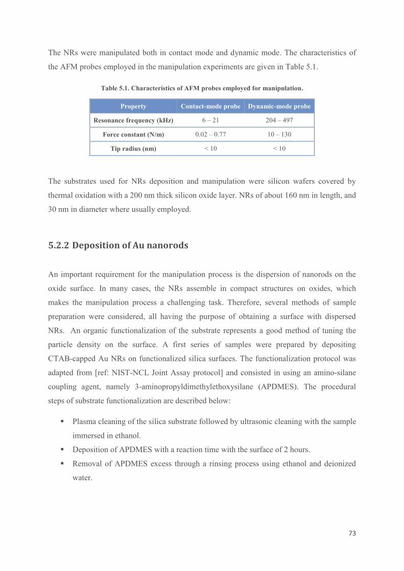
73
The NRs were manipulated both in contact mode and dynamic mode. The characteristics of
the AFM probes employed in the manipulation experiments are given in Table 5.1.
Table 5.1. Characteristics of AFM probes employed for manipulation.
Property Contact-mode probe Dynamic-mode probe
Resonance frequency (kHz) 6 – 21 204 – 497
Force constant (N/m) 0.02 – 0.77 10 – 130
Tip radius (nm) < 10 < 10
The substrates used for NRs deposition and manipulation were silicon wafers covered by
thermal oxidation with a 200 nm thick silicon oxide layer. NRs of about 160 nm in length, and
30 nm in diameter where usually employed.
5.2.2 Deposition of Au nanorods
An important requirement for the manipulation process is the dispersion of nanorods on the
oxide surface. In many cases, the NRs assemble in compact structures on oxides, which
makes the manipulation process a challenging task. Therefore, several methods of sample
preparation were considered, all having the purpose of obtaining a surface with dispersed
NRs. An organic functionalization of the substrate represents a good method of tuning the
particle density on the surface. A first series of samples were prepared by depositing
CTAB-capped Au NRs on functionalized silica surfaces. The functionalization protocol was
adapted from [ref: NIST-NCL Joint Assay protocol] and consisted in using an amino-silane
coupling agent, namely 3-aminopropyldimethylethoxysilane (APDMES). The procedural
steps of substrate functionalization are described below:
§ Plasma cleaning of the silica substrate followed by ultrasonic cleaning with the sample
immersed in ethanol.
§ Deposition of APDMES with a reaction time with the surface of 2 hours.
§ Removal of APDMES excess through a rinsing process using ethanol and deionized
water.

74
§ Deposition of gold nanorods solution on the substrate and incubation in a humidified
chamber at room temperature (the incubation time is dependent on the size of the
employed nanoparticles).
§ Ethanol rinse followed by deionized water rinse, and drying in a stream of nitrogen.
In order to verify the distribution of NRs on functionalized samples we first performed
scanning electron microscopy (SEM) investigations. Figure 5.1 shows the difference between
NRs deposited on an unfunctionalized (left) and a functionalized (right) silicon oxide surface.
Nevertheless, a disadvantage of a functionalized surface is represented by the presence of
residual organic molecules all over the surface (i.e., CTAB ligands, and/or molecules used for
functionalization), this constituting an impediment for an easy manipulation. Moreover, as
shown in the inset from Figure 5.2 (a) when manipulation is performed in contact mode, the
tip induces irreversible transformation on the residual organic layer.
Figure 5.1. SEM images of two samples containing nanorods: Left – Au NRs deposited on
unfunctionalized silica surface. Right – Au NRs deposited on APDMES functionalized silica surface.
We have equally considered the elimination of the organic through substrate heating in
ultra-high vacuum. Although this procedure contributed to a certain "cleaning" of the surface,
the Au NRs were susceptible to thermal damage, presenting deformation after heat exposure
[inset in Figure 5.2 (b)].
An alternative for organic materials removal is by a chemical cleaning protocol applied after
the dry-out of the droplet containing the NRs. It consists in rinsing with ethanol, then with
deionized water rinse, and last dry with nitrogen. AFM topography image in Figure 5.2 (c)
reveals a pollutant-free surface and acceptable nanorod dispersion for a future manipulation
process.

75
Figure 5.2. AFM topography measurements on samples prepared after three different protocols. (a)
Image of silica surface after functionalization and deposition of NRs. Inset: Influence on the organic layer
after a NR manipulation in contact mode. (b) AFM image of Au NRs deposited on an unfunctionalized
silica surface. Inset: Deformation of Au NRs after heating for organic removal. (c) Topographic image of
Au NRs on an unfunctionalized silica surface subjected to an ethanol cleaning protocol after deposition.
5.2.3 Manipulation of NRs in dynamic mode
The dynamic mode manipulation was based on varying the probe oscillation amplitude and
controlling the feedback loop. In order to switch from imaging mode to manipulation mode,
both the oscillation amplitude setpoint and the reactivity of feedback control are gradually
reduced until a threshold for particle movement is reached. The feedback control is mainly
determined by two parameters, the integral gain (IG) and the proportional gain (PG),
respectively. While the variation of PG has a limited effect when switching from imaging
mode to manipulation mode, the IG coefficient has a high impact on controlling the
interaction between the AFM probe and the displaced object. Regarding the amplitude
setpoint, this is ultimately the parameter that controls the distance between the AFM tip and
the surface, and one must be careful when defining new values, in order to assure an
appropriate manipulation and, in the same time, a preservation of the tip apex.
Figure 5.3 illustrates the cantilever motion in dynamic mode. At macroscopic tip-surface
separations, when the tip is not interacting with the surface, the oscillation amplitude (A0) is at
a maximum value dictated by the piezo-driver excitation. At a constant driving frequency
(resonant frequency) the oscillation amplitude of the tip decreases as the tip approaches the
surface. For imaging, the amplitude setpoint is usually set at about 80% of the free amplitude,
and the feedback loop works to keep As constant during scanning. This is done by adjusting
the tip-surface distance with the Z-piezo. For low values of IG, this adjustment is no longer
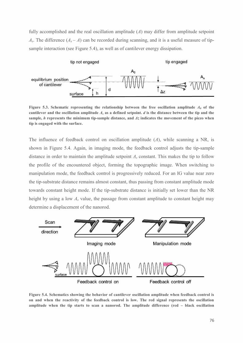
76
fully accomplished and the real oscillation amplitude (A) may differ from amplitude setpoint
As. The difference (As – A) can be recorded during scanning, and it is a useful measure of tip-
sample interaction (see Figure 5.4), as well as of cantilever energy dissipation.
Figure 5.3. Schematic representing the relationship between the free oscillation amplitude A0 of the
cantilever and the oscillation amplitude As as a defined setpoint. d is the distance between the tip and the
sample, h represents the minimum tip-sample distance, and Δz indicates the movement of the piezo when
tip is engaged with the surface.
The influence of feedback control on oscillation amplitude (A), while scanning a NR, is
shown in Figure 5.4. Again, in imaging mode, the feedback control adjusts the tip-sample
distance in order to maintain the amplitude setpoint As constant. This makes the tip to follow
the profile of the encountered object, forming the topographic image. When switching to
manipulation mode, the feedback control is progressively reduced. For an IG value near zero
the tip-substrate distance remains almost constant, thus passing from constant amplitude mode
towards constant height mode. If the tip-substrate distance is initially set lower than the NR
height by using a low As value, the passage from constant amplitude to constant height may
determine a displacement of the nanorod.
Figure 5.4. Schematics showing the behavior of cantilever oscillation amplitude when feedback control is
on and when the reactivity of the feedback control is low. The red signal represents the oscillation
amplitude when the tip starts to scan a nanorod. The amplitude difference (red – black oscillation

77
amplitude) is recorded as an image (see Figure 5.6 for instance), representing a good measure of tip
sample interaction change and a means towards the calculation of cantilever energy dissipation.
An additional way to control the nanomanipulation process is to correctly choose the scanning
area and the orientation of fast scan direction with respect to the manipulated object. Usually,
a perpendicular fast scan direction with respect to the NR long axis prevents the NR rotation.
Furthermore, an enhanced control of the displacement can be obtained if the nanorod is
positioned at the border of the scanning area (Figure 5.5). This is done by setting an offset on
the x direction of scanning area with respect to the initial position of the nanorod.
Figure 5.5. Schematic illustrating imaging mode and manipulation mode. For each case we present the
critical the scanning parameters (fast scan direction orientation, scanning angle, scanning area offset and
scan size). Blue arrow indicates the chosen displacement direction, while the designated position for the
nanorod after displacement is marked with X.
During manipulation the scan size is also reduced and thus there is less damage of the tip apex
(since feedback control is low). The displacement of the nanorod in the desired direction is
obtained by increasing the x offset with an increment lower than the diameter of the nanorod.
This is a very important aspect in our manipulation process. In Figure 5.5 we illustrate the
difference between setting parameters for imaging mode or for manipulation mode. As an
example, a first scan is performed at 1 x 1 μm in order to acquire a topographic image useful
for the identification of the initial position and orientation of the nanorod, and for setting the
trajectory and the final position. The next step consists in reducing the scan size to
200 x 200 nm, and changing the scan angle, in order to satisfy the condition of
perpendicularity between the fast scan direction and the long axis of the nanorod. By setting
the IG at the displacement threshold value we switch from imaging mode to manipulation
mode. Once the scan is completed we apply an x offset to the scan area. This step is repeated
as many times as necessary to cover the length of the designed trajectory.
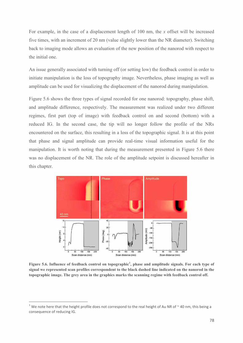
78
For example, in the case of a displacement length of 100 nm, the x offset will be increased
five times, with an increment of 20 nm (value slightly lower than the NR diameter). Switching
back to imaging mode allows an evaluation of the new position of the nanorod with respect to
the initial one.
An issue generally associated with turning off (or setting low) the feedback control in order to
initiate manipulation is the loss of topography image. Nevertheless, phase imaging as well as
amplitude can be used for visualizing the displacement of the nanorod during manipulation.
Figure 5.6 shows the three types of signal recorded for one nanorod: topography, phase shift,
and amplitude difference, respectively. The measurement was realized under two different
regimes, first part (top of image) with feedback control on and second (bottom) with a
reduced IG. In the second case, the tip will no longer follow the profile of the NRs
encountered on the surface, this resulting in a loss of the topographic signal. It is at this point
that phase and signal amplitude can provide real-time visual information useful for the
manipulation. It is worth noting that during the measurement presented in Figure 5.6 there
was no displacement of the NR. The role of the amplitude setpoint is discussed hereafter in
this chapter.
Figure 5.6. Influence of feedback control on topographic1, phase and amplitude signals. For each type of
signal we represented scan profiles correspondent to the black dashed line indicated on the nanorod in the
topographic image. The grey area in the graphics marks the scanning regime with feedback control off.
1 We note here that the height profile does not correspond to the real height of Au NR of ~ 40 nm, this being a
consequence of reducing IG.
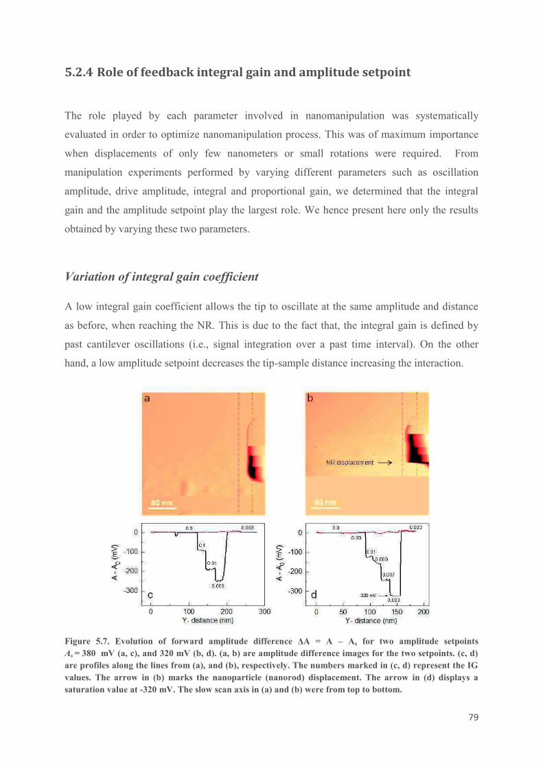
79
5.2.4 Role of feedback integral gain and amplitude setpoint
The role played by each parameter involved in nanomanipulation was systematically
evaluated in order to optimize nanomanipulation process. This was of maximum importance
when displacements of only few nanometers or small rotations were required. From
manipulation experiments performed by varying different parameters such as oscillation
amplitude, drive amplitude, integral and proportional gain, we determined that the integral
gain and the amplitude setpoint play the largest role. We hence present here only the results
obtained by varying these two parameters.
Variation of integral gain coefficient
A low integral gain coefficient allows the tip to oscillate at the same amplitude and distance
as before, when reaching the NR. This is due to the fact that, the integral gain is defined by
past cantilever oscillations (i.e., signal integration over a past time interval). On the other
hand, a low amplitude setpoint decreases the tip-sample distance increasing the interaction.
Figure 5.7. Evolution of forward amplitude difference ΔA = A – As for two amplitude setpoints
As = 380 mV (a, c), and 320 mV (b, d). (a, b) are amplitude difference images for the two setpoints. (c, d)
are profiles along the lines from (a), and (b), respectively. The numbers marked in (c, d) represent the IG
values. The arrow in (b) marks the nanoparticle (nanorod) displacement. The arrow in (d) displays a
saturation value at -320 mV. The slow scan axis in (a) and (b) were from top to bottom.
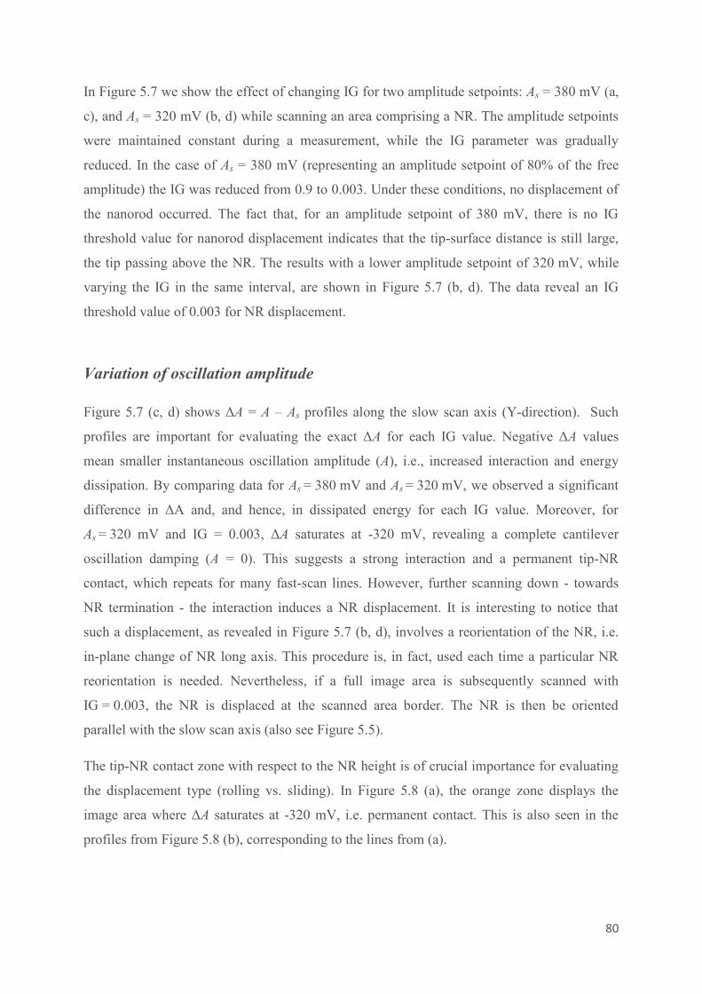
80
In Figure 5.7 we show the effect of changing IG for two amplitude setpoints: As = 380 mV (a,
c), and As = 320 mV (b, d) while scanning an area comprising a NR. The amplitude setpoints
were maintained constant during a measurement, while the IG parameter was gradually
reduced. In the case of As = 380 mV (representing an amplitude setpoint of 80% of the free
amplitude) the IG was reduced from 0.9 to 0.003. Under these conditions, no displacement of
the nanorod occurred. The fact that, for an amplitude setpoint of 380 mV, there is no IG
threshold value for nanorod displacement indicates that the tip-surface distance is still large,
the tip passing above the NR. The results with a lower amplitude setpoint of 320 mV, while
varying the IG in the same interval, are shown in Figure 5.7 (b, d). The data reveal an IG
threshold value of 0.003 for NR displacement.
Variation of oscillation amplitude
Figure 5.7 (c, d) shows ΔA = A – As profiles along the slow scan axis (Y-direction). Such
profiles are important for evaluating the exact ΔA for each IG value. Negative ΔA values
mean smaller instantaneous oscillation amplitude (A), i.e., increased interaction and energy
dissipation. By comparing data for As = 380 mV and As = 320 mV, we observed a significant
difference in ΔA and, and hence, in dissipated energy for each IG value. Moreover, for
As = 320 mV and IG = 0.003, ΔA saturates at -320 mV, revealing a complete cantilever
oscillation damping (A = 0). This suggests a strong interaction and a permanent tip-NR
contact, which repeats for many fast-scan lines. However, further scanning down - towards
NR termination - the interaction induces a NR displacement. It is interesting to notice that
such a displacement, as revealed in Figure 5.7 (b, d), involves a reorientation of the NR, i.e.
in-plane change of NR long axis. This procedure is, in fact, used each time a particular NR
reorientation is needed. Nevertheless, if a full image area is subsequently scanned with
IG = 0.003, the NR is displaced at the scanned area border. The NR is then be oriented
parallel with the slow scan axis (also see Figure 5.5).
The tip-NR contact zone with respect to the NR height is of crucial importance for evaluating
the displacement type (rolling vs. sliding). In Figure 5.8 (a), the orange zone displays the
image area where ΔA saturates at -320 mV, i.e. permanent contact. This is also seen in the
profiles from Figure 5.8 (b), corresponding to the lines from (a).
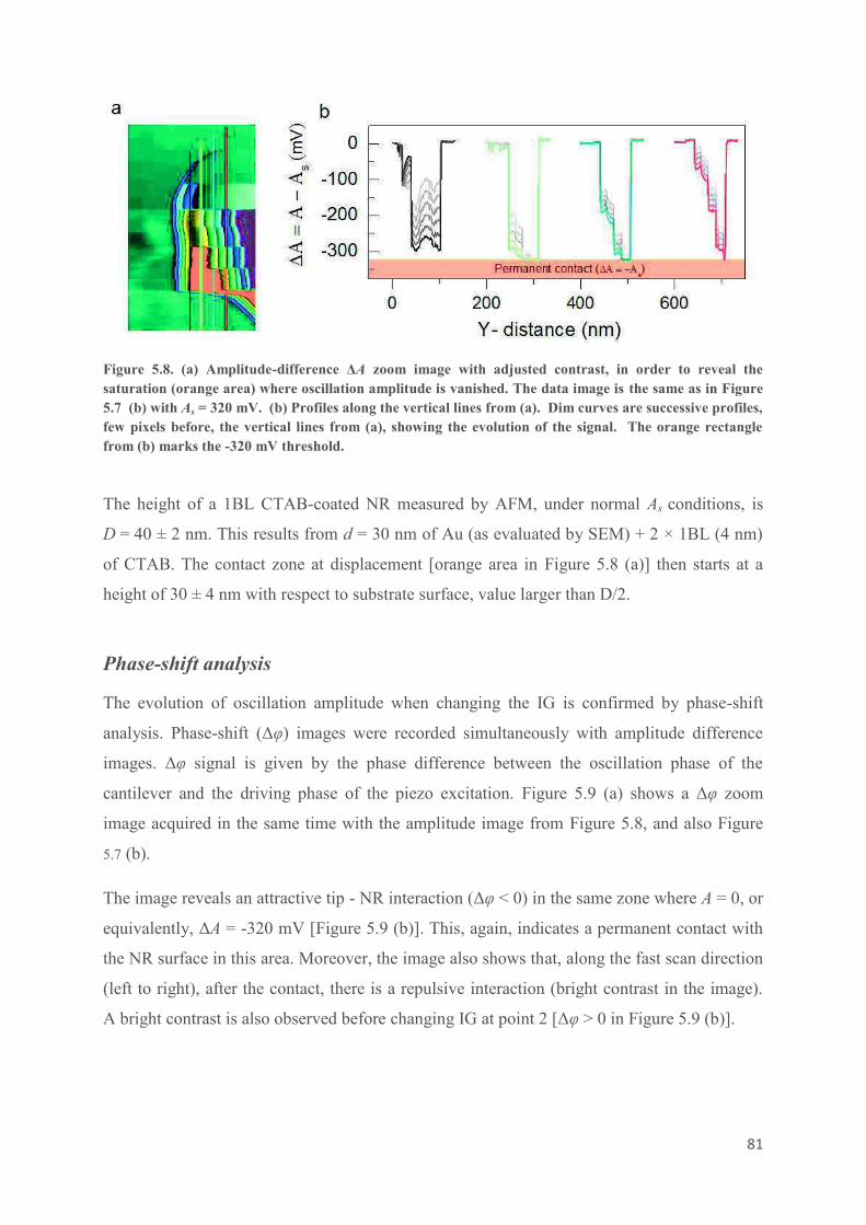
81
Figure 5.8. (a) Amplitude-difference ΔA zoom image with adjusted contrast, in order to reveal the
saturation (orange area) where oscillation amplitude is vanished. The data image is the same as in Figure
5.7 (b) with As = 320 mV. (b) Profiles along the vertical lines from (a). Dim curves are successive profiles,
few pixels before, the vertical lines from (a), showing the evolution of the signal. The orange rectangle
from (b) marks the -320 mV threshold.
The height of a 1BL CTAB-coated NR measured by AFM, under normal As conditions, is
D = 40 ± 2 nm. This results from d = 30 nm of Au (as evaluated by SEM) + 2 × 1BL (4 nm)
of CTAB. The contact zone at displacement [orange area in Figure 5.8 (a)] then starts at a
height of 30 ± 4 nm with respect to substrate surface, value larger than D/2.
Phase-shift analysis
The evolution of oscillation amplitude when changing the IG is confirmed by phase-shift
analysis. Phase-shift (Δφ) images were recorded simultaneously with amplitude difference
images. Δφ signal is given by the phase difference between the oscillation phase of the
cantilever and the driving phase of the piezo excitation. Figure 5.9 (a) shows a Δφ zoom
image acquired in the same time with the amplitude image from Figure 5.8, and also Figure
5.7 (b).
The image reveals an attractive tip - NR interaction (Δφ < 0) in the same zone where A = 0, or
equivalently, ΔA = -320 mV [Figure 5.9 (b)]. This, again, indicates a permanent contact with
the NR surface in this area. Moreover, the image also shows that, along the fast scan direction
(left to right), after the contact, there is a repulsive interaction (bright contrast in the image).
A bright contrast is also observed before changing IG at point 2 [Δφ > 0 in Figure 5.9 (b)].
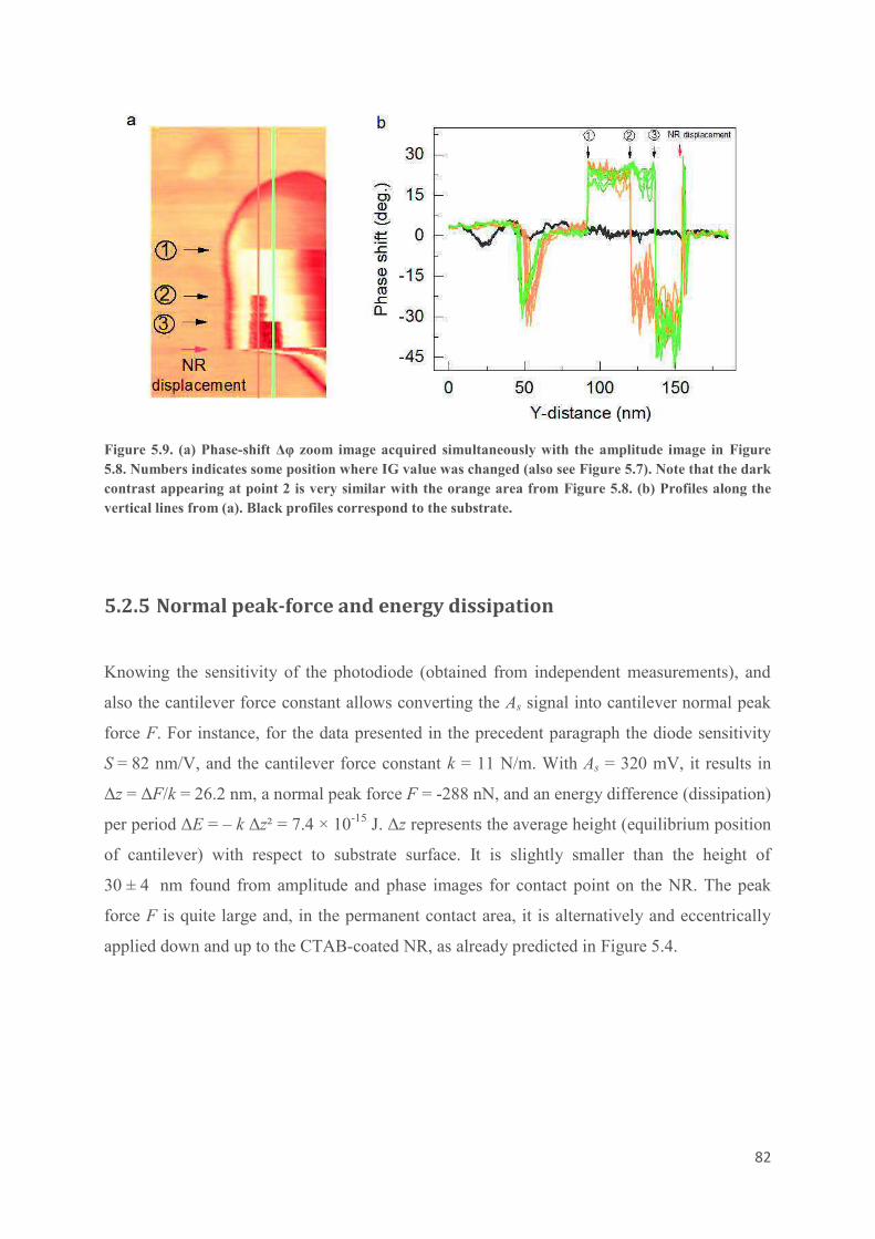
82
Figure 5.9. (a) Phase-shift Δφ zoom image acquired simultaneously with the amplitude image in Figure
5.8. Numbers indicates some position where IG value was changed (also see Figure 5.7). Note that the dark
contrast appearing at point 2 is very similar with the orange area from Figure 5.8. (b) Profiles along the
vertical lines from (a). Black profiles correspond to the substrate.
5.2.5 Normal peak-force and energy dissipation
Knowing the sensitivity of the photodiode (obtained from independent measurements), and
also the cantilever force constant allows converting the As signal into cantilever normal peak
force F. For instance, for the data presented in the precedent paragraph the diode sensitivity
S = 82 nm/V, and the cantilever force constant k = 11 N/m. With As = 320 mV, it results in
Δz = ΔF/k = 26.2 nm, a normal peak force F = -288 nN, and an energy difference (dissipation)
per period ΔE = – k Δz² = 7.4 × 10⁻¹⁵ J. Δz represents the average height (equilibrium position
of cantilever) with respect to substrate surface. It is slightly smaller than the height of
30 ± 4 nm found from amplitude and phase images for contact point on the NR. The peak
force F is quite large and, in the permanent contact area, it is alternatively and eccentrically
applied down and up to the CTAB-coated NR, as already predicted in Figure 5.4.
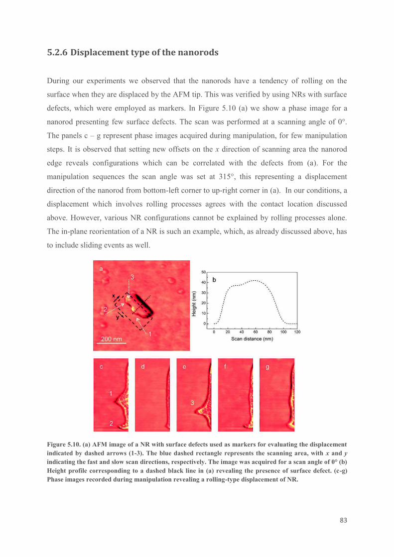
83
5.2.6 Displacement type of the nanorods
During our experiments we observed that the nanorods have a tendency of rolling on the
surface when they are displaced by the AFM tip. This was verified by using NRs with surface
defects, which were employed as markers. In Figure 5.10 (a) we show a phase image for a
nanorod presenting few surface defects. The scan was performed at a scanning angle of 0°.
The panels c – g represent phase images acquired during manipulation, for few manipulation
steps. It is observed that setting new offsets on the x direction of scanning area the nanorod
edge reveals configurations which can be correlated with the defects from (a). For the
manipulation sequences the scan angle was set at 315°, this representing a displacement
direction of the nanorod from bottom-left corner to up-right corner in (a). In our conditions, a
displacement which involves rolling processes agrees with the contact location discussed
above. However, various NR configurations cannot be explained by rolling processes alone.
The in-plane reorientation of a NR is such an example, which, as already discussed above, has
to include sliding events as well.
Figure 5.10. (a) AFM image of a NR with surface defects used as markers for evaluating the displacement
indicated by dashed arrows (1-3). The blue dashed rectangle represents the scanning area, with x and y
indicating the fast and slow scan directions, respectively. The image was acquired for a scan angle of 0° (b)
Height profile corresponding to a dashed black line in (a) revealing the presence of surface defect. (c-g)
Phase images recorded during manipulation revealing a rolling-type displacement of NR.
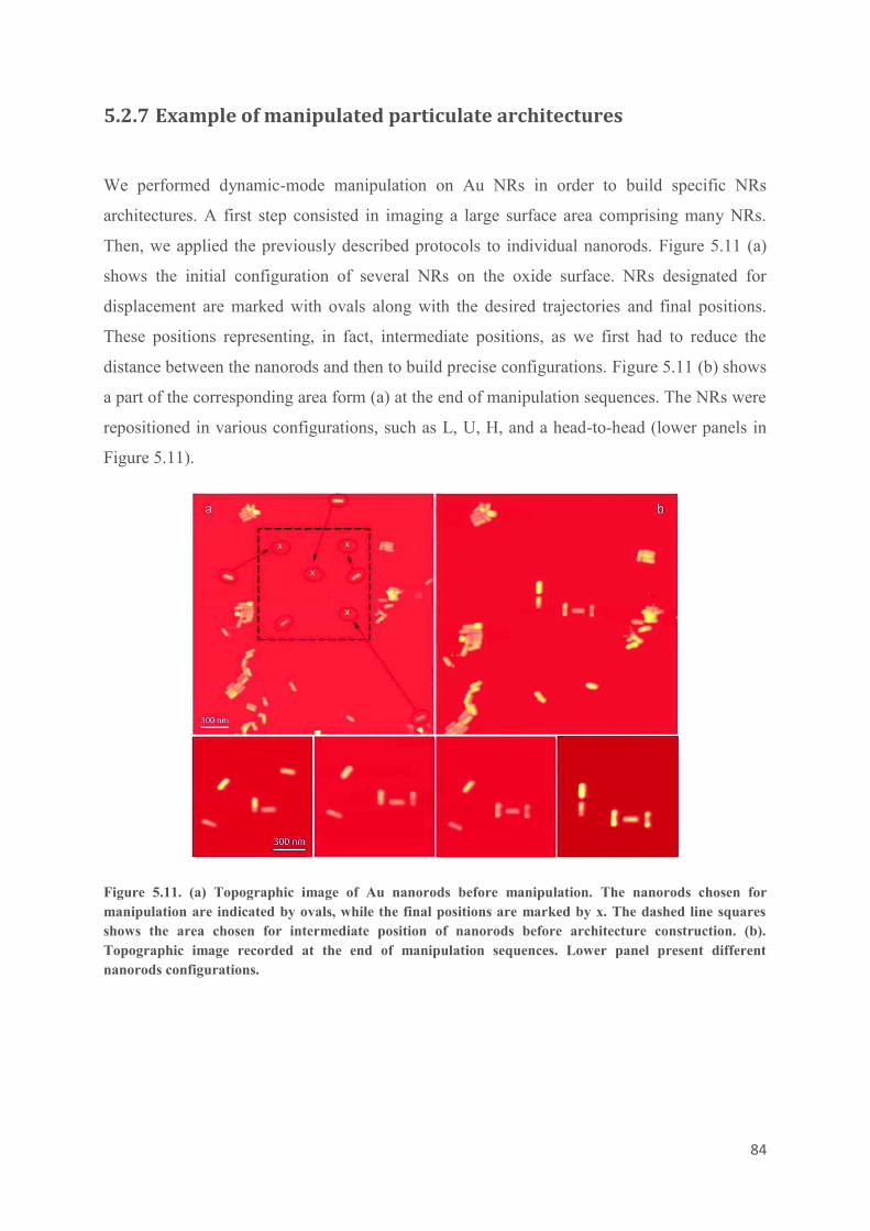
84
5.2.7 Example of manipulated particulate architectures
We performed dynamic-mode manipulation on Au NRs in order to build specific NRs
architectures. A first step consisted in imaging a large surface area comprising many NRs.
Then, we applied the previously described protocols to individual nanorods. Figure 5.11 (a)
shows the initial configuration of several NRs on the oxide surface. NRs designated for
displacement are marked with ovals along with the desired trajectories and final positions.
These positions representing, in fact, intermediate positions, as we first had to reduce the
distance between the nanorods and then to build precise configurations. Figure 5.11 (b) shows
a part of the corresponding area form (a) at the end of manipulation sequences. The NRs were
repositioned in various configurations, such as L, U, H, and a head-to-head (lower panels in
Figure 5.11).
Figure 5.11. (a) Topographic image of Au nanorods before manipulation. The nanorods chosen for
manipulation are indicated by ovals, while the final positions are marked by x. The dashed line squares
shows the area chosen for intermediate position of nanorods before architecture construction. (b).
Topographic image recorded at the end of manipulation sequences. Lower panel present different
nanorods configurations.

85
5.3 Conclusions
We performed AFM-based nanomanipulation of various gold nanorods, employing the AFM
either in dynamic or contact mode. In our case, the optimum conditions were provided by
dynamic mode. The protocols for dynamic-mode nanomanipulation were established by
performing series of manipulations while varying parameters such as amplitude setpoint, and
integral gain of the feedback control. This allowed us to predict and control the trajectory and
displacement of nanoparticles with high precision. We have built various nanoscale
particulate architectures which represent interesting prototypes for future AFM-based
absorption spectroscopy measurements described in next chapter.
86
References
[1] T. Junno, K. Deppert, L. Montelius and L. Samuelson, "Controlled manipulation of
nanoparticles with an atomic force microscope," Applied Physics Letters, vol. 66, p.
3627, 1995.
[2] A. A. G. Requicha, S. Meltzer, F. P. T. Arce, J. H. Makaliwe, H. Sikén, S. Hsieh, D. Lewis, B. E. Koel and M. E. Thompson, "Manipulation of nanoscale components with
the AFM: Principles and applications," in Proceedings of the 2001 1st IEEE Conference
on Nanotechnology. IEEE-NANO 2001, 2001.
[3] S. Hsieh, S. Meltzer, C. R. C. Wang, A. Requicha, M. E. Thompson and B. E. Koel,
"Imaging and manipulation of gold nanorods with an atomic force microscope," Journal
of Physical Chemistry B, vol. 106, p. 231, 2002.
[4] T. R. Ramachandran, C. Baur, A. Bugacov, A. Madhukar, B. E. Koel, A. Requicha and
C. Gazen , "Direct and controlled manipulation of nanometer-sized particles using the
non-contact atomic force microscope," Nanotechnology, vol. 9, p. 237, 1998.
[5] E. Gnecco, A. Rao, K. Mougin, G. Chandrasekar and E. Meyer, "Controlled
manipulation of rigid nanorods by atomic force microscopy," Nanotechnology, vol. 21, p.
215702, 2010.
[6] S. Kim, F. Shafiei, D. Ratchford and X. Li, "Controlled AFM manipulation of small
nanoparticles and assembly of hybrid nanostructures," Nanotechnology, vol. 2011, p.
115301, 2011.
[7] L. T. Hansen, A. Kühle, A. H. Sørensen, J. Bohr and P. E. Lindelof, "A technique for
positioning nanoparticles using an atomic force microscope," Nanotechnology, vol. 9, p.
337, 1998.
[8] P. A. Smith, C. D. Nordquist, T. N. Jackson and T. S. Mayer, "Electric-field assisted
assembly and alignment of metallic nanowires," Applied Physics Letters, vol. 77, p.
1399, 2000.
[9] B. F. Porter, L. Abelmann and H. Bhaskaran, "Design parameters for voltage-
controllable directed assembly of single nanoparticles," Nanotechnology, vol. 24, p.
405304, 2013.
[10] M. Tripathi, G. Paolicelli, S. D'Addato and S. Valeri, "Controlled AFM detachments and
movement of nanoparticles: gold clusters on HOPG at different temperatures,"
Nanotechnology, p. 245706, 2012.
87
[11] K. Xu, A. Kalantari and X. Qian, "Efficient AFM based nanoparticle manipulation via
sequential parallel pushing," IEEE Transactions on Nanotechnology, vol. 11, p. 666,
2012.
[12] D. Dietzel, C. Ritter, T. Mönninghoff, H. Fuchs, A. Schirmeisen and U. D. Schwarz, "Frictional duality observed during nanoparticle sliding," Physical Review Letters, vol.
101, p. 125505, 2008.
[13] E. Cihan, S. İpek, E. Durgun and M. Z. Baykara, "Structural lubricity under ambient conditions," Nature Communications, vol. 7, 2016.
[14] M. Sitti, "Atomic force microscope probe based controlled pushing for nanotribological
characterization," IEEE/ASME Transactions on mechatronics 9(2), p. 343, 2004.
[15] S. Darwich, K. Mougin, A. Rao, E. Gnecco, S. Jayaraman and H. Haidara, "Manipulation
of gold colloidal nanoparticles with atomic force microscopy in dynamic mode:
Influence of particle–substrate chemistry and morphology, and of operating conditions,"
Beilstein Journal of Nanotechnology, vol. 2, p. 85, 2011.
[16] A. M. Funston, C. Novo, T. J. Davis and P. Mulvaney, "Plasmon coupling of gold
nanorods at short distances and in different geometries," Nano Letters, vol. 9, p. 1651,
2009.

88
89
6 AFM force–based absorption spectroscopy
6.1 Introduction
Nowadays, there is no AFM force-based spectroscopic technique able to probe properties
such as light absorption in single nanoparticles or molecules. The first objective of this work
task, described in this chapter, was to prove that by detecting interaction forces with an AFM,
it was possible to measure photon absorption in visible and near infrared regimes on
nanoparticles deposited on surfaces. The idea is based on the optomechanical coupling of
photonic radiation pressure from the cavity formed by the AFM tip and a surface, with the
resonant modes of AFM cantilevers. High quality mechanical oscillators are known to couple
with electromagnetic fields above the zero-point fluctuations (see for instance [1]). Moreover,
recent experiments and theories conducted mostly with the purpose of cooling
micromechanical oscillators show an optomechanical coupling strong enough, to reach for
instance temperatures below 10 K. Our experiments and calculations performed with specific
parameters for our instrumentation and samples (light power, wavelength, cantilever
sensitivity, mirror reflectivity, NP absorption coefficients, etc.) show that the force sensitivity
of an in vacuo AFM microscope is largely sufficient to develop such a spectroscopy
technique. Several studies showed that the AFM can be adapted for optical force
measurements [2 5], but none with the purpose of performing NP absorption spectroscopy.
The optical cavity between an AFM plateau-tip and a surface is similar to a Fabry-Pérot
interferometer, provided that both are covered with a highly reflective material. A Fabry-Pérot
cavity, although of reduced dimensions, is still characterized by parameters such as photon
lifetime, cavity frequency, quality factor and cavity detuning. All these parameters play an
important role on the radiation pressure acting on the tip. Since the AFM tip can be vertically
displaced with a high precision by the Z-piezo, similar to the movable mirror from
Fabry-Pérot system, the photons inside the cavity can be coupled, for specific tip sample
distances, with the mechanical motion of the cantilever. The modification of resonant

90
frequencies due to radiation pressure is an effect of the coupling between optical and
mechanical resonances. We hereafter briefly introduce the essential parameters involved in
optomechanical effects relevant for an AFM configuration.
6.2 Cavity optomechanics
Research on cavity optomechanics deals with the coupling of an optical field to a mechanical
oscillator. As a highly interdisciplinary field, it opened new research avenues, with
remarkable results. For instance, light-induced forces in optical cavities allowed exploring
phenomena such as cooling [6 8] and regenerative oscillations [9, 10]. Moreover, cavity
optomechanics finds applications in numerous fields, from sensing, or information processing
to quantum physics [11 13].
In the next two sections of this chapter we discuss the optomechanical coupling between a
fixed and a movable mirror. We first discuss some properties of optical cavities [1],
highlighting the parameters relevant for the AFM microscope. Then, in order to describe the
detection regimes as a function of laser power, cantilever stiffness, and cavity detuning, we
describe calculations done with the specific parameters for our instrumentation.
6.2.1 Optical cavities
Optical cavities, also known as optical resonators, usually consist in two mirrors coated with
thin metallic films which present a high reflectance in the spectral interval of interest. In our
experiments, the cavity was formed by the space between an AFM plateau-tip and a high
reflective surface. In general, an optical cavity with the mirrors separated by a distance L,
contains a series of resonances which are given by:
IC@9E3 � '1 ×1w�� (6.1)
where, ωcav is the cavity resonance frequency, m is the resonance mode, and c is the speed of
light in vacuum. The free spectral range (FSR) of the cavity is given by the separation of two
resonances:
91
�I��� � 1w �� (6.2)
An important parameter is the optical finesse �, which depends on L, and corresponds to the
number of back-and-forth trajectories that a photon performs inside the cavity, on average.
The rate at which the photons escape from the cavity is given by k, which is the cavity decay
rate.
�1 � 1�I���a (6.3)
The cavity decay rate can also vary because photons are absorbed by the mirrors or other
species in the cavity. Optical finesse also depends on the reflectivity of the two mirrors, R1,
and R2. Thus, changing the reflectivity is similar to changing the absorption.
! � = 1w(MtM.)tb�� R sMtM. ! (6.4)
The photon lifetime τ is represented by the inverse of cavity decay rate, � = 1a$t and can be
used for determining the quality factor of the optical resonator, Q, which represents the mean
number of optical cycles for a photon.
�D`B =1IC@9� (6.5)
The cavity detuning Δ is another crucial parameter, and is given by the difference between
laser frequency ωL and cavity resonance frequency ωcav:
�1= 1I� R1IC@9 (6.6)
The average number of photons circulating inside the cavity can be obtained using
Equation 6.7, where P is the specific laser input power and H represents reduced Planck’s
constant.
m�C@9 =1 a*h�. 0 (a q)_ . 1 �HI� (6.7)
The reflection of the cavity can be determined using Equation 6.8 and can be used for
identifying the regime of cavity.
92
� =1 (aZ R1a*h) q R ��_(aZ 01a*h) q R ��_ (6.8)
The total decay rate k is defined by the sum between a decay rate due to input coupling, kex,
and one from internal losses, k0. Depending on the relationship between them, one can
determine the cavity regime. For instance, in the case of a*h � !a u !aZ the cavity is
overcoupled. A critical coupling is defined by aZ =1a*h. An undercoupled cavity is
encountered for a*h � aZ.
6.2.2 Optomechanical coupling and radiation-pressure force
In the case of a Fabry-Pérot cavity with a movable mirror the optomechanical coupling arises
by direct momentum transfer via light reflection. In the general case, radiation pressure is
induced when a photon reflection on a mirror transfers momentum to the mirror and, due to
momentum conservation, it generates a force. Considering its homogeneity on a given
surface, this action is considered as a pressure. For a periodic collision of a single photon with
a momentum � = 1HI� �_ and collision frequency f, the radiation force is given by [1]:
57@6 = q�r = qHI�� r (6.9)
In the presence of a cavity, the same photon will transfer momentum to the movable mirror
several times before leaving or being absorbed. In this case, the collision frequency will be
r = 1 � q�_ , where L is the cavity length. The radiation force and the number of photons
providing the intracavity field gives the radiation force inside the cavity:
57@6 =1HIC@9� �I� a(�).(a q_ ). (6.10)
In our case this force enters as a separate term in the equation of motion of the cantilever, and
can be used to simulate the resonant frequency response of the cantilever. However, detection
regimes and cantilever dynamics are most easily observable by analyzing the radiation
pressure potential in combination with the quadratic potential of the cantilever, in a very
similar way as for friction on oxides discussed in Chapter 3.
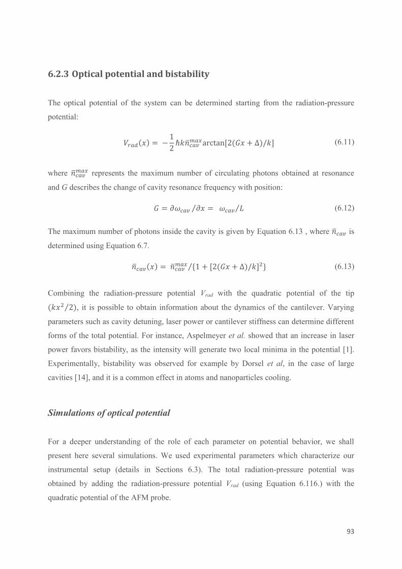
93
6.2.3 Optical potential and bistability
The optical potential of the system can be determined starting from the radiation-pressure
potential:
P7@6(-) = 1R�qHam�C@93@h ¡¢£ ¤1jq(¥- 0 �)bao (6.11)
where m�C@93@h represents the maximum number of circulating photons obtained at resonance
and G describes the change of cavity resonance frequency with position:
¥ = ^IC@91 ^-_ = 11IC@9 �_
(6.12)
The maximum number of photons inside the cavity is given by Equation 6.13 , where m�C@9 is
determined using Equation 6.7.
m�C@9(-) = 1m�C@93@h ¦� 0 jq(¥- 0 �)bao.§_ (6.13)
Combining the radiation-pressure potential Vrad with the quadratic potential of the tip
(a-. q_ ), it is possible to obtain information about the dynamics of the cantilever. Varying
parameters such as cavity detuning, laser power or cantilever stiffness can determine different
forms of the total potential. For instance, Aspelmeyer et al. showed that an increase in laser
power favors bistability, as the intensity will generate two local minima in the potential [1].
Experimentally, bistability was observed for example by Dorsel et al, in the case of large
cavities [14], and it is a common effect in atoms and nanoparticles cooling.
Simulations of optical potential
For a deeper understanding of the role of each parameter on potential behavior, we shall
present here several simulations. We used experimental parameters which characterize our
instrumental setup (details in Sections 6.3). The total radiation-pressure potential was
obtained by adding the radiation-pressure potential Vrad (using Equation 6.116.) with the
quadratic potential of the AFM probe.
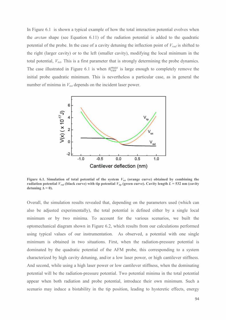
94
In Figure 6.1 is shown a typical example of how the total interaction potential evolves when
the arctan shape (see Equation 6.11) of the radiation potential is added to the quadratic
potential of the probe. In the case of a cavity detuning the inflection point of Vrad is shifted to
the right (larger cavity) or to the left (smaller cavity), modifying the local minimum in the
total potential, Vtot. This is a first parameter that is strongly determining the probe dynamics.
The case illustrated in Figure 6.1 is when m�C@93@h is large enough to completely remove the
initial probe quadratic minimum. This is nevertheless a particular case, as in general the
number of minima in Vtot depends on the incident laser power.
Figure 6.1. Simulation of total potential of the system Vtot (orange curve) obtained by combining the
radiation potential Vrad (black curve) with tip potential Vtip (green curve). Cavity length L = 532 nm (cavity
detuning Δ = 0).
Overall, the simulation results revealed that, depending on the parameters used (which can
also be adjusted experimentally), the total potential is defined either by a single local
minimum or by two minima. To account for the various scenarios, we built the
optomechanical diagram shown in Figure 6.2, which results from our calculations performed
using typical values of our instrumentation. As observed, a potential with one single
minimum is obtained in two situations. First, when the radiation-pressure potential is
dominated by the quadratic potential of the AFM probe, this corresponding to a system
characterized by high cavity detuning, and/or a low laser power, or high cantilever stiffness.
And second, while using a high laser power or low cantilever stiffness, when the dominating
potential will be the radiation-pressure potential. Two potential minima in the total potential
appear when both radiation and probe potential, introduce their own minimum. Such a
scenario may induce a bistability in the tip position, leading to hysteretic effects, energy
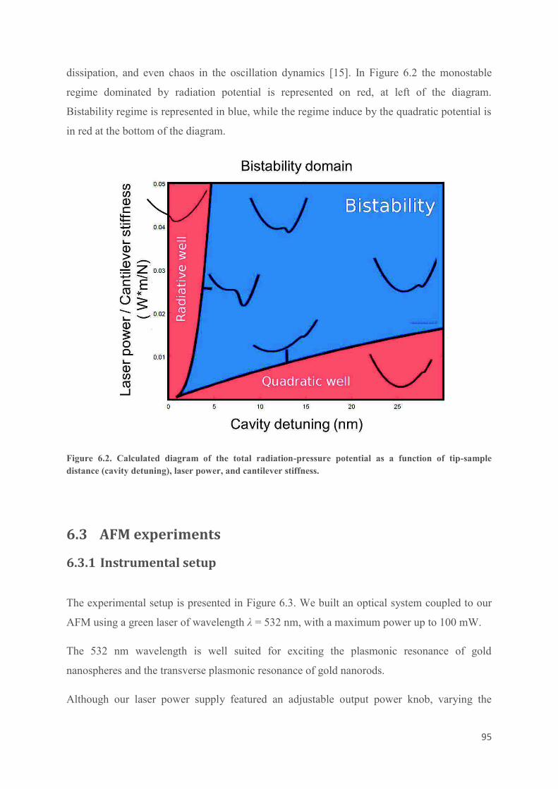
95
dissipation, and even chaos in the oscillation dynamics [15]. In Figure 6.2 the monostable
regime dominated by radiation potential is represented on red, at left of the diagram.
Bistability regime is represented in blue, while the regime induce by the quadratic potential is
in red at the bottom of the diagram.
Figure 6.2. Calculated diagram of the total radiation-pressure potential as a function of tip-sample
distance (cavity detuning), laser power, and cantilever stiffness.
6.3 AFM experiments
6.3.1 Instrumental setup
The experimental setup is presented in Figure 6.3. We built an optical system coupled to our
AFM using a green laser of wavelength λ = 532 nm, with a maximum power up to 100 mW.
The 532 nm wavelength is well suited for exciting the plasmonic resonance of gold
nanospheres and the transverse plasmonic resonance of gold nanorods.
Although our laser power supply featured an adjustable output power knob, varying the
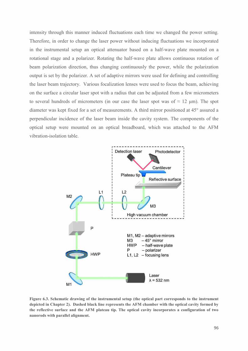
96
intensity through this manner induced fluctuations each time we changed the power setting.
Therefore, in order to change the laser power without inducing fluctuations we incorporated
in the instrumental setup an optical attenuator based on a half-wave plate mounted on a
rotational stage and a polarizer. Rotating the half-wave plate allows continuous rotation of
beam polarization direction, thus changing continuously the power, while the polarization
output is set by the polarizer. A set of adaptive mirrors were used for defining and controlling
the laser beam trajectory. Various focalization lenses were used to focus the beam, achieving
on the surface a circular laser spot with a radius that can be adjusted from a few micrometers
to several hundreds of micrometers (in our case the laser spot was of ≈ 12 μm). The spot
diameter was kept fixed for a set of measurements. A third mirror positioned at 45° assured a
perpendicular incidence of the laser beam inside the cavity system. The components of the
optical setup were mounted on an optical breadboard, which was attached to the AFM
vibration-isolation table.
Figure 6.3. Schematic drawing of the instrumental setup (the optical part corresponds to the instrument
depicted in Chapter 2). Dashed black line represents the AFM chamber with the optical cavity formed by
the reflective surface and the AFM plateau tip. The optical cavity incorporates a configuration of two
nanorods with parallel alignment.
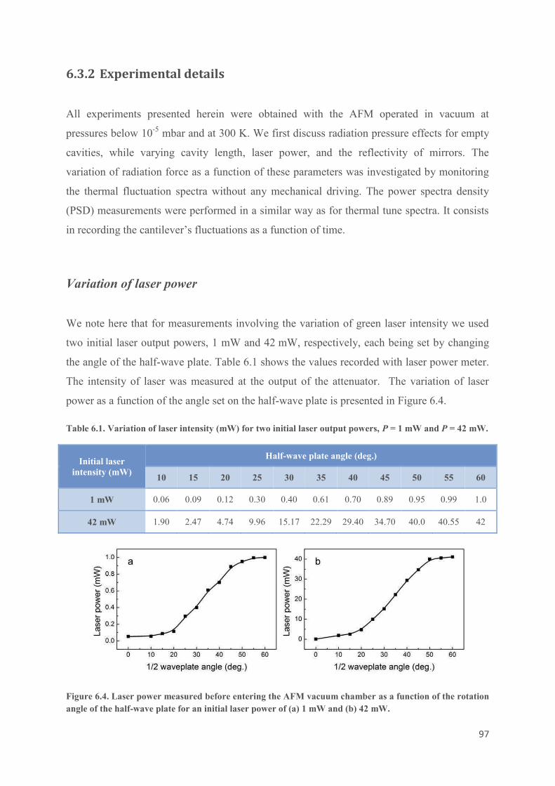
97
6.3.2 Experimental details
All experiments presented herein were obtained with the AFM operated in vacuum at
pressures below 10-5
mbar and at 300 K. We first discuss radiation pressure effects for empty
cavities, while varying cavity length, laser power, and the reflectivity of mirrors. The
variation of radiation force as a function of these parameters was investigated by monitoring
the thermal fluctuation spectra without any mechanical driving. The power spectra density
(PSD) measurements were performed in a similar way as for thermal tune spectra. It consists
in recording the cantilever’s fluctuations as a function of time.
Variation of laser power
We note here that for measurements involving the variation of green laser intensity we used
two initial laser output powers, 1 mW and 42 mW, respectively, each being set by changing
the angle of the half-wave plate. Table 6.1 shows the values recorded with laser power meter.
The intensity of laser was measured at the output of the attenuator. The variation of laser
power as a function of the angle set on the half-wave plate is presented in Figure 6.4.
Table 6.1. Variation of laser intensity (mW) for two initial laser output powers, P = 1 mW and P = 42 mW.
Initial laser
intensity (mW)
Half-wave plate angle (deg.)
10 15 20 25 30 35 40 45 50 55 60
1 mW 0.06 0.09 0.12 0.30 0.40 0.61 0.70 0.89 0.95 0.99 1.0
42 mW 1.90 2.47 4.74 9.96 15.17 22.29 29.40 34.70 40.0 40.55 42
Figure 6.4. Laser power measured before entering the AFM vacuum chamber as a function of the rotation
angle of the half-wave plate for an initial laser power of (a) 1 mW and (b) 42 mW.

98
Variation of cavity size and reflectivity
The optical cavity formed by the AFM probe and an Al-coated quartz surface was tuned
through Z-piezo displacement. At first, the tip was brought into contact with the surface (this
corresponded to a cavity of zero length), and then retracted to a desired distance. This was
done for each cantilever spectra measurement, in order to reduce uncontrolled drifts. Most of
the employed probes had tips with plateau configuration, with a diameter of ≈ 8 μm and
height of ≈ 15 μm [Figure 6.5 (a)]. The resonance frequency of the cantilever was around
10 kHz, with a force constant below 0.2 N/m. Cantilever’s length, width and thickness were
of 450 μm, 50 μm, and 2 μm, respectively. In Figure 6.5 (b) we depict schematics of cavities
considered in this chapter. If the NRs absorb a certain amount of photons, it is then expected
to observe a decrease in the radiation force exerted on the cantilever.
Figure 6.5. (a) SEM image of AFM cantilever with plateau tip [16]. (b) Schematics illustrating the optical
cavity formed by a reflective surface (S) and the AFM plateau tip (C). Frad represents the radiation force
acting on the cantilever, ntot is the total number of photons hitting the cavity, ¨©ª«¬ and ¨©ª«¬¬ indicate the
photon number circulating inside an empty cavity, and a cavity with nanorods, respectively.
For our initial experiments we considered enhancing the reflectivity coefficient of the plateau
tip through a sputtering deposition of aluminum this film, thus increasing cavity finesse.
Nevertheless, by depositing the aluminum thin film we changed the sensitivity of the
cantilever, thus diminishing the sensitivity when performing thermal tune. Figure 6.6 presents
two power spectral densities (PSD) of the cantilever probe before and after depositing the Al
coating. This is shown for two conditions, firstly with green laser off and secondly with green
laser at a power of 42 mW. The cavity length was of 532 nm in both measurements. PSD
spectra in Figure 6.6 reveal significant loss of force sensitivity in the case of a coated
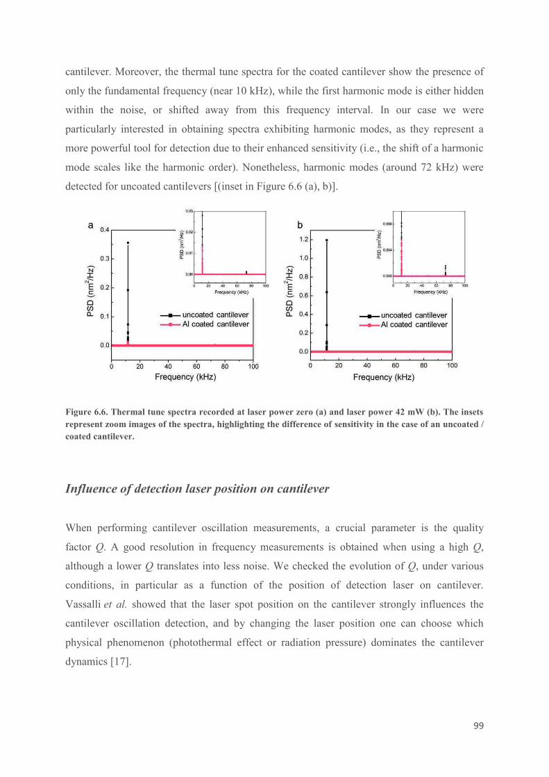
99
cantilever. Moreover, the thermal tune spectra for the coated cantilever show the presence of
only the fundamental frequency (near 10 kHz), while the first harmonic mode is either hidden
within the noise, or shifted away from this frequency interval. In our case we were
particularly interested in obtaining spectra exhibiting harmonic modes, as they represent a
more powerful tool for detection due to their enhanced sensitivity (i.e., the shift of a harmonic
mode scales like the harmonic order). Nonetheless, harmonic modes (around 72 kHz) were
detected for uncoated cantilevers [(inset in Figure 6.6 (a), b)].
Figure 6.6. Thermal tune spectra recorded at laser power zero (a) and laser power 42 mW (b). The insets
represent zoom images of the spectra, highlighting the difference of sensitivity in the case of an uncoated /
coated cantilever.
Influence of detection laser position on cantilever
When performing cantilever oscillation measurements, a crucial parameter is the quality
factor Q. A good resolution in frequency measurements is obtained when using a high Q,
although a lower Q translates into less noise. We checked the evolution of Q, under various
conditions, in particular as a function of the position of detection laser on cantilever.
Vassalli et al. showed that the laser spot position on the cantilever strongly influences the
cantilever oscillation detection, and by changing the laser position one can choose which
physical phenomenon (photothermal effect or radiation pressure) dominates the cantilever
dynamics [17].

100
Figure 6.7 shows the variation of the quality factor as a function of the detection laser position
on the cantilever. These results were obtained by recording and analyzing thermal tune
spectra, performed with a cavity length of 532 nm and under two green laser regimes, first
with green laser power off and secondly with green laser set at its maximum value. Quality
factor values were obtained for fundamental frequency [(a) in Figure 6.7], but also for the
harmonic mode [(b) in Figure 6.7], using � = 1r7 r_ , where fr is the resonant frequency and
Δf the resonance width.
Figure 6.7. (a) Variation of quality factor for different positions of the detection laser on the cantilever in
the case of (a) fundamental frequency f = 11.48 kHz and (b) harmonic mode f =72.85 kHz.
The coordinates indicated on x axis in Figure 6.7 represent the various positions of the
detection laser on cantilever which are schematically represented in Figure 6.8 (a). Changing
the laser position from the free end (pos1) of the cantilever towards the attached end (pos6)
induces a certain effect in cantilever dynamics. For instance, positioning the laser towards the
attached end of the cantilever impedes the detachment of the tip from the surface for a cavity
length of 532 nm and green laser off [Figure 6.7, pos6 in (a) and (b)]. Experimentally, this is
indicated by an absence of the fundamental frequency peak on the thermal tune spectra.
Similar, setting the laser to close to the free end of the cantilever obstructs the detection of
harmonic mode under a green laser regime. In our case, an optimal position for the detection
laser was between 3 and 4. The sensitivity of frequency measurements, namely the detection
of harmonics in the thermal tune spectra, is also dependent on the vibration modes of the
cantilever [Figure 6.8 (b)].

101
Figure 6.8. (a) Positions of detection laser on cantilever. (b) First three natural frequencies of the
cantilever.
Influence of green laser position on cantilever
Even though measurements were performed in high vacuum and particular precautions were
taken to achieve a high degree of measurement reproducibility, we also had to consider the
inherent drift and mechanical instability of the system (e.g., piezo drift, thermal expansion,
etc.). To see the impact of these factors, we tested spectra sensitivity to variations of the green
laser position on the tip, by displacing by a few microns the green laser spot on the cantilever
with respect to an initial position. Figure 6.9 shows as an example two optical images
displaying two green laser positions, which have been significantly spaced, in order to see a
clear image of the displacement. Data points presented in the right hand side of Figure 6.9
show a small a frequency shift induced by repositioning, but the effects are rather small of the
order of only few Hz at the maximum.
Figure 6.9. Frequency shift as a function of green laser position on cantilever. x1, x2, x3 represent three
positions for measurement conducted at 0.06 mW laser intensity, while g®¬ E g¬̄ E g°¬ are the same positions
for a laser intensity of 1 mW. The optical images show a green laser spot displaced with a larger extent, in
order to see a difference with the optical microscope. The laser is positioned on the plateau tip in the lower
image.
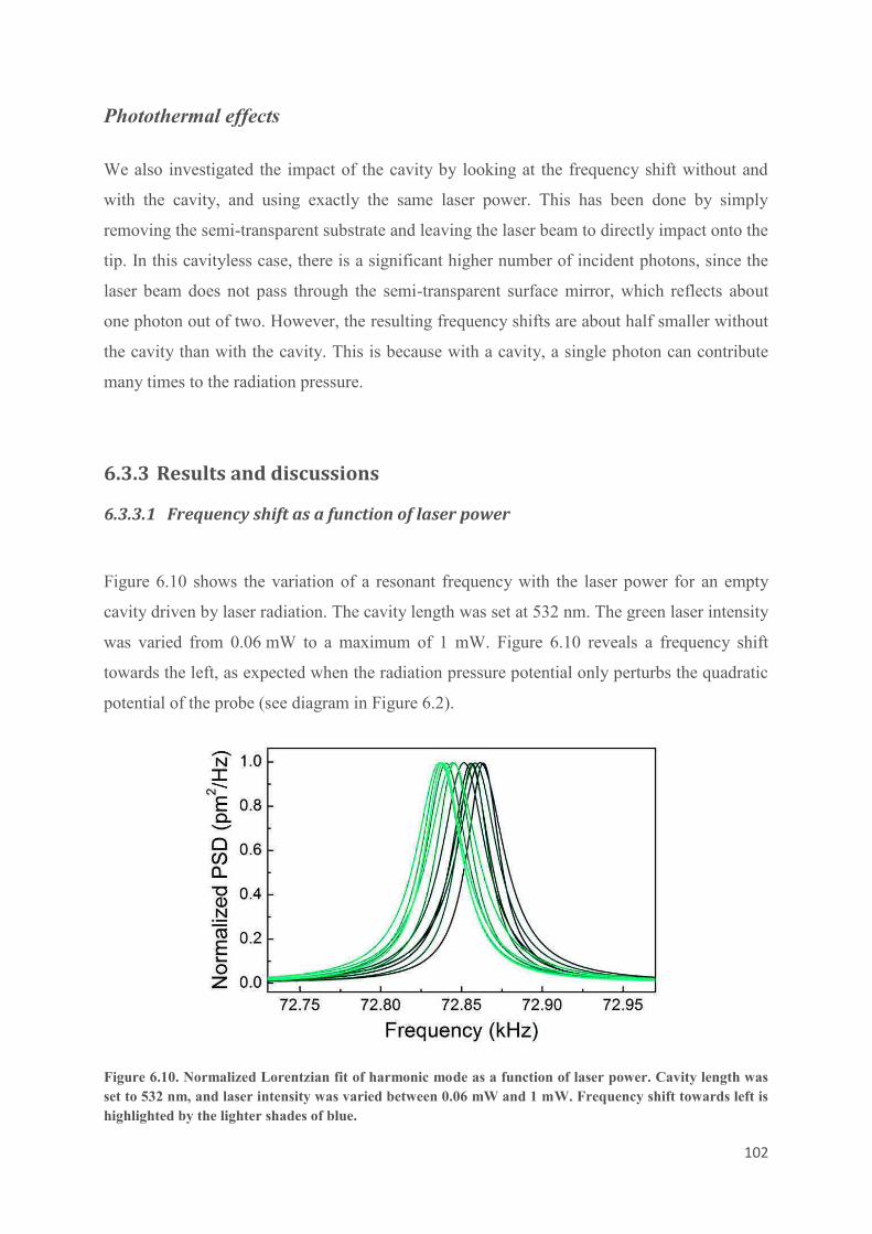
102
Photothermal effects
We also investigated the impact of the cavity by looking at the frequency shift without and
with the cavity, and using exactly the same laser power. This has been done by simply
removing the semi-transparent substrate and leaving the laser beam to directly impact onto the
tip. In this cavityless case, there is a significant higher number of incident photons, since the
laser beam does not pass through the semi-transparent surface mirror, which reflects about
one photon out of two. However, the resulting frequency shifts are about half smaller without
the cavity than with the cavity. This is because with a cavity, a single photon can contribute
many times to the radiation pressure.
6.3.3 Results and discussions
6.3.3.1 Frequency shift as a function of laser power
Figure 6.10 shows the variation of a resonant frequency with the laser power for an empty
cavity driven by laser radiation. The cavity length was set at 532 nm. The green laser intensity
was varied from 0.06 mW to a maximum of 1 mW. Figure 6.10 reveals a frequency shift
towards the left, as expected when the radiation pressure potential only perturbs the quadratic
potential of the probe (see diagram in Figure 6.2).
Figure 6.10. Normalized Lorentzian fit of harmonic mode as a function of laser power. Cavity length was
set to 532 nm, and laser intensity was varied between 0.06 mW and 1 mW. Frequency shift towards left is
highlighted by the lighter shades of blue.
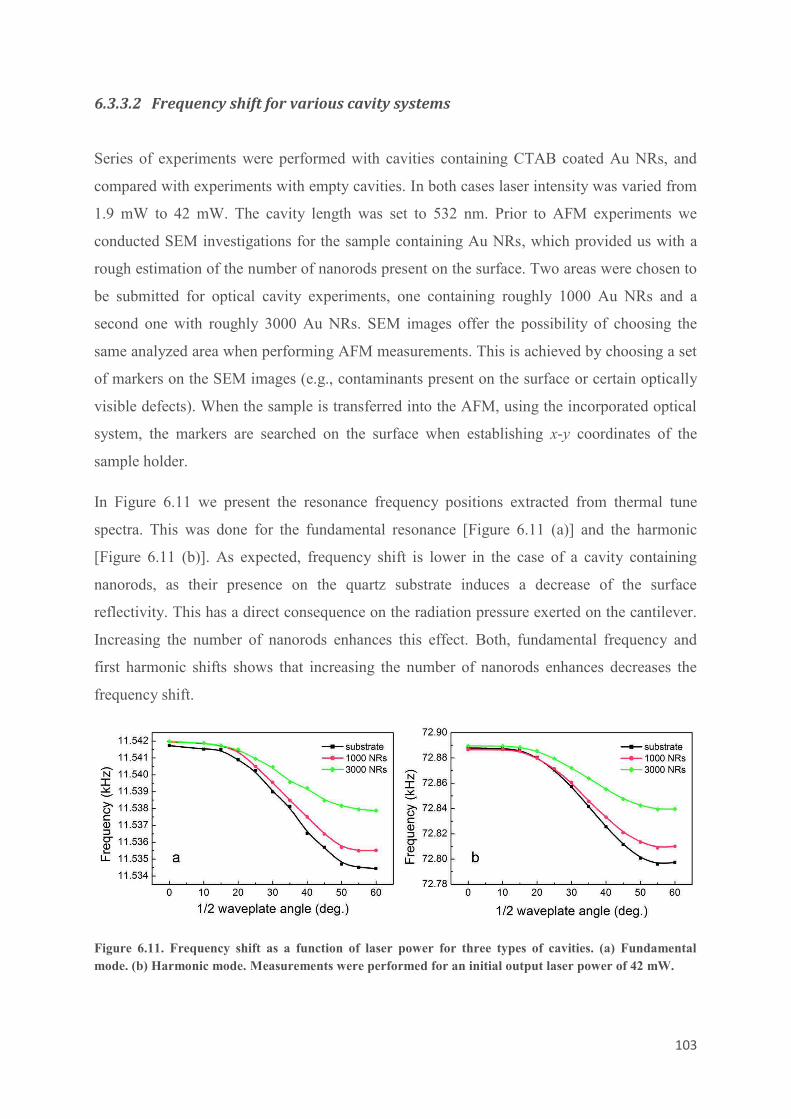
103
6.3.3.2 Frequency shift for various cavity systems
Series of experiments were performed with cavities containing CTAB coated Au NRs, and
compared with experiments with empty cavities. In both cases laser intensity was varied from
1.9 mW to 42 mW. The cavity length was set to 532 nm. Prior to AFM experiments we
conducted SEM investigations for the sample containing Au NRs, which provided us with a
rough estimation of the number of nanorods present on the surface. Two areas were chosen to
be submitted for optical cavity experiments, one containing roughly 1000 Au NRs and a
second one with roughly 3000 Au NRs. SEM images offer the possibility of choosing the
same analyzed area when performing AFM measurements. This is achieved by choosing a set
of markers on the SEM images (e.g., contaminants present on the surface or certain optically
visible defects). When the sample is transferred into the AFM, using the incorporated optical
system, the markers are searched on the surface when establishing x-y coordinates of the
sample holder.
In Figure 6.11 we present the resonance frequency positions extracted from thermal tune
spectra. This was done for the fundamental resonance [Figure 6.11 (a)] and the harmonic
[Figure 6.11 (b)]. As expected, frequency shift is lower in the case of a cavity containing
nanorods, as their presence on the quartz substrate induces a decrease of the surface
reflectivity. This has a direct consequence on the radiation pressure exerted on the cantilever.
Increasing the number of nanorods enhances this effect. Both, fundamental frequency and
first harmonic shifts shows that increasing the number of nanorods enhances decreases the
frequency shift.
Figure 6.11. Frequency shift as a function of laser power for three types of cavities. (a) Fundamental
mode. (b) Harmonic mode. Measurements were performed for an initial output laser power of 42 mW.

104
6.3.3.3 Influence of output laser power on frequency shift
Measurements have also been performed as a function of output laser power. Results are
plotted in Figure 6.12 and reveal an enhancement of frequency shift for increased output laser
powers. For both output laser powers, the frequency shift for the empty cavity is considerably
higher than for the cavity containing nanorods.
Figure 6.12. Mechanical resonant frequency as a function of laser power for empty and filled cavities. The
grey lines represent the two initial laser output powers, while the red dots and black squares indicate an
empty cavity and a cavity with Au NRs, respectively.
6.3.3.4 Influence of cavity detuning on frequency shift
The influence of different cavity lengths on the frequency response for empty cavities is an
additional interesting aspect, which helps defining further improvements of the technique. For
this, two sets of measurements were conducted, both of them on cavities incorporating Au
NRs and under a fixed green laser output power. For the first set we performed cavity
detuning from a cavity length of 66.5 nm and up to a cavity length of 3192 nm, with an
increment of 66.5 nm. As the green laser wavelength is of 532 nm, the applied increment
corresponds to ± ²_ . The second set was conducted from an initial cavity length of 14 nm and
up to a cavity length of 2506 n, this time with an increment of 14 nm (i.e., ± V²_ ).
Results are presented in Figure 6.13. Frequency shift curves present a similar profile for both
detuning regimes. In the first case [Figure 6.13 (a)] we observe a pronounced blue-shift of
frequency for cavity lengths inferior to ≈1170 nm, while for the second case the blue-shift
frequency stabilizes around 500 nm, in both cases the frequency shift showing a kind of

105
saturation for cavities larger than ≈1000 nm. These data demonstrates that smaller cavities
are more suitable, likely because of the larger fineness (larger photon lifetime). This is not
surprising in view of the 12° angle between the plateau tip and the surface. This angle is, in
certain circumstances, very useful because it allows an easy detachment of the tip from the
surface (reduced contact area), when measuring the zero cavity length.
Figure 6.13. Frequency shift as a function for cavity detuning for a cavity incorporating Au NRs. (a)
Cavity detuning from 66.5 nm to 3192 nm, with increment of 66.5 nm. (b) Cavity detuning from 14 nm to
2506 nm, with increment of 14 nm. Laser intensity was set at 40 mW in both cases.
6.4 Conclusions
Using sensitive AFM probes we detected changes in the radiation pressure. So far,
measurements performed in vacuum on empty cavities and on cavities incorporating gold
nanorods showed that absorption effects can be detected by this technique.
Metal nanoparticles, semiconductor quantum dots, or molecules, are known to absorb photons
at specific wavelengths. To obtaining an absorption spectrum, we need to illuminate the
sample with different laser wavelength. For each wavelength, the optical cavity must be
adapted, this causing a change of the cavity decay rate, hence change of the radiation force.
However, the change of k with the cavity length and light wavelength is a known variation.
Experimentally, the solution to at least a part of the problem comes from a feedback
regulation on one of the cavity modes, i.e. one peak of the Fabry-Pérot modes.
.

106
References
[1] M. Aspelmeyer, T. Kippenberg and F. Marquardt, "Cavity optomechanics," Review of
Modern Physics, vol. 86, p. 1391, 2014.
[2] D. R. Evans, P. Tayati, H. An, P. K. Lam, V. S. J. Craig and T. J. Senden, "Laser
actuation of cantilevers for picometre amplitude dynamic force microscopy," Scientific
Reports, vol. 4, p. 5567, 2014.
[3] D. Guan , Z. H. Hang, Z. Marcet, H. Liu, I. I. Kravchenko, C. T. Chan, H. B. Chan and P.
Tong, "Direct measurement of optical force induced by near-field plasmonic cavity using
dynamic mode AFM," Scientific Reports, vol. 5, 2015.
[4] D. Ma, J. L. Garrett and J. N. Munday, "Quantitative measurement of radiation pressure
on a microcantilever in ambient environment," Applied Physics Letters, p. 091107, 2015.
[5] F. Huang, V. A. Tamma, Z. Mardy, J. Burdett and H. K. Wickramasinghe, "Imaging
nanoscale electromagnetic near-field distributions using optical oorces," Scientific
Reports, vol. 5, p. 10610, 2015.
[6] C. H. Metzger and K. Karrai, "Cavity cooling of a microlever," Nature, vol. 432, p. 1002,
2004.
[7] O. Arcizet, P. F. Cohadon, T. Briant , M. Pinard and A. Heidmann, " Radiation-pressure
cooling and optomechanical instability of a micromirror," Nature, vol. 444, p. 71, 2006.
[8] A. Schleisser, P. Del'Haye, N. Nooshi, K. J. Vahala and T. J. Kippenberg, "Radiation
pressure cooling of a micromechanical oscillator using dynamical backaction," Physical
Review Letters, vol. 97, p. 243905, 2006.
[9] T. J. Kippenberg, H. Rokhsari, T. Carmon, A. Scherer and K. J. Vahala, "Analysis of
radiation-pressure induced mechanical oscillation of an optical microcavity," Physical
Review Letters, vol. 95, p. 033901, 2005.
[10] F. Marquardt, J. G. Harris and S. M. Girvin , "Dynamical multistability induced by
radiation pressure in high-finesse micromechanical optical cavities," Physical Review
Letters, vol. 96, p. 103901, 2006.
[11] K. Stannigel, P. Komar, S. J. M. Habraken, S. D. Bennett, M. D. Lukin, P. Zoller and P.
Rabl, "Optomechanical quantum information processing with photons and phonons,"
Physical Review Letters, vol. 109, p. 013603, 2012.
[12] W. Yu, W. C. Jiang, Q. Lin and T. Lu, "Cavity optomechanical spring sensing of single
molecules," Nature Communications, vol. 7, 2016.
107
[13] W. C. Jiang and Q. Lin, "Chip-scale cavity optomechanics in lithium niobate," Scientific
Reports, vol. 6, 2016.
[14] A. Dorsel, J. D. McCullen, P. Meystre and E. Vignes, "Optical bistability and mirror
confinement induced by radiation pressure," Physical Review Letters, vol. 51, no. 17, p.
1550, 1983.
[15] A. de Wijn, Chaos in systems with many degrees of freedom, PhD Thesis, Utrecht
University, ISBN 90-393-3868-X, 2004.
[16] NanoAndMore GmbH, "Plateau AFM tips," 2017. [Online]. Available:
https://www.nanoandmore.com/Plateau-Nanomechanics-AFM-Probes.html.
[17] M. Vassalli, V. Pini and B. Tiribilli, "Role of the driving laser position on atomic force
microscopy cantilevers excited by photothermal and radiation pressure effects," Applied
Physics Letters, vol. 97, p. 143105, 2010.

108
109
7 Summary and future perspectives
After a brief review on current importance of metal nanoparticles in various fields, we
introduced the great place that gold nanoparticles have in future plasmonic materials. Gold
nanoparticles also elicit a huge research activity in view of their applications in diagnostic,
therapy, drug, or gene delivery, sensing and imaging. There is hence a real interest in
understanding as quickly as possible, a large amount of chemical and physical properties of
these nanoparticles. New characterization techniques are nevertheless needed in order to
address new properties, which ask for constant improvement of the instrumentation. The main
research line discussed in this thesis was developed in this context. The modifications made
to our atomic force microscope were all conducted for increasing the resolution in
nanoparticle nanomanipulation and/or for detecting small variations of radiation-pressure
force due to photon absorption in particulate architectures.
We took a keen interest in fabricating well-controlled nanoparticle nanostructures by
employing the AFM as a high-precision manipulation tool. Prior to the development of the
nanomanipulation protocol, different studies regarding phenomena emerging at
sample-nanoparticle interface were performed. This was done to analyze the impact of the
various frictional factors on the nanomanipulation process.
We also described results regarding nanoscale friction on oxides, revealing an interesting
stick-slip friction mechanism characteristic for many oxide surfaces. Given that even metals
like aluminum show a native oxide layer at the surface, such a friction study was needed in
order to gain insight into the mechanism of displacing a nanoparticle on our surfaces.
However, our gold nanorods presented a capping molecular layer (CTAB), which we found
rather complicated to remove. A complementary layer-by-layer friction study was thus
conducted on CTAB thin films. We observed that depending on the number of layers at the
oxide surface, the presence of CTAB can either facilitate the manipulation process (acting as a
lubricant) or can constitute an impediment due to its plowing frictional properties.
110
Knowledge thus gained on friction mechanisms on oxide surfaces and CTAB multilayers
allowed us to develop a protocol for AFM dynamic-mode manipulation, which we
subsequently applied to obtain various nanoscale particulate architectures.
In Chapter 6 our focus was directed towards the capability of our instrumental setup to detect
the radiation-pressure forces emerging from a Fabry-Pérot-like cavity exposed to green laser
irradiation. The cavity was represented by the space between a plateau AFM tip and an
aluminum reflective surface. Thermal fluctuation spectra obtained under various experimental
conditions (cavity/no cavity, empty cavity/cavity with nanorods) revealed promising results.
We found a significant variation of cantilever oscillations as a function of different parameters
(e.g., laser power, cavity length, number of particles). An analysis of the frequency resonance
shift as a function of these parameters showed that our instrumental setup has indeed the
necessary sensitivity to detect weak changes in the radiation-pressure forces generated by
small variations of photon number inside the cavity.
There are several perspectives to this study, which may lead to an enhanced sensitivity, and
finally to single NRs resolution. Recent calculations performed in our group show that,
surprisingly, driving mechanically the cantilever to resonance, but at well-chosen amplitudes,
may compensate the small difference in photon lifetime due to absorption. This represents an
interesting perspective, which is currently tested, in our experimental setup.
In calculations, one way to simulate the presence of nanoparticles in a cavity is to decrease the
reflectivity of a mirror by an amount corresponding to absorbed photons. For a low number of
the particles of relatively low sizes, the physics of the optical cavity should not be drastically
modified. Experimental results revealed that with our current instrumental setup we can
estimate a minimum number of detectable NRs to about a few hundreds.
In addition to the future works mentioned above, there are two additional points to address for
a higher sensitivity. The first is to improve the cavity finesse by cutting the tips at particular
angles in order to increase the parallelism of the cavity (this is currently done by FIB). The
second is to increase even more the quality factor of cantilever resonances. One presently
explored way in this direction consists in the optomechanical cooling of the cantilever and a
concomitant optical driving. This is achieved by using an electro-optical modulation of the
cavity laser power. All these aspects are key factors for further development of the absorption
spectroscopy technique.

111
112
Publications and Conference contributions
Articles
1. Stochastic stick-slip nanoscale friction on oxide surfaces
A. D. Craciun, J. L. Gallani, and M. V. Rastei
Nanotechnology, vol. 27, p. 055402, 2016.
2. Thermal effects on van der Waals adhesive forces
V. Pinon, M. Wierez-Kien, A. D. Craciun, N. Beyer, J. L. Gallani, and M. V. Rastei
Physical Review B, vol. 93, p. 035424, 2016.
3. Nanoscale adhesion and sliding on biased semiconductors
A. Mukherjee, A. D. Craciun, J. L. Gallani, and M. V. Rastei
Faraday Discussions of the Royal Society of Chemistry, accepted 2017
4. Interface bonding in silicon oxide nanocontacts: interaction potentials and force
measurements
M. Wierez-Kien, A. D. Craciun, A. C. Pinon, S. Le Roux, J. L. Gallani, and M.V. Rastei
Physical Review B, under revision 2017
5. Nanoscale friction and adhesion of CTAB multilayers on oxide surfaces
A. D. Craciun, B. Donnio, J. L. Gallani and M. V. Rastei, in preparation (2017)
6. Nanomanipulation of CTAB-functionalized nanorods by atomic force microscopy
A. D. Craciun, B. Donnio, J. L. Gallani and M. V. Rastei, in preparation (2017)
7. Mechanically probing light absorption in gold nanorods with an AFM
A. D. Craciun, B. Donnio, J. L. Gallani and M. V. Rastei, in preparation (2017)
113
Conference contributions
Oral presentations
§ MP1303 COST Action "Understanding and Controlling Nano and Mesoscale Friction",
WG3 Workshop "Reversible Control of Surface Interactions", 2016, Oxford, UK
A. D. Craciun, B. Donnio, J. L. Gallani and M. V. Rastei
Friction and adhesion of CTAB Ultrathin Films Adsorbed on a Silicon Substrate
§ The Second European Workshop on Understanding and Controlling Nano and
Mesoscale Friction, 2016, Riga, Latvia
A. D. Craciun, J. L. Gallani and M. V. Rastei
Stochastic stick-slip nanoscale friction on oxide surfaces
§ DPG Berlin, 2015, Germany
A. D. Craciun, J. L. Gallani and M. V. Rastei
Stochastic stick-slip nanoscale friction on oxide surfaces
Poster presentations
§ The Second European Workshop on Understanding and Controlling Nano and Mesoscale
Friction, 2016, Riga, Latvia
A. D. Craciun, B. Donnio, J. L. Gallani and M. V. Rastei
Nanoscale friction and adhesion of CTAB multilayers on oxide surfaces
§ UFA – Winter school: Surface-Confined Synthesis of Nanostructures 2014, Baden-Baden,
Germany
A. D. Craciun, J. L. Gallani and M. V. Rastei
Sliding mechanics of nanoscale contacts

114
115
Extended abstract (in French)
Depuis quelques années une nouvelle classe de matériaux appelés métamatériaux, a ouvert un
champ de recherche nouveau et attirant. En raison de leurs propriétés intéressantes et
contre-intuitives, ces matériaux trouveront un jour de nombreuses applications [1-4]. Par
exemple, dans le cas des métamatériaux optiques qui sont basés sur des particules de métaux
nobles, l’exploitation des propriétés optiques uniques qui résultent de l'excitation des
résonances plasmon de particules nanométriques métalliques peut conduire à des avancées
significatives dans les domaines de l'optique, la photocatalyse, le traitement de l'information,
et développement de capteurs [5,6]. La possibilité d'adapter leurs propriétés provient du fait
que celles-ci sont étroitement liées à la structure interne, étant principalement déterminée par
la taille, la forme, la structure des blocs de construction ou de l'environnement. Bien qu'un
aspect important soit représenté par l'orientation des particules, ainsi que la distance
interparticulaire, les deux jouant un rôle crucial dans le contrôle des modes plasmoniques et la
réponse optique correspondante, il y a peu de recherches expérimentales en ce sens [6-11].
Plusieurs techniques offrent un moyen efficace pour la caractérisation de ces matériaux mais
un outil précis et puissant, capable de fournir un accès à la fois à l'architecture des
métamatériaux et aussi à des mesures directes des forces optiques en champ proche est
essentiel. Le microscope à force atomique (AFM) est un outil versatile pour effectuer des
investigations à l'échelle nanométrique. Grâce à sa sensibilité et sa haute résolution, il peut
être employé avec succès comme technique de nanomanipulation, car sa sonde à l'échelle
nanométrique peut être utilisée pour déplacer et orienter les particules sur des substrats, ce qui
permet de construire des nanostructures plasmoniques avec des géométries définies et de
régler précisément la distance interparticulaire. De plus, des études récentes ont montré que
l’AFM peut être adapté pour des mesures de force optique [12-14]. Ceci peut être réalisé en
couplant l'AFM à une cavité optique excitée par rayonnement laser, et mesurer les forces qui
agissent sur la sonde par détection de la déflection du levier.
116
Par conséquent, l'objectif principal de cette thèse était d'employer l'AFM d'abord comme un
outil de manipulation des nanoparticules sur des surfaces et ensuite comme une technique de
spectroscopie d’absorption.
La manipulation de nanoparticules (NPs) sur des surfaces, par AFM, exige une bonne
connaissance des différents processus hors équilibre impliqués dans la friction à l'échelle
nanométrique. La première partie de cette thèse a donc été consacrée à la compréhension des
paramètres pertinents pour la manipulation de nanoparticules, par exemple la force de friction,
le mécanisme de friction, l'énergie de liaison, les procédés de dissipation d'énergie, le rôle du
substrat. À cette fin, nous avons d'abord étudié le frottement se produisant à l'interface entre
une pointe nanométrique AFM et des substrats diélectriques. Un tel contact est similaire à ce
qui se passe pour les nanoparticules sur substrats. De ce fait, les surfaces diélectriques d'oxyde
nous sont apparues comme un bon choix car elles présentent une faible densité d'électrons,
assurant une bonne conservation des propriétés électroniques et optiques des NPs métalliques.
Nous avons abordé l'interaction de surface NP-oxyde à partir de deux approches différentes.
La première est basée sur l'idée d’une manipulation des NPs non fonctionnalisées. Dans ce
cas, les propriétés de glissement à l'échelle nanométrique ont été étudiées en analysant les
caractéristiques de frottement et d'adhérence d'un embout AFM sur diverses surfaces d'oxyde.
Ce type de contact est similaire à ce qui se passe pour les nanoparticules supportées, quand
aucun ligand organique n'est utilisé. La seconde approche concerne l'interface entre une
nanoparticule fonctionnalisée et un substrat oxyde.
Des expériences de friction effectuées sur diverses surfaces d'oxyde telles qu'une surface de
silicium avec une épaisseur de couche d'oxyde natif de 200 nm et de 3 nm, une surface
d'alumine et du verre ont révélé un nouveau mécanisme de friction nanométrique. La
Figure 1 (a) présente une image de friction enregistrée sur une surface de silice où on peut
remarquer l'impact marqué des processus de stick-slip.
La Figure 1 (b)-(e) montre des exemples de cycles de friction enregistrées pour les surfaces
d'oxyde susmentionnées. Tous les cycles sont caractérisés par des evenements de stick-slip à
l'échelle nanométrique inhomogènes. Les phases de ʺstickʺ ont néanmoins une pente similaire
pour une expérience donnée. Sur toutes ces surfaces, la séparation entre les phases ʺslipʺ
s'étend de quelques angstroms à plusieurs nanomètres sans aucune périodicité. Le caractère
stochastique des processus de stick-slip est robuste sur tous les oxydes étudiés pour des

117
vitesses de balayage allant jusqu'à plusieurs centaines de nm/s. Nous avons observé que la
vitesse à laquelle les événements de stick-slip commencent à disparaître dépend de la nature
de l'oxyde, de la pointe et de la charge.
Figure 1. a) Image de friction (balayage avant) montrant l'impact des processus de stick-slip. (b - e) Cycles
de friction pour différentes surfaces, comme indiqué sur chaque panneau. Vitesse de balayage: (a - d)
8 nm/s, (e) 3 nm/s. Les lignes noires et rouges correspondent aux analyses avant (gauche à droite) et
arrière (droite à gauche). Les crochets indiquent l'épaisseur d'oxyde. Les lignes obliques indiquent les
pentes des phases ʺstickʺ. Les phases ʺslipʺ sont les changements brusques du signal de friction.
Les mesures de frottement en fonction de la charge appliquée ont révélé un comportement
linéaire de frottement avec une force normale, indiquant la présence d'interactions adhésives
dispersives à l'interface. Les faibles forces d'arrachement, ainsi que les valeurs d'adhérence
obtenues par des mesures par spectroscopie de force, ont confirmé l'absence de liaisons
chimiques à courte distance à l'interface. Les mesures de frottement en fonction de la
température ont confirmé le rôle important joué par les effets thermiques dans le frottement
du contact d'aspérité simple et multiple, un effet direct de ceux-ci étant observé sur les profils

118
de frottement enregistrés aux basses vitesses comme des transitions aller-retour subies par la
pointe pendant un événement stick-slip.
Les résultats expérimentaux sont expliqués par un modèle de potentiel d’interaction de
Lennard-Jones modifié, qui considère une surface de contact discontinue et qui change après
chaque événement stick-slip [15,16]. Il est important de souligner que notre modèle est
valable dans le cas des surfaces rugueuses et pour des petits déplacements latéraux,
d’amplitude comparable au soulèvement de la pointe perpendiculairement à la surface. Ce
potentiel d'interaction est parfaitement adapté pour deux surfaces en interaction quand aucune
liaison chimique n’est créée à l'interface. Le modèle peut être utilisé pour expliquer la
formation et la fluctuation des événements stick-slip erratiques et peut fournir des
informations concernant l'impact des paramètres externes sur le frottement à l'échelle
nanométrique sur des surfaces d'oxyde. De plus, le modèle de potentiel d’interaction de
Lennard-Jones modifié corrélé avec la théorie de la vitesse de réaction peut fournir un cadre
théorique pour l'évaluation des paramètres microscopiques régissant l'adhésion à l'échelle
nanométrique [17].
P1(-E Q) = 1RSTUV WXYZ- [. R XYZ- [
\] (6)
où σ0 est la distance caractéristique d'équilibre pointe-échantillon, x est la coordonnée de
déplacement, et Δγ est le travail nécessaire pour induire un ʺslipʺ (glissement). Il est important
de mentionner ici que l'intégration de nombreux potentiels atomiques pour plusieurs couples
pointe-surface modifie le potentiel habituel de 6-12 LJ (typique pour les interactions
atomiques et moléculaires) dans une forme fonctionnelle 2-8, comme observé dans
l'équation 1. Cela se traduit par des régimes attractifs et répulsifs dépendants de la distance
plus grands. Pour les pointes et les surfaces rugueuses, lorsque le contact est
vraisemblablement établi par des aspérités, Δγ peut-être approximé par l'énergie adhésive.
C'est un paramètre qui s'adapte à la surface de contact et est a priori connu pour un matériau
donné. Pour la modélisation numérique, nous avons pris 1 × 10⁻¹⁹
J/nm2 (nous avons utilisé
Δγ = γ1 + γ2 avec γ1 = γ2 ≈ 50 mJ/m2 qui représente l'énergie de surface de la pointe et de
l'échantillon. Δγ dépend de la surface effective de contact S, que nous laissons varier après un
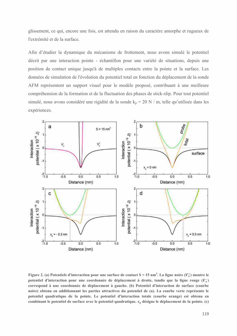
119
glissement, ce qui, encore une fois, est attendu en raison du caractère amorphe et rugueux de
l'extrémité et de la surface.
Afin d’étudier la dynamique du mécanisme de frottement, nous avons simulé le potentiel
décrit par une interaction pointe - échantillon pour une variété de situations, depuis une
position de contact unique jusqu'à de multiples contacts entre la pointe et la surface. Les
données de simulation de l'évolution du potentiel total en fonction du déplacement de la sonde
AFM représentent un support visuel pour le modèle proposé, contribuant à une meilleure
compréhension de la formation et de la fluctuation des phases de stick-slip. Pour tout potentiel
simulé, nous avons considéré une rigidité de la sonde kp = 20 N / m, telle qu’utilisée dans les
expériences.
Figure 2. (a) Potentiels d'interaction pour une surface de contact S = 15 nm2. La ligne noire (fg") montre le
potentiel d'interaction pour une coordonnée de déplacement à droite, tandis que la ligne rouge (fg$)
correspond à une coordonnée de déplacement à gauche. (b) Potentiel d'interaction de surface (courbe
noire) obtenu en additionnant les parties attractives du potentiel de (a). La courbe verte représente le
potentiel quadratique de la pointe. Le potentiel d'interaction totale (courbe orange) est obtenu en
combinant le potentiel de surface avec le potentiel quadratique. xp désigne le déplacement de la pointe. (c)

120
et (d) représentent l'évolution du potentiel d'interaction totale lors du déplacement de la pointe vers la
gauche (c) ou vers la droite (d) sur une distance de 0,3 nm.
En ce qui concerne les blocs constitutifs des nanostructures plasmoniques nous avons choisi
des nano-bâtonnets (nanorods) d’or (Au NRS) comme nano-objets pour la manipulation par
AFM, car leur anisotropie fournit des propriétés plasmoniques riches et ils offrent l'avantage
d'avoir deux modes de plasmon bien distincts. Un aspect important qui doit être pris en
considération est le surfactant utilisé pour la fonctionnalisation des Au NRs. Dans notre cas, il
s’agit du bromure de cetyltrimethylammonium (CTAB). Il a été montré que ce type d'agent
tensioactif ne peut être totalement éliminé de la surface des nanorods et son élimination totale
nécessite un procédé complexe et difficile à mettre en œuvre. Par conséquent, nous avons
effectué des mesures de frottement et d'adhésion sur CTAB adsorbées sur des surfaces de
silice [18], afin de déterminer son rôle dans la manipulation des Au NRs. A cet effet, plusieurs
échantillons contenant du CTAB ont été préparés. La topographie de la surface par AFM a
révélé l'organisation du CTAB par îlots de différentes hauteurs, formés de monocouches,
bicouches ou multicouches.
Figure 3. Image AFM en niveaux de gris (taille de balayage 2 x 2 μm) de films moléculaires CTAB
adsorbés sur la surface de silice (le gris foncé correspond à la surface de silice nue, tandis que les nuances

121
plus claires indiquent diverses épaisseurs de film CTAB). Image acquise en mode contact, sous vide
(pressions inférieures à 10-4
mbar), vitesse de balayage de 0,4 μm / s et force normale de -0,5 nN.
Nous avons alors remarqué un comportement de friction intéressant du CTAB dépendant de
l'interaction entre les couches [19], mais aussi fortement influencé par la variation de la force
appliquée lors des mesures de friction. Nous avons expliqué les résultats en utilisant un
modèle de frottement basé sur déformation locale moléculaire [20,21]. Notre étude a
également montré que le CTAB, lorsqu'il est adsorbé en une bicouche agit comme un
lubrifiant efficace à l'interface entre la surface et les Au NRs. Les propriétés lubrifiantes ainsi
dévoilées du CTAB ont donc été exploitées pour optimiser le processus de manipulation de
nanoparticules par AFM. Les études de frottement sur les multicouches CTAB permettent
également de comprendre que la nanomanipulation sur des couches CTAB épaisses est
probablement trop complexe pour une manipulation facile des Au NRs. Une seule bicouche
de CTAB à la surface des Au NRs apparaît alors comme une solution optimale, présentant un
double avantage: la lubrification et la propreté de la surface.
L'utilisation d'un microscope à force atomique comme outil de nanomanipulation a généré des
possibilités exceptionnelles pour la fabrication et l'étude d'architectures nanostructurées bien
contrôlées. En raison de la haute précision et de la résolution d'imagerie, un AFM peut être
utilisé pour déplacer latéralement des particules à l'échelle nanométrique sur diverses
surfaces. Le déplacement contrôlé de nanoparticules sur une surface peut être accompli de
différentes manières, y compris par des modes de fonctionnement par contact ou par vibration
(dynamique). Dans notre cas, les conditions optimales ont été fournies par le mode
dynamique. Par conséquent, les expériences de nanomanipulation ont été réalisées en mode
tapping, pour diverses raisons telles que: une résolution plus élevée est souvent réalisée à
l'aide des modes dynamiques, la préservation de la pointe AFM (par rapport au mode contact),
la présence de CTAB à la surface de Au NRs qui diminue les forces d'adhésion à l'interface
avec le substrat, ce qui rend difficile de manipuler en mode contact. Le protocole de
nanomanipulation a été élaboré en effectuant des séries de manipulations tout en faisant varier
des paramètres tels que l'amplitude d'oscillation ou la consigne d'amplitude, afin de
déterminer le rôle et l'impact de chacun sur le processus de nanomanipulation. Cela nous a
permis de prédire et de contrôler le déplacement des nanoparticules avec une grande
précision, et de construire diverses architectures de particules nanométriques pour des
mesures AFM de force optique en champ- proche.
122
Les expériences ont été réalisées dans des conditions de vide poussé et également dans des
conditions ambiantes. Les résultats n'ont pas révélé de différences qualitatives significatives
entre les expériences menées dans divers environnements. Néanmoins, le principal avantage
de réaliser des expériences à basse pression réside dans le fait que le déplacement des NRs est
plus facile (dissipation d'énergie de la sonde inférieure), ce qui se traduit finalement par une
préservation plus longue de la pointe.
La manipulation du mode dynamique était basée sur la variation de l'amplitude d'oscillation
de la sonde et le contrôle de la boucle de rétroaction. Afin de passer du mode d'imagerie au
mode de manipulation, la consigne d'amplitude d'oscillation et la réactivité du contrôle de
rétroaction sont progressivement réduites jusqu'au déplacement des particules. Le contrôle de
rétroaction est principalement déterminé par deux paramètres, le gain intégral (IG) et le gain
proportionnel (PG), respectivement. Alors que la variation de PG a un effet limité lors du
passage du mode d'imagerie au mode de manipulation, le coefficient IG a un impact élevé sur
le contrôle de l'interaction entre la sonde AFM et l'objet déplacé. En ce qui concerne la
consigne d'amplitude, c'est en définitive le paramètre qui contrôle la distance entre la pointe
de l'AFM et la surface, et il faut faire attention lors de la définition de nouvelles valeurs afin
d'assurer une manipulation appropriée et, dans le même temps, une préservation de l'apex de
la pointe.
Dans la dernière partie de la thèse l'accent a été mis sur l'emploi de l'AFM comme outil de
spectroscopie [Figure 4]. À cette fin, nous avons modifié notre microscope en le couplant à
une source laser (ʎ = 512 nm) et en focalisant le faisceau sur la partie inférieure du levier. La
cavité optique dans notre cas, similaire à un interféromètre de type Fabry-Pérot, a été formée
par l'espace entre une pointe d'AFM plate et d'une surface hautement réfléchissante, dans
lequel la pression de radiation peut être détectée par le levier. Une cavité Fabry-Pérot est
caractérisée par plusieurs paramètres, tels que la durée de vie des photons, la fréquence de la
cavité, le facteur de qualité et le désaccord de cavité. Tous ces paramètres jouent un rôle
important sur la pression de radiation agissant sur le levier. Étant donné que la pointe de
l'AFM, semblable au miroir mobile du système Fabry-Pérot, peut être déplacée verticalement,
les photons à l'intérieur de la cavité sont couplés avec le mouvement mécanique du levier. La
variation de la longueur de la cavité à cause de la pression de radiation est un effet de
couplage entre les résonances mécaniques et optiques. En utilisant des sondes AFM sensibles,
nous avons détecté des changements dans la pression de radiation, induite soit par la
puissance du laser ou par le désaccord de la cavité. Les mesures ont été effectuées sous vide
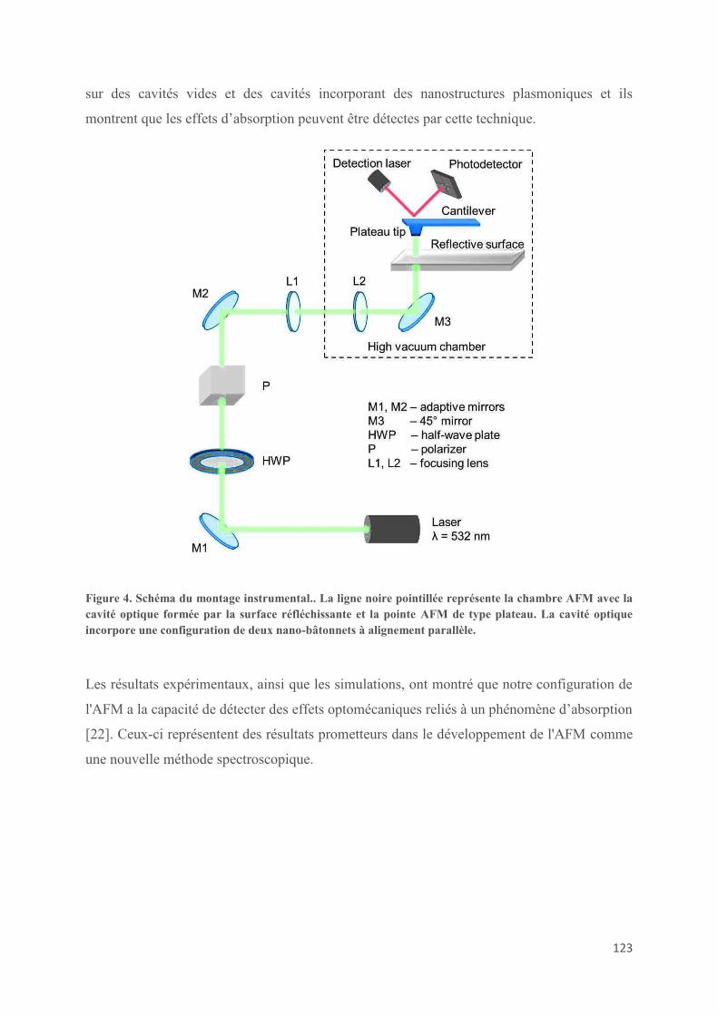
123
sur des cavités vides et des cavités incorporant des nanostructures plasmoniques et ils
montrent que les effets d’absorption peuvent être détectes par cette technique.
Figure 4. Schéma du montage instrumental.. La ligne noire pointillée représente la chambre AFM avec la
cavité optique formée par la surface réfléchissante et la pointe AFM de type plateau. La cavité optique
incorpore une configuration de deux nano-bâtonnets à alignement parallèle.
Les résultats expérimentaux, ainsi que les simulations, ont montré que notre configuration de
l'AFM a la capacité de détecter des effets optomécaniques reliés à un phénomène d’absorption
[22]. Ceux-ci représentent des résultats prometteurs dans le développement de l'AFM comme
une nouvelle méthode spectroscopique.
124
Références :
[1] See for instance: Metamaterials – Theory, design and applications, Ed. By T.J. Cui et al.,
Springer (2010)
[2] V.M. Shalaev, Nat. Photonics 1, 41 (2007)
[3] J. Valentine et al., Nature 455, 376 (2008)
[4] L. dal Negro, Nat. Mater. 13, 1080 (2014)
[5] K.Q. Le, J. Bai, J. Opt. Soc. Am. B. 32, 595 (2015)
[6] H. Chen et al., Chem. Soc. Rev. 42 , 2679 (2013)
[7] A. M. Funston et al., Nano Lett. 9, 1651 (2009)
[8] W. Zhang et al., Opt. Express 21, 172 (2013)
[9] G. Lu et al., Laser Photon. Rev. 1-8 (2015)
[10] H. Lange et al., Langmuir 28, 8862 (2012)
[11] D. Ratchford et al., Nano Lett. 11, 1049 (2011)
[12] Guan, Dongshi et al., Sci. Rep. 5, 16216 (2015)
[13] D.R. Evans et al., Sci. Rep. 4, 5567 (2014)
[14] D. Ma et al., Appl. Phys. Lett. 106, 091107 (2015)
[15] A.D. Craciun, J. L. Gallani and M. V. Rastei, Nanotechnology 27, 055402 (2016)
[16] M. Wierez-Kien, A. D. Craciun, A. C. Pinon, S. Le Roux, J. L. Gallani, and M. V.
Rastei, Nanotechnology, 29, 155704 (2018)
[17] A. V. Pinon, M. Wierez-Kien, A. D. Craciun, N. Beyer, J. L. Gallani, and M. V. Rastei,
Phys. Rev. B 93, 035424 (2016)
[18] A.D. Craciun, B. Donnio, J. L. Gallani and M. V. Rastei, in preparation
[19] A. M. Smith et al., J. Phys. Chem. 5, 4032-4037 (2014)
[20] M. Mishra et at., Tribol. Lett. 45, 417-426 (2012)
[21] C. Gauthier et al., Tribol, Int. 34, 469-479 (2001)
[22] A. D. Craciun et al., in preparation

125
126
Andra CRACIUN
AFM Force Spectroscopies of Surfaces and Supported Plasmonic
Nanoparticles
Résumé
Dans ce travail de thèse, le microscope à force atomique (AFM) a été utilisé comme outil de
manipulation de haute précision pour construire des nanostructures plasmoniques avec des
géométries définies et un réglage précis de la distance interparticulaire et également comme
technique de spectroscopie d'absorption. Différentes études concernant les phénomènes pertinents
pour la manipulation des nanoparticules et émergeant à l'interface substrat-nanoparticules, ont été
réalisées. Des expériences de frottement menées sur diverses surfaces d'oxydes ont révélé un
nouveau mécanisme de frottement à l’échelle nanométrique, expliqué par un modèle de potentiel
d'interaction de type Lennard-Jones modifié. Les propriétés de frottement et d'adhésion de CTAB
adsorbé sur silice sont également présentées. Des nano-bâtonnets d'or fonctionnalisés par du CTAB
ont été manipulés par AFM afin de construire des nanostructures plasmoniques. La dernière partie
de la thèse présente les efforts expérimentaux et théoriques pour démontrer la faisabilité de
l'utilisation d'un AFM comme une technique de spectroscopie optoélectronique à base de force.
Mots clés : microscopie à force atomique, nanoparticules plasmoniques, friction type stick-slip à l’échelle nanométrique, nano-bâtonnets d'or, AFM nanomanipulation, adsorption de CTAB sur des surfaces d'oxyde
Résumé en anglais
In this thesis work the atomic force microscope (AFM) was employed first as a high-precision
manipulation tool for building plasmonic nanostructures with defined geometries and precise tuning of
interparticle distance and second as an absorption spectroscopy technique. Different studies
regarding phenomena emerging at sample-nanoparticle interface relevant for nanoparticle
manipulation were performed. Friction experiments conducted on various oxide surfaces revealed a
novel nanoscale stick-slip friction mechanism, explained by a modified Lennard-Jones-like interaction
potential model. Frictional and adhesion properties of CTAB adsorbed on silica are also reported.
CTAB functionalized gold nanorods were used for building specific plasmonic particulate
nanostructures. The final part of the thesis presents experimental and theoretical efforts to
demonstrate the feasibility of using an AFM as a force-based optoelectronic spectroscopy technique.
Keywords : atomic force microscopy, plasmonic nanoparticles, nanoscale stick-slip friction, gold nanorods, AFM nanomanipulation, CTAB adsorption on oxide surfaces