cortex-m1 technical reference manual - arm...
TRANSCRIPT

Cortex™-M1Revision: r1p0
Technical Reference Manual
Copyright © 2006-2008 ARM Limited. All rights reserved.ARM DDI0413D
Cortex-M1Technical Reference Manual
Copyright © 2006-2008 ARM Limited. All rights reserved.
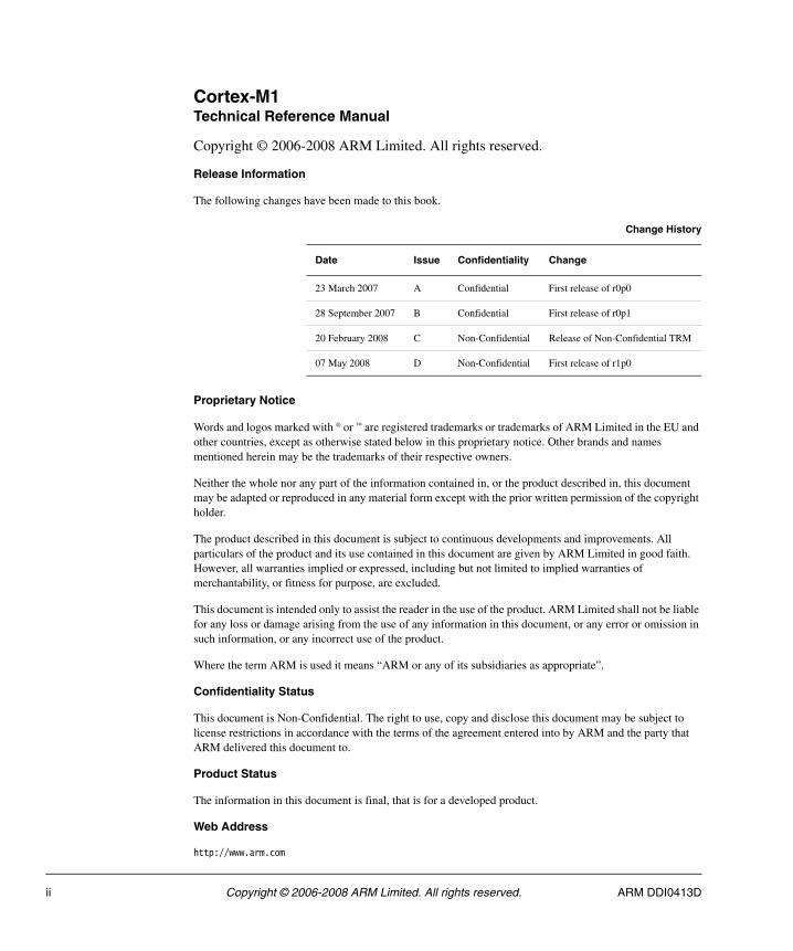
Release Information
The following changes have been made to this book.
Proprietary Notice
Words and logos marked with ® or ™ are registered trademarks or trademarks of ARM Limited in the EU and other countries, except as otherwise stated below in this proprietary notice. Other brands and names mentioned herein may be the trademarks of their respective owners.
Neither the whole nor any part of the information contained in, or the product described in, this document may be adapted or reproduced in any material form except with the prior written permission of the copyright holder.
The product described in this document is subject to continuous developments and improvements. All particulars of the product and its use contained in this document are given by ARM Limited in good faith. However, all warranties implied or expressed, including but not limited to implied warranties of merchantability, or fitness for purpose, are excluded.
This document is intended only to assist the reader in the use of the product. ARM Limited shall not be liable for any loss or damage arising from the use of any information in this document, or any error or omission in such information, or any incorrect use of the product.
Where the term ARM is used it means “ARM or any of its subsidiaries as appropriate”.
Confidentiality Status
This document is Non-Confidential. The right to use, copy and disclose this document may be subject to license restrictions in accordance with the terms of the agreement entered into by ARM and the party that ARM delivered this document to.
Product Status
The information in this document is final, that is for a developed product.
Web Address
http://www.arm.com
Change History
Date Issue Confidentiality Change
23 March 2007 A Confidential First release of r0p0
28 September 2007 B Confidential First release of r0p1
20 February 2008 C Non-Confidential Release of Non-Confidential TRM
07 May 2008 D Non-Confidential First release of r1p0
ii Copyright © 2006-2008 ARM Limited. All rights reserved. ARM DDI0413D

ContentsCortex-M1 Technical Reference Manual
PrefaceAbout this manual ........................................................................................ xivFeedback ..................................................................................................... xix
Chapter 1 Introduction1.1 About the processor .................................................................................... 1-21.2 Components, hierarchy, and implementation .............................................. 1-41.3 Configurable options ................................................................................. 1-101.4 About the architecture ............................................................................... 1-111.5 Binary compatibility with Cortex-M3 processor ......................................... 1-121.6 Product revisions ...................................................................................... 1-13
Chapter 2 Programmer’s Model2.1 About the programmer’s model ................................................................... 2-22.2 Registers ..................................................................................................... 2-42.3 Data types ................................................................................................. 2-102.4 Memory formats ........................................................................................ 2-112.5 Instruction set ............................................................................................ 2-13
Chapter 3 Memory Map3.1 About the memory map ............................................................................... 3-2
ARM DDI0413D Copyright © 2006-2008 ARM Limited. All rights reserved. iii

Contents
Chapter 4 Exceptions4.1 About the exception model ......................................................................... 4-24.2 Exception types .......................................................................................... 4-34.3 Exception priority ........................................................................................ 4-54.4 Stacks ......................................................................................................... 4-74.5 Pre-emption ................................................................................................ 4-84.6 Exception exit ........................................................................................... 4-104.7 Late-arrival ................................................................................................ 4-124.8 Exception control transfer ......................................................................... 4-134.9 Activation levels ........................................................................................ 4-144.10 Lock-up ..................................................................................................... 4-16
Chapter 5 Clocks and Resets5.1 About clocks and resets ............................................................................. 5-2
Chapter 6 System Control6.1 About system control .................................................................................. 6-26.2 System control register descriptions ........................................................... 6-4
Chapter 7 Nested Vectored Interrupt Controller7.1 About the NVIC ........................................................................................... 7-27.2 NVIC programmer’s model ......................................................................... 7-37.3 Level versus pulse interrupts ...................................................................... 7-97.4 Resampling level interrupts ...................................................................... 7-107.5 Interrupts as general purpose input .......................................................... 7-11
Chapter 8 Debug8.1 About debug ............................................................................................... 8-28.2 Debug control ............................................................................................. 8-58.3 ROM table ................................................................................................ 8-138.4 BPU .......................................................................................................... 8-168.5 DW unit ..................................................................................................... 8-198.6 Debug TCM interface ............................................................................... 8-248.7 Examples of debug register halt, access, and step .................................. 8-258.8 Data address watchpoint matching .......................................................... 8-288.9 Semiprecise watchpoints .......................................................................... 8-29
Chapter 9 Debug Access Port9.1 About the DAP ............................................................................................ 9-29.2 Debug access ............................................................................................. 9-39.3 AHB-AP ...................................................................................................... 9-5
Chapter 10 External and Memory Interfaces10.1 About bus interfaces ................................................................................. 10-210.2 External interface ...................................................................................... 10-3
iv Copyright © 2006-2008 ARM Limited. All rights reserved. ARM DDI0413D
Contents
10.3 Write buffer ............................................................................................... 10-410.4 Memory attributes ..................................................................................... 10-510.5 Memory interfaces .................................................................................... 10-6
Appendix A Signal DescriptionsA.1 Clocks and Resets ...................................................................................... A-2A.2 Miscellaneous ............................................................................................. A-3A.3 Interrupt interface ........................................................................................ A-4A.4 External AHB-Lite interface ......................................................................... A-5A.5 Memory interfaces ...................................................................................... A-6A.6 AHB-AP interface ........................................................................................ A-9
Glossary
ARM DDI0413D Copyright © 2006-2008 ARM Limited. All rights reserved. v

Contents
vi Copyright © 2006-2008 ARM Limited. All rights reserved. ARM DDI0413D

List of TablesCortex-M1 Technical Reference Manual
Change History ............................................................................................................. iiTable 1-1 Parameter configurable options .............................................................................. 1-10Table 1-2 Pin value configurable options ................................................................................ 1-10Table 2-1 Application Program Status Register bit functions .................................................... 2-6Table 2-2 Interrupt Program Status Register bit assignments .................................................. 2-7Table 2-3 EPSR bit assignments .............................................................................................. 2-8Table 2-4 Special-Purpose Priority Mask Register bit assignments .......................................... 2-9Table 2-5 Special-Purpose Control Register bit assignments ................................................... 2-9Table 2-6 Required mapping for an AHB-Lite interface .......................................................... 2-11Table 3-1 Processor memory regions ....................................................................................... 3-3Table 4-1 Exception types ......................................................................................................... 4-3Table 4-2 Exception scenarios .................................................................................................. 4-5Table 4-3 Exception entry steps ................................................................................................ 4-9Table 4-4 Exception exit steps ................................................................................................ 4-10Table 4-5 Exception return behavior ....................................................................................... 4-11Table 4-6 Transferring to exception processing ...................................................................... 4-13Table 4-7 Stack activation levels ............................................................................................. 4-14Table 4-8 Exception transitions ............................................................................................... 4-14Table 4-9 Exception subtype transitions ................................................................................. 4-15Table 6-1 System control registers ............................................................................................ 6-2Table 6-2 Auxiliary Control Register bit assignments ................................................................ 6-4Table 6-3 SysTick Control and Status Register bit assignments ............................................... 6-5Table 6-4 SysTick Reload Value Register bit assignments ....................................................... 6-7
ARM DDI0413D Copyright © 2006-2008 ARM Limited. All rights reserved. vii

List of Tables
Table 6-5 SysTick Current Value Register bit assignments ...................................................... 6-7Table 6-6 SysTick Calibration Value Register bit assignments ................................................ 6-8Table 6-7 CPUID Base Register bit assignments ..................................................................... 6-9Table 6-8 Interrupt Control State Register bit assignments .................................................... 6-10Table 6-9 Application Interrupt and Reset Control Register bit assignments ......................... 6-12Table 6-10 Configuration and Control Register bit assignments .............................................. 6-14Table 6-11 System Handler Priority Register 2 bit assignments ............................................... 6-15Table 6-12 System Handler Priority Register 3 bit assignments ............................................... 6-16Table 6-13 System Handler Control and State Register bit assignments ................................. 6-17Table 7-1 NVIC registers .......................................................................................................... 7-3Table 7-2 Interrupt Set-Enable Register bit assignments ......................................................... 7-4Table 7-3 Interrupt Clear-Enable Register bit assignments ...................................................... 7-5Table 7-4 Interrupt Set-Pending Register bit assignments ....................................................... 7-6Table 7-5 Interrupt Clear-Pending Registers bit assignments .................................................. 7-7Table 7-6 Interrupt Priority Registers 0-31 bit assignments ...................................................... 7-8Table 8-1 Core debug registers summary ................................................................................ 8-3Table 8-2 BPU register summary .............................................................................................. 8-3Table 8-3 DW register summary ............................................................................................... 8-4Table 8-4 Debug Fault Status Register bit assignments ........................................................... 8-6Table 8-5 Debug Halting Control and Status Register .............................................................. 8-8Table 8-6 Debug Core Register Selector Register ................................................................. 8-10Table 8-7 Debug Exception and Monitor Control Register ..................................................... 8-12Table 8-8 ROM memory ......................................................................................................... 8-13Table 8-9 Breakpoint Control Register bit assignments .......................................................... 8-17Table 8-10 Breakpoint Comparator Registers bit assignments ................................................ 8-18Table 8-11 DW Control Register bit assignments ..................................................................... 8-20Table 8-12 Control Register bit assignments ............................................................................ 8-20Table 8-13 DW Comparator Registers bit assignments ............................................................ 8-21Table 8-14 DW Mask Registers bit assignments ...................................................................... 8-22Table 8-15 DW Function Registers bit assignments ................................................................. 8-23Table 8-16 Settings for DW Function Registers ........................................................................ 8-23Table 9-1 Other AHB-AP ports ................................................................................................. 9-5Table 9-2 AHB access port registers ........................................................................................ 9-6Table 9-3 AHB-AP Control/Status Word Register bit assignments ........................................... 9-7Table 9-4 AHB-AP Transfer Address Register bit assignments ............................................... 9-8Table 9-5 AHB-AP Data Read/Write Register bit assignments ................................................ 9-9Table 9-6 Banked Data Register bit assignments ..................................................................... 9-9Table 9-7 ROM Address Register bit assignments ................................................................. 9-10Table 9-8 AHB-AP Identification Register bit assignments ..................................................... 9-10Table 10-1 HPROT[3:0] encoding ............................................................................................. 10-5Table 10-2 Byte-write size ........................................................................................................ 10-6Table 10-3 Instruction and Data TCM sizes .............................................................................. 10-7Table A-1 Reset signals ............................................................................................................ A-2Table A-2 Miscellaneous signals ............................................................................................... A-3Table A-3 Interrupt interface ...................................................................................................... A-4Table A-4 External AHB-Lite interface ...................................................................................... A-5Table A-5 ITCM interface .......................................................................................................... A-6
viii Copyright © 2006-2008 ARM Limited. All rights reserved. ARM DDI0413D
List of Tables
Table A-6 DTCM interface ......................................................................................................... A-6Table A-7 Debug ITCM interface ............................................................................................... A-7Table A-8 Debug DTCM interface ............................................................................................. A-7Table A-9 AHB-AP interface ...................................................................................................... A-9
ARM DDI0413D Copyright © 2006-2008 ARM Limited. All rights reserved. ix

List of Tables
x Copyright © 2006-2008 ARM Limited. All rights reserved. ARM DDI0413D

List of FiguresCortex-M1 Technical Reference Manual
Key to timing diagram conventions ............................................................................ xviFigure 1-1 Processor with debug block diagram ........................................................................ 1-4Figure 1-2 Processor block diagram ........................................................................................... 1-5Figure 2-1 Processor register set ............................................................................................... 2-4Figure 2-2 Application Program Status Register bit assignments .............................................. 2-6Figure 2-3 Interrupt Program Status Register bit assignments .................................................. 2-6Figure 2-4 Execution Program Status Register bit assignments ................................................ 2-7Figure 2-5 Special-purpose Priority Mask Register bit assignments .......................................... 2-8Figure 2-6 Special-Purpose Control Register bit assignments ................................................... 2-9Figure 3-1 Processor memory map ............................................................................................ 3-2Figure 4-1 Stack contents after a pre-emption ........................................................................... 4-8Figure 5-1 Reset signals ............................................................................................................. 5-2Figure 6-1 Auxiliary Control Register .......................................................................................... 6-4Figure 6-2 SysTick Control and Status Register bit assignments ............................................... 6-5Figure 6-3 SysTick Reload Value Register bit assignments ....................................................... 6-7Figure 6-4 SysTick Current Value Register bit assignments ...................................................... 6-7Figure 6-5 SysTick Calibration Value Register bit assignments ................................................. 6-8Figure 6-6 CPUID Base Register bit assignments ..................................................................... 6-9Figure 6-7 Interrupt Control State Register bit assignments .................................................... 6-10Figure 6-8 Application Interrupt and Reset Control Register bit assignments .......................... 6-12Figure 6-9 Configuration and Control Register bit assignments ............................................... 6-13Figure 6-10 System Handler Priority Register 2 bit assignments ............................................... 6-15Figure 6-11 System Handler Priority Register 3 bit assignments ............................................... 6-15
ARM DDI0413D Copyright © 2006-2008 ARM Limited. All rights reserved. xi

List of Figures
Figure 6-12 System Handler Control and State Register bit assignments ................................. 6-16Figure 7-1 Interrupt Priority Registers 0-7 bit assignments ........................................................ 7-8Figure 8-1 Debug Fault Status Register bit assignments ........................................................... 8-6Figure 8-2 Debug Halting Control and Status Register bit assignments .................................... 8-8Figure 8-3 Debug Core Register Selector Register bit assignments ....................................... 8-10Figure 8-4 Debug Exception and Monitor Control Register bit assignments ........................... 8-12Figure 8-5 Breakpoint Control Register bit assignments .......................................................... 8-16Figure 8-6 Breakpoint Comparator Registers bit assignments ................................................ 8-18Figure 8-7 DW Control Register bit assignments ..................................................................... 8-19Figure 8-8 DW Mask Registers 0-1 format ............................................................................... 8-21Figure 8-9 DW Function Registers bit assignments ................................................................. 8-22Figure 9-1 DAP configuration ..................................................................................................... 9-2Figure 9-2 AHB access port internal structure. .......................................................................... 9-5Figure 9-3 AHB-AP Control/Status Word Register bit assignments ........................................... 9-7Figure 9-4 AHB-AP Identification Register bit assignments ..................................................... 9-10Figure 10-1 ITCM write signal timings ........................................................................................ 10-6Figure 10-2 ITCM read signal timings ........................................................................................ 10-7
xii Copyright © 2006-2008 ARM Limited. All rights reserved. ARM DDI0413D

Preface
This preface introduces the Cortex-M1 r0p1 Technical Reference Manual (TRM). It contains the following sections:
• About this manual on page xiv
• Feedback on page xix.
ARM DDI0413D Copyright © 2006-2008 ARM Limited. All rights reserved. xiii
Preface
About this manual
This is the Technical Reference Manual (TRM) for the Cortex-M1 processor.
Product revision status
The rnpn identifier indicates the revision status of the product described in this manual, where:
rn Identifies the major revision of the product.
pn Identifies the minor revision or modification status of the product.
Intended audience
This manual is written to help:
• system designers, system integrators, and verification engineers who want to implement the processor in a Field-Programmable Gate Array (FPGA)
• software developers who want to use the processor in a FPGA.
Using this manual
This manual is organized into the following chapters:
Chapter 1 Introduction
Read this chapter for an introduction to the components of the processor and the processor instruction set.
Chapter 2 Programmer’s Model
Read this chapter for a description of the processor register set, modes of operation, and other information for programming the processor.
Chapter 3 Memory Map
Read this chapter for a description of the processor memory map.
Chapter 4 Exceptions
Read this chapter for a description of the processor exception model.
Chapter 5 Clocks and Resets
Read this chapter for a description of the processor clocking and resets.
Chapter 6 System Control
Read this chapter for a description of the registers and programmer’s model for system control.
xiv Copyright © 2006-2008 ARM Limited. All rights reserved. ARM DDI0413D
Preface
Chapter 7 Nested Vectored Interrupt Controller
Read this chapter for a description of the processor interrupt processing and control.
Chapter 8 Debug
Read this chapter for a description of the processor system debug components, and debugging and testing the processor.
Chapter 9 Debug Access Port
Read this chapter for a description of the processor debug access port and the Serial Wire JTAG Debug Port (SWJ-DP).
Chapter 10 External and Memory Interfaces
Read this chapter for a description of the processor bus interfaces.
Appendix A Signal Descriptions
Read this appendix for a summary of processor signals.
Glossary Read the Glossary for definitions of terms used in this manual.
Conventions
Conventions that this manual can use are described in:
• Typographical
• Timing diagrams on page xvi
• Signals on page xvi
• Numbering on page xvii.
Typographical
The typographical conventions are:
italic Highlights important notes, introduces special terminology, denotes internal cross-references, and citations.
bold Highlights interface elements, such as menu names. Denotes signal names. Also used for terms in descriptive lists, where appropriate.
monospace Denotes text that you can enter at the keyboard, such as commands, file and program names, and source code.
ARM DDI0413D Copyright © 2006-2008 ARM Limited. All rights reserved. xv

Preface
monospace Denotes a permitted abbreviation for a command or option. You can enter the underlined text instead of the full command or option name.
monospace italic Denotes arguments to monospace text where the argument is to be replaced by a specific value.
monospace bold Denotes language keywords when used outside example code.
< and > Enclose replaceable terms for assembler syntax where they appear in code or code fragments. For example:
MRC p15, 0 <Rd>, <CRn>, <CRm>, <Opcode_2>
Timing diagrams
The figure named Key to timing diagram conventions explains the components used in timing diagrams. Variations, when they occur, have clear labels. You must not assume any timing information that is not explicit in the diagrams.
Shaded bus and signal areas are undefined, so the bus or signal can assume any value within the shaded area at that time. The actual level is unimportant and does not affect normal operation.
Key to timing diagram conventions
Signals
The signal conventions are:
Signal level The level of an asserted signal depends on whether the signal is active-HIGH or active-LOW. Asserted means:
• HIGH for active-HIGH signals
Clock
HIGH to LOW
Transient
HIGH/LOW to HIGH
Bus stable
Bus to high impedance
Bus change
High impedance to stable bus
xvi Copyright © 2006-2008 ARM Limited. All rights reserved. ARM DDI0413D

Preface
• LOW for active-LOW signals.
Lower-case n Denotes an active-LOW signal.
Prefix H Denotes Advanced High-performance Bus (AHB) signals.
Prefix P Denotes Advanced Peripheral Bus (APB) signals.
Numbering
The numbering convention is:
<size in bits>'<base><number>
This is a Verilog method of abbreviating constant numbers. For example:
• 'h7B4 is an unsized hexadecimal value.
• 'o7654 is an unsized octal value.
• 8'd9 is an eight-bit wide decimal value of 9.
• 8'h3F is an eight-bit wide hexadecimal value of 0x3F. This is equivalent to b00111111.
• 8'b1111 is an eight-bit wide binary value of b00001111.
Additional reading
This section lists publications by ARM and by third parties.
See http://infocenter.arm.com/help/index.jsp for access to ARM documentation.
ARM publications
This manual contains information that is specific to the Cortex-M1 processor. See the following documents for other relevant information:
• ARMv6-M Architecture Reference Manual (ARM DDI 0419)
• ARMv6-M Instruction Set Quick Reference Guide (ARM QRC 0011)
• ARM AMBA® 3 AHB-Lite Protocol Specification (ARM IHI 0033)
• ARM CoreSight™ Components Technical Reference Manual (ARM DDI 0314)
• ARM Debug Interface v5, Architecture Specification (ARM IHI 0031)
• Application Binary Interface for the ARM Architecture (The Base Standard) (IHI0036)
• Cortex-M1 Configuration and Sign-off Guide (ARM DII 0166)
• Cortex-M1 Integration Manual (ARM DII 0167).
ARM DDI0413D Copyright © 2006-2008 ARM Limited. All rights reserved. xvii

Preface
Other publications
This section lists relevant documents published by third parties:
• IEEE Standard, Test Access Port and Boundary-Scan Architecture specification 1149.1-1990 (JTAG).
xviii Copyright © 2006-2008 ARM Limited. All rights reserved. ARM DDI0413D
Preface
Feedback
ARM welcomes feedback on the Cortex-M1 processor and its documentation.
Feedback on the processor
If you have any comments or suggestions about this product, contact your supplier giving:
• the product name
• a concise explanation of your comments.
Feedback on this manual
If you have any comments on this manual, send an email to [email protected] giving:
• the title
• the number
• the page number(s) to which your comments refer
• a concise explanation of your comments.
ARM also welcomes general suggestions for additions and improvements.
ARM DDI0413D Copyright © 2006-2008 ARM Limited. All rights reserved. xix

Preface
xx Copyright © 2006-2008 ARM Limited. All rights reserved. ARM DDI0413D

Chapter 1 Introduction
This chapter introduces the processor and instruction set. It contains the following sections:
• About the processor on page 1-2
• Components, hierarchy, and implementation on page 1-4
• Configurable options on page 1-10
• About the architecture on page 1-11
• Binary compatibility with Cortex-M3 processor on page 1-12
• Product revisions on page 1-13.
ARM DDI0413D Copyright © 2006-2008 ARM Limited. All rights reserved. 1-1
Introduction
1.1 About the processor
The processor is intended for deeply embedded applications that require a small processor integrated into an FPGA.
The processor incorporates:
• Processor core. This is a low gate count core that features:
— ARM architecture v6-M. A Thumb® Instruction Set Architecture (ISA) that also includes the 32-bit Thumb-2 BL, MRS, MSR, ISB, DSB, and DMB instructions.
— Operating System (OS) extension option. If this option is implemented, functionality within the processor is enabled that is capable of running an operating system. This includes the SVC instruction, a banked stack pointer register, and an integrated system timer.
— System exception model.
— Handler and Thread modes.
— Stack pointers. One stack pointer is always present.
If the OS extension option is implemented, two stack pointers are present.
— Thumb state only.
— ARM architecture v6-M style BE-8/LE support. Data endianness is configurable. Instructions and system control registers are always little-endian. If your processor has debug, debug resources and debugger accesses are always little-endian.
— No hardware support for unaligned accesses.
• Nested Vectored Interrupt Controller (NVIC). The NVIC is closely integrated with the processor to achieve low latency interrupt processing. Features include:
— the number of external interrupts that you can configure, 1, 8, 16 or 32
— fixed number of bits of priority, 2 bits, providing four levels of priority
— processor state automatically saved on interrupt entry and restored on interrupt exit, with no instruction overhead.
• Memory and external AHB-Lite interfaces.
• Optional full debug or reduced debug solutions that feature:
— debug access to all memory and registers in the system, including the processor register bank when the core is halted
— Debug Access Port (DAP)
— BreakPoint Unit (BPU) for implementing breakpoints
— Data Watchpoint (DW) unit for implementing watchpoints
1-2 Copyright © 2006-2008 ARM Limited. All rights reserved. ARM DDI0413D

Introduction
• 32-bit hardware multiplier. You can choose either the standard multiplier or a smaller, lower performance multiplier implementation.
ARM DDI0413D Copyright © 2006-2008 ARM Limited. All rights reserved. 1-3

Introduction
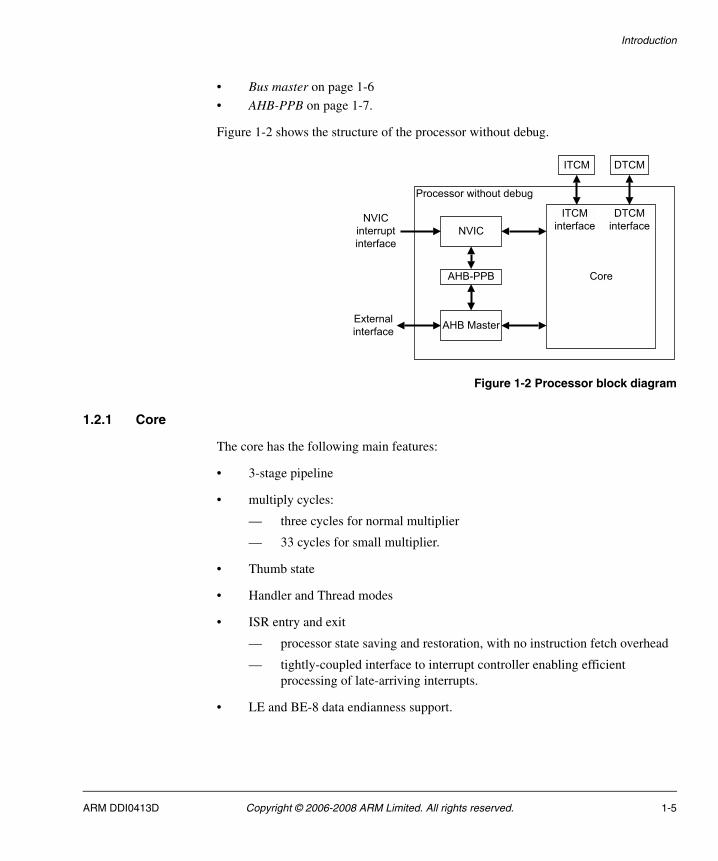
1.2 Components, hierarchy, and implementation
This section describes the components, hierarchy, and implementation of the processor with and without debug.
The main blocks of the processor with debug are:
• Core on page 1-5
• NVIC on page 1-6
• Bus master on page 1-6
• AHB-PPB on page 1-7
• Debug on page 1-7.
Figure 1-1 shows the structure of the processor with debug.
Figure 1-1 Processor with debug block diagram
The main blocks of the processor without debug are:
• Core on page 1-5
• Core memory interface on page 1-6
• NVIC on page 1-6
DTCM
NVIC
Processor with debug
ITCM
Debug subsystem
Breakpoint unit
AHB matrix
Debug TCM interface
AHB Decoder
AHB Multiplexer
AHB-PPB
CoreDbgData watchpoint unit
Debug control
ROM table
External AHB-Lite interface
NVIC Interrupt Interface
AHB master
SWJ-DP
AHB-APDAP
ITCM interface
DTCM interface
SW/JTAG interface
1-4 Copyright © 2006-2008 ARM Limited. All rights reserved. ARM DDI0413D
Introduction
• Bus master on page 1-6
• AHB-PPB on page 1-7.
Figure 1-2 shows the structure of the processor without debug.
Figure 1-2 Processor block diagram
1.2.1 Core
The core has the following main features:
• 3-stage pipeline
• multiply cycles:
— three cycles for normal multiplier
— 33 cycles for small multiplier.
• Thumb state
• Handler and Thread modes
• ISR entry and exit
— processor state saving and restoration, with no instruction fetch overhead
— tightly-coupled interface to interrupt controller enabling efficient processing of late-arriving interrupts.
• LE and BE-8 data endianness support.
DTCM
NVIC
Processor without debug
ITCM
AHB Master
AHB-PPB Core
External interface
NVIC interrupt interface
ITCM interface
DTCM interface
ARM DDI0413D Copyright © 2006-2008 ARM Limited. All rights reserved. 1-5

Introduction
Registers
The processor contains:
• 13 general purpose 32-bit registers.
• Link Register (LR).
• Program Counter (PC).
• Program Status Register, xPSR.
• Two banked SP registers. Without the OS extension option there is only one SP register present.
1.2.2 Core memory interface
Core access to Tightly-Coupled Memories (TCMs) is made exclusively through a dedicated core memory interface.
The core memory interface comprises:
• one core Instruction Tightly-Coupled Memory (ITCM) interface to access ITCM
• one core Data Tightly-Coupled Memory (DTCM) interface to access DTCM.
Because reads are speculatively fetched from TCMs, Device and Strongly-Ordered memory types are not supported, for example FIFOs in TCM space. You must ensure that any Flash memory in this space is tolerant of extra accesses at all times. The TCM interface does not support wait states.
1.2.3 NVIC
The NVIC is tightly coupled to the processor core. This facilitates low-latency exception processing. The main features include:
• a configurable number of external interrupts, 1, 8, 16, or 32
• a fixed number of bits of priority, 2 bits, providing four levels of configurable priority
• both level and pulse interrupt support
• processor state automatically saved on interrupt entry and restored on interrupt exit, with no instruction overhead.
See Chapter 7 Nested Vectored Interrupt Controller for more information.
1.2.4 Bus master
The Bus master provides a maximum of two interfaces. One master interface connects the internal Private Peripheral Bus (PPB) signals to the AHB PPB. The other master interface connects external bus signals to the AHB port.
1-6 Copyright © 2006-2008 ARM Limited. All rights reserved. ARM DDI0413D
Introduction
1.2.5 AHB-PPB
The AHB Private Peripheral Bus (AHB-PPB) is used to access the:
• NVIC
• the debug components when present.
1.2.6 Debug
There are two configurations for debug:
• The full debug configuration has four breakpoint comparators and two watchpoint comparators. This is the default configuration.
• The reduced debug configuration has two breakpoint comparators and one watchpoint comparator.
The Debug components are:
AHB decoder Decodes the AHB address lines to create selects for the peripherals in the debug system.
AHB multiplexer Combines the debug slave responses for all debug blocks.
AHB matrix The AHB Matrix arbitrates between the processor and debug accesses to the internal PPB and the AHB-Lite external interface.
See Chapter 10 External and Memory Interfaces for more information.
DAP The processor contains the AHB-Access Port (AHB-AP).
The AHB-AP converts the output from an external DP component to an AHB-lite master interface. The AHB-AP master is the highest priority master in the AHB matrix.
The Cortex-M1 system supports 3 possible, configuration selectable, external DP implementations:
• A Serial-Wire JTAG Debug Port (SWJ-DP) that combines a JTAG Debug Port and a Serial Wire Debug Port and a mechanism that allows switching between Serial Wire and JTAG
• A Serial Wire only Debug Port (SW-DP)
• A JTAG only Debug Port (JTAG-DP).
See Chapter 8 Debug and Chapter 9 Debug Access Port for more information.
ARM DDI0413D Copyright © 2006-2008 ARM Limited. All rights reserved. 1-7
Introduction
Debug TCM interface
The debug TCM interface comprises one debug interface to access both ITCM and DTCM. Only one TCM can be accessed at any one time.
If your FPGA supports dual ported memory, you can connect both the debug memory interface and core memory interfaces to TCM without any multiplexing. In this case, debug access and core access to TCM is simultaneous. No logic is in place to guarantee predictable results when there are simultaneous accesses on the core and debug interfaces to the same word of memory. If your FPGA memory cannot handle this case predictably, you must either add your own logic or ensure that debug accesses never conflict with core accesses. For example, a debugger can safely access TCMs when the processor is halted or the system reset signal, SYSRESETn, is asserted.
If your FPGA does not support dual ported memory, you must add arbitration logic to connect to both the debug memory interfaces and core memory interfaces.
See Chapter 8 Debug for more information.
BreakPoint Unit The BPU has:
• four instruction address comparators in the full debug configuration
• two instruction address comparators in the reduced debug configuration.
You can individually configure the instruction address comparators to perform a hardware breakpoint. Each comparator can match the address of the instruction being fetched. If there is a match, the BPU ensures that the processor triggers a breakpoint if the instruction that caused the match is executed. Breakpoints are only supported in the code region of the memory map.
See Chapter 8 Debug for more information.
Data Watchpoint unit
The DW unit has:
• two address comparators in the full debug configuration
• one address comparator in the reduced debug configuration.
You can configure the comparators individually to match either an instruction address or a data address. Masking support for address matching is also supported.
1-8 Copyright © 2006-2008 ARM Limited. All rights reserved. ARM DDI0413D
Introduction
Watchpoints are semi-precise. This means the processor does not halt on the instruction that generates the match, it permits the next instruction to be executed before halting.
See Chapter 8 Debug for more information.
Debug control A debugger can access the debug control registers through the PPB to halt and step the processor. The debugger can also access processor registers when the processor is halted.
See Chapter 8 Debug for more information.
ROM table The ROM table enables standard debug tools to recognize the processor and the debug peripherals available, and to find the addresses required to access those peripherals.
See Chapter 8 Debug for more information.
ARM DDI0413D Copyright © 2006-2008 ARM Limited. All rights reserved. 1-9

Introduction
1.3 Configurable options
The processor comes in one of two forms:
• processor with full debug or reduced debug
• processor without debug.
Table 1-1 shows the features you can configure using parameters and the default for the processors.
Table 1-2 shows the features you can configure by setting processor pin values.
Table 1-1 Parameter configurable options
Feature Configurable option Default value
Interrupts External interrupts 1, 8, 16 or 32. 0 is not supported. 8
Data endianness Little-endian or BE-8 big-endian. Little-endian
OS extension Present or absent. Present
Debuga
a. Present only if the processor is configured with debug.
Full or Reduced debug Full
Multiplier Normal or small multiplier. Normal multiplier
Table 1-2 Pin value configurable options
Feature Configurable option
Instruction TCM sizea 0KB (no Instruction TCM), 1KB, 2KB, and powers of 2 to 1MB.
Data TCM sizea 0KB (no Data TCM), 1KB, 2KB, and powers of 2 to 1MB.
Instruction TCM alias Upper Alias and/or Lower Alias enabled
a. TCM size might be limited by the memory available on your FPGA. Contact your implementation team for more information.
1-10 Copyright © 2006-2008 ARM Limited. All rights reserved. ARM DDI0413D

Introduction
1.4 About the architecture
This processor is an implementation of the ARM architecture v6-M. For details on the instructions that you can use with this processor, see the ARMv6-M Architecture Reference Manual.
For complete descriptions of all instruction sets, see the ARMv6-M Instruction Set Quick Reference Guide.
ARM DDI0413D Copyright © 2006-2008 ARM Limited. All rights reserved. 1-11

Introduction
1.5 Binary compatibility with Cortex-M3 processor
The Cortex-M1 processor implements a forward binary compatible subset of the instruction set and features provided by the Cortex-M3 processor. Software, including system level code, can be easily moved from Cortex-M1 processors to Cortex-M3 processors. This provides increased performance and a simple migration path from FPGA to ASIC without the requirement for recompilation.
To ensure a smooth transition, ARM recommends that code designed to operate on both processor architectures obey the following rules and configure the Configuration Control Register (CCR) appropriately:
• Use word transfers only to access all registers in the NVIC and System Control Space (SCS)
• Treat all unused SCS registers and bit fields on the Cortex-M1processor as do-not-modify
• As soon as possible after reset, manually configure the following fields in the CCR on the Cortex-M3 processor:
— STKALIGN bit to one
— UNALIGN_TRP bit to one
— Leave all other bits in the CCR register as their original value.
1-12 Copyright © 2006-2008 ARM Limited. All rights reserved. ARM DDI0413D
Introduction
1.6 Product revisions
This section summarizes the differences in functionality between the releases of this processor:
r0p0-r0p1 There are no differences in functionality.
r0p1-r1p0 The following changes are incorporated into this release:
• DBGRESTART and DBGRESTARTED pins added to enable exit from Halting Debug using the DBGRESTART/DBGRESTARTED handshake mechanism.
• ITCM Upper/Lower Alias mechanism added: CFGITCMEN[1:0] pins and Alias Enable bits added to new Auxiliary Control Register in the System Control Space (SCS).
• SWJ-DP removed from the Debug processor. You must now implement the DP at the integration stage.
ARM DDI0413D Copyright © 2006-2008 ARM Limited. All rights reserved. 1-13

Introduction
1-14 Copyright © 2006-2008 ARM Limited. All rights reserved. ARM DDI0413D

Chapter 2 Programmer’s Model
This chapter describes the processor programmer’s model. It contains the following sections:
• About the programmer’s model on page 2-2
• Registers on page 2-4
• Data types on page 2-10
• Memory formats on page 2-11
• Instruction set on page 2-13.
ARM DDI0413D Copyright © 2006-2008 ARM Limited. All rights reserved. 2-1

Programmer’s Model
2.1 About the programmer’s model
The processor implements a lightweight profile of Thumb-2, which is all instructions as defined in the ARMv6-M Architecture Reference Manual. The processor does not execute ARM instructions.
2.1.1 Privilege
The processor does not support differentiated User and Privileged modes. The processor is always in Privileged mode.
2.1.2 Operating modes
The processor supports two modes of operation:
Thread mode
Is entered on Reset and can be re-entered as a result of an exception return.
Handler mode
Is entered as a result of an exception.
2.1.3 Operating states
The processor can operate in one of two operating states:
Thumb state
This is normal execution running the set of 16-bit and 32-bit halfword aligned Thumb and Thumb-2 instructions.
Debug state
This is the state when in halting debug.
2.1.4 Main stack and process stack access
Out of reset, all code uses the main stack. An exception handler such as SVCall can change the stack used by Thread mode from the main stack to the process stack by changing the EXC_RETURN value it uses on exit. All exceptions continue to use the main stack. The stack pointer, R13, is a banked register that switches between the main stack and the process stack. Only one stack, the process stack or the main stack, is visible through R13 at any one time.
2-2 Copyright © 2006-2008 ARM Limited. All rights reserved. ARM DDI0413D
Programmer’s Model
It is also possible to switch from main stack to process stack while in Thread mode by writing to the Special-Purpose Control Register using the MSR instruction. See Special-Purpose Control Register on page 2-9 for more information.
ARM DDI0413D Copyright © 2006-2008 ARM Limited. All rights reserved. 2-3

Programmer’s Model
2.2 Registers
The processor has the following 32-bit registers:
• 13 general-purpose registers, R0-R12
• Stack Pointer (SP) (SP, R13) and banked register aliases, SP_process and SP_main
• Link Register (LR, R14)
• Program Counter (PC, R15)
• Program status registers, xPSR.
Figure 2-1 shows the processor register set.
Figure 2-1 Processor register set
2.2.1 General-purpose registers
The general-purpose registers R0-R12 have no special architecturally-defined uses.
Low registers Registers R0-R7 are accessible by all instructions that specify a general-purpose register.
High registers Registers R8-R12 are not accessible by all 16-bit instructions.
Program Status Register
r13 (SP)r14 (LR)r15 (PC)
r5r6r7
r0r1
r3r4
r2
r10r11r12
r8r9
low registers
high registers
SP_mainSP_process
xPSR
2-4 Copyright © 2006-2008 ARM Limited. All rights reserved. ARM DDI0413D

Programmer’s Model
The R13, R14, and R15 registers have the following special functions:
Stack pointer Register R13 is used as the Stack Pointer (SP). Because the SP ignores writes to bits [1:0], it is autoaligned to a word, four-byte, boundary.
Note SP[1:0] must be treated as SBZP.
Handler mode always uses SP_main, Thread mode can use either SP_main or SP_process.
Link register Register R14 is the subroutine Link Register (LR).
The LR receives the return address from PC when a Branch and Link (BL) instruction is executed.
Exception entry use the LR to provide exception return information.
At all other times, you can treat R14 as a general-purpose register.
Program counter Register R15 is the Program Counter (PC).
Bit [0] is always 0, so instructions are always aligned to halfword boundaries.
2.2.2 Special-purpose program status registers (xPSR)
This section describes the break down of the processor status register at the system level:
• Application PSR
• Interrupt PSR on page 2-6
• Execution PSR on page 2-7.
They can be accessed as individual registers, a combination of any two from three, or a combination of all three using the MRS and MSR instructions.
Application PSR
The Application PSR (APSR) contains the condition code flags. Before entering an exception, the processor saves the condition code flags on the stack. You can access the APSR using the MSR and MRS instructions.
Figure 2-2 on page 2-6 shows the bit assignments of the APSR.
ARM DDI0413D Copyright © 2006-2008 ARM Limited. All rights reserved. 2-5

Programmer’s Model
Figure 2-2 Application Program Status Register bit assignments
Table 2-1 lists the bit assignments of the APSR.
Interrupt PSR
The Interrupt PSR (IPSR) contains the Interrupt Service Routine (ISR) number of the current exception activation.
Figure 2-2 shows the bit assignments of the IPSR.
Figure 2-3 Interrupt Program Status Register bit assignments
31 30 29 28 27
N Z C V
0
Reserved
Table 2-1 Application Program Status Register bit functions
Field Name Definition
[31] N Negative or less than flag:
1 = result negative
0 = result positive.
[30] Z Zero flag:
1 = result of 0
0 = nonzero result.
[29] C Carry or borrow flag:
1 = carry true or borrow false
0 = carry false or borrow true.
[28] V Overflow flag:
1 = overflow
0 = no overflow.
[27:0] - Reserveda
a. The bits are defined as UNK/SBZP.
31 0
Reserved ISR NUMBER
56
2-6 Copyright © 2006-2008 ARM Limited. All rights reserved. ARM DDI0413D

Programmer’s Model
Table 2-2 lists the bit assignments of the IPSR.
Execution PSR
The Execution PSR (EPSR) contains the Thumb state bit (T-bit).
Figure 2-4 shows the bit assignments of the EPSR.
Figure 2-4 Execution Program Status Register bit assignments
Note Unless the processor is in Debug state, the EPSR is not directly accessible and all fields read as zero using an MRS instruction. MSR instruction writes are ignored.
Table 2-2 Interrupt Program Status Register bit assignments
Field Name Definition
[31:6] - Reserved
[5:0] Exception Number Number of executing exception:
Thread mode = 0
NMI = 2
Hard Fault = 3
SuperVisor Call (SVCall) = 11
PendSV = 14
SysTck = 15
IRQ0 = 16
.
.
.
IRQ31 = 47
31 0
Reserved
25 24
Reserved
23
T
ARM DDI0413D Copyright © 2006-2008 ARM Limited. All rights reserved. 2-7
Programmer’s Model
Table 2-3 lists the bit assignments of the EPSR.
Saved xPSR bits
On entering an exception, the processor saves the combined information from the three status registers on the stack.
Note Bit [9] of the stacked xPSR contains the alignment status of the active SP when the exception processing begins.
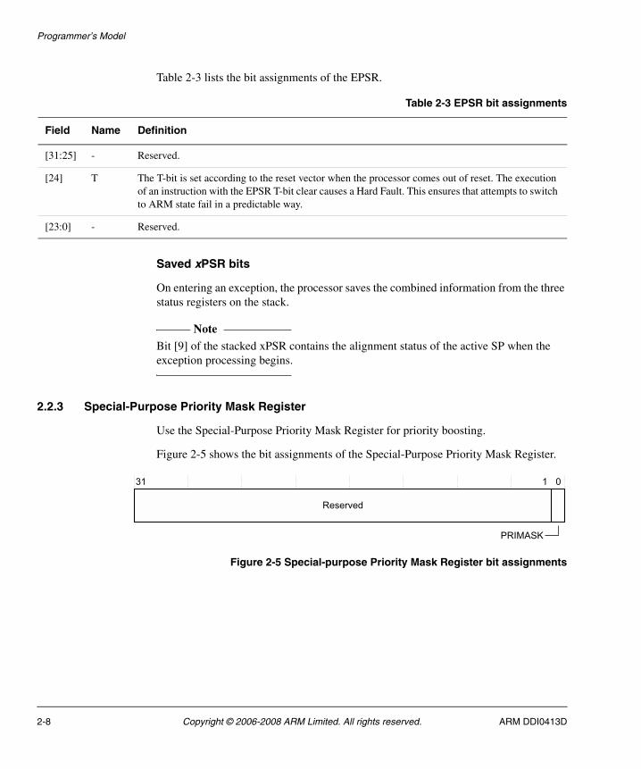
2.2.3 Special-Purpose Priority Mask Register
Use the Special-Purpose Priority Mask Register for priority boosting.
Figure 2-5 shows the bit assignments of the Special-Purpose Priority Mask Register.
Figure 2-5 Special-purpose Priority Mask Register bit assignments
Table 2-3 EPSR bit assignments
Field Name Definition
[31:25] - Reserved.
[24] T The T-bit is set according to the reset vector when the processor comes out of reset. The execution of an instruction with the EPSR T-bit clear causes a Hard Fault. This ensures that attempts to switch to ARM state fail in a predictable way.
[23:0] - Reserved.
31 1 0
Reserved
PRIMASK
2-8 Copyright © 2006-2008 ARM Limited. All rights reserved. ARM DDI0413D

Programmer’s Model
Table 2-4 lists the bit assignments of the Special-Purpose Priority Mask Register.
You can access the Special-Purpose Priority Mask Register using the MSR and MRS instructions. You can also use the CPS instruction to set or clear PRIMASK.
2.2.4 Special-Purpose Control Register
The Special-Purpose Control Register identifies the stack pointers used.
Figure 2-6 shows the bit assignments of the Special-purpose Control Register.
Figure 2-6 Special-Purpose Control Register bit assignments
Table 2-5 lists bit assignments of the Special-Purpose Control Register.
For writes from Handler mode occurring as part of an exception return, see the ARMv6-M Architecture Reference Manual.
Table 2-4 Special-Purpose Priority Mask Register bit assignments
Field Name Function
[31:1] - Reserved
[0] PRIMASK When set, raises execution priority to 0
31 2 1 0
Reserved
Active stack pointerReserved
Table 2-5 Special-Purpose Control Register bit assignments
Field Name Function
[31:2] - Reserved
[1] Active stack pointer
Defines the stack to use:
0 = SP_main is used for the current stack
1 = For Thread mode, SP_process is used for the current stacka.
a. Attempts to set this bit from Handler mode are ignored.
[0] - Reserved
ARM DDI0413D Copyright © 2006-2008 ARM Limited. All rights reserved. 2-9

Programmer’s Model
2.3 Data types
The processor supports the following data types:
• 32-bit words
• 16-bit halfwords
• 8-bit bytes.
Note Unless otherwise stated the core can access all regions of the memory map, including the code region, with all data types. To support this, the system, including memories, must support subword writes without corrupting neighboring bytes in that word.
2-10 Copyright © 2006-2008 ARM Limited. All rights reserved. ARM DDI0413D

Programmer’s Model
2.4 Memory formats
The processor views memory as a linear collection of bytes numbered in ascending order:
• The word at address A consists of the bytes at address A,A+1,A+2,A+3
• The halfword at address A consists of the bytes at address A,A+1
• The halfword at address A+2 consists of the bytes at address A+2,A+3
• The word at address A therefore consists of the halfwords at address A,A+2.
Table 2-6 shows the required mapping for an AHB-Lite interface. Table 2-6 also shows how the slaves use the HSIZE and the HADDR signals to determine which byte lanes are active on the data buses HWDATA and HRDATA.
On the TCM interface, the byte write enables are to be used for writes to ensure the correct byte lanes on the write data bus are written. All TCM reads are performed as word accesses and the processor will select the appropriate byte lanes depending on the requested access size and the address alignment.
Note These properties are endian-independent.
Endianness affects the numeric significance given to the bytes within the word or halfword, by the master performing the access. For a little-endian access, the byte with the highest address within the word or halfword has the highest numerical significance. For a big-endian access, the byte with the lowest address has the highest numerical significance.
For more details on endianness, see the ARMv6-M Architecture Reference Manual.
Table 2-6 Required mapping for an AHB-Lite interface
HSIZE HADDR[1:0] DATA[31:24] DATA[23:16] DATA[15:8] DATA[7:0]
Word 0 x x x x
Halfword 0 - - x x
Halfword 2 x x - -
Byte 0 - - - x
Byte 1 - - x -
Byte 2 - x - -
Byte 3 x - - -
ARM DDI0413D Copyright © 2006-2008 ARM Limited. All rights reserved. 2-11

Programmer’s Model
Accesses to the PPB space are always in little-endian format. The processor correctly interprets PPB data even when configured for big-endian operation.
2-12 Copyright © 2006-2008 ARM Limited. All rights reserved. ARM DDI0413D

Programmer’s Model
2.5 Instruction set
The processor supports all ARMv6-M Thumb and Thumb-2 instructions. For information on ARMv6-M Thumb instructions, see the ARMv6-M Architecture Reference Manual. The processor does not support ARM instructions.
ARM DDI0413D Copyright © 2006-2008 ARM Limited. All rights reserved. 2-13

Programmer’s Model
2-14 Copyright © 2006-2008 ARM Limited. All rights reserved. ARM DDI0413D
Chapter 3 Memory Map
This chapter describes the processor fixed memory map. It contains the following section:
• About the memory map on page 3-2.
ARM DDI0413D Copyright © 2006-2008 ARM Limited. All rights reserved. 3-1

Memory Map
3.1 About the memory map
Figure 3-1 shows the fixed memory map.
Figure 3-1 Processor memory map
DTCM
SRAM
Reserved0xE0000000
DW
BP
Reserved
Reserved
Reserved
0xE0001000
NVIC
Reserved
0x00000000
Reserved
Code
0x1FFFFFFF
SRAM
0x20000000
0x3FFFFFFF0x40000000
0.5GB
0.5GB
1GB
0xDFFFFFFF
Reserved
0xE0000000
0xE0100000
0xFFFFFFFF
0xE0002000
0xE0003000
0xE000E000
0xE000F000
0xE0041000
1MB ITCM (Lower Alias)0x00000000
0x00100000
0x1FFFFFFF
0xE0040000
0xE0042000
private peripheral bus
0xE00FFFFFROM Table
0xE00FF000
0x200000000x20100000
0x3FFFFFFF
1MB
External device
Peripheral 0.5GB
1GB
0x9FFFFFFF0xA0000000
0x5FFFFFFF0x60000000
Debug control0xE000ED00
External511MB
External0x0FFFFFFF
External
ITCM (Upper Alias)0x100000000x1000FFFF0x10010000
3-2 Copyright © 2006-2008 ARM Limited. All rights reserved. ARM DDI0413D
Memory Map
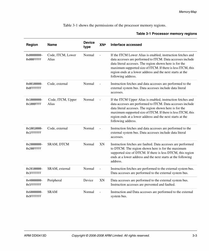
Table 3-1 shows the permissions of the processor memory regions.
Table 3-1 Processor memory regions
Region NameDevice type XNa Interface accessed
0x00000000- 0x000FFFFF
Code, ITCM, Lower Alias
Normal - If the ITCM Lower Alias is enabled, instruction fetches and data accesses are performed to ITCM. Data accesses include data literal accesses. The region shown here is for the maximum supported size of ITCM. If there is less ITCM, this region ends at a lower address and the next starts at the following address.
0x00100000- 0x0FFFFFFF
Code, external Normal - Instruction fetches and data accesses are performed to the external system bus. Data accesses include data literal accesses.
0x10000000- 0x1000FFFF
Code, ITCM, Upper Alias
Normal - If the ITCM Upper Alias is enabled, instruction fetches and data accesses are performed to ITCM. Data accesses include data literal accesses. The region shown here is for the maximum supported size of ITCM. If there is less ITCM, this region ends at a lower address and the next starts at the following address.
0x10010000- 0x1FFFFFFF
Code, external Normal - Instruction fetches and data accesses are performed to the external system bus. Data accesses include data literal accesses.
0x20000000- 0x200FFFFF
SRAM, DTCM Normal XN Instruction fetches are faulted. Data accesses are performed to DTCM. The region shown here is for the maximum supported size of DTCM. If there is less DTCM, this region ends at a lower address and the next starts at the following address.
0x20100000- 0x3FFFFFFF
SRAM, external Normal - Instruction fetches are performed to the external system bus. Data accesses are performed to the external system bus.
0x40000000- 0x5FFFFFFF
Peripheral Device XN Data accesses are performed to the external system bus. Instruction accesses are prevented and faulted.
0x60000000- 0x9FFFFFFF
SRAM Normal - Instruction and Data accesses are performed to the external system bus.
ARM DDI0413D Copyright © 2006-2008 ARM Limited. All rights reserved. 3-3
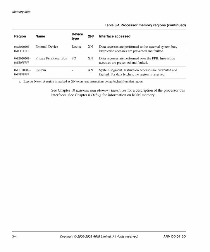
Memory Map
See Chapter 10 External and Memory Interfaces for a description of the processor bus interfaces. See Chapter 8 Debug for information on ROM memory.
0xA0000000- 0xDFFFFFFF
External Device Device XN Data accesses are performed to the external system bus. Instruction accesses are prevented and faulted.
0xE0000000- 0xE00FFFFF
Private Peripheral Bus SO XN Data accesses are performed over the PPB. Instruction accesses are prevented and faulted.
0xE0100000- 0xFFFFFFFF
System - XN System segment. Instruction accesses are prevented and faulted. For data fetches, the region is reserved.
a. Execute Never. A region is marked as XN to prevent instructions being fetched from that region.
Table 3-1 Processor memory regions (continued)
Region NameDevice type XNa Interface accessed
3-4 Copyright © 2006-2008 ARM Limited. All rights reserved. ARM DDI0413D
Chapter 4 Exceptions
This chapter describes the exception model of the processor. It contains the following sections:
• About the exception model on page 4-2
• Exception types on page 4-3
• Exception priority on page 4-5
• Stacks on page 4-7
• Pre-emption on page 4-8
• Exception exit on page 4-10
• Late-arrival on page 4-12
• Exception control transfer on page 4-13
• Activation levels on page 4-14
• Lock-up on page 4-16.
ARM DDI0413D Copyright © 2006-2008 ARM Limited. All rights reserved. 4-1

Exceptions
4.1 About the exception model
The processor and the Nested Vectored Interrupt Controller (NVIC) prioritize and handle all exceptions. All exceptions are handled in Handler mode. Processor state is automatically stored to the stack on an exception and automatically restored from the stack at the end of the exception handler. The following features enable efficient, low latency exception handling:
• Automatic state saving and restoring. The processor pushes state registers on the stack when entering the exception and pops them when exiting the exception with no instruction overhead.
For information on what content is stacked, see Pre-emption on page 4-8.
• Automatic reading of the vector table entry that contains the exception handler address.
Note Vector table entries are ARM or Thumb interworking compatible values.
Bit[0] of the vector value is loaded into the EPSR T-bit on exception entry. Creating a table entry with bit [0] clear generates a Hard Fault on the first instruction of the handler corresponding to this vector.
• Closely-coupled interface between the processor and the NVIC to enable efficient processing of interrupts and processing of late-arriving interrupts with higher priority.
• Configurable number of interrupts, from 1, 8, 16, or 32.
• Two bits of configurable interrupt priority providing four levels.
• Separate stacks for Handler and Thread modes if the Operating System (OS) extension is implemented.
• Exception control transfer using the calling conventions of the C/C++ standard ARM Architecture Procedure Call Standard (AAPCS). For more information, see the Application Binary Interface for the ARM Architecture (The Base Standard).
• Priority masking to support critical regions.
Note The number of interrupts are configured during implementation. Software can choose to enable a subset of the configured number of hardware interrupts.
4-2 Copyright © 2006-2008 ARM Limited. All rights reserved. ARM DDI0413D

Exceptions
4.2 Exception types
Various types of exceptions exist in the processor. A fault is an exception that results from an error condition. Faults can be reported synchronously or asynchronously with respect to the instruction that caused them. In general, faults are reported synchronously. Faults caused by writes over the external AHB bus are asynchronous faults. A synchronous fault is always reported with the instruction that caused the fault. An asynchronous fault does not guarantee how it is reported with respect to the instruction that caused the fault.
For more information on exceptions, see the ARMv6-M Architecture Reference Manual.
Table 4-1 shows the exception type, position, and priority. Position refers to the word offset of the exception vectors from the start of the vector table, which is always at address 0x0. The lower numbers shown in the Priority column of the table are higher priority. How the types are activated, synchronously or asynchronously, is also shown. The exact meaning and use of priorities is explained in Exception priority on page 4-5.
Table 4-1 Exception types
Position Exception type Priority Description Activated
- - - Stack top is loaded from first entry of vector table on reset.
-
1 Reset –3 (highest) Invoked on power up and warm reset. On first instruction, drops to lowest priority, Thread mode.
Asynchronous
2 Non-maskable Interrupt
–2 This exception type cannot be:
• masked or prevented from activation by any other exception
• pre-empted by any other exception other than Reset.
Asynchronous
3 Hard Fault –1 All classes of Fault. Synchronous or asynchronous
4-10 - - Reserved. -
11 SVC Configurable System service call using the SVC instruction. Synchronous
12-13 - - Reserved. -
ARM DDI0413D Copyright © 2006-2008 ARM Limited. All rights reserved. 4-3
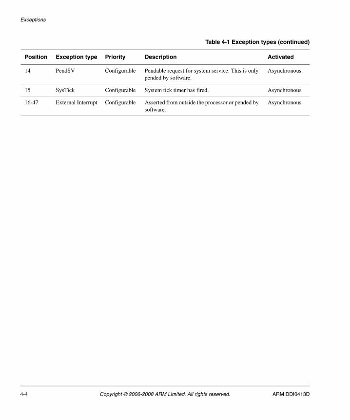
Exceptions
14 PendSV Configurable Pendable request for system service. This is only pended by software.
Asynchronous
15 SysTick Configurable System tick timer has fired. Asynchronous
16-47 External Interrupt Configurable Asserted from outside the processor or pended by software.
Asynchronous
Table 4-1 Exception types (continued)
Position Exception type Priority Description Activated
4-4 Copyright © 2006-2008 ARM Limited. All rights reserved. ARM DDI0413D

Exceptions
4.3 Exception priority
Table 4-2 shows how priority affects when and how the processor takes an exception. It lists the actions an exception can take based on priority.
In the processor exception model, priority determines when and how the processor takes exceptions. You can assign priority levels to interrupts.
4.3.1 Priority levels
The NVIC supports software-assigned priority levels. You can assign a priority level from 0 to 3 to an interrupt by writing to the two-bit IP_N field in an Interrupt Priority Register, see Interrupt Priority Registers on page 7-7. Priority level 0 is the highest priority level and priority level 3 is the lowest. For example, if you assign priority level 1 to IRQ[0] and priority level 0 to IRQ[31], then IRQ[31] has priority over IRQ[0].
Table 4-2 Exception scenarios
Scenario Description
Pre-emption A pended exception can interrupt the current execution thread if the priority of the pended exception is higher than the current execution priority.
When one exception pre-empts another, the exceptions are nested.
On exception entry the processor automatically saves processor state, which is pushed on to the stack. The vector corresponding to the exception is fetched. Execution begins at the address pointed to by the vector table value. Execution of the first instruction of the exception starts when the processor state has been saved. The state saving is performed over the ITCM, DTCM, or external AHB-Lite interface depending on:
• the value of the stack pointer when the processor registered the exception
• the size of the TCMs implemented.
The vector fetch is performed over the external AHB-Lite interface or the ITCM memory interface depending on the configuration of ITCM size.
Return When a valid return instruction is executed, the processor pops the stack and returns to a stacked exception or Thread mode.
On completion of an exception handler the processor automatically restores the processor state by popping the stack to restore the state prior to the exception.
Late-arriving A mechanism used by the processor to speed up pre-emption. If a higher priority exception arrives during state saving for a previous pre-emption, the processor switches to handling the higher priority exception instead and initiates the vector fetch for that exception. The state saving is not affected by late arrival, because the state that is saved is the same for both exceptions and the state saving continues uninterrupted. Late arriving exceptions are recognized up to the point where the vector fetch has been initiated. If a high priority exception is recognized too late to be handled as a late arrival, it is pended and subsequently pre-empts the original exception handler.
ARM DDI0413D Copyright © 2006-2008 ARM Limited. All rights reserved. 4-5

Exceptions
Note Software prioritization does not affect reset, Non-Maskable Interrupt (NMI), and Hard Fault. They always have higher priority than the external interrupts.
When multiple exceptions have the same priority number, the pending exception with the lowest exception number takes precedence. For example, if both IRQ[0] and IRQ[1] are priority level 1, then IRQ[0] has precedence over IRQ[1].
An exception is pre-empted if the handler receives an exception that has a higher priority. If the handler receives an interrupt of the same priority the exception is not pre-empted, irrespective of the interrupt number.
For more information on the IP_N fields, see Interrupt Priority Registers on page 7-7.
4-6 Copyright © 2006-2008 ARM Limited. All rights reserved. ARM DDI0413D
Exceptions
4.4 Stacks
The processor supports two separate stacks:
Process stack
You can configure Thread mode to use either SP_process or SP_main for its Stack Pointer (SP).
Note This is only available if the OS extension option is implemented. Contact
your implementation team for information.
Main stack Handler mode uses the main stack. SP_main is the SP register for the main stack. Thread mode uses SP_main out of reset.
Only one Stack Pointer register, SP_process or SP_main, is visible at any time, using R13.
When a thread is pre-empted, its context is automatically saved onto the stack that was active at the time the exception was recognized.
If an exception pre-empts Thread mode, the context of the pre-empted thread can be stacked using SP_process or SP_main depending on the value of the CONTROL[1] bit.
If an exception pre-empts another exception handler running in Handler mode, the pre-empted context can only be stacked using SP_main because this is the only stack pointer that can be active in Handler mode.
On exception return, the EXC_RETURN value determines which stack is used for the unstacking of context. The EXC_RETURN value loaded into R14 during exception entry points to the same stack that was used to stack the context. If your exception handler code moves the stack, you must ensure that the EXC_RETURN value used for exception return is correctly updated.
All exception handlers must use SP_main for their local variables.
When the OS extension option is implemented:
• you can configure Thread mode to use the process stack
• exception handlers always use SP_main.
Note MSR and MRS instructions have visibility of both stack pointers.
ARM DDI0413D Copyright © 2006-2008 ARM Limited. All rights reserved. 4-7

Exceptions
4.5 Pre-emption
This section describes the behavior of the processor when it takes an exception.
When the processor takes an exception, it automatically pushes the following eight registers to the stack:
• xPSR
• ReturnAddress( )
• Link Register (LR)
• R12
• R3
• R2
• R1
• R0.
For information on how ReturnAddress() relates to instruction address, see the ARMv6-M Architecture Reference Manual.
The SP is decremented by eight words on the completion of the stack push. Figure 4-1 shows the contents of the stack after an exception pre-empts the current program flow.
Figure 4-1 Stack contents after a pre-emption
Note • Figure 4-1 shows the order on the stack.
• Doubleword alignment of the stack pointer is enforced when stacking commences. Bit [2] of the stack pointer is saved as bit [9] of the stacked xPSR.
After returning from the exception, the processor automatically pops the eight registers from the stack. The exception return value, EXC_RETURN, is automatically loaded into the LR on exception entry to enable exception handlers to be written as normal C/C++ functions without the requirement for a veneer. See the ARMv6-M Architecture Reference Manual for more information.
Old SP
SP
xPSRReturnAddress()
LRr12r3r2r1r0
<previous>
4-8 Copyright © 2006-2008 ARM Limited. All rights reserved. ARM DDI0413D
Exceptions
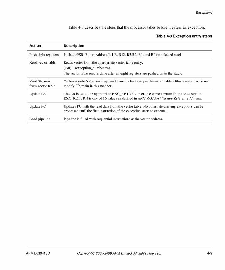
Table 4-3 describes the steps that the processor takes before it enters an exception.
Table 4-3 Exception entry steps
Action Description
Push eight registers Pushes xPSR, ReturnAddress(), LR, R12, R3,R2, R1, and R0 on selected stack.
Read vector table Reads vector from the appropriate vector table entry:
(0x0) + (exception_number *4).
The vector table read is done after all eight registers are pushed on to the stack.
Read SP_main from vector table
On Reset only, SP_main is updated from the first entry in the vector table. Other exceptions do not modify SP_main in this manner.
Update LR The LR is set to the appropriate EXC_RETURN to enable correct return from the exception. EXC_RETURN is one of 16 values as defined in ARMv6-M Architecture Reference Manual.
Update PC Updates PC with the read data from the vector table. No other late-arriving exceptions can be processed until the first instruction of the exception starts to execute.
Load pipeline Pipeline is filled with sequential instructions at the vector address.
ARM DDI0413D Copyright © 2006-2008 ARM Limited. All rights reserved. 4-9

Exceptions
4.6 Exception exit
The exception return instruction of a handler loads the PC with the EXC_RETURN value that was present in LR on entry to an exception handler. This indicates to the processor that the exception is complete and the processor initiates the exception exit sequence. See Returning the processor from an exception for the instructions that you can use to return from an exception.
When returning from an exception, the processor is either:
• returning to the last stacked exception
• returning to Thread mode if there are no stacked exceptions.
Table 4-4 describes the postamble sequence.
4.6.1 Returning the processor from an exception
Exception returns occur when one of the following instructions executed in Handler mode loads a value of 0xFXXXXXXX into the PC:
• POP that includes loading the PC
• BX with any register.
Table 4-4 Exception exit steps
Action Description
Select SP Sets CONTROL[1] based on EXC_RETURN.
Pop eight registers Pops R0, R1, R2, R3, R12, LR, PC, and xPSR from stack selected by EXC_RETURN.
The value of xPSR[5:0] loaded off the stack determines the exception number that defines the priority of the thread to be returned to.
The value of EXC_RETURN determines which mode is returned to.
4-10 Copyright © 2006-2008 ARM Limited. All rights reserved. ARM DDI0413D
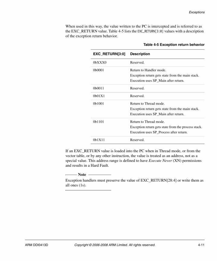
Exceptions
When used in this way, the value written to the PC is intercepted and is referred to as the EXC_RETURN value. Table 4-5 lists the EXC_RETURN[3:0] values with a description of the exception return behavior.
If an EXC_RETURN value is loaded into the PC when in Thread mode, or from the vector table, or by any other instruction, the value is treated as an address, not as a special value. This address range is defined to have Execute Never (XN) permissions and results in a Hard Fault.
Note Exception handlers must preserve the value of EXC_RETURN[28:4] or write them as all ones (1s).
Table 4-5 Exception return behavior
EXC_RETURN[3:0] Description
0bXXX0 Reserved.
0b0001 Return to Handler mode.
Exception return gets state from the main stack.
Execution uses SP_Main after return.
0b0011 Reserved.
0b01X1 Reserved.
0b1001 Return to Thread mode.
Exception return gets state from the main stack.
Execution uses SP_Main after return.
0b1101 Return to Thread mode.
Exception return gets state from the process stack.
Execution uses SP_Process after return.
0b1X11 Reserved.
ARM DDI0413D Copyright © 2006-2008 ARM Limited. All rights reserved. 4-11
Exceptions
4.7 Late-arrival
A late-arriving exception can be handled in preference to a previous exception if the vector fetch has not started and the late-arriving exception has:
• a higher priority than the previous exception
• the same priority but a lower exception number than the previous exception.
A late-arriving exception causes a change of vector address fetch and exception prefetch. State saving is not performed for the late-arriving exception because it has already been performed for the initial exception and so does not have to be repeated. In this case, execution commences at the vector of the late arriving exception while the previous exception remains pending.
If a high priority exception is recognized after the vector fetch of the original exception has started, the late-arriving exception cannot use the context already stacked for the original exception. In this case, the original exception handler is pre-empted and its context is saved onto the stack.
4-12 Copyright © 2006-2008 ARM Limited. All rights reserved. ARM DDI0413D
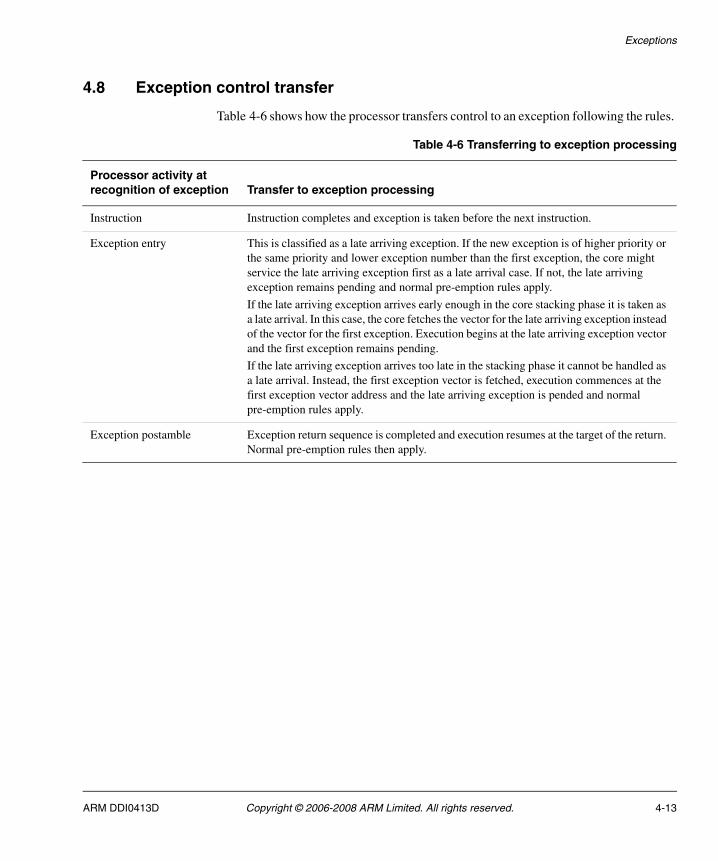
Exceptions
4.8 Exception control transfer
Table 4-6 shows how the processor transfers control to an exception following the rules.
Table 4-6 Transferring to exception processing
Processor activity at recognition of exception Transfer to exception processing
Instruction Instruction completes and exception is taken before the next instruction.
Exception entry This is classified as a late arriving exception. If the new exception is of higher priority or the same priority and lower exception number than the first exception, the core might service the late arriving exception first as a late arrival case. If not, the late arriving exception remains pending and normal pre-emption rules apply.
If the late arriving exception arrives early enough in the core stacking phase it is taken as a late arrival. In this case, the core fetches the vector for the late arriving exception instead of the vector for the first exception. Execution begins at the late arriving exception vector and the first exception remains pending.
If the late arriving exception arrives too late in the stacking phase it cannot be handled as a late arrival. Instead, the first exception vector is fetched, execution commences at the first exception vector address and the late arriving exception is pended and normal pre-emption rules apply.
Exception postamble Exception return sequence is completed and execution resumes at the target of the return. Normal pre-emption rules then apply.
ARM DDI0413D Copyright © 2006-2008 ARM Limited. All rights reserved. 4-13

Exceptions
4.9 Activation levels
When no exceptions are active, the processor is in Thread mode. When an exception or fault handler is active, the processor enters Handler mode. Table 4-7 lists the stacks and associated active exception and activation levels.
Table 4-8 lists the transition rules for all exception types and how they relate to the access rules and stack model.
Table 4-9 on page 4-15 lists exception subtype transitions.
Table 4-7 Stack activation levels
Active exception Activation level Stack
None Thread mode Main or process
Exception active Asynchronous pre-emption level Main
Fault handler active Asynchronous or Synchronous pre-emption level Main
Table 4-8 Exception transitions
Active exception Triggering event Transition type Stack
Reset Reset signal Thread Main
ISR or NMIa Set-pending software instruction or hardware signal Asynchronous pre-emption Main
Hard Fault Any fault Synchronous or asynchronous pre-emption
Main
SVCb SVC instruction Synchronous pre-emption Main
a. Nonmaskable interrupt.b. Supervisor Call.
4-14 Copyright © 2006-2008 ARM Limited. All rights reserved. ARM DDI0413D
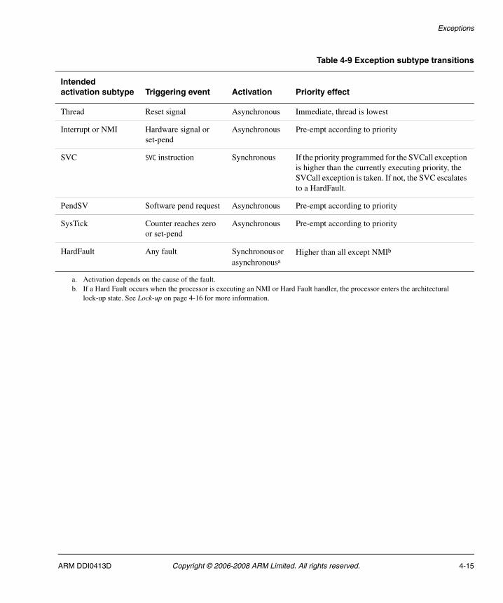
Exceptions
Table 4-9 Exception subtype transitions
Intended activation subtype Triggering event Activation Priority effect
Thread Reset signal Asynchronous Immediate, thread is lowest
Interrupt or NMI Hardware signal or set-pend
Asynchronous Pre-empt according to priority
SVC SVC instruction Synchronous If the priority programmed for the SVCall exception is higher than the currently executing priority, the SVCall exception is taken. If not, the SVC escalates to a HardFault.
PendSV Software pend request Asynchronous Pre-empt according to priority
SysTick Counter reaches zero or set-pend
Asynchronous Pre-empt according to priority
HardFault Any fault Synchronous or asynchronousa
Higher than all except NMIb
a. Activation depends on the cause of the fault.b. If a Hard Fault occurs when the processor is executing an NMI or Hard Fault handler, the processor enters the architectural
lock-up state. See Lock-up on page 4-16 for more information.
ARM DDI0413D Copyright © 2006-2008 ARM Limited. All rights reserved. 4-15

Exceptions
4.10 Lock-up
The processor has a lock-up state that is entered when an unrecoverable condition occurs. The cause of unrecoverable conditions are asynchronous or synchronous faults, including an escalated SVC instruction. For more information on unrecoverable conditions, see the ARMv6-M Architecture Reference Manual.
The processor can enter the lock-up state at a priority of -1 or -2. An NMI can be taken and cause the processor to leave the lock-up state if it was at a priority of -1.
A debugger can also cause the processor to exit the lock-up state.
The LOCKUP pin from the processor indicates the that the processor is in the lock-up state.
4-16 Copyright © 2006-2008 ARM Limited. All rights reserved. ARM DDI0413D
Chapter 5 Clocks and Resets
This chapter describes the processor clocking and resets. It contains the following section:
• About clocks and resets on page 5-2.
ARM DDI0413D Copyright © 2006-2008 ARM Limited. All rights reserved. 5-1
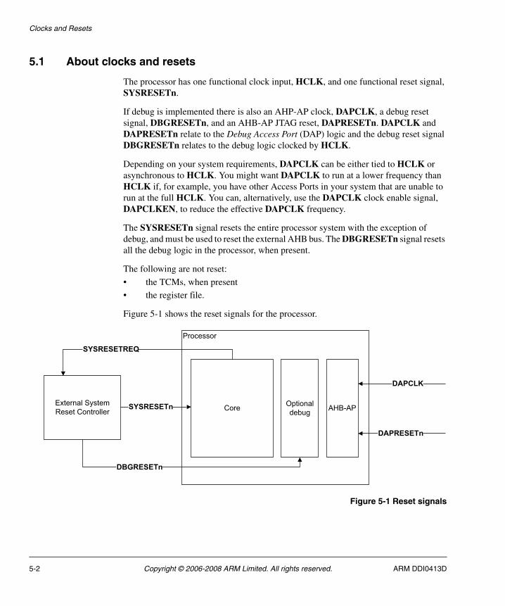
Clocks and Resets
5.1 About clocks and resets
The processor has one functional clock input, HCLK, and one functional reset signal, SYSRESETn.
If debug is implemented there is also an AHP-AP clock, DAPCLK, a debug reset signal, DBGRESETn, and an AHB-AP JTAG reset, DAPRESETn. DAPCLK and DAPRESETn relate to the Debug Access Port (DAP) logic and the debug reset signal DBGRESETn relates to the debug logic clocked by HCLK.
Depending on your system requirements, DAPCLK can be either tied to HCLK or asynchronous to HCLK. You might want DAPCLK to run at a lower frequency than HCLK if, for example, you have other Access Ports in your system that are unable to run at the full HCLK. You can, alternatively, use the DAPCLK clock enable signal, DAPCLKEN, to reduce the effective DAPCLK frequency.
The SYSRESETn signal resets the entire processor system with the exception of debug, and must be used to reset the external AHB bus. The DBGRESETn signal resets all the debug logic in the processor, when present.
The following are not reset:
• the TCMs, when present
• the register file.
Figure 5-1 shows the reset signals for the processor.
Figure 5-1 Reset signals
External System Reset Controller
Processor
SYSRESETn OptionaldebugCore
SYSRESETREQ
DBGRESETn
AHB-AP
DAPCLK
DAPRESETn
5-2 Copyright © 2006-2008 ARM Limited. All rights reserved. ARM DDI0413D
Clocks and Resets
Note Both DBGRESETn and SYSRESETn must be asserted at power on reset.
Depending on your requirements, you might want to reset the system outside the processor independent of the state of SYSRESETREQ. If this is the case, ensure that:
• Any logic required for debug is not reset.
• SYSRESETREQ is not connected combinatorially to SYSRESETn. SYSRESETREQ must be registered to ensure that SYSRESETn is driven for the minimum reset time of your FPGA. SYSRESETREQ is cleared by SYSRESETn.
• DBGRESETn is driven at power on reset and not by SYSRESETREQ otherwise the debugger cannot maintain a connection when the processor is reset.
• If DBGRESETn is driven SYSRESETn must also be driven.
Note If you do not reset the system at the same time as the processor, you must also ensure accesses that might be in progress as reset occurs do not disrupt the system.
You must ensure that SYSRESETn and DBGRESETn are:
• held LOW for a minimum of 3 cycles
• deasserted synchronously to HCLK.
You can stop all of the processor clocks indefinitely without loss of state.
Note • When the External AHB system and the processor are held in reset by
SYSRESETn, the debugger can only access the debug portion of the PPB space of the processor and the TCMs. The debugger cannot access external memory space.
• If SYSRESETn is asserted during a DAP access to the external AHB system or to the PPB space, except to debug registers, the results of the access cannot be guaranteed. For example, a read transaction might receive corrupt data and a faulting transaction might not be recognized by the DAP.
• You must ensure that DAPRESETn is held LOW for a minimum of two cycles and deasserted synchronously to DAPCLK.
ARM DDI0413D Copyright © 2006-2008 ARM Limited. All rights reserved. 5-3

Clocks and Resets
5-4 Copyright © 2006-2008 ARM Limited. All rights reserved. ARM DDI0413D
Chapter 6 System Control
This chapter describes the registers that program the processor. It contains the following sections:
• About system control on page 6-2
• System control register descriptions on page 6-4.
ARM DDI0413D Copyright © 2006-2008 ARM Limited. All rights reserved. 6-1
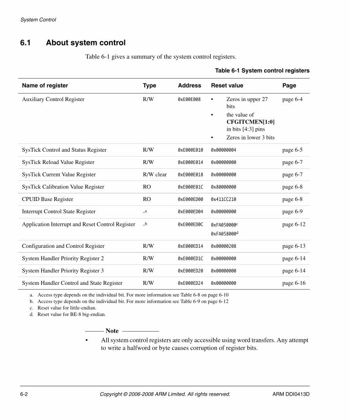
System Control
6.1 About system control
Table 6-1 gives a summary of the system control registers.
Note • All system control registers are only accessible using word transfers. Any attempt
to write a halfword or byte causes corruption of register bits.
Table 6-1 System control registers
Name of register Type Address Reset value Page
Auxiliary Control Register R/W 0xE00E008 • Zeros in upper 27 bits
• the value of CFGITCMEN[1:0] in bits [4:3] pins
• Zeros in lower 3 bits
page 6-4
SysTick Control and Status Register R/W 0xE000E010 0x00000004 page 6-5
SysTick Reload Value Register R/W 0xE000E014 0x00000000 page 6-7
SysTick Current Value Register R/W clear 0xE000E018 0x00000000 page 6-7
SysTick Calibration Value Register RO 0xE000E01C 0x80000000 page 6-8
CPUID Base Register RO 0xE000ED00 0x411CC210 page 6-8
Interrupt Control State Register -a 0xE000ED04 0x00000000 page 6-9
Application Interrupt and Reset Control Register -b 0xE000ED0C 0xFA050000c
0xFA058000d
page 6-12
Configuration and Control Register R/W 0xE000ED14 0x00000208 page 6-13
System Handler Priority Register 2 R/W 0xE000ED1C 0x00000000 page 6-14
System Handler Priority Register 3 R/W 0xE000ED20 0x00000000 page 6-14
System Handler Control and State Register R/W 0xE000ED24 0x00000000 page 6-16
a. Access type depends on the individual bit. For more information see Table 6-8 on page 6-10b. Access type depends on the individual bit. For more information see Table 6-9 on page 6-12c. Reset value for little-endian.d. Reset value for BE-8 big-endian.
6-2 Copyright © 2006-2008 ARM Limited. All rights reserved. ARM DDI0413D

System Control
• If you do not have OS extension implemented the addresses 0xE000E010, 0xE000E014, 0xE000E018, and 0xE000E01C are reserved.
ARM DDI0413D Copyright © 2006-2008 ARM Limited. All rights reserved. 6-3
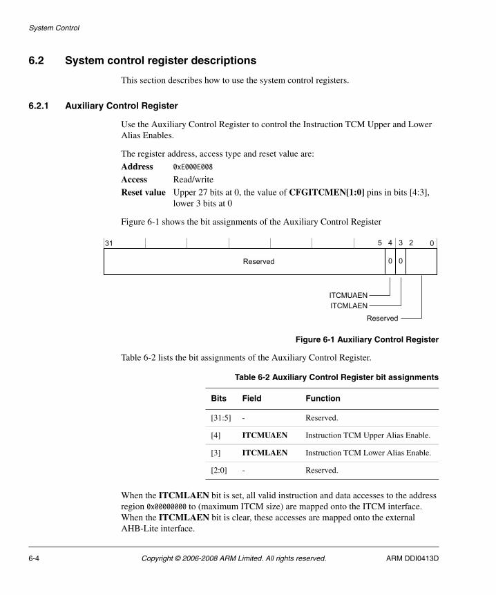
System Control
6.2 System control register descriptions
This section describes how to use the system control registers.
6.2.1 Auxiliary Control Register
Use the Auxiliary Control Register to control the Instruction TCM Upper and Lower Alias Enables.
The register address, access type and reset value are:
Address 0xE000E008
Access Read/write
Reset value Upper 27 bits at 0, the value of CFGITCMEN[1:0] pins in bits [4:3], lower 3 bits at 0
Figure 6-1 shows the bit assignments of the Auxiliary Control Register
Figure 6-1 Auxiliary Control Register
Table 6-2 lists the bit assignments of the Auxiliary Control Register.
When the ITCMLAEN bit is set, all valid instruction and data accesses to the address region 0x00000000 to (maximum ITCM size) are mapped onto the ITCM interface. When the ITCMLAEN bit is clear, these accesses are mapped onto the external AHB-Lite interface.
Reserved
31 0
ITCMUAENITCMLAEN
00
2345
Reserved
Table 6-2 Auxiliary Control Register bit assignments
Bits Field Function
[31:5] - Reserved.
[4] ITCMUAEN Instruction TCM Upper Alias Enable.
[3] ITCMLAEN Instruction TCM Lower Alias Enable.
[2:0] - Reserved.
6-4 Copyright © 2006-2008 ARM Limited. All rights reserved. ARM DDI0413D
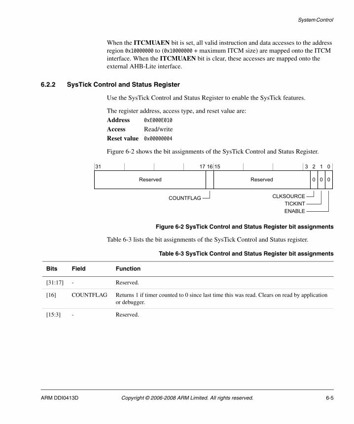
System Control
When the ITCMUAEN bit is set, all valid instruction and data accesses to the address region 0x10000000 to (0x10000000 + maximum ITCM size) are mapped onto the ITCM interface. When the ITCMUAEN bit is clear, these accesses are mapped onto the external AHB-Lite interface.
6.2.2 SysTick Control and Status Register
Use the SysTick Control and Status Register to enable the SysTick features.
The register address, access type, and reset value are:
Address 0xE000E010
Access Read/write
Reset value 0x00000004
Figure 6-2 shows the bit assignments of the SysTick Control and Status Register.
Figure 6-2 SysTick Control and Status Register bit assignments
Table 6-3 lists the bit assignments of the SysTick Control and Status register.
0Reserved
31 17 16 15 3 2 1 0
Reserved 0 0
COUNTFLAG CLKSOURCETICKINTENABLE
Table 6-3 SysTick Control and Status Register bit assignments
Bits Field Function
[31:17] - Reserved.
[16] COUNTFLAG Returns 1 if timer counted to 0 since last time this was read. Clears on read by application or debugger.
[15:3] - Reserved.
ARM DDI0413D Copyright © 2006-2008 ARM Limited. All rights reserved. 6-5
System Control
6.2.3 SysTick Reload Value Register
Use the SysTick Reload Value Register to specify the start value to load into the SysTick Current Value Register when the counter reaches 0. It can be any value in range 0x00000001-0x00FFFFFF. A start value of 0 is possible, but has no effect because the SysTick interrupt and COUNTFLAG are activated when counting from 1 to 0.
The RELOAD value can be calculated according to its use. For example:
• A multi-shot timer has a SysTick interrupt RELOAD of N-1 to generate a timer period of N processor clock cycles. For example, if the SysTick interrupt is required every 100 clock pulses, 99 must be written into RELOAD.
• A single shot timer has a SysTick interrupt RELOAD of N to deliver a single SysTick interrupt after a delay of N processor clock cycles. For example, if a SysTick interrupt is next required after 400 clock pulses, you must write 400 into RELOAD.
The register address, access type, and reset value are:
Address 0xE000E014
Access Read/write
Reset value 0x00000000
Figure 6-3 on page 6-7 shows the bit assignments of the SysTick Reload Value Register.
[2] CLKSOURCE Always reads as one:
1 = processor clock.
Indicates that SysTick uses the processor clock, HCLK.
[1] TICKINT 1 = counting down to zero pends the SysTick handler.
0 = counting down to zero does not pend the SysTick handler. Software can use COUNTFLAG to determine if the SysTick handler has ever counted to zero.
[0] ENABLE 1 = counter operates in a multi-shot way. That is, counter loads with the Reload value and then begins counting down. On reaching 0, it sets the COUNTFLAG to 1 and optionally pends the SysTick handler, based on TICKINT. It then loads the Reload value again and begins counting.
0 = counter disabled.
Table 6-3 SysTick Control and Status Register bit assignments (continued)
Bits Field Function
6-6 Copyright © 2006-2008 ARM Limited. All rights reserved. ARM DDI0413D

System Control
Figure 6-3 SysTick Reload Value Register bit assignments
Table 6-4 lists the bit assignments of the SysTick Reload Value Register.
6.2.4 SysTick Current Value Register
Use the SysTick Current Value Register to find the current value in the register.
The register address, access type, and reset value are:
Address 0xE000E018
Access Read/write clear
Reset value 0x00000000
Figure 6-4 shows the bit assignments of the SysTick Current Value Register.
Figure 6-4 SysTick Current Value Register bit assignments
Table 6-5 lists the bit assignments of the SysTick Current Value Register.
31 0
RELOADReserved
2324
Table 6-4 SysTick Reload Value Register bit assignments
Bits Field Function
[31:24] - Reserved
[23:0] RELOAD Value to load into the SysTick Current Value Register when the counter reaches 0
31 0
CURRENTReserved
2324
Table 6-5 SysTick Current Value Register bit assignments
Bits Field Function
[31:24] - Reserved.
[23:0] CURRENT Reads return the current value of the SysTick counter.
This register is write-clear. Writing to it with any value clears the register to 0. Clearing this register also clears the COUNTFLAG bit of the SysTick Control and Status Register.
ARM DDI0413D Copyright © 2006-2008 ARM Limited. All rights reserved. 6-7

System Control
6.2.5 SysTick Calibration Value Register
Use the SysTick Calibration Value Register to enable software to scale to any required speed using divide and multiply.
The register address, access type, and reset value are:
Address 0xE000E01C
Access Read-only
Reset value 0x80000000
Figure 6-5 shows the bit assignments of the SysTick Calibration Value Register.
Figure 6-5 SysTick Calibration Value Register bit assignments
Table 6-6 lists the bit assignments of the SysTick Calibration Value Register.
6.2.6 CPU ID Base Register
Read the CPU ID Base Register to determine:
• the ID number of the processor core
• the version number of the processor core
• the implementation details of the processor core.
The register address, access type, and reset value are:
Address 0xE000ED00
Access Read-only
31 0
TENMSReserved
232430
SKEWNOREF
29
Table 6-6 SysTick Calibration Value Register bit assignments
Bits Field Function
[31] NOREF Reads as one. Indicates that no separate reference clock is provided.
[30] SKEW Reads as zero. Calibration value for the 10ms inexact timing is not known because TENMS is not known. This can affect its suitability as a software real time clock.
[29:24] - Reserved.
[23:0] TENMS Reads as zero. Indicates calibration value is not known.
6-8 Copyright © 2006-2008 ARM Limited. All rights reserved. ARM DDI0413D

System Control
Reset value 0x410CC210
Figure 6-6 shows the bit assignments of the CPUID Base Register.
Figure 6-6 CPUID Base Register bit assignments
Table 6-7 lists the bit assignments of the CPUID Base Register.
6.2.7 Interrupt Control State Register
Use the Interrupt Control State Register to:
• set a pending Non-Maskable Interrupt (NMI)
• set or clear a pending PendSV
• set or clear a pending SysTick
• check for pending exceptions
• check the vector number of the highest priority pended exception
• check the vector number of the active exception.
The register address, access type, and reset value are:
Address 0xE000ED04.
31 16 15 4 3 0
IMPLEMENTER REVISIONPARTNO
24 23 20 19
VARIANT Constant
Table 6-7 CPUID Base Register bit assignments
Bits Field Function
[31:24] IMPLEMENTER Implementor code:
0x41 = ARM
[23:20] VARIANT Implementation defined variant number:
0x0 for r0p0 and r0p1
0x1 for r1p0.
[19:16] Constant Reads as 0xC
[15:4] PARTNO Number of processor within family:
0xC21
[3:0] REVISION Implementation defined revision number:
0x0 = r0p0, r1p0
0x1 = r0p1
ARM DDI0413D Copyright © 2006-2008 ARM Limited. All rights reserved. 6-9

System Control
Access Access type depends on the individual bit. For more information see Table 6-8.
Reset value 0x00000000.
Figure 6-7 shows the bit assignments of the Interrupt Control State Register.
Figure 6-7 Interrupt Control State Register bit assignments
Table 6-8 lists the bit assignments of the Interrupt Control State Register.
31 28 22 21 0
VECTACTIVE
30 29 27 26 2324 12 11
VECTPENDING
NMIPENDSET
PENDSVSETPENDSVCLR
ISRPREEMPTISRPENDING
Reserved
25
PENDSTSETPENDSTCLRReserved
Reserved
5618 17
Reserved
Table 6-8 Interrupt Control State Register bit assignments
Bits Field Type Function
[31] NMIPENDSET R/W On writes:
1 = set pending NMI
0 = no effect.
NMIPENDSET pends and activates an NMI. Because NMI is the highest-priority interrupt, it takes effect as soon as it registers unless the processor is at a priority of -2.
On reads, this bit returns the pending state of NMI.
[30:29] - - Reserved.
[28] PENDSVSETa R/W On writes:
1 = set pending PendSV
0 = no effect.
On reads this bit returns the pending state of PendSV.
6-10 Copyright © 2006-2008 ARM Limited. All rights reserved. ARM DDI0413D

System Control
[27] PENDSVCLRa WO On writes:
1 = clear pending PendSV
0 = no effect.
[26] PENDSTSETa R/W On writes:
1 = set pending SysTick
0 = no effect.
On reads this bit returns the pending state of SysTick.
[25] PENDSTCLRa WO On writes:
1 = clear pending SysTick
0 = no effect.
[24] - - Reserved.
[23] ISRPREEMPTb RO You must only use this at debug time. It indicates that a pending interrupt becomes active in the next running cycle. If C_MASKINTS is clear in the Debug Halting Control and Status Register, the interrupt is serviced:
1 = a pending exception is serviced on exit from the debug halt state
0 = a pending exception is not serviced.
[22] ISRPENDINGb RO External interrupt pending flag, where:
1 = interrupt pending
0 = interrupt not pending.
[21:18] - - Reserved.
[17:12] VECTPENDINGa RO Indicates the exception number for the highest priority pending exception:
0 = no pending exceptions
Non zero = The pending state includes the effect of memory-mapped enable and mask registers. It does not include the PRIMASK special-purpose register qualifier.
[11:6] - - Reserved.
[5:0] VECTACTIVEc RO Active exception number field:
0 = Thread mode
Non zero = the exception numberc of the currently active exception.
Reset clears the VECTACTIVE field.
a. OS Extension only, otherwise Reserved.b. Debug Extension only, otherwise it is Reserved.c. This is the same value as IPSR bits [5:0].
Table 6-8 Interrupt Control State Register bit assignments (continued)
Bits Field Type Function
ARM DDI0413D Copyright © 2006-2008 ARM Limited. All rights reserved. 6-11
System Control
6.2.8 Application Interrupt and Reset Control Register
Use the Application Interrupt and Reset Control Register to:
• determine data endianness
• clear all active state information from debug halt mode
• request a system reset.
The register address, access type, and reset value are:
Address 0xE000ED0C.
Access Access type depends on the individual bit. For more information see Table 6-9.
Reset value 0xFA050000 is the reset value for little-endian.
0xFA058000 is the reset value for BE-8 big-endian.
Figure 6-8 shows the bit assignments of the Application Interrupt and Reset Control Register.
Figure 6-8 Application Interrupt and Reset Control Register bit assignments
Table 6-9 lists the bit assignments of the Application Interrupt and Reset Control Register.
31 16 15 0
VECTKEY
12
Reserved
14
ENDIANNESS
3
SYSRESETREQReserved
Table 6-9 Application Interrupt and Reset Control Register bit assignments
Bits Field Type Function
[31:16] VECTKEY WO Register key. To write to other parts of this register, you must ensure 0x5FA is written into the VECTKEY field.
[15] ENDIANNESS RO Data endianness bit. The read value depends on the endian configuration implemented:
0 = little-endian
1 = BE-8 big-endian.
[14:3] - - Reserved.
6-12 Copyright © 2006-2008 ARM Limited. All rights reserved. ARM DDI0413D

System Control
6.2.9 Configuration and Control Register
The Configuration and Control Register permanently enables stack alignment and causes unaligned accesses to result in a Hard Fault.
The register address, access type, and reset value are:
Address 0xE000ED14
Access Read-only
Reset value 0x00000208
Figure 6-9 shows the bit assignments of the Configuration and Control Register.
Figure 6-9 Configuration and Control Register bit assignments
[2] SYSRESETREQ WO Writing 1 to this bit causes the SYSRESETREQ signal to the outer system to be asserted to request a reset. The intention is to force a large system reset of all major components except for debug. The C_HALT bit in the DHCSR is cleared as a result of the system reset requested. The debugger does not lose contact with the device.
[1] VECTCLRACTIVE WO Clears all active state information for fixed and configurable exceptions.
This bit:
• is self-clearing
• can only be set by the DAP when the processor is halted.
When this bit is set:
• clears all active exception status of the processor
• forces a return to Thread mode
• forces an IPSR of 0.
A debugger must re-initialize the stack.
[0] - - Reserved.
Table 6-9 Application Interrupt and Reset Control Register bit assignments (continued)
Bits Field Type Function
31 03 2
Reserved
ReservedUNALIGN_TRP
48
Reserved
9
STKALIGN
10
ARM DDI0413D Copyright © 2006-2008 ARM Limited. All rights reserved. 6-13

System Control
Table 6-10 lists the bit assignments of the Configuration and Control Register.
6.2.10 System handler priority registers
System handlers are a special class of exception handler that can have their priority set to any of the priority levels.
There are two system handler priority registers for prioritizing the following system handlers:
• SVCall, see System Handler Priority Register 2
• SysTick, see System Handler Priority Register 3 on page 6-15
• PendSV, see System Handler Priority Register 3 on page 6-15.
PendSV and SVCall are permanently enabled. You can enable or disable SysTick by writing to the SysTick Control and Status Register.
System Handler Priority Register 2
The register address, access type, and reset value are:
Address 0xE000ED1C
Access Read/write
Reset value 0x00000000
Figure 6-10 on page 6-15 shows the bit assignments of the System Handler Priority Register 2.
Table 6-10 Configuration and Control Register bit assignments
Bits Field Function
[31:10] - Reserved.
[9] STKALIGN Always set to 1. On exception entry, all exceptions are entered with 8-byte stack alignment and the context to restore it is saved. The SP is restored on the associated exception return.
[8:4] - Reserved.
[3] UNALIGN_TRP Indicates that all unaligned accesses results in a Hard Fault. Trap for unaligned access is fixed at 1.
[2:0] - Reserved.
6-14 Copyright © 2006-2008 ARM Limited. All rights reserved. ARM DDI0413D

System Control
Figure 6-10 System Handler Priority Register 2 bit assignments
Table 6-11 lists the bit assignments for the System Handler Priority Register 2.
System Handler Priority Register 3
The register address, access type, and reset value are:
Address 0xE000ED20
Access Read/write
Reset value 0x00000000
Figure 6-11 shows the bit assignments of the System Handler Priority Register 3.
Figure 6-11 System Handler Priority Register 3 bit assignments
31 30 29 0
PRI_11
Reserved
Table 6-11 System Handler Priority Register 2 bit assignments
Bits Field Function
[31:30] PRI_11 Priority of system handler 11, SVCall
[29:0] - Reserved
Reserved Reserved
PRI_15 PRI_14
31 23 024 212230 29
ARM DDI0413D Copyright © 2006-2008 ARM Limited. All rights reserved. 6-15

System Control
Table 6-12 lists the bit assignments of the System Handler Priority Registers.
6.2.11 System Handler Control and State Register
Use the System Handler Control and State Register to read or write the pending status of SVCall.
The register address, access type, and reset value are:
Address 0xE000ED24
Access Read/write
Reset value 0x00000000
Figure 6-12 shows the bit assignments of the System Handler and State Control Register.
Figure 6-12 System Handler Control and State Register bit assignments
Table 6-12 System Handler Priority Register 3 bit assignments
Bits Field Function
[31:30] PRI_15 Priority of system handler 15, SysTick
[29:24] - Reserved
[23:22] PRI_14 Priority of system handler 14, PendSV
[21:0] - Reserved
31 0
SVCALLPENDED
141516
ReservedReserved
6-16 Copyright © 2006-2008 ARM Limited. All rights reserved. ARM DDI0413D

System Control
Table 6-13 lists the bit assignments of the System Handler Control Register.
Note This register is only accessible as part of debug and not through the processor memory map.
Table 6-13 System Handler Control and State Register bit assignments
Bits Field Function
[31:16] - Reserved.
[15] SVCALLPENDED Reads as 1 if SVCall is pended.
If written to:
1 = Set pending SVCall
0 = Clear pending SVCall
[14:0] - Reserved.
ARM DDI0413D Copyright © 2006-2008 ARM Limited. All rights reserved. 6-17

System Control
6-18 Copyright © 2006-2008 ARM Limited. All rights reserved. ARM DDI0413D

Chapter 7 Nested Vectored Interrupt Controller
This chapter describes the Nested Vectored Interrupt Controller (NVIC). It contains the following sections:
• About the NVIC on page 7-2
• NVIC programmer’s model on page 7-3
• Level versus pulse interrupts on page 7-9
• Resampling level interrupts on page 7-10
• Interrupts as general purpose input on page 7-11.
ARM DDI0413D Copyright © 2006-2008 ARM Limited. All rights reserved. 7-1

Nested Vectored Interrupt Controller
7.1 About the NVIC
The NVIC supports interrupts that can be re-prioritized. The NVIC and the core of the processor are closely coupled, which enables low latency interrupt processing and efficient processing of late arriving interrupts.
All NVIC registers are only accessible using word transfers. Any attempt to write a halfword or byte individually causes corruption of the register bits.
NVIC registers are always little-endian.
Processor accesses are correctly handled regardless of the endian configuration of the processor.
DAP accesses must be interpreted as little-endian.
Processor exception handling is described in Chapter 4 Exceptions.
7-2 Copyright © 2006-2008 ARM Limited. All rights reserved. ARM DDI0413D

Nested Vectored Interrupt Controller
7.2 NVIC programmer’s model
This section describes the NVIC registers. It contains the following:
• NVIC register map
• NVIC register descriptions.
7.2.1 NVIC register map
Table 7-1 gives a summary of the NVIC registers.
7.2.2 NVIC register descriptions
The sections that follow describe how to use the NVIC registers.
Interrupt Set-Enable Register
Use the Interrupt Set-Enable Register to:
• enable interrupts
• determine which interrupts are currently enabled.
Table 7-1 NVIC registers
Name of register Type Address Reset value Page
Interrupt Set Enable Register R/W 0XE000E100 0x00000000 page 7-3
Interrupt Clear Enable Register R/W 0XE000E180 0x00000000 page 7-4
Interrupt Set Pending Register R/W 0XE000E200 0x00000000 page 7-5
Interrupt Clear Pending Register R/W 0XE000E280 0x00000000 page 7-6
Priority 0 Register R/W 0XE000E400 0x00000000 page 7-7
Priority 1 Register R/W 0XE000E404 0x00000000 page 7-7
Priority 2 Register R/W 0XE000E408 0x00000000 page 7-7
Priority 3 Register R/W 0XE000E40C 0x00000000 page 7-7
Priority 4 Register R/W 0XE000E410 0x00000000 page 7-7
Priority 5 Register R/W 0XE000E414 0x00000000 page 7-7
Priority 6 Register R/W 0XE000E418 0x00000000 page 7-7
Priority 7 Register R/W 0XE000E41C 0x00000000 page 7-7
ARM DDI0413D Copyright © 2006-2008 ARM Limited. All rights reserved. 7-3

Nested Vectored Interrupt Controller
Each bit in the register corresponds to one of 32 interrupts. Setting a bit in the Interrupt Set-Enable Register enables the corresponding interrupt.
When the enable bit of a pending interrupt is set, the processor activates the interrupt based on its priority. When the enable bit is clear, asserting the interrupt signal pends the interrupt, but it is not possible to activate the interrupt, regardless of its priority. Therefore, a disabled interrupt can serve as a latched general-purpose bit. You can read it and clear it without invoking an interrupt.
Clear the enable state by writing a 1 to the corresponding bit in the Interrupt Clear-Enable Register (see Interrupt Clear-Enable Register). This also clears the corresponding bit in the Interrupt Set-Enable Register (see Interrupt Set-Enable Register on page 7-3).
The register address, access type, and reset value are:
Address 0xE000E100
Access Read/write
Reset value 0x00000000
Table 7-2 lists the bit assignments of the Interrupt Set-Enable Register.
Interrupt Clear-Enable Register
Use the Interrupt Clear-Enable Registers to:
• disable interrupts
• determine which interrupts are currently enabled.
Each bit in the register corresponds to one of the 32 interrupts. Setting an Interrupt Clear-Enable Register bit disables the corresponding interrupt.
Table 7-2 Interrupt Set-Enable Register bit assignments
Bits Field Function
[31:0] SETENA Interrupt set enable bits. For writes:
1 = enable interrupt
0 = no effect.
For reads:
1 = interrupt enabled
0 = interrupt disabled
Writing 0 to a SETENA bit has no effect. Reading the bit returns its current enable state. Reset clears the SETENA fields.
7-4 Copyright © 2006-2008 ARM Limited. All rights reserved. ARM DDI0413D

Nested Vectored Interrupt Controller
The register address, access type, and reset value are:
Address 0xE000E180
Access Read/write
Reset value 0x00000000
Note Writing a 1 to a Clear-Enable Register bit does not affect currently active interrupts. It only prevents new activations.
Table 7-3 lists the bit assignments of the Interrupt Clear-Enable Register.
Interrupt Set-Pending Register
Use the Interrupt Set-Pending Register to:
• force interrupts into the pending state
• determine which interrupts are currently pending.
Each bit in the register corresponds to one of the 32 interrupts. Setting an Interrupt Set-Pending Register bit pends the corresponding interrupt. Writing a 0 to a pending bit has no effect on the pending state of the corresponding interrupt.
Clear an interrupt pending pit by writing a 1 to the corresponding bit in the Interrupt Clear-Pending Register (see Interrupt Clear-Pending Register on page 7-6).
Note Writing to the Interrupt Set-Pending Register has no effect on an interrupt that is already pending.
Table 7-3 Interrupt Clear-Enable Register bit assignments
Bits Field Function
[31:0] CLRENA Interrupt clear-enable bits.
For writes:
1 = disable interrupt
0 = no effect.
For reads:
1 = interrupt enabled
0 = interrupt disabled.
Writing 0 to a CLRENA bit has no effect. Reading the bit returns its current enable state.
Reset clears the CLRENA field.
ARM DDI0413D Copyright © 2006-2008 ARM Limited. All rights reserved. 7-5
Nested Vectored Interrupt Controller
The register address, access type, and reset value are:
Address 0xE000E200
Access Read/write
Reset value 0x00000000
Table 7-4 lists the bit assignments of the Interrupt Set-Pending Register.
Interrupt Clear-Pending Register
Use the Interrupt Clear-Pending Register to:
• clear pending interrupts
• determine which interrupts are currently pending.
Each bit in the register corresponds to one of the 32 interrupts. Setting an Interrupt Clear-Pending Register bit clears the pending state of the corresponding interrupt.
Note Writing to the Interrupt Clear-Pending Register has no effect on an interrupt that is active unless it is also pending.
The register address, access type, and reset value are:
Address 0xE000E280
Access Read/write
Reset value 0x00000000
Table 7-4 Interrupt Set-Pending Register bit assignments
Bits Field Function
[31:0] SETPEND Interrupt set-pending bits.
For writes:
1 = pend interrupt
0 = no effect.
For reads:
1 = interrupt is pending
0 = interrupt is not pending.
7-6 Copyright © 2006-2008 ARM Limited. All rights reserved. ARM DDI0413D
Nested Vectored Interrupt Controller
Table 7-5 lists the bit assignments of the Interrupt Clear-Pending Registers.
Interrupt Priority Registers
Use the Interrupt Priority Registers to assign a priority from 0 to 3 to each of the available interrupts. 0 is the highest priority and 3 is the lowest.
The two bits of priority are stored in bits [7:6] of each byte.
The register address, access type, and reset value are:
Address 0xE000E400-0xE000E41C
Access Read/write
Reset value 0x00000000
Figure 7-1 on page 7-8 shows the bit assignments of Interrupt Priority Registers 0-7.
Table 7-5 Interrupt Clear-Pending Registers bit assignments
Bits Field Function
[31:0] CLRPEND Interrupt clear-pending bits.
For writes:
1 = clear interrupt pending bit
0 = no effect.
For reads:
1 = interrupt is pending
0 = interrupt is not pending.
ARM DDI0413D Copyright © 2006-2008 ARM Limited. All rights reserved. 7-7
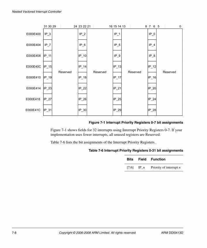
Nested Vectored Interrupt Controller
Figure 7-1 Interrupt Priority Registers 0-7 bit assignments
Figure 7-1 shows fields for 32 interrupts using Interrupt Priority Registers 0-7. If your implementation uses fewer interrupts, all unused registers are Reserved.
Table 7-6 lists the bit assignments of the Interrupt Priority Registers.
31 23 15 7 081624
E000E400
E000E404
E000E408
E000E40C
E000E410
E000E414
E000E418
E000E41C
561415 1322 212930
IP_0
IP_4
IP_8
IP_12
IP_16
IP_20
IP_24
IP_28
IP_1
IP_5
IP_9
IP_13
IP_17
IP_21
IP_25
IP_29
IP_2
IP_6
IP_10
IP_14
IP_18
IP_22
IP_26
IP_30
IP_3
IP_7
IP_11
IP_15
IP_19
IP_23
IP_27
IP_31
ReservedReservedReserved Reserved Reserved Reserved
Table 7-6 Interrupt Priority Registers 0-31 bit assignments
Bits Field Function
[7:6] IP_n Priority of interrupt n
7-8 Copyright © 2006-2008 ARM Limited. All rights reserved. ARM DDI0413D

Nested Vectored Interrupt Controller
7.3 Level versus pulse interrupts
The processor supports both level and pulse interrupts. A level interrupt is held asserted until it is cleared by the ISR accessing the device. A pulse interrupt is a variant of an edge model. The interrupt signal is sampled synchronously on the rising edge of the processor clock. The processor recognizes a pulse when the input is observed LOW and then HIGH on two consecutive rising edges of the processor clock.
For level interrupts, if the signal is not deasserted before the return from the interrupt routine, the interrupt repends and re-activates. This is particularly useful for FIFO and buffer-based devices because it ensures that they drain either by a single ISR or by repeated invocations, with no extra work. This means that the device holds the interrupt signal asserted until the device is empty.
A pulse interrupt must be asserted for at least one processor clock cycle to enable the NVIC to observe it.
A pulse interrupt can be reasserted during the ISR so that the interrupt can be pended and active at the same time. The application design must ensure that a second pulse does not arrive before the interrupt caused by the first pulse is activated. If the second pulse arrives before the interrupt is activated, the second pulse has no effect because it is already pended. When the ISR is activated, the pend bit is cleared. If the interrupt asserts again when the ISR is activated, the NVIC latches the pend bit again.
Pulse interrupts are mainly used for external signals and for rate or repeat signals.
ARM DDI0413D Copyright © 2006-2008 ARM Limited. All rights reserved. 7-9

Nested Vectored Interrupt Controller
7.4 Resampling level interrupts
An ISR can detect that no more interrupts occur during interrupt processing to avoid the overhead of ISR exit and entry. This information is available in the set and clear pending registers, see Interrupt Interrupt Set-Pending Register on page 7-5 and Interrupt Interrupt Clear-Pending Register on page 7-6.
For Pulse interrupts, a bit that is set to 1 indicates that another interrupt has arrived since the ISR started.
If the level interrupt is guaranteed to have been cleared and then asserted, the status bit read from the Interrupt Pending Registers is set to 1, as for pulse interrupts.
For level interrupts, where the line might remain HIGH continuously from ISR entry, write 1 to the appropriate bit of the:
• Interrupt Set-Pending Register
• Interrupt Clear-Pending Register.
The Interrupt Clear-Pending Register is not cleared if the interrupt line is HIGH, and can be read again to determine the status.
7-10 Copyright © 2006-2008 ARM Limited. All rights reserved. ARM DDI0413D

Nested Vectored Interrupt Controller
7.5 Interrupts as general purpose input
You can use an unused interrupt line as a general purpose input. To use the interrupt line as a general purpose input ensure the interrupt is disabled. See Interrupt Clear-Enable Register on page 7-4.
You can use the Interrupt Clear-Pending Register on page 7-6 to check if the input is HIGH since it was last accessed.
To check the current status, write 1 to the appropriate bit of Interrupt Clear-Pending Register. The value on the status bit is cleared if the interrupt line is LOW and the Interrupt Clear-Pending Register can be read again to determine the status.
ARM DDI0413D Copyright © 2006-2008 ARM Limited. All rights reserved. 7-11

Nested Vectored Interrupt Controller
7-12 Copyright © 2006-2008 ARM Limited. All rights reserved. ARM DDI0413D

Chapter 8 Debug
This chapter describes the debug system and how to use it. It contains the following sections:
• About debug on page 8-2
• Debug control on page 8-5
• ROM table on page 8-13
• BPU on page 8-16
• DW unit on page 8-19
• Debug TCM interface on page 8-24
• Examples of debug register halt, access, and step on page 8-25
• Data address watchpoint matching on page 8-28
• Semiprecise watchpoints on page 8-29.
ARM DDI0413D Copyright © 2006-2008 ARM Limited. All rights reserved. 8-1

Debug
8.1 About debug
There are two configurations for debug:
• The full debug configuration has four breakpoint comparators and two watchpoint comparators. This is the default configuration.
• The reduced debug configuration has two breakpoint comparators and one watchpoint comparator.
Debug facilitates:
• core halt
• core stepping
• core register access while halted
• read/write to:
— TCMs
— AHB address space
— internal Private Peripheral Bus (PPB)
• breakpoints
• watchpoints.
The main debug components are:
• debug control registers to access and control debugging of the core
• BreakPoint Unit (BPU) to implement breakpoints
• Data Watchpoint (DW) unit to implement watchpoints
• debug memory interfaces to access ITCM and DTCM
• ROM table.
All the debug components exist on the internal PPB, 0xE000ED30 - 0xE000EEFF. Access to the debug components is only possible when the debug extension is present.
Even when debug is present, you can only access the debug components from the debug port. Accesses from software are reserved.
Debug control and data access occurs through the Advanced High-performance Bus-Access Port (AHB-AP). This interface is driven by an external DP component. See Chapter 9 Debug Access Port for information on the AHB-AP and implementation options for the external DP component, typically a configurable SWJ-DP. Access includes:
• The AHB-PPB. Through this bus, the debugger can access debug, including:
— debug control
— DW unit
8-2 Copyright © 2006-2008 ARM Limited. All rights reserved. ARM DDI0413D

Debug
— BPU unit
— the ROM Table
— TCMs if configured.
• The AHB address space. The AHB slaves in the debug system always expect 32-bit AHB transfers. If a byte or halfword access is created from the DAP, the transfer is extended to a 32-bit access and all 32 bits in the register are accessed.
The DAP must be interpret all accesses as little-endian.
Figure 1-1 on page 1-4 shows the structure of the debug system, indicating how the AHB-AP can access each of the system components and external buses.
Table 8-1 shows a summary of the core debug registers.
Table 8-2 shows a summary of the Breakpoint registers.
Table 8-1 Core debug registers summary
Name Reset value Type Address Description
DFSR 0x0 R/W 0xE000ED30 See Debug Fault Status Register on page 8-5
DHCSR 0x0 R/W 0xE000EDF0 See Debug Halting Control and Status Register on page 8-7
DCRSR 0x0 WO 0xE000EDF4 See Debug Core Register Selector Register on page 8-10
DCRDR 0x0 R/W 0xE000EDF8 See Debug Core Register Data Register on page 8-11
DEMCR 0x0 R/W 0xE000EDFC See Debug Exception and Monitor Control Register on page 8-11
Table 8-2 BPU register summary
Name Reset value Type Address Description
BPU_CTRL 0x0 R/W 0xE0002000 See Breakpoint Control Register on page 8-16
BPU_COMP0 0x0 R/W 0xE0002008 See Breakpoint Comparator Registers on page 8-17
BPU_COMP1 0x0 R/W 0xE000200C See Breakpoint Comparator Registers on page 8-17
BPU_COMP2 0x0 R/W 0xE0002010 See Breakpoint Comparator Registers on page 8-17
BPU_COMP3 0x0 R/W 0xE0002014 See Breakpoint Comparator Registers on page 8-17
ARM DDI0413D Copyright © 2006-2008 ARM Limited. All rights reserved. 8-3
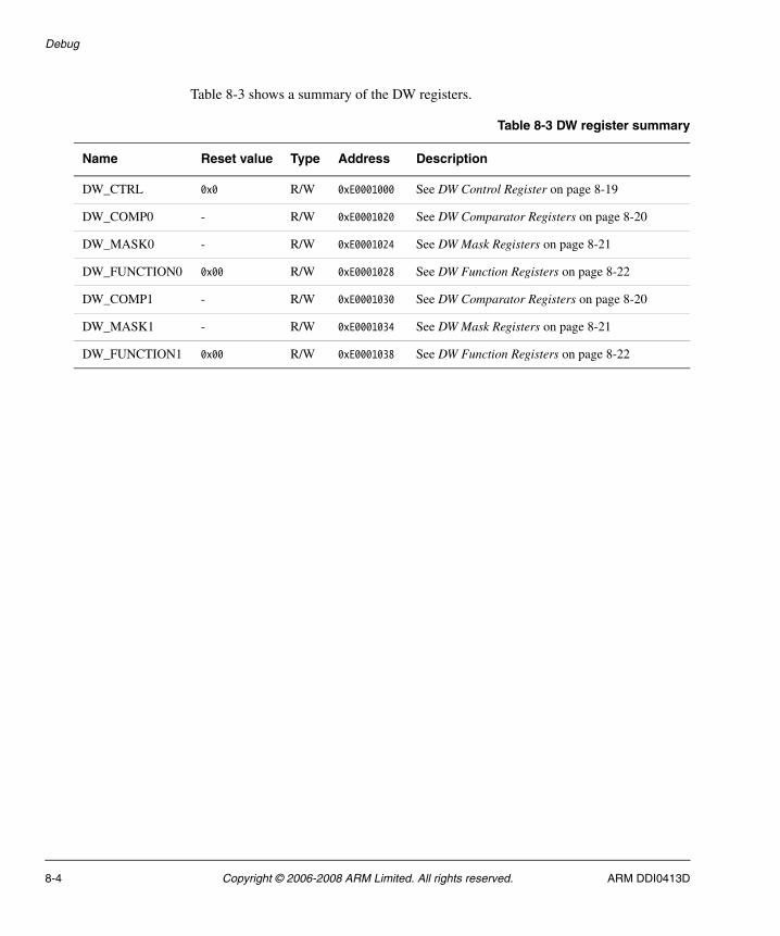
Debug
Table 8-3 shows a summary of the DW registers.
Table 8-3 DW register summary
Name Reset value Type Address Description
DW_CTRL 0x0 R/W 0xE0001000 See DW Control Register on page 8-19
DW_COMP0 - R/W 0xE0001020 See DW Comparator Registers on page 8-20
DW_MASK0 - R/W 0xE0001024 See DW Mask Registers on page 8-21
DW_FUNCTION0 0x00 R/W 0xE0001028 See DW Function Registers on page 8-22
DW_COMP1 - R/W 0xE0001030 See DW Comparator Registers on page 8-20
DW_MASK1 - R/W 0xE0001034 See DW Mask Registers on page 8-21
DW_FUNCTION1 0x00 R/W 0xE0001038 See DW Function Registers on page 8-22
8-4 Copyright © 2006-2008 ARM Limited. All rights reserved. ARM DDI0413D
Debug
8.2 Debug control
This section describes how to access and control core debug to test the core. It contains the following sections:
• Debug Fault Status Register
• Debug Halting Control and Status Register on page 8-7
• Debug Core Register Selector Register on page 8-10
• Debug Core Register Data Register on page 8-11
• Debug Exception and Monitor Control Register on page 8-11.
Note The processor cannot access the debug control register on the PPB. Accesses are Reserved if the processor attempts to access debug control. Debug control is accessed through the DAP.
8.2.1 Debug Fault Status Register
Use the Debug Fault Status Register (DSFR) to monitor:
• external debug requests
• vector catches
• data watchpoint match
• BKPT instruction execution and BPU comparator matches
• halt requests.
Multiple flags in the Debug Fault Status Register can be set when multiple debug conditions occur. The register is sticky read/write clear. This means that it can be read normally. Writing a 1 to a bit clears that bit.
C_DEBUGEN must be set before any bits in the DFSR are updated.
The register address, access type, and reset value are:
Address 0xE000ED30
Access Read/write-one-to-clear
Reset value 0x00000000
Figure 8-1 on page 8-6 shows the bit assignments of the Debug Fault Status Register.
ARM DDI0413D Copyright © 2006-2008 ARM Limited. All rights reserved. 8-5
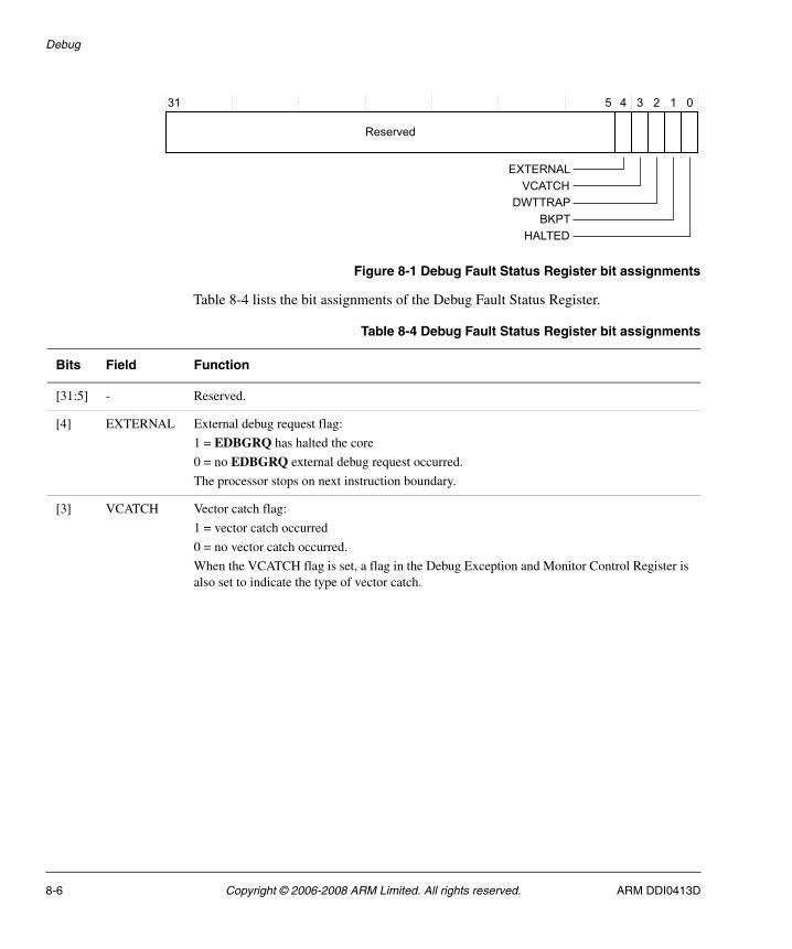
Debug
Figure 8-1 Debug Fault Status Register bit assignments
Table 8-4 lists the bit assignments of the Debug Fault Status Register.
31 4 3 2 1 0
Reserved
EXTERNALVCATCH
DWTTRAPBKPT
HALTED
5
Table 8-4 Debug Fault Status Register bit assignments
Bits Field Function
[31:5] - Reserved.
[4] EXTERNAL External debug request flag:
1 = EDBGRQ has halted the core
0 = no EDBGRQ external debug request occurred.
The processor stops on next instruction boundary.
[3] VCATCH Vector catch flag:
1 = vector catch occurred
0 = no vector catch occurred.
When the VCATCH flag is set, a flag in the Debug Exception and Monitor Control Register is also set to indicate the type of vector catch.
8-6 Copyright © 2006-2008 ARM Limited. All rights reserved. ARM DDI0413D

Debug
EXTERNAL, VCATCH, DWTRAP, BKPT, and HALTED are not set unless the event is caught. If C_DEBUGEN is enabled, these events halt the processor and cause it to enter Debug state.
8.2.2 Debug Halting Control and Status Register
The purpose of the Debug Halting Control and Status Register (DHCSR) is to:
• provide status information about the state of the processor
• enable core debug
• halt and step the processor.
The register address, access type, and reset value are:
Address 0xE000EDF0
Access Read/write
Reset value 0x20000000
Figure 8-2 on page 8-8 shows the bit assignments of the Debug Halting Control and Status Register.
[2] DWTRAP Data Watchpoint (DW) flag:
1 = DW match
0 = no DW match.
The processor stops at the current instruction or at the next instruction.
[1] BKPT BKPT flag:
1 = BKPT instruction or hardware breakpoint match
0 = no BKPT instruction or hardware breakpoint match.
The BKPT flag is set by the execution of the BKPT instruction or on an instruction whose address triggered the breakpoint comparator match. When the processor has halted, the return PC points to the address of the breakpointed instruction.
[0] HALTED Halt request flag:
1 = halt requested by DAP access to C_HALT or halted with C_STEP asserted
0 = no halt request.
Table 8-4 Debug Fault Status Register bit assignments (continued)
Bits Field Function
ARM DDI0413D Copyright © 2006-2008 ARM Limited. All rights reserved. 8-7
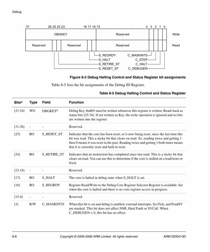
Debug
Figure 8-2 Debug Halting Control and Status Register bit assignments
Table 8-5 lists the bit assignments of the Debug ID Register.
Reserved
Reserved
DBGKEY
2 1 0341516171823242526
ReservedReserved
Write
Read
C_MASKINTSC_STEPC_HALT
C_DEBUGENS_RESET_STS_RETIRE_STS_HALTS_REGRDY
31
Table 8-5 Debug Halting Control and Status Register
Bitsa Type Field Function
[31:16] WO DBGKEYb Debug Key. 0xA05F must be written whenever this register is written. Reads back as status bits [25:16]. If not written as Key, the write operation is ignored and no bits are written into the register.
[31:26] - - Reserved.
[25] RO S_RESET_ST Indicates that the core has been reset, or is now being reset, since the last time this bit was read. This a sticky bit that clears on read. So, reading twice and getting 1 then 0 means it was reset in the past. Reading twice and getting 1 both times means that it is currently reset and held in reset.
[24] RO S_RETIRE_ST Indicates that an instruction has completed since last read. This is a sticky bit that clears on read. You can use this to determine if the core is stalled on a load/store or fetch.
[23:18] - - Reserved.
[17] RO S_HALT The core is halted in debug state when S_HALT is set.
[16] RO S_REGRDY Register Read/Write to the Debug Core Register Selector Register is available. Set when the core is halted and there is no core register access in progress.
[15:4] - - Reserved.
[3] R/W C_MASKINTS When this bit is set and debug is enabled, external interrupts, SysTick, and PendSV are masked. This bit does not affect NMI, Hard Fault or SVCall. When C_DEBUGEN = 0, this bit has no effect.
8-8 Copyright © 2006-2008 ARM Limited. All rights reserved. ARM DDI0413D

Debug
S_RETIRE_ST, S_HALT, S_REGRDY, and C_HALT always clear on a system reset. S_RESET_ST is always set on a system reset.
To halt on a reset, the following bits must be enabled:
• bit [0], VC_CORERESET, of the Debug Exception and Monitor Control Register
• bit [0], C_DEBUGEN, of the Debug Halting Control and Status Register.
When C_DEBUGEN is cleared it is recommended that you clear C_MASKINTS, C_STEP, and C_HALT in the same access.
You can only clear C_HALT from the debugger.
The following events can set C_HALT:
• Debugger write
• Watchpoint hit
• BKPT instruction or breakpoint hit
• C_STEP set and the processor has stepped an instruction
• EDBGRQ set
• reset vector catch
• hard fault vector catch.
Note • Only word accesses to the DHCSR are permitted.
• Non-word accesses are treated as if they were word accesses. If a byte or halfword access is created from the DAP, the transfer is extended to a 32-bit access and all 32 bits in the register are accessed.
[2] R/W C_STEP Steps the core in halted debug. When C_DEBUGEN = 0, this bit has no effect.
[1] R/W C_HALT Halts the core. This bit is set automatically when the core halts, for example, on a breakpoint. This bit clears on core reset. When C_DEBUGEN = 0, this bit has no effect.
[0] R/W C_DEBUGEN Enables or disable debug:
1 = debug enabled
0 = debug disabled.
a. Bits [3], [2], [0] are reset by DBGRESETn. Bits [25], [24], [17], [16], [1] are reset by SYSRESETn.b. Writes to this register with the wrong value in DBGKEY are ignored.
Table 8-5 Debug Halting Control and Status Register (continued)
Bitsa Type Field Function
ARM DDI0413D Copyright © 2006-2008 ARM Limited. All rights reserved. 8-9

Debug
8.2.3 Debug Core Register Selector Register
The purpose of the Debug Core Register Selector Register (DCRSR) is to select the processor register to transfer data to or from.
The register is 17 bits wide. The address and access type are:
Address 0xE000EDF4
Access Write-only
Figure 8-3 shows the bit assignments of the Debug Core Register Selector Register.
Figure 8-3 Debug Core Register Selector Register bit assignments
Table 8-6 lists the bit assignments of the Debug Core Selector Register.
REGSELReserved
REGWnR
Reserved
31 0151617 45
Table 8-6 Debug Core Register Selector Register
Bits Type Field Function
[31:17] - - Reserved
[16] WO REGWnR Write = 1
Read = 0
[15:5] - - Reserved
[4:0] WO REGSEL 5b00000 = R0
5b00001 = R1
…
5b01100 = R12
0b01101 = the current SP
0b01110 = LR
5b01111 = DebugReturnAddress()a
5b10000 = xPSR flags, execution number, and state information
5b10001 = MSP (Main SP)
5b10010 = PSP (Process SP)
0b10100 = {{6{1'b0}}, CONTROL[1], {24{1'b0}}, PRIMASK[0]}
All unused values are reserved.
8-10 Copyright © 2006-2008 ARM Limited. All rights reserved. ARM DDI0413D

Debug
This write-only register generates a request to the core to transfer data to or from Debug Core Register Data Register and the selected register. Until this core transaction is complete, bit [16], S_REGRDY, of the DHCSR is 0. You must ensure that S_REGRDY is HIGH before writing to the DCRSR.
Note • Writes to this register when C_DEBUGEN=0 are ignored.
• Writes other than word accesses are not permitted.
• Writes with REGSEL other than as indicated are not permitted.
• Reads from this register are not permitted.
• Writes to the IPSR are ignored.
• Bit[1] of the CONTROL register can only be set if the OS extension is present and the processor is in Thread mode.
8.2.4 Debug Core Register Data Register
The purpose of the Debug Core Register Data Register (DCRDR) is to hold data read from or written to core registers.
The register address, access type, and reset value are:
Address 0xE000EDF8
Access Read/write
Reset value 0x00000000
This is the data value written to the register selected by the Debug Register Selector Register.
8.2.5 Debug Exception and Monitor Control Register
The purpose of the Debug Exception and Monitor Control Register (DEMCR) is:
• Global enable for the DW unit.
• Vector catching. That is, causes debug entry on execution of a specified vector.
The register address, access type, and reset value are:
Address 0xE000EDFC
Access Read/write
a. This is the address of the next instruction to be executed. Bit [0] of DebugReturnAddress() is Reserved. Bit [0] does not affect the EPSR T-bit, which is accessed independently through the xPSR register selection. Modifying the T-bit in the EPSR has no effect on bit [0] of the DebugReturnAddress() so that the T-bit and DebugReturnAddress() might be modified in either order when changing between Thumb and ARM state while halted.
ARM DDI0413D Copyright © 2006-2008 ARM Limited. All rights reserved. 8-11
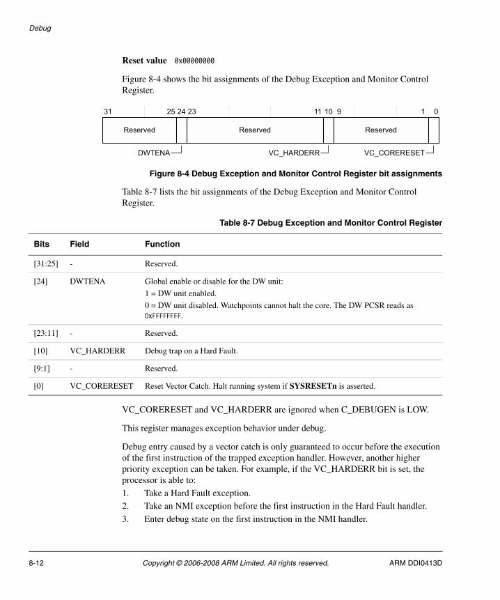
Debug
Reset value 0x00000000
Figure 8-4 shows the bit assignments of the Debug Exception and Monitor Control Register.
Figure 8-4 Debug Exception and Monitor Control Register bit assignments
Table 8-7 lists the bit assignments of the Debug Exception and Monitor Control Register.
VC_CORERESET and VC_HARDERR are ignored when C_DEBUGEN is LOW.
This register manages exception behavior under debug.
Debug entry caused by a vector catch is only guaranteed to occur before the execution of the first instruction of the trapped exception handler. However, another higher priority exception can be taken. For example, if the VC_HARDERR bit is set, the processor is able to:
1. Take a Hard Fault exception.
2. Take an NMI exception before the first instruction in the Hard Fault handler.
3. Enter debug state on the first instruction in the NMI handler.
ReservedReserved Reserved
31 1 0
DWTENA
91011232425
VC_HARDERR VC_CORERESET
Table 8-7 Debug Exception and Monitor Control Register
Bits Field Function
[31:25] - Reserved.
[24] DWTENA Global enable or disable for the DW unit:
1 = DW unit enabled.
0 = DW unit disabled. Watchpoints cannot halt the core. The DW PCSR reads as OxFFFFFFFF.
[23:11] - Reserved.
[10] VC_HARDERR Debug trap on a Hard Fault.
[9:1] - Reserved.
[0] VC_CORERESET Reset Vector Catch. Halt running system if SYSRESETn is asserted.
8-12 Copyright © 2006-2008 ARM Limited. All rights reserved. ARM DDI0413D

Debug
8.3 ROM table
Table 8-8 shows the memory-mapped registers in ROM memory and the general format of the component ID and peripheral ID registers. For more information on the ROM table, see the ARMv6-M Architecture Reference Manual.
Table 8-8 ROM memory
Address Value Name Bits Description
0xE00FF000 0xFFF0F003 SCS [31:0] Points to the System Control Space (SCS) at 0xE000E000. This includes core debug control registers.
0xE00FF004 0xFFF02003 DW [31:0] Points to the DW unit at 0xE0001000.
0xE00FF008 0xFFF03003 BPU [31:0] Points to the BPU at 0xE0002000.
0xE00FF00C 0x00000000 end [31:0] Marks of end of table. Because adding more debug components is not permitted, this value is fixed.
0xE00FFFCC 0x00000001 MEMTYPE [7:0] System memory map is always accessible from the DAP. Always set to 0x1.
0xE00FFFD0 0x00000004 Peripheral ID4 [31:8] Reserved.
[7:4] Indicates the size of the ROM table:
0x0 = 4KB ROM table.
[3:0] JEP106 continuation code:
0x4
0xE00FFFD4 0x00000000 Peripheral ID5 - Reserved.
0xE00FFFD8 0x00000000 Peripheral ID6 -
0xE00FFFDC 0x00000000 Peripheral ID7 -
0xE00FFFE0 0x00000070 Peripheral ID0 [31:8] Reserved.
[7:0] Contains bits [7:0] of the part number:
0x70.
0xE00FFFE4 0x000000B4 Peripheral ID1 [31:8] Reserved.
[7:4] Contains bits [3:0] of the JEP106 ID code:
0xB.
[3:0] Contains bits [11:8] of the part number
0x4.
ARM DDI0413D Copyright © 2006-2008 ARM Limited. All rights reserved. 8-13

Debug
Note The complete:
• JEP106 continuation code is 0x4
• JEP106 ID code for ARM is 0x3B
0xE00FFFE8 0x0000002B Peripheral ID2 [31:8] Reserved.
[7:4] Indicates the revision:
0x0 = r0p0
0x1 = r0p1
0x2 = r1p0.
[3] Indicates JEDEC assigned ID fields:
0x1.
[2:0] Contains bits [6:4] of the JEP106 ID code:
0x3.
0xE00FFFEC 0x00000000 Peripheral ID3 [31:8] Reserved.
[7:4] Indicates minor revision field RevAnd.
[3:0] Indicates block unmodified:
0x0.
0xE00FFFF0 0x0000000D Component ID0 [31:8] Reserved.
[7:0] Preamblea.
0xE00FFFF4 0x00000010 Component ID1 [31:8] Reserved.
[7:4] Indicates component class:
0x1 = ROM table.
[3:0] Preamblea.
0xE00FFFF8 0x00000005 Component ID2 [31:8] Reserved.
[7:0] Preamblea.
0xE00FFFFC 0x000000B1 Component ID3 [31:8] Reserved.
[7:0] Preamblea.
a. Preamble enables a debugger to detect the presence of the ROM table.
Table 8-8 ROM memory (continued)
Address Value Name Bits Description
8-14 Copyright © 2006-2008 ARM Limited. All rights reserved. ARM DDI0413D

Debug
• The Cortex-M1 processor part number is 0x470.
ARM DDI0413D Copyright © 2006-2008 ARM Limited. All rights reserved. 8-15

Debug
8.4 BPU
The BPU implements:
• four instruction comparators in the full debug configuration
• two instruction comparators in the reduced debug configuration.
You can configure each instruction comparator to provide a hardware breakpoint.
The registers that provide BPU operations are:
• Breakpoint Control Register
• Breakpoint Comparator Registers on page 8-17.
A BP comparator register matching the address of the second half word of a 32-bit instruction generates the breakpoint.
8.4.1 Breakpoint Control Register
Use the Breakpoint Control Register to enable the Breakpoint block.
The register address, access type, and reset value are:
Address 0xE0002000
Access Read/write
Reset value Bit [0] (ENABLE) is reset to b0.
Figure 8-5 shows the bit assignments of the Breakpoint Control Register.
Figure 8-5 Breakpoint Control Register bit assignments
31 3 2 1 0
Reserved
478
NUM_CODE1
ENABLEKEY
Reserved
8-16 Copyright © 2006-2008 ARM Limited. All rights reserved. ARM DDI0413D

Debug
Table 8-9 lists the bit assignments of the Breakpoint Control Register.
8.4.2 Breakpoint Comparator Registers
Use the Breakpoint Comparator Registers to store the values to compare with the instruction address.
In the full debug configuration the register address, access type, and reset value are:
Address 0xE0002008, 0xE000200C, 0xE0002010, and 0xE0002014
Access Read/write
Reset value Bit [0] (ENABLE) is reset to b0.
In the reduced debug configuration the register address, access type, and reset value are:
Address 0xE0002008, 0xE000200C
Access Read/write
Reset value Bit [0] (ENABLE) is reset to b0.
Figure 8-6 on page 8-18 shows the bit assignments of the Breakpoint Comparator Registers.
Table 8-9 Breakpoint Control Register bit assignments
Bits Field Type Function
[31:8] - RO Reserved.
[7:4] NUM_CODE1 RO Number of comparators. This read-only field and contains either:
b0100 = four instruction comparators in use
b0010 = two instruction comparators in use.
[3:2] - RO Reserved.
[1] KEY WO Key field. To write to the Breakpoint Control Register, you must write a 1 to this write-only bit. This bit is reads as zero.
[0] ENABLE R/W Breakpoint unit enable bit:
1 = Breakpoint unit enabled
0 = Breakpoint unit disabled.
DBGRESETn clears the ENABLE bit.
ARM DDI0413D Copyright © 2006-2008 ARM Limited. All rights reserved. 8-17

Debug
Figure 8-6 Breakpoint Comparator Registers bit assignments
Table 8-10 lists the bit assignments of the Breakpoint Comparator Registers.
31 0
COMP
12829 230
ReservedBP_MATCH ENABLE
Reserved
Table 8-10 Breakpoint Comparator Registers bit assignments
Bits Field Function
[31:30] BP_MATCH This field selects what happens when the COMP address is matched.It is interpreted as:
b00 = no breakpoint matching
b01 = set breakpoint on lower halfword, upper is unaffected
b10 = set breakpoint on upper halfword, lower is unaffected
b11 = set breakpoint on both lower and upper halfwords.
[29] - Reserved.
[28:2] COMP Comparison address. Although it is architecturally Unpredictable whether breakpoint matches on the address of the second halfword of a 32-bit instruction to generate a debug event, in this processor it is predictable and a debug event is generated.
[1] - Reserved.
[0] ENABLE Compare enable for Breakpoint Comparator Register n:
1 = Breakpoint Comparator Register n compare enabled
0 = Breakpoint Comparator Register n compare disabled.
The ENABLE bit of BPU_CTRL must also be set to enable comparisons.
DBGRESETn clears the ENABLE bit.
8-18 Copyright © 2006-2008 ARM Limited. All rights reserved. ARM DDI0413D

Debug
8.5 DW unit
The DW unit implements:
• two comparators in the full debug configuration
• one comparator in the reduced debug configuration.
Each set of comparators contains:
• a comparator register, see DW Comparator Registers on page 8-20
• a mask register, see DW Mask Registers on page 8-21
• a function register, see DW Function Registers on page 8-22
You can configure each set of a comparators as a:
• PC hardware watchpoint
• data address watchpoint.
You can also read sampled PC values from the DW unit.
Note The information in this section is for both the full and reduced debug configuration unless otherwise stated.
8.5.1 DW Control Register
Use the DW Control Register to check how many comparators are available.
The register address, access type, and reset value are:
Address 0xE0001000
Access Read-only
Reset value 0x20000000
Figure 8-7 shows the bit assignments of the DW Control Register.
Figure 8-7 DW Control Register bit assignments
31 028 27
NUMCOMP Reserved
ARM DDI0413D Copyright © 2006-2008 ARM Limited. All rights reserved. 8-19
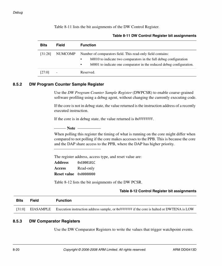
Debug
Table 8-11 lists the bit assignments of the DW Control Register.
8.5.2 DW Program Counter Sample Register
Use the DW Program Counter Sample Register (DWPCSR) to enable coarse-grained software profiling using a debug agent, without changing the currently executing code.
If the core is not in debug state, the value returned is the instruction address of a recently executed instruction.
If the core is in debug state, the value returned is 0xFFFFFFFF.
Note When polling this register the timing of what is running on the core might differ when compared to not polling if the core makes accesses to the PPB. This is because the core and the DAP share access to the PPB, where the DAP has higher priority.
The register address, access type, and reset value are:
Address 0xE000101C
Access Read-only
Reset value 0x00000000
Table 8-12 lists the bit assignments of the DW PCSR.
8.5.3 DW Comparator Registers
Use the DW Comparator Registers to write the values that trigger watchpoint events.
Table 8-11 DW Control Register bit assignments
Bits Field Function
[31:28] NUMCOMP Number of comparators field. This read-only field contains:
• b0010 to indicate two comparators in the full debug configuration
• b0001 to indicate one comparator in the reduced debug configuration.
[27:0] - Reserved.
Table 8-12 Control Register bit assignments
Bits Field Function
[31:0] EIASAMPLE Execution instruction address sample, or 0xFFFFFFFF if the core is halted or DWTENA is LOW
8-20 Copyright © 2006-2008 ARM Limited. All rights reserved. ARM DDI0413D

Debug
In the full debug configuration the register address, access type, and reset value are:
Address 0xE0001020, 0xE0001030
Access Read/write
Reset value 0x00000000
In the reduced debug configuration the register address, access type, and reset value are:
Address 0xE0001020
Access Read/write
Reset value 0x00000000
Table 8-13 describes the field of DW Comparator Registers.
8.5.4 DW Mask Registers
Use the DW Mask Registers to apply a mask to data addresses when matching against COMP.
In the full debug configuration the register address, access type, and reset value are:
Address 0xE0001024, 0xE0001034
Access Read/write
Reset value 0x00000000
In the reduced debug configuration the register address, access type, and reset value are:
Address 0xE0001024
Access Read/write
Reset value 0x00000000
Figure 8-8 shows the bit assignments of DW Mask Registers.
Figure 8-8 DW Mask Registers 0-1 format
Table 8-13 DW Comparator Registers bit assignments
Field Name Definition
[31:0] COMP DW_COMP to compare against PC or the data address as given by DW_FUNCTION Register.
DW_COMP is always masked using the DW Mask Register value before a compare is done.
31 0
Reserved
4
MASK
3
ARM DDI0413D Copyright © 2006-2008 ARM Limited. All rights reserved. 8-21
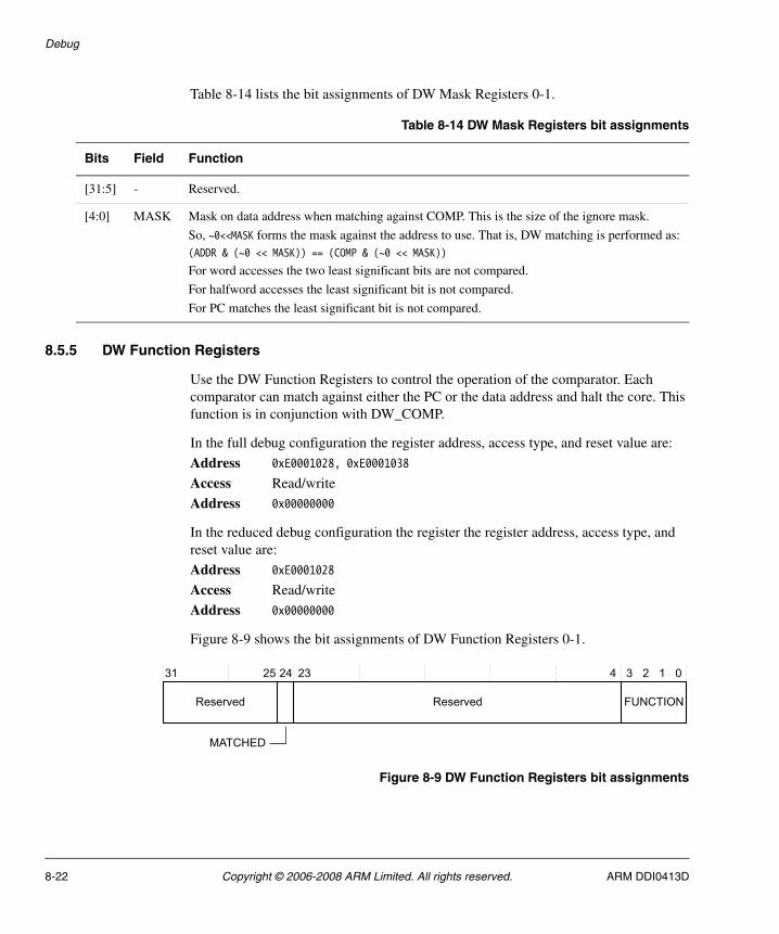
Debug
Table 8-14 lists the bit assignments of DW Mask Registers 0-1.
8.5.5 DW Function Registers
Use the DW Function Registers to control the operation of the comparator. Each comparator can match against either the PC or the data address and halt the core. This function is in conjunction with DW_COMP.
In the full debug configuration the register address, access type, and reset value are:
Address 0xE0001028, 0xE0001038
Access Read/write
Address 0x00000000
In the reduced debug configuration the register the register address, access type, and reset value are:
Address 0xE0001028
Access Read/write
Address 0x00000000
Figure 8-9 shows the bit assignments of DW Function Registers 0-1.
Figure 8-9 DW Function Registers bit assignments
Table 8-14 DW Mask Registers bit assignments
Bits Field Function
[31:5] - Reserved.
[4:0] MASK Mask on data address when matching against COMP. This is the size of the ignore mask.
So, ~0<<MASK forms the mask against the address to use. That is, DW matching is performed as:(ADDR & (~0 << MASK)) == (COMP & (~0 << MASK))
For word accesses the two least significant bits are not compared.
For halfword accesses the least significant bit is not compared.
For PC matches the least significant bit is not compared.
31 1 04 3 2
Reserved FUNCTION
25 24 23
MATCHED
Reserved
8-22 Copyright © 2006-2008 ARM Limited. All rights reserved. ARM DDI0413D
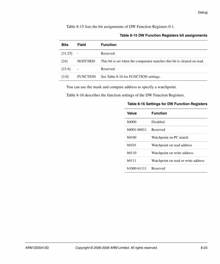
Debug
Table 8-15 lists the bit assignments of DW Function Registers 0-1.
You can use the mask and compare address to specify a watchpoint.
Table 8-16 describes the function settings of the DW Function Registers.
Table 8-15 DW Function Registers bit assignments
Bits Field Function
[31:25] - Reserved.
[24] MATCHED This bit is set when the comparator matches this bit is cleared on read.
[23:4] - Reserved.
[3:0] FUNCTION See Table 8-16 for FUNCTION settings.
Table 8-16 Settings for DW Function Registers
Value Function
b0000 Disabled
b0001-b0011 Reserved
b0100 Watchpoint on PC match
b0101 Watchpoint on read address
b0110 Watchpoint on write address
b0111 Watchpoint on read or write address
b1000-b1111 Reserved
ARM DDI0413D Copyright © 2006-2008 ARM Limited. All rights reserved. 8-23

Debug
8.6 Debug TCM interface
The Debug TCM interface comprises a DTCM and an ITCM interface.
The static signals CFGITCMSZ[3:0] and CFGDTCMSZ[3:0] indicate the size of ITCM and DTCM:
• ITCM address range is from 0x00000000 to the size specified by CFGITCMSZ[3:0]
• DTCM address range is from 0x20000000 to the size specified by CFGDTCMSZ[3:0].
If an AHB access from the AHB-AP is:
• inside the configured TCM range the access is to the appropriate TCM
• outside the configured TCM range the access is to the external interface as appropriate.
Note Unless the core is halted or held in reset by SYSRESETn, any debug access to the TCM memory might conflict with core operation.
8-24 Copyright © 2006-2008 ARM Limited. All rights reserved. ARM DDI0413D

Debug
8.7 Examples of debug register halt, access, and step
This section provides example sequences that you can use to perform debug register access, halt, step, and exit.
8.7.1 Debug halt example
This is an example of a debug halt. If you want to halt the processor, perform the following:
1. Write 0xA05F0003 to the Debug Halting Control and Status Register. This enables debug and halts the core.
2. Wait for the S_HALT bit of the DHCSR to be set. This indicates that the core is halted.
8.7.2 Debug read register access example
This is an example of a debug read register access. If you want to halt the processor and read a value from one of the core registers, perform the following:
1. Write 0xA05F0003 to the Debug Halting Control and Status Register. This enables debug and halts the core.
2. Wait for the S_HALT bit of the Debug Halting Control and Status Register to be set. This indicates that the core is halted.
3. Write the register number that you want to read into the Debug Core Register Selector Register and set bit [16] to 0 simultaneously.
4. Wait for the S_REGRDY bit in the DHCSR to set. This indicates the core has completed the read master.
5. Read the DCRDR. This returns the required core register.
8.7.3 Debug write register access example
This is an example of a debug register access. If you want to halt the processor and write a value into one of the registers, perform the following:
1. Write 0xA05F0003 to the Debug Halting Control and Status register. This enables debug and halts the core.
2. Wait for the S_HALT bit of the Debug Halting Control and Status Register to be set. This indicates that the core is halted.
3. Write the value that you want to be written to the DCRDR.
ARM DDI0413D Copyright © 2006-2008 ARM Limited. All rights reserved. 8-25

Debug
4. Write the register number that you want to write to into the Debug Core Register Selector Register and set bit [16] to 0 simultaneously.
5. Wait for the S_REGRDY bit in the DCRSR to be set. This indicates the core has completed the write transfer.
8.7.4 Debug step example
This is an example of a debug step. If you want to step the processor, perform the following:
1. Write 0xA05F0003 to the Debug Halting Control and Status Register. This enables debug and halts the core.
2. Wait for S_HALT to be set one in the DHCSR to indicate that the core is halted.
3. Write 0xA05F0005 to the Debug Halting Control and Status Register. This clears C_HALT and sets C_STEP to one.
4. The core exits debug state, executes one instruction and returns to halted debug state.
5. The core remains halted in debug state.
If more single steps are required repeat steps 3-5.
Note When entering debug halt step, you can set C_DEBUGEN, C_HALT and C_STEP in one write instruction.
8.7.5 Breakpoint debug entry example
This is an example of a hardware PC breakpoint using the BPU. If you want to halt the processor with a breakpoint, perform the following:
1. Write 0xA05F0001 to the DHCSR to set C_DEBUGEN to enable debug.
2. Set the value in BU_COMP0 register to the address of the instruction that you want to set as a breakpoint to break the execution flow.
3. Use BU_CTRL to enable the breakpoint.
4. C_HALT is set by the hardware when the hardware breakpoint matches.
5. Read S_HALT to ensure the core is halted.
8-26 Copyright © 2006-2008 ARM Limited. All rights reserved. ARM DDI0413D
Debug
8.7.6 Exiting core debug
You can exit Halting debug by:
• clearing the C_DEBUGEN and C_HALT bits in the Debug Halting Control and Status Register.
• using the DBGRESTART/DBGRESTARTED handshake interface.
See the ARMv6-M Architecture Reference Manual for more details.
ARM DDI0413D Copyright © 2006-2008 ARM Limited. All rights reserved. 8-27
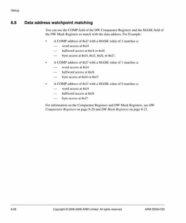
Debug
8.8 Data address watchpoint matching
You can use the COMP field of the DW Comparator Registers and the MASK field of the DW Mask Registers to match with the data address. For Example:
• A COMP address of 0x27 with a MASK value of 2 matches a:
— word access at 0x24
— halfword access at 0x24 or 0x26
— byte access at 0x24, 0x25, 0x26, or 0x27.
• A COMP address of 0x27 with a MASK value of 1 matches a:
— word access at 0x24
— halfword access at 0x26
— byte access at 0x26 or 0x27.
• A COMP address of 0x27 with a MASK value of 0 matches a:
— word access at 0x24
— halfword access at 0x26
— byte access at 0x27.
For information on the Comparator Registers and DW Mask Registers, see DW Comparator Registers on page 8-20 and DW Mask Registers on page 8-21.
8-28 Copyright © 2006-2008 ARM Limited. All rights reserved. ARM DDI0413D

Debug
8.9 Semiprecise watchpoints
The processor watchpoints are described as semiprecise. When the processor triggers a watchpoint, it executes one more instruction after the one that triggered the watchpoint, before entering debug state. The number of extra instructions is constant, independent of bus or instruction cycle times. If another debug event causes the processor to enter debug state earlier, for example as a result of a breakpoint, the processor enters debug state with more than one flag set in the DFSR. See Debug Fault Status Register on page 8-5 for more information.
Note The instruction executed can include an exception return sequence or any number of exception entry sequences.
ARM DDI0413D Copyright © 2006-2008 ARM Limited. All rights reserved. 8-29

Debug
8-30 Copyright © 2006-2008 ARM Limited. All rights reserved. ARM DDI0413D
Chapter 9 Debug Access Port
This chapter describes the processor Debug Access Port (DAP). It contains:
• About the DAP on page 9-2
• Debug access on page 9-3
• AHB-AP on page 9-5.
ARM DDI0413D Copyright © 2006-2008 ARM Limited. All rights reserved. 9-1

Debug Access Port
9.1 About the DAP
When debug is implemented, the processor also contains an Advanced High-performance Bus Access Port (AHB-AP) interface for debug accesses.
External DP components access this AHB-AP interface. The Cortex-M1 system supports three possible DP implementations:
• Serial Wire JTAG Debug Port (SWJ-DP). This is a standard CoreSight debug port that combines JTAG-DP and the Serial Wire Debug Port (SW-DP) and allows switching between Serial Wire and JTAG.
• Only SW-DP, through configuration options.
• Only JTAG-DP, through configuration options
The DP and AP together are referred to as the Debug Access Port (DAP).
Figure 9-1 shows the DAP configuration.
Figure 9-1 DAP configuration
For additional information about the DP components, see the CoreSight Components Technical Reference Manual.
For more information on the AHB-AP, see AHB-AP on page 9-5.
Note If your implementation of the DAP does not include both JTAG-DP and SW-DP, you cannot switch between them.
SWJ-DP
DAP internal interface AHB-AP interfaceDebug port
interface
JTAG-DP
SW-DP
Cortex-M1
AHB-AP
DAP
9-2 Copyright © 2006-2008 ARM Limited. All rights reserved. ARM DDI0413D
Debug Access Port
9.2 Debug access
The SWJ-DP and AHB-AP enables access to the debug system and core components of the processor over the AHB matrix. The access to the memory map from the DAP is the same as that made by data accesses from the core, although this is restricted to always be little-endian. The PPB, TCMs and external AHB interface are accessible.
9.2.1 Debug access during core reset
To enable access to the debug modules at all times, all processor debug logic is reset by the DBGRESETn signal instead of the SYSRESETn signal. The debug interface and debug access logic are accessible when SYSRESETn is asserted.
When SYSRESETn is asserted:
• debug writes to non-debug components, including the core registers, have no effect
• debug reads from non-debug components, including the core registers, return unpredictable data.
• accesses from the DAP to the system AHB bus through the AHB Matrix complete, but the returned read data is unpredictable.
9.2.2 Debug access while core running
Arbitration between the core and debug is so that DAP accesses always have priority. This means that polling for an event using the DAP is always possible, but might change the precise cycle timing of core accesses.
ARM DDI0413D Copyright © 2006-2008 ARM Limited. All rights reserved. 9-3
Debug Access Port
9.2.3 Debug access to TCMs
Caution • Only use a debugger to write to TCMs when the core is halted.
• Although a debugger can perform debug accesses to TCM when the core is running, some FPGA RAM implementations might have unpredictable results when a read and write occur simultaneously to the same location. If this is the case, you must ensure logic is included to prevent accesses occurring simultaneously.
The core of the processor has a single address for each TCM for both reads and writes to enable a non-debug processor to use single-ported RAMs. You can use dual-port RAMs for TCMs to enable programming before the core of the processor is removed from reset and to facilitate debug removal.
For information on TCM sizes, see Table 10-3 on page 10-7.
9-4 Copyright © 2006-2008 ARM Limited. All rights reserved. ARM DDI0413D
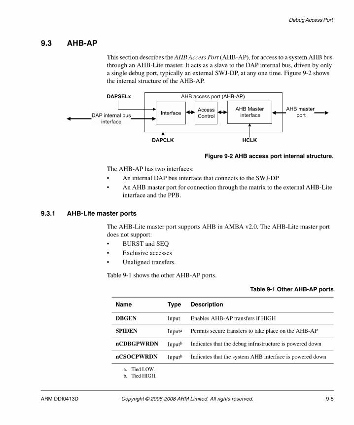
Debug Access Port
9.3 AHB-AP
This section describes the AHB Access Port (AHB-AP), for access to a system AHB bus through an AHB-Lite master. It acts as a slave to the DAP internal bus, driven by only a single debug port, typically an external SWJ-DP, at any one time. Figure 9-2 shows the internal structure of the AHB-AP.
Figure 9-2 AHB access port internal structure.
The AHB-AP has two interfaces:
• An internal DAP bus interface that connects to the SWJ-DP
• An AHB master port for connection through the matrix to the external AHB-Lite interface and the PPB.
9.3.1 AHB-Lite master ports
The AHB-Lite master port supports AHB in AMBA v2.0. The AHB-Lite master port does not support:
• BURST and SEQ
• Exclusive accesses
• Unaligned transfers.
Table 9-1 shows the other AHB-AP ports.
Interface Access Control
AHB master port
DAPCLK
DAP internal businterface
AHB Master interface
HCLK
DAPSELx AHB access port (AHB-AP)
Table 9-1 Other AHB-AP ports
Name Type Description
DBGEN Input Enables AHB-AP transfers if HIGH
SPIDEN Inputa
a. Tied LOW.
Permits secure transfers to take place on the AHB-AP
nCDBGPWRDN Inputb
b. Tied HIGH.
Indicates that the debug infrastructure is powered down
nCSOCPWRDN Inputb Indicates that the system AHB interface is powered down
ARM DDI0413D Copyright © 2006-2008 ARM Limited. All rights reserved. 9-5

Debug Access Port
9.3.2 AHB-AP programmer’s model
This section describes the registers used to program the AHB-AP:
• AHB-AP register summary
• AHB access port register descriptions.
AHB-AP register summary
Table 9-2 shows the AHB access port registers.
AHB access port register descriptions
The section describes the AHB access port registers:
• AHB-AP Control/Status Word Register, CSW, 0x00 on page 9-7
• AHB-AP Transfer Address Register, TAR, 0x04 on page 9-8
• AHB-AP Data Read/Write Register, DRW, 0x0C on page 9-9
• AHB-AP Banked Data Registers, BD0-BD03, 0x10-Ox1C on page 9-9
• ROM Address Register, ROM, 0xF8 on page 9-10
• AHB-AP Identification Register, IDR, 0xFC on page 9-10.
Table 9-2 AHB access port registers
Offset Type Width Reset value Name
0x00 R/W 32 0x43800042 Control/Status Word, CSW
0x04 R/W 32 0x00000000 Transfer Address, TAR
0x08 - - - Reserved SBZ
0x0C R/W 32 - Data Read/Write, DRW
0x10 R/W 32 - Banked Data 0, BD0
0x14 R/W 32 - Banked Data 1, BD1
0x18 R/W 32 - Banked Data 2, BD2
0x1C R/W 32 - Banked Data 3, BD3
0x20-0xF7 - - - Reserved SBZ
0xF8 RO 32 0xE00FF000 Debug ROM table
0xFC RO 32 0x44770001 Identification Register, IDR
9-6 Copyright © 2006-2008 ARM Limited. All rights reserved. ARM DDI0413D

Debug Access Port
AHB-AP Control/Status Word Register, CSW, 0x00
This is the control word used to configure and control transfers through the AHB interface.
Figure 9-3 shows the Control/Status Word Register bit assignments.
Figure 9-3 AHB-AP Control/Status Word Register bit assignments
Table 9-3 lists the bit assignments.
Size
31 28 24 23 12 11 8 7 6 5 4 3 2 0
Prot Reserved Mode
TrInProgDbgStatus
AddrIncReserved
Reserved SPIStatus
2227
Table 9-3 AHB-AP Control/Status Word Register bit assignments
Bits Type Name Function
[31] - - Reserved SBZ.
[30] - - Reserved SB0.
[29:28] - - Reserved SBZ.
[27:24] R/W Prot Specifies the protection signal encoding to be output on HPROT[3:0].Reset value is noncacheable, non-bufferable, data access, privileged = b0011.
[23] RO SPIStatus Indicates the status of the SPIDEN port. Always reads as b1.
[22:12] - - Reserved SBZ.
[11:8] R/W Mode Specifies the mode of operation:
b0000 = Normal download/upload model
b0001-b1111 = Reserved SBZ.
Reset value = b0000.
[7] RO TrInProg Transfer in progress. This field indicates if a transfer is currently in progress on the AHB master port.
[6] RO DbgStatus Indicates the status of the DBGEN port. Always reads as b1 = AHB transfers permitted.
ARM DDI0413D Copyright © 2006-2008 ARM Limited. All rights reserved. 9-7

Debug Access Port
AHB-AP Transfer Address Register, TAR, 0x04
Table 9-4 shows the AHB-AP Transfer Address Register bit assignments.
[5:4] R/W AddrInc Auto address increment and packing mode on Read or Write data access. Only increments if the current transaction completes without an Error Response. Does not increment if the transaction completes with an Error Response or the transaction is aborted.
Auto address incrementing and packed transfers are not performed on access to Banked Data registers 0x10-0x1C. The status of these bits is ignored in these cases.
Increments and wraps within a 1KB address boundary, for example, for word incrementing from 0x1400-0x17FC. If the start is at 0x14A0, then the counter increments to 0x17FC, wraps to 0x1400, then continues incrementing to 0x149C.
b00 = auto increment off
b01 = increment, single.
Single transfer from corresponding byte lane.
b10 = increment, packed
Word = same effect as single increment.
Byte/Halfword. Packs four 8-bit transfers or two 16-bit transfers into a 32-bit DAP transfer. Multiple transactions are carried out on the AHB interface.
b11 = Reserved SBZ, no transfer.
Size of address increment is defined by the Size field, bits [2:0].
Reset value = b00.
[3] - - Reserved SBZ, R/W = b0
[2:0] R/W Size Size of the data access to perform:
b000 = 8 bits
b001 = 16 bits
b010 = 32 bits
b011-b111 = Reserved SBZ.
Reset value = b010.
Table 9-3 AHB-AP Control/Status Word Register bit assignments (continued)
Bits Type Name Function
Table 9-4 AHB-AP Transfer Address Register bit assignments
Bits Type Name Function
[31:0] R/W Address Address of the current transfer. Unaligned address values with respect to the Size field of the Control/Status Word Register are unsupported.
Reset value is 0x00000000.
9-8 Copyright © 2006-2008 ARM Limited. All rights reserved. ARM DDI0413D
Debug Access Port
AHB-AP Data Read/Write Register, DRW, 0x0C
Table 9-5 shows the AHB-AP Data Read/Write Register bit assignments.
AHB-AP Banked Data Registers, BD0-BD03, 0x10-Ox1C
BD0-BD3 provide a mechanism for directly mapping through DAP accesses to AHB transfers without having to rewrite the Transfer Address Register (TAR) within a four-location boundary. BD0 reads/writes from TA. BD1 reads/writes from TA+4. Table 9-6 shows the AHB-AP Banked Data Register bit assignments.
Table 9-5 AHB-AP Data Read/Write Register bit assignments
Bits Type Name Function
[31:0] R/W Data Write mode:
Data value to write for the current transfer.
Read mode:
Data value read from the current transfer.
Table 9-6 Banked Data Register bit assignments
Bits Type Name Function
[31:0] R/W Data If DAPADDR[7:4] = 0x0001, so accessing AHB-AP registers in the range 0x10-0x1C, the derived HADDR[31:0] is:
• Write mode:
Data value to write for the current transfer to external address TAR[31:4] + DAPADDR[3:2] + 2'b00.
• Read mode:
Data value read from the current transfer from external address TAR[31:4] + DAPADDR[3:2] + 2'b00.
Auto address incrementing is not performed on DAP accesses to BD0-BD3.
Banked transfers are only supported for word transfers. Non-word banked transfers are reserved and Unpredictable. Transfer size is currently ignored for banked transfers.
ARM DDI0413D Copyright © 2006-2008 ARM Limited. All rights reserved. 9-9

Debug Access Port
ROM Address Register, ROM, 0xF8
Table 9-7 shows the ROM Address Register bit assignments.
AHB-AP Identification Register, IDR, 0xFC
The register reset value is 0x447700001.
Figure 9-4 shows the AHB-AP Identification Register bit assignments.
Figure 9-4 AHB-AP Identification Register bit assignments
Table 9-8 shows the AHB-AP Identification Register bit assignments.
Table 9-7 ROM Address Register bit assignments
Bits Type Name Function
[31:0] RO Debug AHB ROM Address Base address of a ROM table. The ROM provides a look-up table for system components. Set to 0xE00FF000 in the AHB-AP in the initial release.
Revision
31 28 27 24 23 17 16 15 8 7 0
JEDEC bank JEDEC code Reserved Identity value
AP
Table 9-8 AHB-AP Identification Register bit assignments
Bits Type Name
[31:28] RO Revision. Reset value is 0x2 for AHB-AP.
[27:24] RO JEDEC banka. Reset value is 0x4.
a. Using JEDEC bank 0x0 with a JEDEC code of 0x00 is reserved for use by ARM.
[23:17] RO JEDEC code. Reset value is 0x3B.
[16] RO ARM AP. Reset value is b1.
[15:8] - Reserved SBZ.
[7:0] RO Identity value. Reset value is 0x01 for AHB-AP.
9-10 Copyright © 2006-2008 ARM Limited. All rights reserved. ARM DDI0413D

Debug Access Port
9.3.3 AHB-AP clocks and resets
The AHB-AP has two clock domains:
DAPCLK Drives the DAP bus interface and access control for register read and writes. DAPCLK must be driven by a constant clock. When started, it must not be stopped or altered while the DAP is in use.
DAPCLK can be connected to HCLK or can be asynchronous to HCLK, if there are other APs in the SoC that cannot operate at full HCLK.
HCLK AHB clock domain driving AHB interface.
DAPRESETn
Initializes the state of all registers in the AHB-AP.
9.3.4 Supported AHB protocol features
The AHB-Lite master port supports AHB in AMBA v2.0.
HPROT encodings
HPROT[3:0] is provided as an external port and is programmed from the Prot field in the CSW register with the following conditions:
• HPROT[3:0] programming is supported.
• Exclusive access is not supported, so HRESP[2] is not supported.
See AHB-AP Control/Status Word Register, CSW, 0x00 on page 9-7 for values of the Prot field.
HRESP
HRESP[0] is the only RESPONSE signal required by the AHB-AP:
• AHB-Lite devices do not support SPLIT and RETRY and so HRESP[1] is not required.
• HRESP[2] is not supported in the AHB-AP.
ARM DDI0413D Copyright © 2006-2008 ARM Limited. All rights reserved. 9-11

Debug Access Port
AHB-AP transfer types and bursts
The AHB-AP cannot initiate a new AHB transfer every clock cycle (unpacked) because of the additional cycles required to serial scan in the new address or data value through a debug port. The AHB-AP supports two HTRANS transfer types, IDLE and NONSEQ.
• When a transfer is in progress, it is of type NONSEQ.
• When no transfer is in progress and the AHB-AP is still granted the bus then the transfer is of type IDLE.
The only unpacked HBURST encoding supported is SINGLE. Packed 8-bit transfers or 16-bit transfers are treated as individual NONSEQ, SINGLE transfers at the AHB-Lite interface. This ensures that there are no issues with boundary wrapping, to avoid additional AHB-AP complexity.
9.3.5 Packed transfers
The DAP internal interface is a 32-bit data bus. 8-bit or 16-bit transfers can be formed on AHB according to the Size field in the Control/Status Word Register at 0x00. The AddrInc field in the Control/Status Word Register enables optimized use of the DAP internal bus to reduce the number of accesses from the tools to the DAP. It indicates if the entire data word is to be used to pack more than one transfer. Address incrementing is automatically enabled if packet transfers are initiated so that multiple transfers are carried out at the sequential addresses. The size of the address increment is based on the size of the transfer.
See AHB-AP Control/Status Word Register, CSW, 0x00 on page 9-7 for values of the AddrInc field and AHB-AP Data Read/Write Register, DRW, 0x0C on page 9-9 for Data Read/Write Register bit values.
Examples of the transactions are:
• For an unpacked 16-bit write to an address base of 0x2 (CSW[2:0]=b001, CSW[5:4]=b01), HWDATA[31:16] is written from bits [31:16] in the Data Read/Write Register.
• For an unpacked 8-bit read to an address base of 0x1, (CSW[2:0]=b000, CSW[5:4]=b01), HRDATA[31:16] and HRDATA[7:0] are zeroed and HRDATA[15:8] contains read data.
• For a packed byte write at a base address 0x2, (CSW[2:0]=b000, CSW[5:4]=b10), four write transfers are initiated, the order of data being sent is:
— HWDATA[23:16], from DRW[23:16], to HADDR[31:0]=0x2
— HWDATA[31:24], from DRW[31:24], to HADDR[31:0]=0x3
9-12 Copyright © 2006-2008 ARM Limited. All rights reserved. ARM DDI0413D

Debug Access Port
— HWDATA[7:0], from DRW[7:0], to HADDR[31:0]=0x4
— HWDATA[15:8], from DRW[15:8], to HADDR[31:0]=0x5
• For a packed halfword reading at a base address of 0x2, (CSW[2:0]=b001, CSW[5:4]=b10), two read transfers are initiated:
— HRDATA[31:16] is stored into DRW[31:16] from HADDR[31:0]=0x2
— HRDATA[15:0] is stored into DRW[15:0] from HADDR[31:0]=0x4
If the current transfer is aborted or the current transfer receives an ERROR response, the AHB-AP does not complete the following packed transfers.
ARM DDI0413D Copyright © 2006-2008 ARM Limited. All rights reserved. 9-13

Debug Access Port
9-14 Copyright © 2006-2008 ARM Limited. All rights reserved. ARM DDI0413D

Chapter 10 External and Memory Interfaces
This chapter describes the processor external and memory interfaces. It contains the following sections:
• About bus interfaces on page 10-2
• External interface on page 10-3
• Write buffer on page 10-4
• Memory attributes on page 10-5
• Memory interfaces on page 10-6.
ARM DDI0413D Copyright © 2006-2008 ARM Limited. All rights reserved. 10-1

External and Memory Interfaces
10.1 About bus interfaces
The processor contains two bus interfaces:
• external interface
• memory interfaces.
Note The processor contains an internal PPB for accesses to the Nested Vectored Interrupt Controller (NVIC), Data Watchpoint (DW) unit, and BreakPoint Unit (BPU).
10-2 Copyright © 2006-2008 ARM Limited. All rights reserved. ARM DDI0413D

External and Memory Interfaces
10.2 External interface
This is an AHB-Lite bus interface. See External AHB-Lite interface on page A-5 for descriptions of the AHB-lite bus signals.
Processor accesses and debug accesses to external AHB peripherals are implemented over this bus. Because processor AHB access to zero wait state slaves typically take two cycles longer than TCM accesses, instructions and data must be contained in TCM where possible. If on-chip FPGA memory is used for the processor, highest performance is possible if this is TCM memory, rather than SRAM mapped onto the AHB interface.
Processor accesses and debug accesses share the external interface. Debug accesses take priority over processor accesses.
Timing of processor accesses might be changed by the presence of debug accesses. Giving highest priority to debug means that debug cannot be locked-out by a continuously executing stream of core instructions. Because debug accesses tend to be infrequent, debug accesses do not have a major impact on processor accesses.
Any vendor specific components can populate this bus.
If an external AHB peripheral incorrectly deadlocks the AHB bus, the debugger might not be able to halt or access the core registers. Contact your implementation team for FPGA probing tools to debug the system external to the core.
Unaligned accesses to this bus are not supported.
ARM DDI0413D Copyright © 2006-2008 ARM Limited. All rights reserved. 10-3

External and Memory Interfaces
10.3 Write buffer
To prevent bus wait cycles from stalling the processor during data stores, stores to the external interfaces go through a one-entry write buffer. If the write buffer is full, subsequent accesses to the bus stall until the write buffer has drained.
DMB and DSB instructions wait for the write buffer to drain before completing.
10-4 Copyright © 2006-2008 ARM Limited. All rights reserved. ARM DDI0413D
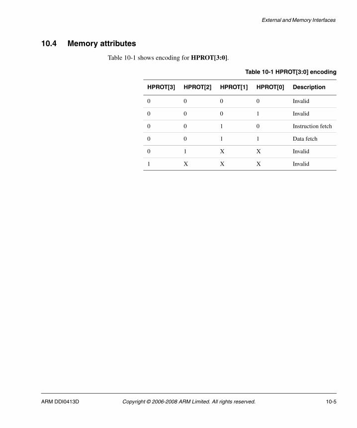
External and Memory Interfaces
10.4 Memory attributes
Table 10-1 shows encoding for HPROT[3:0].
Table 10-1 HPROT[3:0] encoding
HPROT[3] HPROT[2] HPROT[1] HPROT[0] Description
0 0 0 0 Invalid
0 0 0 1 Invalid
0 0 1 0 Instruction fetch
0 0 1 1 Data fetch
0 1 X X Invalid
1 X X X Invalid
ARM DDI0413D Copyright © 2006-2008 ARM Limited. All rights reserved. 10-5
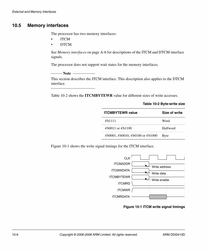
External and Memory Interfaces
10.5 Memory interfaces
The processor has two memory interfaces:
• ITCM
• DTCM.
See Memory interfaces on page A-6 for descriptions of the ITCM and DTCM interface signals.
The processor does not support wait states for the memory interfaces.
Note This section describes the ITCM interface. This description also applies to the DTCM interface.
Table 10-2 shows the ITCMBYTEWR value for different sizes of write accesses.
Figure 10-1 shows the write signal timings for the ITCM interface.
Figure 10-1 ITCM write signal timings
Table 10-2 Byte-write size
ITCMBYTEWR value Size of write
4'b1111 Word
4'b0011 or 4'b1100 Halfword
4'b0001, 4'b0010, 4'b0100 or 4'b1000 Byte
CLK
ITCMADDR
ITCMWDATA
ITCMBYTEWR
ITCMRD
ITCMWR
ITCMRDATA
Write address
Write data
Write enable
10-6 Copyright © 2006-2008 ARM Limited. All rights reserved. ARM DDI0413D

External and Memory Interfaces
For writes, the write address, write data, and control signals are driven on the same cycle. The write enable signals ensure individual bytes within a word are written without corrupting the other bytes in the same word. For example, if ITCMBYTEWR[1] is asserted, bits ITCMBYTEWR[15:8] are written in to byte 1 of the word at address ITCMADRR.
Figure 10-1 on page 10-6 shows the read signal timings for the ITCM interface.
Figure 10-2 ITCM read signal timings
Table 10-3 shows the TCM sizes that are defined through input pins. These sizes are factored into both the core and debug address decoders.
0
CLK
ITCMADDR
ITCMWDATA
ITCMBYTEWR
ITCMRD
ITCMWR
ITCMRDATA
Read address
Read data
Table 10-3 Instruction and Data TCM sizes
CFGITCMSZE or CFGDTCMSZE
TCM size
4'h0 0KB
4'h1 1KB
4'h2 2KB
4'h3 4KB
4'h4 8KB
4'h5 16KB
4'h6 32KB
4'h7 64KB
4'h8 128KB
ARM DDI0413D Copyright © 2006-2008 ARM Limited. All rights reserved. 10-7
External and Memory Interfaces
If you use other values than those that Table 10-3 on page 10-7 shows, the effects are Unpredictable.
4'h9 256KB
4'hA 512KB
4'hB 1MB
Table 10-3 Instruction and Data TCM sizes (continued)
CFGITCMSZE or CFGDTCMSZE
TCM size
10-8 Copyright © 2006-2008 ARM Limited. All rights reserved. ARM DDI0413D

Appendix A Signal Descriptions
This appendix lists the processor interfaces and the interface signals. Full description of an interface or signal is given where the interfaces or signals differ from those described in the appropriate interface specification. It contains the following sections:
• Clocks and Resets on page A-2
• Miscellaneous on page A-3
• Interrupt interface on page A-4
• External AHB-Lite interface on page A-5
• Memory interfaces on page A-6
• AHB-AP interface on page A-9.
ARM DDI0413D Copyright © 2006-2008 ARM Limited. All rights reserved. A-1
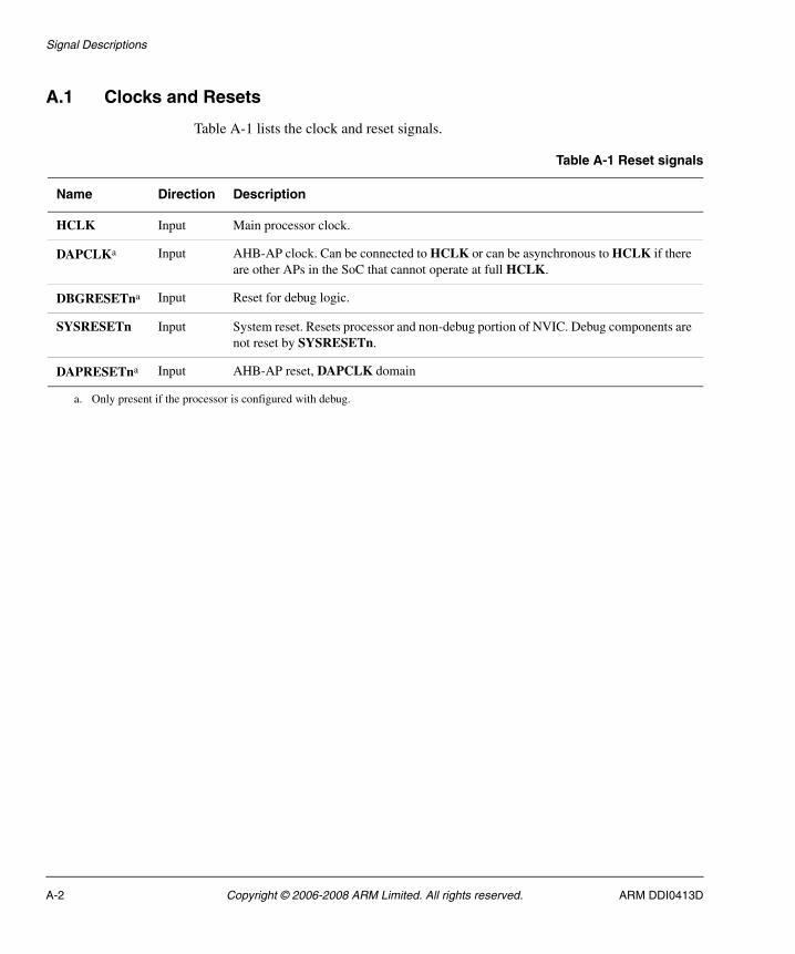
Signal Descriptions
A.1 Clocks and Resets
Table A-1 lists the clock and reset signals.
Table A-1 Reset signals
Name Direction Description
HCLK Input Main processor clock.
DAPCLKa Input AHB-AP clock. Can be connected to HCLK or can be asynchronous to HCLK if there are other APs in the SoC that cannot operate at full HCLK.
DBGRESETna Input Reset for debug logic.
SYSRESETn Input System reset. Resets processor and non-debug portion of NVIC. Debug components are not reset by SYSRESETn.
DAPRESETna Input AHB-AP reset, DAPCLK domain
a. Only present if the processor is configured with debug.
A-2 Copyright © 2006-2008 ARM Limited. All rights reserved. ARM DDI0413D
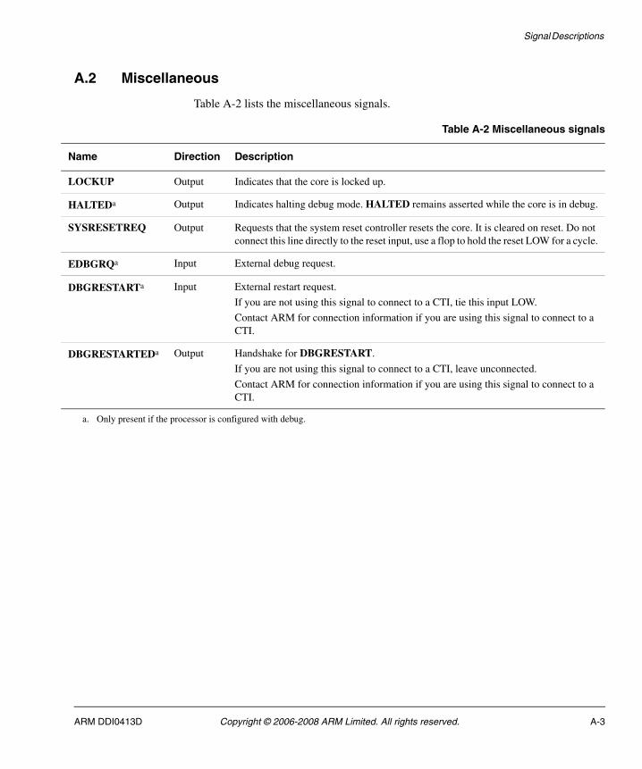
Signal Descriptions
A.2 Miscellaneous
Table A-2 lists the miscellaneous signals.
Table A-2 Miscellaneous signals
Name Direction Description
LOCKUP Output Indicates that the core is locked up.
HALTEDa Output Indicates halting debug mode. HALTED remains asserted while the core is in debug.
SYSRESETREQ Output Requests that the system reset controller resets the core. It is cleared on reset. Do not connect this line directly to the reset input, use a flop to hold the reset LOW for a cycle.
EDBGRQa Input External debug request.
DBGRESTARTa Input External restart request.
If you are not using this signal to connect to a CTI, tie this input LOW.
Contact ARM for connection information if you are using this signal to connect to a CTI.
DBGRESTARTEDa Output Handshake for DBGRESTART.
If you are not using this signal to connect to a CTI, leave unconnected.
Contact ARM for connection information if you are using this signal to connect to a CTI.
a. Only present if the processor is configured with debug.
ARM DDI0413D Copyright © 2006-2008 ARM Limited. All rights reserved. A-3
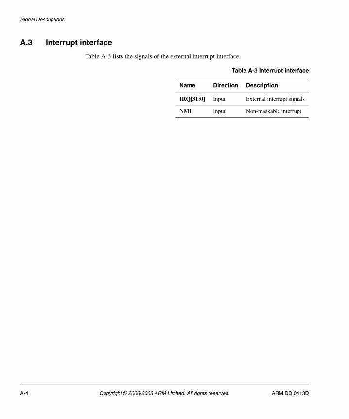
Signal Descriptions
A.3 Interrupt interface
Table A-3 lists the signals of the external interrupt interface.
Table A-3 Interrupt interface
Name Direction Description
IRQ[31:0] Input External interrupt signals
NMI Input Non-maskable interrupt
A-4 Copyright © 2006-2008 ARM Limited. All rights reserved. ARM DDI0413D

Signal Descriptions
A.4 External AHB-Lite interface
Table A-4 lists the signals of the external AHB-Lite interface.
Table A-4 External AHB-Lite interface
Name Direction Description
HADDR[31:0] Output For more information, see the AMBA 3 AHB-Lite Protocol Specification
HBURST[2:0] Output
HPROT[3:0] Output
HRDATA[31:0] Input
HREADY Input
HRESP Input
HSIZE[2:0] Output
HTRANS[1:0] Output
HWDATA[31:0] Output
HWRITE Output
ARM DDI0413D Copyright © 2006-2008 ARM Limited. All rights reserved. A-5

Signal Descriptions
A.5 Memory interfaces
Table A-5 lists the signals of the ITCM interface.
Table A-6 lists the signals of the DTCM interface.
Table A-5 ITCM interface
Name Direction Description
ITCMEN Output Enable to memory. Either ITCMRD or ITCMWR is also set.
ITCMRD Output Read Enable to memory, set only if ITCMEN is set.
ITCMWR Output Write Enable, set if and only if ITCMBYTEWR is non zero, and only if ITCMEN is set.
ITCMBYTEWR[3:0] Output Write Enables for each byte, if any of these are set, ITCMWR is also set.
ITCMADDR[19:2] Output Address to read from or write to.
ITCMWDATA[31:0] Output Data to be written to ITCM. Only bytes that ITCMBYTEWR is set for are valid.
ITCMRDATA[31:0] Input Data read from the ITCMADDR. All reads are 32 bit.
CFGITCMSZ[3:0] Input Size encoded onto 4 bits. Tie off at synthesis time to optimize logic for speed, or wire to a static value at run time to permit more flexibility.
CFGITCMEN[1:0] Input ITCM Alias Enables. Sets the value written into the Upper and Lower ITCM Alias Enable bits in the Auxiliary Control Register on reset.
CFGITCMEN[1] sets the Upper Alias Enable bit and CFGITCMEN[0] sets the Lower Alias Enable bit.
The value on these pins must be held constant for at least 2 cycles before SYSRESETn is deasserted.
Table A-6 DTCM interface
Name Direction Description
DTCMEN Output Enable to memory. Either DTCMRD or DTCMWR is also set.
DTCMRD Output Read Enable to memory, set only if DTCMEN is set.
DTCMWR Output Write Enable, set if and only if DTCMBYTEWR is non zero, and only if DTCMEN is set.
DTCMBYTEWR[3:0] Output Write Enables for each byte. If any of these are set, DTCMWR is also set.
DTCMADDR[19:2] Output Address to read from or write to.
A-6 Copyright © 2006-2008 ARM Limited. All rights reserved. ARM DDI0413D
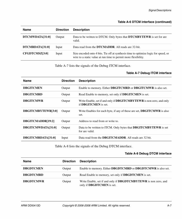
Signal Descriptions
Table A-7 lists the signals of the Debug ITCM interface.
Table A-8 lists the signals of the Debug DTCM interface.
DTCMWDATA[31:0] Output Data to be written to DTCM. Only bytes that DTCMBYTEWR is set for are valid.
DTCMRDATA[31:0] Input Data read from the DTCMADDR. All reads are 32-bit.
CFGDTCMSZ[3:0] Input Size encoded onto 4 bits. Tie off at synthesis time to optimize logic for speed, or wire to a static value at run time to permit more flexibility.
Table A-6 DTCM interface (continued)
Name Direction Description
Table A-7 Debug ITCM interface
Name Direction Description
DBGITCMEN Output Enable to memory. Either DBGITCMRD or DBGITCMWR is also set.
DBGITCMRD Output Read Enable to memory, set only if DBGITCMEN is set.
DBGITCMWR Output Write Enable, set if and only if DBGITCMBYTEWR is non zero, and only if DBGITCMEN is set.
DBGITCMBYTEWR[3:0] Output Write Enables for each byte, if any of these are set, DBGITCMWR is also set.
DBGITCMADDR[19:2] Output Address to read from or write to.
DBGITCMWDATA[31:0] Output Data to be written to ITCM. Only bytes that DBGITCMBYTEWR is set for are valid.
DBGITCMRDATA[31:0] Input Data read from the DBGITCMADDR. All reads are 32 bit.
Table A-8 Debug DTCM interface
Name Direction Description
DBGDTCMEN Output Enable to memory. Either DBGDTCMRD or DBGDTCMWR is also set.
DBGDTCMRD Output Read Enable to memory, set only if DBGDTCMEN is set.
DBGDTCMWR Output Write Enable, set if and only if DBGDTCMBYTEWR is non zero, and only if DBGDTCMEN is set.
ARM DDI0413D Copyright © 2006-2008 ARM Limited. All rights reserved. A-7
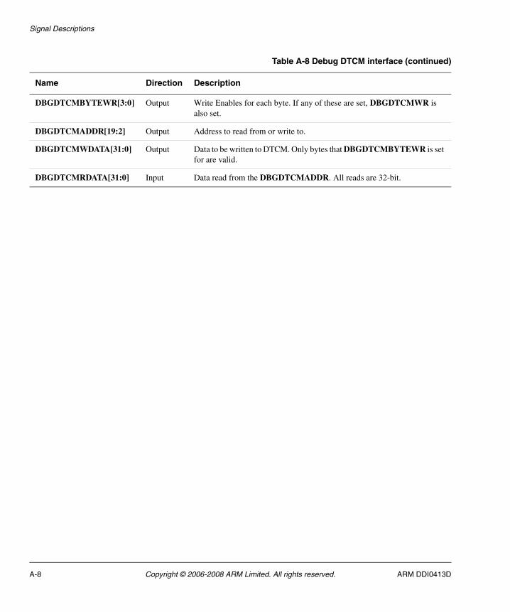
Signal Descriptions
DBGDTCMBYTEWR[3:0] Output Write Enables for each byte. If any of these are set, DBGDTCMWR is also set.
DBGDTCMADDR[19:2] Output Address to read from or write to.
DBGDTCMWDATA[31:0] Output Data to be written to DTCM. Only bytes that DBGDTCMBYTEWR is set for are valid.
DBGDTCMRDATA[31:0] Input Data read from the DBGDTCMADDR. All reads are 32-bit.
Table A-8 Debug DTCM interface (continued)
Name Direction Description
A-8 Copyright © 2006-2008 ARM Limited. All rights reserved. ARM DDI0413D
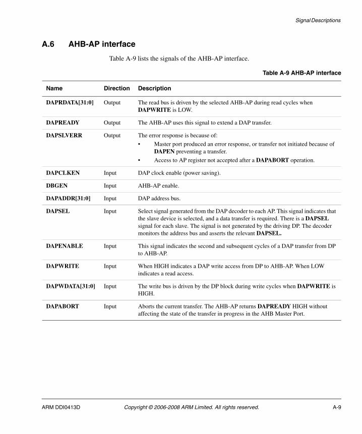
Signal Descriptions
A.6 AHB-AP interface
Table A-9 lists the signals of the AHB-AP interface.
Table A-9 AHB-AP interface
Name Direction Description
DAPRDATA[31:0] Output The read bus is driven by the selected AHB-AP during read cycles when DAPWRITE is LOW.
DAPREADY Output The AHB-AP uses this signal to extend a DAP transfer.
DAPSLVERR Output The error response is because of:
• Master port produced an error response, or transfer not initiated because of DAPEN preventing a transfer.
• Access to AP register not accepted after a DAPABORT operation.
DAPCLKEN Input DAP clock enable (power saving).
DBGEN Input AHB-AP enable.
DAPADDR[31:0] Input DAP address bus.
DAPSEL Input Select signal generated from the DAP decoder to each AP. This signal indicates that the slave device is selected, and a data transfer is required. There is a DAPSEL signal for each slave. The signal is not generated by the driving DP. The decoder monitors the address bus and asserts the relevant DAPSEL.
DAPENABLE Input This signal indicates the second and subsequent cycles of a DAP transfer from DP to AHB-AP.
DAPWRITE Input When HIGH indicates a DAP write access from DP to AHB-AP. When LOW indicates a read access.
DAPWDATA[31:0] Input The write bus is driven by the DP block during write cycles when DAPWRITE is HIGH.
DAPABORT Input Aborts the current transfer. The AHB-AP returns DAPREADY HIGH without affecting the state of the transfer in progress in the AHB Master Port.
ARM DDI0413D Copyright © 2006-2008 ARM Limited. All rights reserved. A-9

Signal Descriptions
A-10 Copyright © 2006-2008 ARM Limited. All rights reserved. ARM DDI0413D

Glossary
This glossary describes some of the terms used in technical documents from ARM Limited.
Abort A mechanism that indicates to a core that the attempted memory access is invalid or not allowed or that the data returned by the memory access is invalid. An abort can be caused by the external or internal memory system as a result of attempting to access invalid or protected instruction or data memory.
See also Data Abort, External Abort and Prefetch Abort.
Addressing modes Various mechanisms, shared by many different instructions, for generating values used by the instructions.
Advanced High-performance Bus (AHB)A bus protocol with a fixed pipeline between address/control and data phases. It only supports a subset of the functionality provided by the AMBA AXI protocol. The full AMBA AHB protocol specification includes a number of features that are not commonly required for master and slave IP developments and ARM Limited recommends only a subset of the protocol is usually used. This subset is defined as the AMBA AHB-Lite protocol.
See also Advanced Microcontroller Bus Architecture and AHB-Lite.
ARM DDI0413D Copyright © 2006-2008 ARM Limited. All rights reserved. Glossary-1
Glossary
Advanced Microcontroller Bus Architecture (AMBA)A family of protocol specifications that describe a strategy for the interconnect. AMBA is the ARM open standard for on-chip buses. It is an on-chip bus specification that details a strategy for the interconnection and management of functional blocks that make up a System-on-Chip (SoC). It aids in the development of embedded processors with one or more CPUs or signal processors and multiple peripherals. AMBA complements a reusable design methodology by defining a common backbone for SoC modules.
Advanced Peripheral Bus (APB)A simpler bus protocol than AXI and AHB. It is designed for use with ancillary or general-purpose peripherals such as timers, interrupt controllers, UARTs, and I/O ports. Connection to the main system bus is through a system-to-peripheral bus bridge that helps to reduce system power consumption.
AHB See Advanced High-performance Bus.
AHB Access Port (AHB-AP)An optional component of the DAP that provides an AHB interface to a SoC.
AHB-AP See AHB Access Port.
AHB-Lite A subset of the full AMBA AHB protocol specification. It provides all of the basic functions required by the majority of AMBA AHB slave and master designs, particularly when used with a multi-layer AMBA interconnect. In most cases, the extra facilities provided by a full AMBA AHB interface are implemented more efficiently by using an AMBA AXI protocol interface.
Aligned A data item stored at an address that is divisible by the number of bytes that defines the data size is said to be aligned. Aligned words and halfwords have addresses that are divisible by four and two respectively. The terms word-aligned and halfword-aligned therefore stipulate addresses that are divisible by four and two respectively.
AMBA See Advanced Microcontroller Bus Architecture.
APB See Advanced Peripheral Bus.
Architecture The organization of hardware and/or software that characterizes a processor and its attached components, and enables devices with similar characteristics to be grouped together when describing their behavior, for example, Harvard architecture, instruction set architecture, ARMv6-M architecture.
ARM instruction An instruction of the ARM Instruction Set Architecture (ISA). These cannot be executed by the processor.
ARM state The processor state in which the processor executes the instructions of the ARM ISA. The processor only operates in Thumb state, never in ARM state.
Glossary-2 Copyright © 2006-2008 ARM Limited. All rights reserved. ARM DDI0413D
Glossary
Base register A register specified by a load or store instruction that is used to hold the base value for the instruction’s address calculation. Depending on the instruction and its addressing mode, an offset can be added to or subtracted from the base register value to form the address that is sent to memory.
Base register write-backUpdating the contents of the base register used in an instruction target address calculation so that the modified address is changed to the next higher or lower sequential address in memory. This means that it is not necessary to fetch the target address for successive instruction transfers and enables faster burst accesses to sequential memory.
Beat Alternative word for an individual data transfer within a burst. For example, an INCR4 burst comprises four beats.
BE-8 Big-endian view of memory in a byte-invariant system.
See also LE, Byte-invariant and Word-invariant.
Big-endian Byte ordering scheme in which bytes of decreasing significance in a data word are stored at increasing addresses in memory.
See also Little-endian and Endianness.
Big-endian memory Memory in which:
• a byte or halfword at a word-aligned address is the most significant byte or halfword within the word at that address
• a byte at a halfword-aligned address is the most significant byte within the halfword at that address.
See also Little-endian memory.
Breakpoint A breakpoint is a mechanism provided by debuggers to identify an instruction at which program execution is to be halted. Breakpoints are inserted by the programmer to enable inspection of register contents, memory locations, variable values at fixed points in the program execution to test that the program is operating correctly. Breakpoints can be removed after the program is successfully tested.
See also Watchpoint.
ARM DDI0413D Copyright © 2006-2008 ARM Limited. All rights reserved. Glossary-3
Glossary
Burst A group of transfers to consecutive addresses. Because the addresses are consecutive, there is no requirement to supply an address for any of the transfers after the first one. This increases the speed at which the group of transfers can occur. Bursts over AMBA are controlled using signals to indicate the length of the burst and how the addresses are incremented.
See also Beat.
Byte An 8-bit data item.
Byte-invariant In a byte-invariant system, the address of each byte of memory remains unchanged when switching between little-endian and big-endian operation. When a data item larger than a byte is loaded from or stored to memory, the bytes making up that data item are arranged into the correct order depending on the endianness of the memory access. The ARM architecture supports byte-invariant systems in ARMv6 and later versions.
See also Word-invariant.
Cold reset Also known as power-on reset.
See also Warm reset.
Context The environment that each process operates in for a multitasking operating system.
Core A core is that part of a processor that contains the ALU, the datapath, the general-purpose registers, the Program Counter, and the instruction decode and control circuitry.
Core reset See Warm reset.
Data Abort An indication from a memory system to the core of an attempt to access an illegal data memory location. An exception must be taken if the processor attempts to use the data that caused the abort.
See also Abort.
Debug Access Port (DAP)A TAP block that acts as an AMBA, AHB or AHB-Lite, master for access to a system bus. The DAP is the term used to encompass a set of modular blocks that support system wide debug. The DAP is a modular component, intended to be extendable to support optional access to multiple systems such as memory mapped AHB and APB through a single debug interface.
Debugger A debugging system that includes a program, used to detect, locate, and correct software faults, together with custom hardware that supports software debugging.
Glossary-4 Copyright © 2006-2008 ARM Limited. All rights reserved. ARM DDI0413D

Glossary
Endianness Byte ordering. The scheme that determines the order that successive bytes of a data word are stored in memory. An aspect of the system’s memory mapping.
See also Little-endian and Big-endian
Exception An error or event which can cause the processor to suspend the currently executing instruction stream and execute a specific exception handler or interrupt service routine. The exception could be an external interrupt or NMI, or it could be a fault or error event that is considered serious enough to require that program execution is interrupted. Examples include attempting to perform an invalid memory access, external interrupts, and undefined instructions. When an exception occurs, normal program flow is interrupted and execution is resumed at the corresponding exception vector. This contains the first instruction of the interrupt service routine to deal with the exception.
Exception handlerSee Interrupt service routine.
Exception vector See Interrupt vector.
Halfword A 16-bit data item.
Halt mode One of two mutually exclusive debug modes. In halt mode all processor execution halts when a breakpoint or watchpoint is encountered. All processor state, coprocessor state, memory and input/output locations can be examined and altered by the JTAG interface.
See also Monitor debug-mode.
Host A computer that provides data and other services to another computer. Especially, a computer providing debugging services to a target being debugged.
Implementation-definedThe behavior is not architecturally defined, but is defined and documented by individual implementations.
Internal PPB See Private Peripheral Bus.
Interrupt service routine
A program that control of the processor is passed to when an interrupt occurs.
Interrupt vector One of a number of fixed addresses in low memory that contains the first instruction of the corresponding interrupt service routine.
Joint Test Action Group (JTAG)The name of the organization that developed standard IEEE 1149.1. This standard defines a boundary-scan architecture used for in-circuit testing of integrated circuit devices. It is commonly known by the initials JTAG.
JTAG See Joint Test Action Group.
ARM DDI0413D Copyright © 2006-2008 ARM Limited. All rights reserved. Glossary-5

Glossary
JTAG Debug Port (JTAG-DP)An optional external interface for the DAP that provides a standard JTAG interface for debug access.
JTAG-DP See JTAG Debug Port.
LE Little endian view of memory in both byte-invariant and word-invariant systems. See also Byte-invariant, Word-invariant.
Little-endian Byte ordering scheme in which bytes of increasing significance in a data word are stored at increasing addresses in memory.
See also Big-endian and Endianness.
Little-endian memoryMemory in which:
• a byte or halfword at a word-aligned address is the least significant byte or halfword within the word at that address
• a byte at a halfword-aligned address is the least significant byte within the halfword at that address.
See also Big-endian memory.
Load/store architectureA processor architecture where data-processing operations only operate on register contents, not directly on memory contents.
Macrocell A complex logic block with a defined interface and behavior. A typical VLSI system comprises several macrocells (such as a processor, an ETM, and a memory block) plus application-specific logic.
Monitor debug-modeOne of two mutually exclusive debug modes. In Monitor debug-mode the processor enables a software abort handler provided by the debug monitor or operating system debug task. When a breakpoint or watchpoint is encountered, this enables vital system interrupts to continue to be serviced while normal program execution is suspended.
See also Halt mode.
Multi-layer An interconnect scheme similar to a cross-bar switch. Each master on the interconnect has a direct link to each slave, The link is not shared with other masters. This enables each master to process transfers in parallel with other masters. Contention only occurs in a multi-layer interconnect at a payload destination, typically the slave.
Power-on reset See Cold reset.
PPB See Private Peripheral Bus.
Glossary-6 Copyright © 2006-2008 ARM Limited. All rights reserved. ARM DDI0413D
Glossary
Prefetching In pipelined processors, the process of fetching instructions from memory to fill up the pipeline before the preceding instructions have finished executing. Prefetching an instruction does not mean that the instruction has to be executed.
Prefetch Abort An indication from a memory system to the core that an instruction has been fetched from an illegal memory location. An exception must be taken if the processor attempts to execute the instruction. A Prefetch Abort can be caused by the external or internal memory system as a result of attempting to access invalid instruction memory.
See also Data Abort, Abort.
Private Peripheral BusMemory space at 0xE0000000 to 0xE00FFFFF.
Processor A processor is the circuitry in a computer system required to process data using the computer instructions. It is an abbreviation of microprocessor. A clock source, power supplies, and main memory are also required to create a minimum complete working computer system.
RealView ICE A system for debugging embedded processor cores using a JTAG interface.
Reserved A field in a control register or instruction format is reserved if the field is to be defined by the implementation, or produces Unpredictable results if the contents of the field are not zero. These fields are reserved for use in future extensions of the architecture or are implementation-specific. All reserved bits not used by the implementation must be written as 0 and read as 0.
SBO See Should Be One.
SBZ See Should Be Zero.
Scan chain A scan chain is made up of serially-connected devices that implement boundary scan technology using a standard JTAG TAP interface. Each device contains at least one TAP controller containing shift registers that form the chain connected between TDI and TDO, through which test data is shifted. Processors can contain several shift registers to enable you to access selected parts of the device.
Should Be One (SBO)Should be written as 1 (or all 1s for bit fields) by software. Writing a 0 produces Unpredictable results.
Should Be Zero (SBZ)Should be written as 0 (or all 0s for bit fields) by software. Writing a 1 produces Unpredictable results.
Serial-Wire JTAG Debug Port
A standard debug port that combines JTAG-DP and SW-DP.
SWJ-DP See Serial-Wire JTAG Debug Port.
ARM DDI0413D Copyright © 2006-2008 ARM Limited. All rights reserved. Glossary-7
Glossary
System memory map
Address space at 0x00000000 to 0xFFFFFFFF.
TAP See Test access port.
Test Access Port (TAP)The collection of four mandatory and one optional terminals that form the input/output and control interface to a JTAG boundary-scan architecture. The mandatory terminals are TDI, TDO, TMS, and TCK. The optional terminal is nTRST. This signal is mandatory in ARM cores because it is used to reset the debug logic.
Thread Control Block (TCB)A data structure used by an operating system kernel to maintain information specific to a single thread of execution.
Thumb instruction A halfword that specifies an operation for an ARM processor in Thumb state to perform. Thumb instructions must be halfword-aligned.
Thumb state A processor that is executing Thumb (16-bit) halfword aligned instructions is operating in Thumb state.
Unaligned A data item stored at an address that is not divisible by the number of bytes that defines the data size is said to be unaligned. For example, a word stored at an address that is not divisible by four.
Unpredictable For reads, the data returned when reading from this location is unpredictable. It can have any value. For writes, writing to this location causes unpredictable behavior, or an unpredictable change in device configuration. Unpredictable instructions must not halt or hang the processor, or any part of the system.
Warm reset Also known as a core reset. Initializes the majority of the processor excluding the debug controller and debug logic. This type of reset is useful if you are using the debugging features of a processor.
Watchpoint A watchpoint is a mechanism provided by debuggers to halt program execution when the data contained by a particular memory address is changed. Watchpoints are inserted by the programmer to enable inspection of register contents, memory locations, and variable values when memory is written to test that the program is operating correctly. Watchpoints are removed after the program is successfully tested. See also Breakpoint.
Word A 32-bit data item.
Word-invariant In a word-invariant system, the address of each byte of memory changes when switching between little-endian and big-endian operation, in such a way that the byte with address A in one endianness has address A EOR 3 in the other endianness. As a result, each aligned word of memory always consists of the same four bytes of memory in the same order, regardless of endianness. The change of endianness occurs because of the change to the byte addresses, not because the bytes are rearranged.The ARM
Glossary-8 Copyright © 2006-2008 ARM Limited. All rights reserved. ARM DDI0413D

Glossary
architecture supports word-invariant systems in ARMv3 and later versions. When word-invariant support is selected, the behavior of load or store instructions that are given unaligned addresses is instruction-specific, and is in general not the expected behavior for an unaligned access. It is recommended that word-invariant systems use the endianness that produces the desired byte addresses at all times, apart possibly from very early in their reset handlers before they have set up the endianness, and that this early part of the reset handler must use only aligned word memory accesses.
See also Byte-invariant.
Write buffer A pipeline stage for buffering write data to prevent bus stalls from stalling the processor.
ARM DDI0413D Copyright © 2006-2008 ARM Limited. All rights reserved. Glossary-9

Glossary
Glossary-10 Copyright © 2006-2008 ARM Limited. All rights reserved. ARM DDI0413D