coresdr axi v2 - actel. · pdf filecoresdr_axi v2.0 handbook 5 introduction overview...
TRANSCRIPT

CoreSDR_AXI v2.0
Handbook


CoreSDR_AXI v2.0 Handbook
CoreSDR_AXI v2.0 Handbook 3
Table of Contents
Introduction .................................................................................................................... 5
Overview ........................................................................................................................................................ 5
Key Features ................................................................................................................................................. 5
Core Version .................................................................................................................................................. 5
Supported Families ........................................................................................................................................ 5
Reference Documentation ............................................................................................................................. 5
Interface .......................................................................................................................... 7
Parameters / Generics ................................................................................................................................... 7
Ports .............................................................................................................................................................. 8
Operation ...................................................................................................................... 11
Handshaking ................................................................................................................................................ 11
Timing Diagrams.......................................................................................................................................... 11
Tool Flows .................................................................................................................... 15
Licensing ...................................................................................................................................................... 15
SmartDesign ................................................................................................................................................ 15
Simulation Flows.......................................................................................................................................... 15
Synthesis in Libero SoC .............................................................................................................................. 15
Place-and-Route in Libero SoC ................................................................................................................... 15
SARS Being Resolved ................................................................................................. 17
Product Support ........................................................................................................... 19
Customer Service ........................................................................................................................................ 19
Customer Technical Support Center ........................................................................................................... 19
Technical Support ........................................................................................................................................ 19
Website ........................................................................................................................................................ 19
Contacting the Customer Technical Support Center ................................................................................... 19
ITAR Technical Support .............................................................................................................................. 20

CoreSDR_AXI v2.0 Handbook 5
Introduction
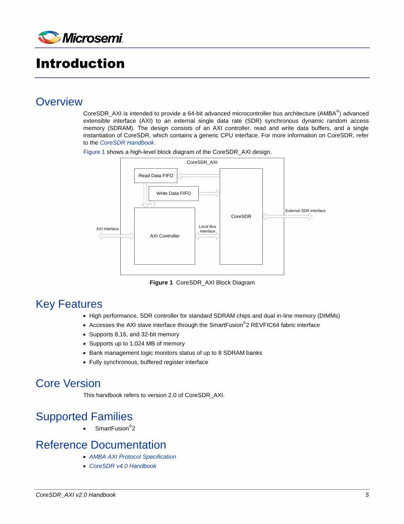
Overview CoreSDR_AXI is intended to provide a 64-bit advanced microcontroller bus architecture (AMBA
®) advanced
extensible interface (AXI) to an external single data rate (SDR) synchronous dynamic random access
memory (SDRAM). The design consists of an AXI controller, read and write data buffers, and a single
instantiation of CoreSDR, which contains a generic CPU interface. For more information on CoreSDR, refer
to the CoreSDR Handbook.
Figure 1 shows a high-level block diagram of the CoreSDR_AXI design.
CoreSDR
CoreSDR_AXI
AXI Controller
Local Bus
Interface
External SDR interface
AXI interface
Read Data FIFO
Write Data FIFO
Figure 1 CoreSDR_AXI Block Diagram
Key Features High performance, SDR controller for standard SDRAM chips and dual in-line memory (DIMMs)
Accesses the AXI slave interface through the SmartFusion®2 REVFIC64 fabric interface
Supports 8,16, and 32-bit memory
Supports up to 1,024 MB of memory
Bank management logic monitors status of up to 8 SDRAM banks
Fully synchronous, buffered register interface
Core Version This handbook refers to version 2.0 of CoreSDR_AXI.
Supported Families SmartFusion
®2
Reference Documentation AMBA AXI Protocol Specification
CoreSDR v4.0 Handbook


CoreSDR_AXI v2.0 Handbook 7
Interface
Parameters / Generics Table 1 outlines the parameters for CORESDR_AXI.
Table 1 ·The Parameters for CoreSDR_AXI
Parameter Default Valid Values Description
Core Parameters
SDRAM_CHIPS 1 1 to 8 Number of chip selects
SDRAM_COLBITS 8 8 to 12 Number of SDRAM column bits
SDRAM_ROWBITS 11 11 to 14 Number of SDRAM row bits
SDRAM_CHIPBITS 3 1 to 3 Number of encoded chip select bits
SDRAM_BANKSTAT
MODULES
4 4, 8 Number of bank status modules
DQ_SIZE 32 8,16,32,64 Width of the SDRAM data bus (DQ). This determines the byte
mapping of AXI to SDR. Need elaboration here, but this is
more of a Phase1 process.
FAMILY 19 19 SmartFusion2
Timing Parameters
RAS 6 1-10 SDRAM active to precharge timing, specified in clock cycles
RCD 3 2-5 SDRAM active to read or write delay, specified in clock cycles
RRD 2 2-3 SDRAM active bank a to active bank b, specified in clock
cycles
RP 3 1-4 SDRAM precharge command period, specified in clock cycles
RC 8 3-12 SDRAM active to active/auto-refresh command period,
specified in clock cycles
RFC 9 2-14 Auto-refresh to active/auto-refresh command period,
specified in clock cycles
MRD 2 1-7 SDRAM load mode register command to active or refresh
command, specified in clock cycles
CL 2 1-4 SDRAM CAS latency, specified in clock cycles
WR 2 1-3 SDRAM write recovery time
Interface
8 CoreSDR_AXI v2.0 Handbook
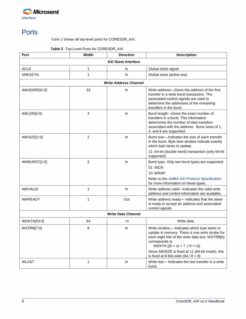
Ports Table 2 shows all top-level ports for CORESDR_AXI.
Table 2 ·Top-Level Ports for CORESDR_AXI
Port Width Direction Description
AXI Slave Interface
ACLK 1 In Global clock signal
ARESETN 1 In Global reset (active low)
Write Address Channel
AWADDR[31:0] 32 In Write address—Gives the address of the first
transfer in a write burst transaction. The
associated control signals are used to
determine the addresses of the remaining
transfers in the burst.
AWLEN[3:0] 4 In Burst length—Gives the exact number of
transfers in a burst. This information
determines the number of data transfers
associated with the address. Burst sizes of 1,
4, and 8 are supported.
AWSIZE[1:0] 2 In Burst size—Indicates the size of each transfer
in the burst. Byte lane strobes indicate exactly
which byte lanes to update.
11: 64-bit (double word) transaction (only 64-bit
supported)
AWBURST[1:0] 2 In Burst type. Only two burst types are supported:
01: INCR
10: WRAP
Refer to the AMBA AXI Protocol Specification
for more information on these types.
AWVALID 1 In Write address valid—Indicates the valid write
address and control information are available.
AWREADY 1 Out Write address ready— Indicates that the slave
is ready to accept an address and associated
control signals.
Write Data Channel
WDATA[63:0] 64 In Write data
WSTRB[7:0] 8 In Write strobes— Indicates which byte lanes to
update in memory. There is one write strobe for
each eight bits of the write data bus. WSTRB[n]
corresponds to
WDATA [(8 × n) + 7 :( 8 × n)].
Since AWSIZE is fixed at 11 (64-bit mode), this
is fixed at 8 bits wide (64 / 8 = 8)
WLAST 1 In Write last— Indicates the last transfer in a write
burst.

CoreSDR_AXI v2.0 Handbook
CoreSDR_AXI v2.0 Handbook 9
Port Width Direction Description
WVALID 1 In Write valid— Indicates that valid write data and
strobes are available,
1: Write data and strobes available
0: Write data and strobes not available
WREADY 1 Out Write ready— Indicates that the slave can
accept the write data:
1: Slave ready
0: Slave not ready
Write Response Channel
BRESP 1 Out Write response— Indicates the status of the
write transaction. The allowable responses are
0: OKAY
1: SLVERR
BVALID 1 Out Write response valid— Indicates that a valid
write response is available:
1: Write response available.
0: Write response not available.
BREADY 1 In Response ready— Indicates that the master
can accept the response information.
1: Master ready
0: Master not ready
Read Address Channel
ARADDR[31:0] 32 In Read address— Gives the initial address of a
read burst transaction. Only the start address
of the burst is provided.
ARLEN[3:0] 4 In Burst length— Gives the exact number of
transfers in a burst. This information
determines the number of data transfers
associated with the address.
ARSIZE[1:0] 2 In Burst size— Indicates the size of each transfer
in the burst.
b00: 8-bit (byte) transaction
b01: 16-bit (half word) transaction
b10: 32-bit (word) transaction
b11:= 64 bit(double word) transaction
Note: Only double word is supported.
ARBURST[1:0] 2 In Burst type— Coupled with the size information,
details how the address for each transfer within
the burst is calculated.
ARVALID 1 In Read address valid— Indicates, when High,
that the read address and control information is
valid
1: Address and control valid
0: Address and control not valid

Interface
10 CoreSDR_AXI v2.0 Handbook
Port Width Direction Description
ARREADY 1 Out Read address ready. This signal indicates that
the slave is ready to accept an address and
associated control signals:
1: Slave ready
0: Slave not ready
Read Data Channel
RDATA[63:0] 64 Out Read data
RRESP 1 Out Read response. This signal indicates the status
of the read transfer. The allowable responses:
0: OKAY
1: SLVERR
RLAST 1 Out Read last. This signal indicates the last transfer
in a read burst.
RVALID 1 Out Read valid. This signal indicates that the
required read data is available and the read
transfer can complete:
1: Read data available
0: Read data not available
RREADY 1 In Read ready. This signal indicates that the
master can accept the read data and response
information:
1: Master ready
0: Master not ready
SDR SDRAM Interface
SDRCLK 1 Out SDRAM clock – Pass-through AXI clock (no
division)
SA[13:0] 14 Out Address bus
BA[1:0] 2 Out Bank address
CS_N[7:0] 8 Out Chip selects
CKE 1 Out Clock enable
RAS_N 1 Out Row address strobe
CAS_N 1 Out Column address strobe
WE_N 1 Out Write enable
DQM[7:0] 8 Out Data mask, byte lane strobes (from WSTRB
above) determine exactly which bytes are
being updated.
8 is the maximum width for this signal. Actual
width is determined by DQ/8. That is, each
byte has its own strobe. For the case of 64-bit
DQ_SIZE, DQM is 8 bits wide.
OE 1 Out Output enable, tristate control for DQ data bus
DQ[DQ_SIZE-1:0] DQ_SIZE Inout Data bus
Note: The Lock, Cache, and Protect features of AXI are not implemented in CoreSDR_AXI.

CoreSDR_AXI v2.0 Handbook 11
Operation
Handshaking AXI uses a READY/VALID handshake. This means that either the master (from the AHB2AXI bridge through
the REVFIC) or the slave (CORESDR_AXI) can delay a transfer. The implication here is that if data is being
read out of CoreSDR, it needs to be stored somewhere, since the local bus interface does not have a
handshaking process. For more information on this, refer to the Overview section on page 5.
Figure 2 shows the AXI handshaking protocol.
When both VALID and READY are asserted, the data is considered as transferred. This applies for both
writes (master controls VALID and slave controls READY) and reads (master controls VALID and slave
control READY).
Figure 2 ·AXI READY with VALID handshake
The implication of handshaking is that the master can hold off a read transaction by indicating that it is not
ready to receive the data by holding the RREADY AXI signal Low. The master can also delay a write
operation by bringing the WVALID signal Low.
This behavior is applied to all the read and write data and address channels. For more information, refer to
the AMBA AXI Protocol Specification.
Timing Diagrams
CoreSDR Local Bus Interface Timing
The following timing diagrams are extracted from the CoreSDR Handbook. For more information on
CoreSDR local bus interface timing, refer to the CoreSDR Handbook.

Operation
12 CoreSDR_AXI v2.0 Handbook
Figure 3 ·CoreSDR Burst Write
Figure 4 ·CoreSDR Burst Read
CoreSDR_AXI v2.0 Handbook
CoreSDR_AXI v2.0 Handbook 13
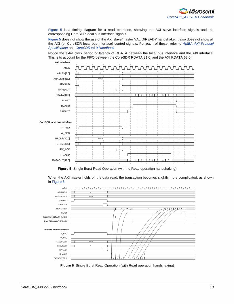
Figure 5 is a timing diagram for a read operation, showing the AXI slave interface signals and the
corresponding CoreSDR local bus interface signals.
Figure 5 does not show the use of the AXI slave/master VALID/READY handshake. It also does not show all
the AXI (or CoreSDR local bus interface) control signals. For each of these, refer to AMBA AXI Protocol
Specification and CoreSDR v4.0 Handbook
Notice the extra clock period of latency of RDATA between the local bus interface and the AXI interface.
This is to account for the FIFO between the CoreSDR RDATA[31:0] and the AXI RDATA[63:0].
2 3 4 5 6 71
AXI interface
ACLK
ARADDR[31:0] ADDR
ARVALID
ARREADY
CoreSDR local bus interface
RDATA[31:0]
RLAST
RVALID
RREADY
ARLEN[3:0] 8
R_REQ
W_REQ
RADDR[30:0] ADDR
8B_SIZE[3:0]
RW_ACK
R_VALID
DATAOUT[31:0] 0
2 3 4 5 6 710
Figure 5 ·Single Burst Read Operation (with no Read operation handshaking)
When the AXI master holds off the data read, the transaction becomes slightly more complicated, as shown
in Figure 6.
2 3 4 5 6 71
ACLK
ARADDR[31:0] ADDR
ARVALID
ARREADY
CoreSDR local bus interface
RDATA[31:0]
RLAST
(from CoreSDRAXI) RVALID
(from AXI master) RREADY
ARLEN[3:0] 8
R_REQ
W_REQ
RADDR[30:0] ADDR
8B_SIZE[3:0]
RW_ACK
R_VALID
DATAOUT[31:0] 0
2 3 4 5 6 710
Figure 6 Single Burst Read Operation (with Read operation handshaking)

Operation
14 CoreSDR_AXI v2.0 Handbook
After the first word of data is transmitted back to the AXI master, the master deasserts the RREADY signals,
which indicates to the slave that it is not ready to receive subsequent data. The slave then holds the current
data until the RREADY signal is asserted again. The DATAOUT bus, however, which is located on the
CoreSDR local bus interface, continues to push out data, as long as the R_VALID signal (incidentally, tied to
the AXI RVALID signal) is asserted. This means that a buffer is required on the CoreSDR_AXI side to buffer
from the SDRAM.
Write operations are similar, except the slave has the ability to hold off transfers by deasserting the
WREADY signal.

CoreSDR_AXI v2.0 Handbook 15
Tool Flows
Licensing CoreSDR_AXI requires a register transfer level (RTL) license to be used and instantiated in unobfuscated
(RTL) mode. Complete source code and a testbench are provided for the core in this release. To generate
an obfuscated RTL, a license is not required, and an unobfuscated testbench is still provided in this release.
SmartDesign CoreSDR_AXI is available for download to the Libero
® System-on-Chip (SoC) IP Catalog through the web
repository. Once it is listed on the catalog, the core can be instantiated using the SmartDesign flow. The
core can be configured using the configuration GUI within SmartDesign.
For information on using SmartDesign to instantiate and generate cores, refer to the Using DirectCore in
Libero SoC User's Guide.
Simulation Flows The User Testbench for CoreSDR_AXI is included in the release.
To run simulations, select the User Testbench flow within SmartDesign and click Save & Generate on the
Generate pane. The User Testbench is selected through the Core Configuration GUI.
When SmartDesign generates the Libero SoC project, it installs the User Testbench files.
User Testbench
The User Testbench provides examples of how to use CoreSDR_AXI with a memory model, which is
provided. The testbench can be modified to suit the requirements.
The testbench consists of an AXI master model, the design under test (CoreSDR_AXI), and a model for a
16-bit mobile SDR memory device.
Synthesis in Libero SoC Having set the design route appropriately, click Synthesis in Libero SoC. The Synthesis window appears,
displaying the Synplicity® project. Set Synplicity to use the Verilog 2001 standard if verilog is being used. To
run Synthesis, select Run.
Place-and-Route in Libero SoC Having set the design route appropriately and run Synthesis, click Layout in the Libero SoC to invoke
Designer. CoreSDR_AXI requires no special place-and-route settings.
.


CoreSDR_AXI v2.0 Handbook 17
SARS Being Resolved
There are no SARS being resolved for CoreSDR_AXI. This is a new core. However, the latest version of
CoreSDR is used as a basis, with any relevant SARs being closed for CoreSDR IP.
Any RTL changes made for CoreSDR_AXI must be implemented in CoreSDR in the future release (4.1).
Table 3 lists the relevant outstanding SARs for CoreSDR.
Table 3 ·CoreSDR SARs To Be Resolved
SAR Type Description
21832 RTL Signals in fastinit.vhd missing drivers. Need to tie-off, remove, or connect, as required
25196 RTL VHDL does not match up with the verilog—parameters are not propagated through the core to
lower-level components (fastsdram block).


CoreSDR_AXI v2.0 Handbook 19
Product Support
Microsemi SoC Products Group backs its products with various support services, including Customer
Service, Customer Technical Support Center, a website, electronic mail, and worldwide sales offices. This
appendix contains information about contacting Microsemi SoC Products Group and using these support
services.
Customer Service Contact Customer Service for non-technical product support, such as product pricing, product upgrades,
update information, order status, and authorization.
From North America, call 800.262.1060 From the rest of the world, call 650.318.4460 Fax, from anywhere in the world 650. 318.8044
Customer Technical Support Center Microsemi SoC Products Group staffs its Customer Technical Support Center with highly skilled engineers
who can help answer your hardware, software, and design questions about Microsemi SoC Products. The
Customer Technical Support Center spends a great deal of time creating application notes, answers to
common design cycle questions, documentation of known issues and various FAQs. So, before you contact
us, please visit our online resources. It is very likely we have already answered your questions.
Technical Support Visit the Microsemi SoC Products Group Customer Support website for more information and support
(http://www.microsemi.com/soc/support/search/default.aspx). Many answers available on the searchable
web resource include diagrams, illustrations, and links to other resources on website.
Website You can browse a variety of technical and non-technical information on the Microsemi SoC Products Group
home page, at http://www.microsemi.com/soc/.
Contacting the Customer Technical Support Center Highly skilled engineers staff the Technical Support Center. The Technical Support Center can be contacted
by email or through the Microsemi SoC Products Group website.
You can communicate your technical questions to our email address and receive answers back by email,
fax, or phone. Also, if you have design problems, you can email your design files to receive assistance. We
constantly monitor the email account throughout the day. When sending your request to us, please be sure
to include your full name, company name, and your contact information for efficient processing of your
request.
The technical support email address is [email protected].
My Cases
Microsemi SoC Products Group customers may submit and track technical cases online by going to My
Cases.

Product Support
20 CoreSDR_AXI v2.0 Handbook
Outside the U.S.
Customers needing assistance outside the US time zones can either contact technical support via email
([email protected]) or contact a local sales office. Sales office listings can be found at
www.microsemi.com/soc/company/contact/default.aspx.
ITAR Technical Support For technical support on RH and RT FPGAs that are regulated by International Traffic in Arms Regulations
(ITAR), contact us via [email protected]. Alternatively, within My Cases, select Yes in the ITAR
drop-down list. For a complete list of ITAR-regulated Microsemi FPGAs, visit the ITAR web page.


50200398-0/03.13
© 2013 Microsemi Corporation. All rights reserved. Microsemi and the Microsemi logo are trademarks of Microsemi Corporation. All other trademarks and service marks are the property of their respective owners.
Microsemi Corporation (NASDAQ: MSCC) offers a comprehensive portfolio of semiconductor
solutions for: aerospace, defense and security; enterprise and communications; and industrial
and alternative energy markets. Products include high-performance, high-reliability analog and
RF devices, mixed signal and RF integrated circuits, customizable SoCs, FPGAs, and
complete subsystems. Microsemi is headquartered in Aliso Viejo, Calif. Learn more at
www.microsemi.com.
Microsemi Corporate Headquarters One Enterprise, Aliso Viejo CA 92656 USA Within the USA: +1 (949) 380-6100 Sales: +1 (949) 380-6136 Fax: +1 (949) 215-4996