copyright warning &...
TRANSCRIPT

Copyright Warning & Restrictions
The copyright law of the United States (Title 17, United States Code) governs the making of photocopies or other
reproductions of copyrighted material.
Under certain conditions specified in the law, libraries and archives are authorized to furnish a photocopy or other
reproduction. One of these specified conditions is that the photocopy or reproduction is not to be “used for any
purpose other than private study, scholarship, or research.” If a, user makes a request for, or later uses, a photocopy or reproduction for purposes in excess of “fair use” that user
may be liable for copyright infringement,
This institution reserves the right to refuse to accept a copying order if, in its judgment, fulfillment of the order
would involve violation of copyright law.
Please Note: The author retains the copyright while the New Jersey Institute of Technology reserves the right to
distribute this thesis or dissertation
Printing note: If you do not wish to print this page, then select “Pages from: first page # to: last page #” on the print dialog screen

The Van Houten library has removed some of the personal information and all signatures from the approval page and biographical sketches of theses and dissertations in order to protect the identity of NJIT graduates and faculty.
ABSTRACT
GPU IMPLEMENTATION OF BLOCK TRANSFORMS
byBoyan Zhang
Traditionally, intensive floating-point computational ability of Graphics Processing Units
(GPUs) has been mainly limited for rendering and visualization application by architec-
ture and programming model. However, with increasing programmability and architecture
progress, GPUs inherent massively parallel computational ability have become an essential
part of today’s mainstream general purpose (non-graphical) high performance computing
system. It has been widely reported that adapted GPU-based algorithms outperform signif-
icantly their CPU counterpart.
The focus of the thesis is to utilize NVIDIA CUDA GPUs to implement orthogo-
nal transforms such as signal dependent Karhunen-Loeve Transform and signal indepen-
dent Discrete Cosine Transform. GPU architecture and programming model are examined.
Mathematical preliminaries of orthogonal transform, eigen-analysis and algorithms are re-
visited. Due to highly parallel structure, GPUs are well suited to such computation. Further,
the thesis examines multiple implementations schemes and configuration, measurement of
performance is provided. A real time processing display application frame is developed to
visually exhibit GPU compute capability.

GPU IMPLEMENTATION OF BLOCK TRANSFORMS
byBoyan Zhang
A ThesisSubmitted to the Faculty of
New Jersey Institute of Technologyin Partial Fulfillment of the Requirements for the Degree of
Master of Science in Electrical Engineering
Department of Electrical and Computer Engineering
June 2012

Copyright ©

APPROVAL PAGE
GPU IMPLEMENTATION OF BLOCK TRANSFORMS
Boyan Zhang
Dr. Ali N Akansu, Thesis Advisor DateProfessor of Electrical and Computer Engineering, NJIT
Dr. Richard Haddad, Committee Member DateProfessor of Electrical and Computer Engineering, NJIT
Dr. Edip Niver, Committee Member DateProfessor of Electrical and Computer Engineering, NJIT
BIOGRAPHICAL SKETCH
Author: Boyan Zhang
Degree: Master of Science
Date: August 2012
Undergraduate and Graduate Education:
• Master of Science in Electrical Engineering,New Jersey Institute of Technology, Newark, New Jersey, 2012
• Bachelor of Science in Electrical Engineering and Underwater Acoustics,Harbin Engineering University, Harbin, Heilongjiang, 2009
Major: Electrical Engineering
iv

To my family,
for their endless love and support
v

ACKNOWLEDGMENT
First and foremost, I would like to express my sincere gratitude to my advisor, Professor
Ali, Akansu, for the opportunity to work under his guidance and for all his support, encour-
agement throughout my study. Professor Akansu not only provided valuable resources but
also shares me with his countless ideas and vision.
I would also like to thank Dr. Richard Haddad. His great teaching in my coursework
really formed the basis for my efforts in this research area. Besides my advisors, I am
heartily grateful to Dr. Edip Niver for serving as members of my thesis committee.
I am also grateful to Mustafa Ugur Torun, Onur Yilmaz, Yanjia Sun and all other
members of laboratory of high performance digital signal processing for sharing their vast
knowledge and valuable life experience with me.
Last but certainly not the least, I would like to express my appreciation to my par-
ents who inspire me pursuing engineering for their constant loving support. My thanks also
go to my friends who provide me various perspectives.
vi
TABLE OF CONTENTS
Chapter Page
1 INTRODUCTION . . . . . . . . . . . . . . . . . . . . . . . . . . . . . . . . . 1
1.1 Objective . . . . . . . . . . . . . . . . . . . . . . . . . . . . . . . . . . . 1
1.2 The Scope of Thesis . . . . . . . . . . . . . . . . . . . . . . . . . . . . . . 2
2 BLOCK ORTHOGONAL TRANSFORM . . . . . . . . . . . . . . . . . . . . . 3
2.1 Vector Spaces and Signal Representation . . . . . . . . . . . . . . . . . . . 3
2.2 Orthogonal Signal Space and Orthogonal Transform . . . . . . . . . . . . . 3
2.3 Why KLT is Optimal Transform . . . . . . . . . . . . . . . . . . . . . . . 6
2.3.1 Correlation and Covariance . . . . . . . . . . . . . . . . . . . . . . 6
2.4 Two-Dimensional Orthogonal Transform . . . . . . . . . . . . . . . . . . . 9
3 CUDA PROGRAMMING MODEL . . . . . . . . . . . . . . . . . . . . . . . . 12
3.1 Introduction to CUDA . . . . . . . . . . . . . . . . . . . . . . . . . . . . . 12
3.2 Hardware Model . . . . . . . . . . . . . . . . . . . . . . . . . . . . . . . 12
3.3 Programming Model . . . . . . . . . . . . . . . . . . . . . . . . . . . . . 13
3.3.1 CUDA Thread Organization . . . . . . . . . . . . . . . . . . . . . 13
3.4 Execution Model . . . . . . . . . . . . . . . . . . . . . . . . . . . . . . . 15
3.5 CUDA Memory Model . . . . . . . . . . . . . . . . . . . . . . . . . . . . 16
3.6 Hardware Perspective . . . . . . . . . . . . . . . . . . . . . . . . . . . . . 17
3.6.1 Dynamic Partitioning of SM Resources . . . . . . . . . . . . . . . 18
4 GPU IMPLEMENTATION . . . . . . . . . . . . . . . . . . . . . . . . . . . . . 19
4.1 Implementing DCT by Definition . . . . . . . . . . . . . . . . . . . . . . . 19
4.2 Implementation Scheme1 . . . . . . . . . . . . . . . . . . . . . . . . . . . 19
4.2.1 Device Data Memory Organization . . . . . . . . . . . . . . . . . . 20
vii
TABLE OF CONTENTS(Continued)
Chapter Page
4.2.2 Scheme1 Kernel Parameter Configuration . . . . . . . . . . . . . . 23
4.3 Implementation Scheme 2 . . . . . . . . . . . . . . . . . . . . . . . . . . . 24
4.4 Implementation Scheme 3 . . . . . . . . . . . . . . . . . . . . . . . . . . . 25
4.5 Tuning Performance and Profiling . . . . . . . . . . . . . . . . . . . . . . 27
4.5.1 Memory Coalescing . . . . . . . . . . . . . . . . . . . . . . . . . . 28
4.5.2 Context Level Analysis . . . . . . . . . . . . . . . . . . . . . . . . 30
4.5.3 Kernel Level Analysis . . . . . . . . . . . . . . . . . . . . . . . . 31
4.5.4 Testing Result Analysis . . . . . . . . . . . . . . . . . . . . . . . . 33
4.6 Eigen Decomposition Implementation . . . . . . . . . . . . . . . . . . . . 33
4.6.1 Jacobi . . . . . . . . . . . . . . . . . . . . . . . . . . . . . . . . . 34
4.6.2 Results and Further Discussion . . . . . . . . . . . . . . . . . . . . 36
4.6.3 Divide and Conquer . . . . . . . . . . . . . . . . . . . . . . . . . . 37
4.6.4 MAGMA Testing Result . . . . . . . . . . . . . . . . . . . . . . . 38
5 REAL TIME DISPLAY APPLICATION FRAME . . . . . . . . . . . . . . . . 39
5.1 Program Flow . . . . . . . . . . . . . . . . . . . . . . . . . . . . . . . . . 39
5.2 FFmpeg . . . . . . . . . . . . . . . . . . . . . . . . . . . . . . . . . . . . 39
5.3 Test Result . . . . . . . . . . . . . . . . . . . . . . . . . . . . . . . . . . . 41
6 CONCLUSION AND FUTURE WORK . . . . . . . . . . . . . . . . . . . . . 44
6.1 Conclusion . . . . . . . . . . . . . . . . . . . . . . . . . . . . . . . . . . 44
6.2 Future Work . . . . . . . . . . . . . . . . . . . . . . . . . . . . . . . . . . 44
APPENDIX A TESTING RESULT FOR IMPLEMENTATION SCHEME 3 . . . . 46
APPENDIX B GPU AND CPU SPECIFICATION . . . . . . . . . . . . . . . . . 49
REFERENCES . . . . . . . . . . . . . . . . . . . . . . . . . . . . . . . . . . . . . 50
viii
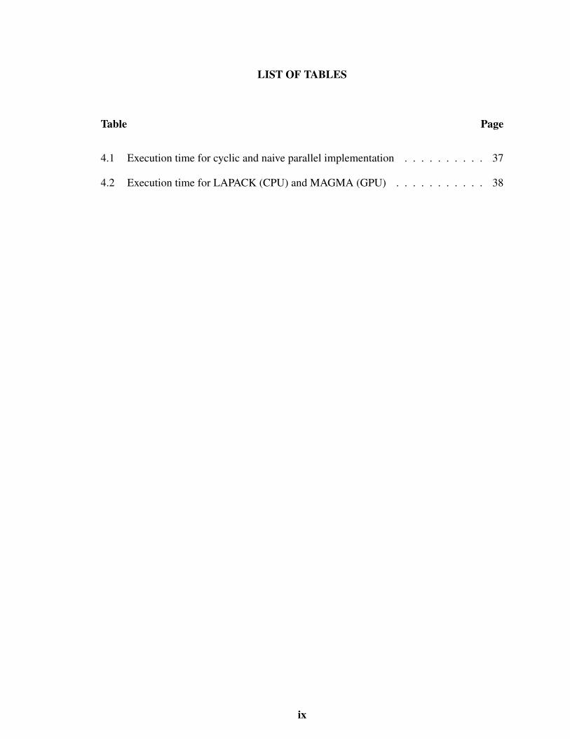
LIST OF TABLES
Table Page
4.1 Execution time for cyclic and naive parallel implementation . . . . . . . . . . 37
4.2 Execution time for LAPACK (CPU) and MAGMA (GPU) . . . . . . . . . . . 38
ix
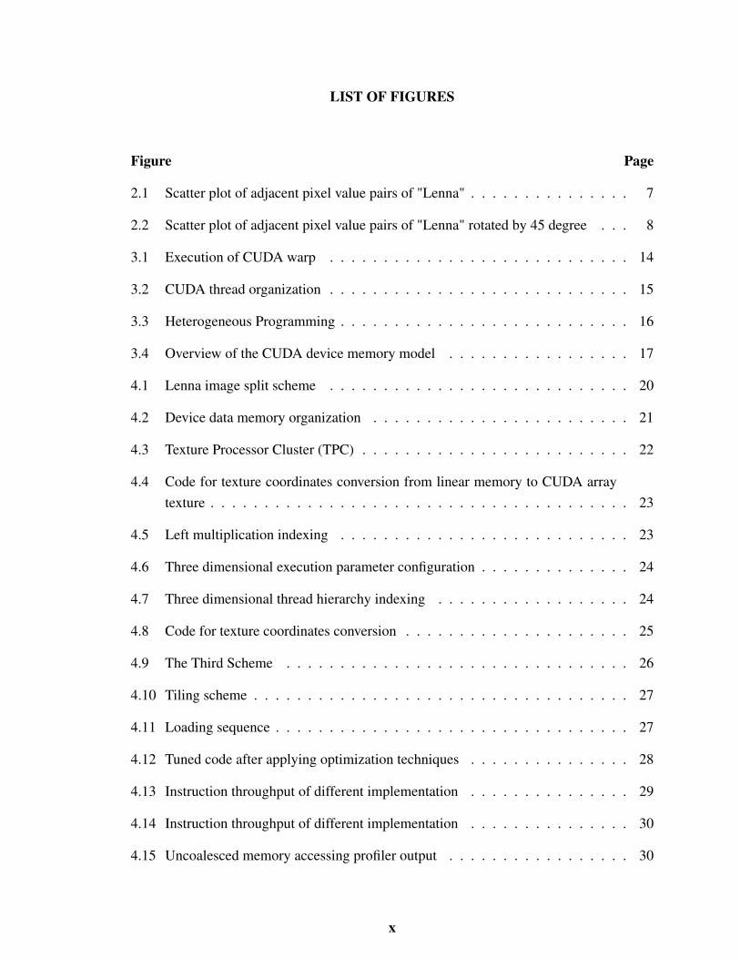
LIST OF FIGURES
Figure Page
2.1 Scatter plot of adjacent pixel value pairs of "Lenna" . . . . . . . . . . . . . . . 7
2.2 Scatter plot of adjacent pixel value pairs of "Lenna" rotated by 45 degree . . . 8
3.1 Execution of CUDA warp . . . . . . . . . . . . . . . . . . . . . . . . . . . . 14
3.2 CUDA thread organization . . . . . . . . . . . . . . . . . . . . . . . . . . . . 15
3.3 Heterogeneous Programming . . . . . . . . . . . . . . . . . . . . . . . . . . . 16
3.4 Overview of the CUDA device memory model . . . . . . . . . . . . . . . . . 17
4.1 Lenna image split scheme . . . . . . . . . . . . . . . . . . . . . . . . . . . . 20
4.2 Device data memory organization . . . . . . . . . . . . . . . . . . . . . . . . 21
4.3 Texture Processor Cluster (TPC) . . . . . . . . . . . . . . . . . . . . . . . . . 22
4.4 Code for texture coordinates conversion from linear memory to CUDA arraytexture . . . . . . . . . . . . . . . . . . . . . . . . . . . . . . . . . . . . . . . 23
4.5 Left multiplication indexing . . . . . . . . . . . . . . . . . . . . . . . . . . . 23
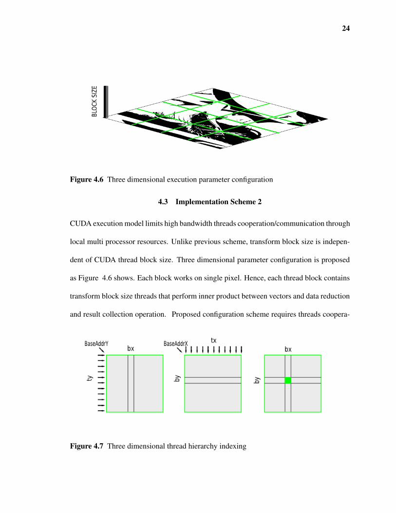
4.6 Three dimensional execution parameter configuration . . . . . . . . . . . . . . 24
4.7 Three dimensional thread hierarchy indexing . . . . . . . . . . . . . . . . . . 24
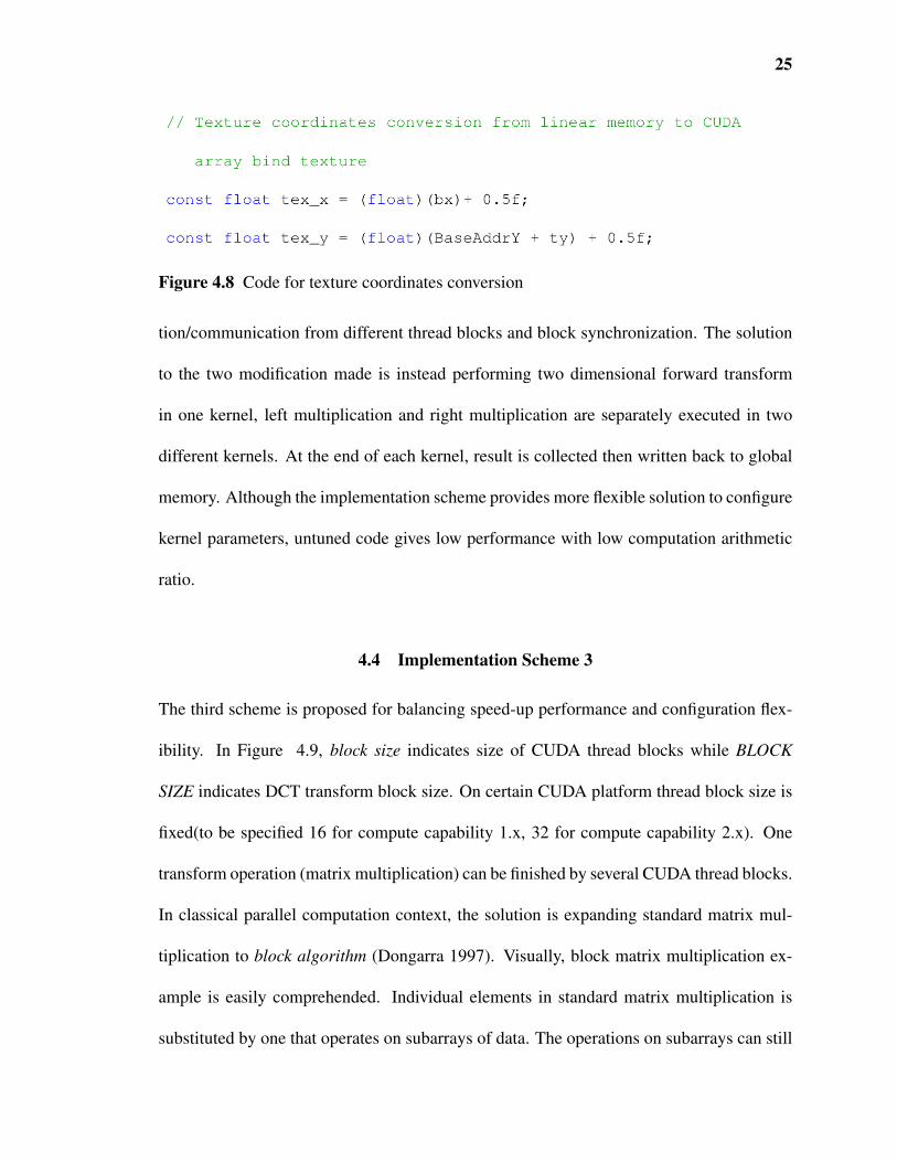
4.8 Code for texture coordinates conversion . . . . . . . . . . . . . . . . . . . . . 25
4.9 The Third Scheme . . . . . . . . . . . . . . . . . . . . . . . . . . . . . . . . 26
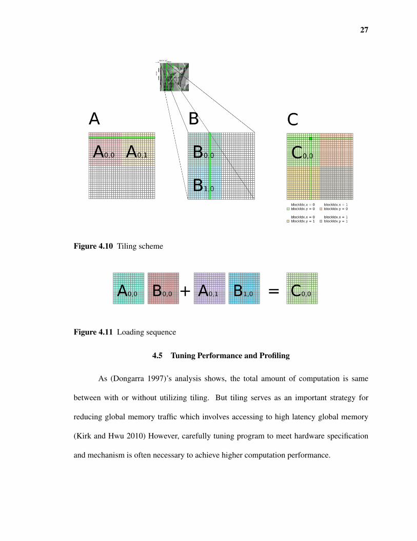
4.10 Tiling scheme . . . . . . . . . . . . . . . . . . . . . . . . . . . . . . . . . . . 27
4.11 Loading sequence . . . . . . . . . . . . . . . . . . . . . . . . . . . . . . . . . 27
4.12 Tuned code after applying optimization techniques . . . . . . . . . . . . . . . 28
4.13 Instruction throughput of different implementation . . . . . . . . . . . . . . . 29
4.14 Instruction throughput of different implementation . . . . . . . . . . . . . . . 30
4.15 Uncoalesced memory accessing profiler output . . . . . . . . . . . . . . . . . 30
x

LIST OF FIGURES(Continued)
Figure Page
4.16 Coalesced memory accessing profiler output . . . . . . . . . . . . . . . . . . . 31
4.17 Profiler output after removing warp serialize . . . . . . . . . . . . . . . . . . . 32
4.18 Summary table for kernel profiler output . . . . . . . . . . . . . . . . . . . . . 32
4.19 Occupancy analysis for kernel with lower efficiency . . . . . . . . . . . . . . . 32
4.20 Occupancy analysis for kernel with higher efficiency . . . . . . . . . . . . . . 32
5.1 OpenGL Display Flow . . . . . . . . . . . . . . . . . . . . . . . . . . . . . . 40
5.2 Display Routine Flow . . . . . . . . . . . . . . . . . . . . . . . . . . . . . . . 41
5.3 Video Data Flow . . . . . . . . . . . . . . . . . . . . . . . . . . . . . . . . . 42
5.4 Image grabbed from raw video input . . . . . . . . . . . . . . . . . . . . . . . 42
5.5 Image grabbed from video after one dimensional DCT transform . . . . . . . . 43
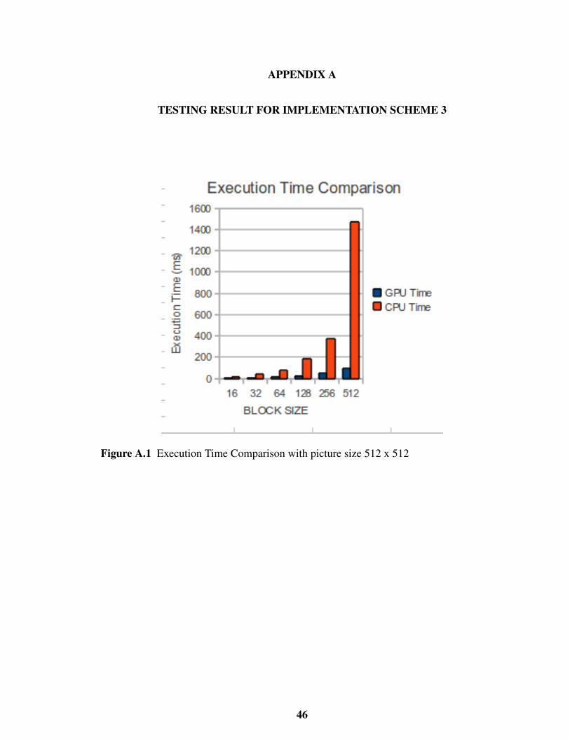
A.1 Execution Time Comparison with picture size 512 x 512 . . . . . . . . . . . . 46
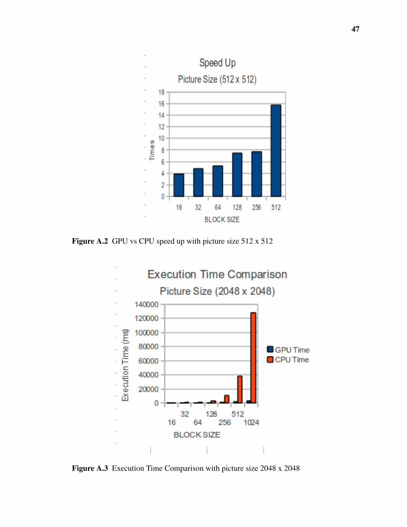
A.2 GPU vs CPU speed up with picture size 512 x 512 . . . . . . . . . . . . . . . 47
A.3 Execution Time Comparison with picture size 2048 x 2048 . . . . . . . . . . . 47
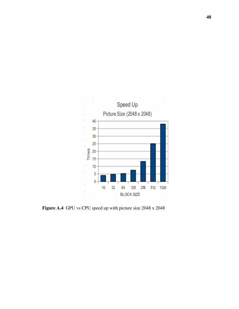
A.4 GPU vs CPU speed up with picture size 2048 x 2048 . . . . . . . . . . . . . . 48
xi
CHAPTER 1
INTRODUCTION
1.1 Objective
Orthogonal transforms decorrelate the signal and repack their energy into less number of
coefficients, which is the purpose of transform coding (Akansu 2000). The thesis aims at
implementation Graphic Processing Unit GPU based block transform that would provide
dramatic increase in computational speed as compared to CPU-based implementation.
Historically, a GPU serves as co-processor to the central processing unit. When it
comes to hardware features. The GPU is designed with a mathematically-intensive, highly
parallel architecture for rendering graphics (Tee 2011).The increased programmability of
the GPUs has opened up the potential to execute non-graphics computation on the GPU or
general purpose computing on GPU (GPGPU) by utilizing the GPU’s massively parallel
architecture with high memory bandwidth.
Two well-known and important orthogonal transforms, Discrete Cosine Transform
or DCT and Karhunen-Loeve Transfrom or KLT are taken as example to be discussed and
implemented. KLT, the unique input-signal dependent with feature of perfect decorrelation
is optimal block transform (Akansu 2000).In essence, KLT is eigen-decomposition prob-
lem. Multiple algorithms, implementation and performance measurement are discussed in
the thesis. DCT is an approach of the KLT, as a reasonable balance of optimality of the
input decorrelation and the computational complexity.
In addition to demonstrating the efficient use of GPU hardware, various implemen-
tation schemes and configuration profiling are presented to show GPU based algorithm
1
2
development work flow of how to achieve high performance by carefully choosing strate-
gies. A real time display application frame is also developed to exhibit potential of utilizing
GPU interoperability in real time signal processing.
1.2 The Scope of Thesis
Chapter 2 introduces concepts of signal representation, theory of block orthogonal trans-
form and discusses KLT as perfect signal decorrelator. Chapter 3 talks about CUDA Pro-
gramming model in both hardware and software perspectives. Chapter 4 presents algo-
rithms design and configuration details of implementation of DCT and KLT. Performance
measurement and profiling result are also provided. Chapter 5 shows real time display
application frame with kernel developed from previous chapters.
CHAPTER 2
BLOCK ORTHOGONAL TRANSFORM
2.1 Vector Spaces and Signal Representation
In context of signal analysis, discrete signal can be represented as a vector xxx = [x1, . . . ,xn]T ,
which will also be considered as a vector in vector space. For the convenience of future
discussion, a N dimensional vector (or signal vector xxx) will always be represented in col-
umn form or transpose of a row vector. A column vector xxx or a row vector xxxT can be written
as an n-tuple with n elements:
xxxT = [x1,x2, . . . ,xN ] xxx =
x1
x2
...
xN
. (2.1)
2.2 Orthogonal Signal Space and Orthogonal Transform
The signal xxx can be considered as a random process, of which each element can be treated
as a random variable with certain probability distribution. In the case of representing a
sequence (discrete-time or discrete variable signal), orthogonal functions, structured as
bases, are used in signal expansions (Akansu 2000). Applying linearly independence of
orthogonal basis, it can be shown that a discrete signal xxx = [x1,x2, . . . ,xN ] can be uniquely
represented as linear combination of orthogonal basis.Here we reference orthogonal matrix
as the object of discussion, for the reason that, through Gram-Schmidt Orthogonalization,
3

4
the corresponding orthonormal matrix of an orthogonal matrix can be obtained. Orthogonal
matrix retains all relevant properties of orthonormal matrix.
Based on discussion above, orthogonal transform can be developed. If an N by N
square matrix AAA is invertible, its inverse matrix AAA−1 equals to its own transpose AAAT , which
is AAA−1 = AAAT . Then an orthogonal transform of a column vector xxx = [x1,x2, . . . ,xN ]T can be
defined as
yyy = AAAxxx (2.2)
or in the expansion form
yyy =
a11 a12 . . . a1N
a21 a22 . . . a2N
......
......
aN1 aN2 . . . aNN
x1
x2
...
xN
(2.3)
If we define aaai = [a1i,a2i, . . . ,aNi] as ith column vector of A, above forward transform can
be rewritten as
yyy =
y1
y2
...
yN
= AAAT x =
aaaT1
aaaT2
...
aaaTN
xxx (2.4)
Where A is transform matrix. Correspondingly, inverse transform can be obtained by left
5
multiplying AAA on both sides of transform equation above,
xxx =
x1
x2
...
xn
= AAAyyy =
[aaa1 aaa2 . . . aaaN
]
y1
y2
...
yN
(2.5)
Above operation relies on the property of orthogonal matrix that transpose of orthogonal
matrix is equal to its inverse (Axler 1997). Hence, AAAAAAT = AAAAAA−1 = III. The bi-direction
transform above also reveals the Parseval Relation between signal domain and transform
domain. The energy in a signal sequence is defined as the square of the norm. Signal energy
is preserved under the transformation and can also be measured by the norm of transformed
(spectral) coefficients (Akansu 2000).
Geometrically, above operation can be interpreted as signal vector xxx represented by
a set of orthonormal basis defined in an N Dimensional space being applied coordinate
rotation defined by orthogonal transform matrix through matrix-vector operation. Trans-
form coefficients can be seen as signal representation with rotated coordinate. Considering
a signal matrix with multiple signal vector entries XXX = [xxx1,xxx2, . . . ,xxxN ]. Through opera-
tion (transform) defined previously, block orthogonal transform is an expansion of matrix-
vector to matrix-matrix case. Let signal be matrix with N by N elements, such a matrix can
be converted to an N2 dimension vector by cascading all the vectors column by column.
Hence, each block can then be interpreted as a vector with length N2 (Fisher 1995).

6
2.3 Why KLT is Optimal Transform
2.3.1 Correlation and Covariance
Let signal vector xxxi be a random variable vector, the covariance matrix of xxx is defined as
CCCx = EEE[(xxx−µµµx)(xxx−µµµx)
T ]= EEE[xxxxxxT ]−µµµxµµµTx =
σ2
0 . . . σ20(N−1)
......
...
σ2(N−1)0 . . . σ2
N−1
(2.6)
where µµµx is the mean vector of random vector xxx, the element σ2i j is the covariance of xi and
x j. Correspondingly, the correlation matrix composed of all correlation coefficients:
RRRx =
r2
0 . . . r20(N−1)
......
...
r2(N−1)0 . . . r2
N−1
(2.7)
where ri j is correlation coefficient between the two variables, defined as the covariance σ2i j
normalized by σi and σ j. It can be assumed that xxx is centred with µµµ = 0 without loss ofgen-
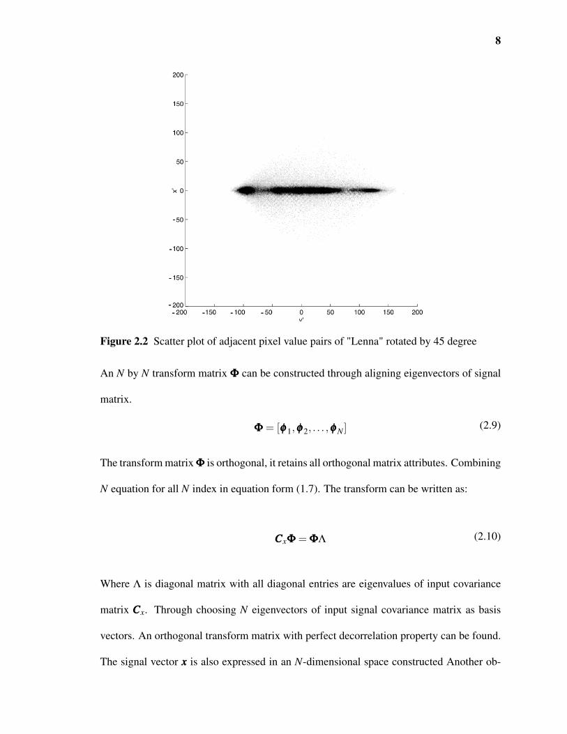
erality. Figure 2.1 and Figure 2.2 gives a perfect illustration of correlation between pixels
in an actual image (Lenna). Each dot represents a pixel in the image with the x coordinate
being its gray level value and the y coordinate being the gray level value of its neighbour
to the right (Rao 2000). The diagonal convergence reveals the strong correlation between
neighbouring pixels. Figure 2.2 (Rao 2000) shows result of 45 degree rotation on input
signal pairs. Simply after 45 degree rotation, the pre-exist correlation between neighbour
pixels have already been significantly reduced. Here, covariance matrix can be introduced

7
Figure 2.1 Scatter plot of adjacent pixel value pairs of "Lenna"
to represent correlation among all pixels. Such correlation between adjunct pixels is re-
flected in first sub-diagonal elements of covariance matrix. Intuitively, all non-diagonal
elements of covariance matrix reflects correlation between any two different spatial image
pixels. From a signal coding standpoint, the purpose of transform coding is to decompose
a batch of correlated signal samples into a set of uncorrelated spectral coefficients (Akansu
2000). If idea of decorrelation spans to the example above, after transform desired covari-
ance matrix of uncorrelated spectral coefficients is a diagonal matrix. The Karhunen-Loeve
transform (KLT) has property to diagonalized input signal covariance matrix.
Suppose λk is kth eigenvalue of the covariance matrix Cx,
λkφk =CCCxφk 1≤ k ≤ N (2.8)
8
Figure 2.2 Scatter plot of adjacent pixel value pairs of "Lenna" rotated by 45 degree
An N by N transform matrix ΦΦΦ can be constructed through aligning eigenvectors of signal
matrix.
ΦΦΦ = [φφφ 1,φφφ 2, . . . ,φφφ N ] (2.9)
The transform matrix ΦΦΦ is orthogonal, it retains all orthogonal matrix attributes. Combining
N equation for all N index in equation form (1.7). The transform can be written as:
CCCxΦΦΦ = ΦΦΦΛ (2.10)
Where Λ is diagonal matrix with all diagonal entries are eigenvalues of input covariance
matrix CCCx. Through choosing N eigenvectors of input signal covariance matrix as basis
vectors. An orthogonal transform matrix with perfect decorrelation property can be found.
The signal vector xxx is also expressed in an N-dimensional space constructed Another ob-

9
servation can be made is the covariance matrix of transform coefficients is same as covari-
ance matrix of input signal vector, which means the spare energy of input signal vector x
contract in first N component after transform. The example reveals that the signal charac-
teristics of local correlation is reflected in the correlation matrix RRRx. All elements along
the main diagonal take the maximum value, representing the maximal self-correlation of
each signal sample, and all off-diagonal elements takes a smaller value representing the
cross-correlation between the two signal samples xi and x j. rrri j close to the main diagonal
tends to take large values than those whiche are farther away from the main diagonal, due
to local correlation.
2.4 Two-Dimensional Orthogonal Transform
Taking KLT as an example, we can extend one-dimensional orthogonal transform to two-
dimensional case, by assuming separable statistics of rows and columns(which is reason-
able by examination of previous image signal example)(Rao 2011), two dimensional real
random input κκκ:
κκκ =
x11 . . . x1N
... . . . ...
xN1 . . . xNN
(2.11)
By rearranging order of κ, (N2×1) column vector u can be obtained:
u = (x11 . . .x1Nx21 . . .x2N . . .xN1xNN)T (2.12)
10
If assuming separable statistics of the row and the column, Here Φ1 and Φ2 are orthogonal
matrices in the KLT matrix Ψ. After 2D separation we have:
Ψ = Φ1⊗Φ2 (2.13)
The symbol ⊗ stands for Kronecker Product of two matrices can be defined as:
A⊗B =
a11B . . . a1nB
... . . . ...
am1B . . . amnB
(2.14)
When A and B matrices are respectively of sizes (m×n) and (p×q). Since Φ1 and Φ2 are
orthogonal, then Ψ is orthogonal. Equation (4) holds,
RΨk = λkΨk (2.15)
Perform KLT to u, we obtain µ: (?)
µ = ΨT u = (ΦT
1 ⊗ΦT2 ) (2.16)
Left Multipying Ψ = (ΨT )−1 on both sides of above equation, 2D case inverse transform
with respect to µ can be shown:
u = Ψµ (2.17)
To generalize procedure above, a row-column operation can be taken. First, one
dimensional orthogonal transform of the signal along the columns, then one dimensional
11
orthogonal transform can be applied along rows. The two-dimensional forward and inverse
transform can be expressed as:
yyy = AAAxxxAAAT (2.18)
xxx = AAAT yyyAAA (2.19)
Although the KLT is optimal among all orthogonal transforms, other orthogonal
transforms are still widely used for two reasons. First, by definition the KLT transform
is for random signals and it depends on the specific data being analysed. The transform
matrix is composed of the eigenvectors of the covariance matrix CCCx of the signal xxx, which
can be estimated only upon data. Second, the computational cost of the KLT transform is
much higher than other orthogonal transforms. Moreover, fast algorithms exist for many
transforms such as DFT, DCT. For these reasons, the DCT may be the preferred method in
many applications. The KLT can be used when the covariance matrix of the data can be
estimated and computational cost is not critical. Also the KLT as the optimal transform can
be used to serve as a standard against which all other transform methods can be compared
and evaluated (Akansu 2000). Although no fast algorithm exists for the KLT, it can be
approximated by DCT if the signal locally correlated As most signals of interest in practice
are likely to be locally correlated we can always expect the results of the DCT transform
are close to the optimal transform of KLT.

CHAPTER 3
CUDA PROGRAMMING MODEL
3.1 Introduction to CUDA
Compute Unified Device Architecture (CUDA) is a general purpose parallel computing ar-
chitecture developed by NVIDIA that leverage the parallel computing ability in NVIDIA
Graphics Processing Units (GPUs) to solve many complex computational problems in a
more efficient way than on a Central Processing Unit (CPU) (NVIDIA 2010). The parallel
computing engine in GPU is accessible to programmers through ′CUDA C′ (industry stan-
dard C with NVIDIA extensions and certain restrictions) (Wik 2010). It transparently scales
its parallelism and inherent floating point processing ability allows that modern GPUs
emerge not only as a specialized graphic processors but also a numerical co-processors
for high performance general application on CPU.
3.2 Hardware Model
In CUDA hardware model. host is often referred as CPU. Device is a GPU connected to
a host through a high speed IO bus slot, typically a PCI-Express (Wolfe 2010). CUDA
device has its own device memory on GPU. Programmed DMA, can operate concurrently
with both host and device can be used to transfer data between host and device memories.
Although CUDA parallelism model shares some features of popular Single Instruc-
tion Multiple Data (SIMD) and Single Program Multiple Data (SPMD) parallel schemes,
it has to be noted that the architecture should not be simply categorised as any one of
the classes. NVIDIA introduced Single Instruction Multiple Thread (SIMT) architecture
12

13
which combines features of multiple parallel models. Similar to SIMD vector organiza-
tions that a single instruction controls multiple processing elements, in instruction and
data level, threads are organised in groups (warps) that execute same instruction simul-
taneously (NVIDIA 2010). However, unlike popular SIMD architecture implementation
Streaming SIMD Extension (SSE) on CPU, each CUDA thread has private register, which
allows parallel threads process multiple data elements from different address without being
packed in single register. The mechanism change–without extra alignment instructions re-
quired, directly affects programming behaviour (Kirk and Hwu 2010). On the other hand,
thread block executes independently, within thread block private shared memory block
being used for thread cooperation and communication. But synchronization and communi-
cation among blocks is limited.
3.3 Programming Model
3.3.1 CUDA Thread Organization
CUDA thread hierarchy is organized into a 3 level hierarchy. The basic parallel unit is
warp, which also defines hardware memory bandwidth of GPU device. Each warp has
total 32 threads, when actual execution, each warp is divided into two half warps and
scheduled to execution queue by hardware scheduler (Figure 3.1) (Stein 2010). From
programmer point of view, CUDA language extension does not provide explicit definition
to control warp behaviour flow explicitly. Hence, the thread blocks can be seen at the
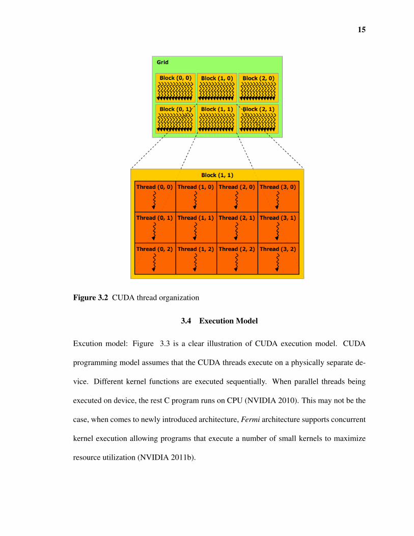
bottom of programmable CUDA thread structure as Figure 3.2 shows. Grid is a collection
of thread blocks and it can be seen as an acronym of device. For the reason that, in current
architecture, only one grid on device at a time is allowed when the kernel being launched
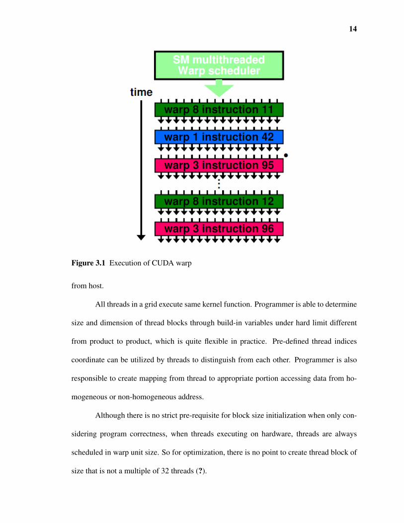
14
Figure 3.1 Execution of CUDA warp
from host.
All threads in a grid execute same kernel function. Programmer is able to determine
size and dimension of thread blocks through build-in variables under hard limit different
from product to product, which is quite flexible in practice. Pre-defined thread indices
coordinate can be utilized by threads to distinguish from each other. Programmer is also
responsible to create mapping from thread to appropriate portion accessing data from ho-
mogeneous or non-homogeneous address.
Although there is no strict pre-requisite for block size initialization when only con-
sidering program correctness, when threads executing on hardware, threads are always
scheduled in warp unit size. So for optimization, there is no point to create thread block of
size that is not a multiple of 32 threads (?).
15
Figure 3.2 CUDA thread organization
3.4 Execution Model
Excution model: Figure 3.3 is a clear illustration of CUDA execution model. CUDA
programming model assumes that the CUDA threads execute on a physically separate de-
vice. Different kernel functions are executed sequentially. When parallel threads being
executed on device, the rest C program runs on CPU (NVIDIA 2010). This may not be the
case, when comes to newly introduced architecture, Fermi architecture supports concurrent
kernel execution allowing programs that execute a number of small kernels to maximize
resource utilization (NVIDIA 2011b).
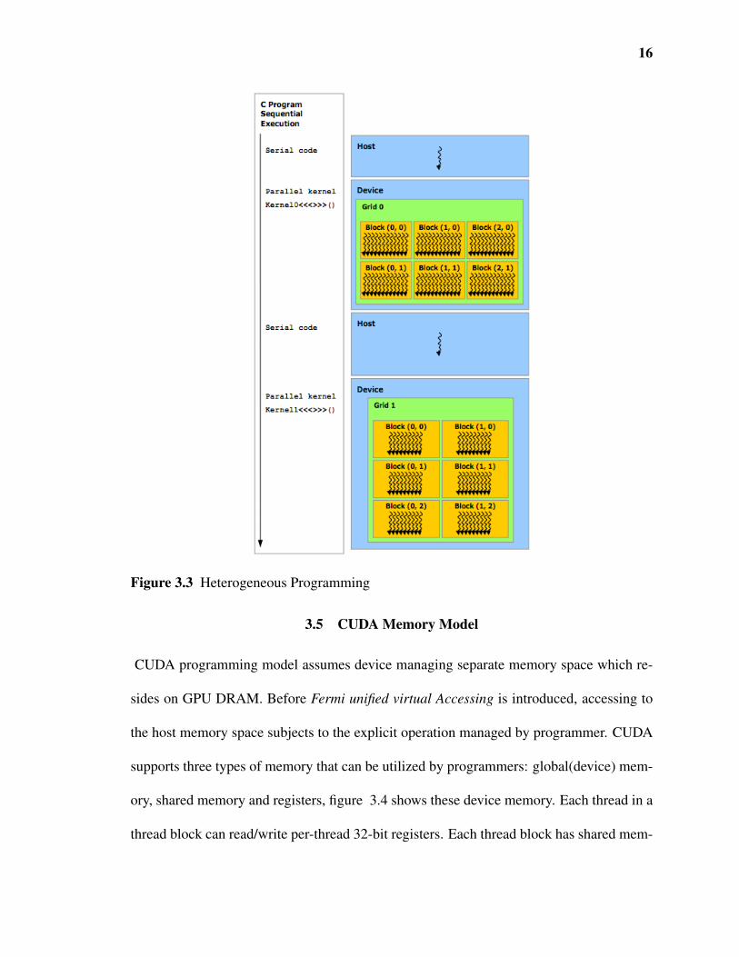
16
Figure 3.3 Heterogeneous Programming
3.5 CUDA Memory Model
CUDA programming model assumes device managing separate memory space which re-
sides on GPU DRAM. Before Fermi unified virtual Accessing is introduced, accessing to
the host memory space subjects to the explicit operation managed by programmer. CUDA
supports three types of memory that can be utilized by programmers: global(device) mem-
ory, shared memory and registers, figure 3.4 shows these device memory. Each thread in a
thread block can read/write per-thread 32-bit registers. Each thread block has shared mem-

17
Figure 3.4 Overview of the CUDA device memory model
ory visible to all threads within the block and with the same lifetime as the block (NVIDIA
2010). Registers and shared memory are on-chip memories. Variables that reside in these
types can be accessed at very high speed (it takes about 20 clock cycles) in a highly parallel
manner. Shared memory is an efficient mean for threads to cooperate by sharing input data
and the intermediate results of processed data (Kirk and Hwu 2010). Appropriate accessing
may have shared memory works as fast as registers. All threads have access to the same
global memory. Several hundred clock cycles are needed to access data in device memory.
As part of of device memory, constant and texture memory reside off-chip. However, con-
stant memory is read-only and cached, it supports short-latency, high-bandwidth memory
access by device all threads access the same location simultaneously (Kirk and Hwu 2010).
3.6 Hardware Perspective
It is important to understand the aforementioned scalability and limiting factor on program-
ming side. Such Scalability roots in hardware as previous shown, the structure of GPU
18
building blocks is self similar. The threads of a thread block execute concurrently on one
multiprocessor, and multi thread blocks can execute concurrently on one multiprocessor
(NVIDIA 2010). Consequently, streaming multiprocessors (SMs) can be seen as hardware
abstraction basic unit of CUDA architecture. As its name suggests, each streaming multi-
processors contains multiple stream processors(SPs). Control logic and instruction cache
is shared between different SPs.
3.6.1 Dynamic Partitioning of SM Resources
Because of all threads in a thread block execute on an SM, GPU hardware designers are
able to provide low-latency local on-chip memory inside SMs to reduce external memory
bandwidth requirement. This is an elegant solution for avoiding known scaling issues with
maintaining coherent caches in multi core processors. Including more higher performance
components in next generation enables forward compatible. Functional behaviour is identi-
cal across the scaling range; one application will run unchanged on any implementation of
an architecture family (Kirk and Hwu 2010). To programmers, the most visible difference
between various CUDA products is "scale" of resource– size and dimension of threads and
thread blocks supported.
The execution resources such as memory usage, threads, threads block distribution
are dynamically partitioned and assigned on SMs. This mechanism makes the SMs versa-
tile. They can either execute many thread blocks with few threads inside, or execute fewer
number blocks, each of which consists of many threads (Kirk and Hwu 2010). However,
this can result in underutilizing or overutilizing SM resources which may affect application
performance.

CHAPTER 4
GPU IMPLEMENTATION
4.1 Implementing DCT by Definition
This solution is never used in practice when calculating block by block DCT transform
on CPU because its high computational complexity relatively to some "separable meth-
ods". However such implementation matches/maps nicely to CUDA programming model,
architecture, which could be used to exhibit GPU computational capability.
From previous shown 2D separable transform property, 2D separable forward DCT
can be expressed in the following form in matrix notation:
YYY = AAA XXX AAAT (4.1)
Furthermore, above operation can be dissected to two separate matrix multiplications AAAXXX
and (AAAXXX)AAAT .
4.2 Implementation Scheme1
One of the primary concern of correctly implementation algorithm on CUDA is how to
create proper mapping from parallel executing threads to data address. Definition for clar-
ify, to avoid confusion, some notations need to be introduced. N by N block of pixels will
be further referred as simply block or pixel blocks. CUDA threads grouped into execution
block will be referred to as CUDA-block or CUDA-thread block.
The most direct thread mapping scheme is one to one mapping from thread to pixel
19
20
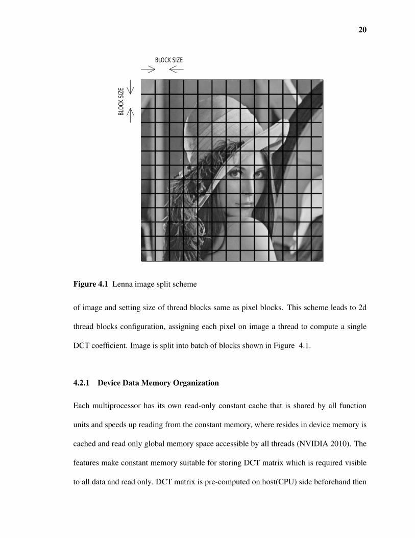
Figure 4.1 Lenna image split scheme
of image and setting size of thread blocks same as pixel blocks. This scheme leads to 2d
thread blocks configuration, assigning each pixel on image a thread to compute a single
DCT coefficient. Image is split into batch of blocks shown in Figure 4.1.
4.2.1 Device Data Memory Organization
Each multiprocessor has its own read-only constant cache that is shared by all function
units and speeds up reading from the constant memory, where resides in device memory is
cached and read only global memory space accessible by all threads (NVIDIA 2010). The
features make constant memory suitable for storing DCT matrix which is required visible
to all data and read only. DCT matrix is pre-computed on host(CPU) side beforehand then
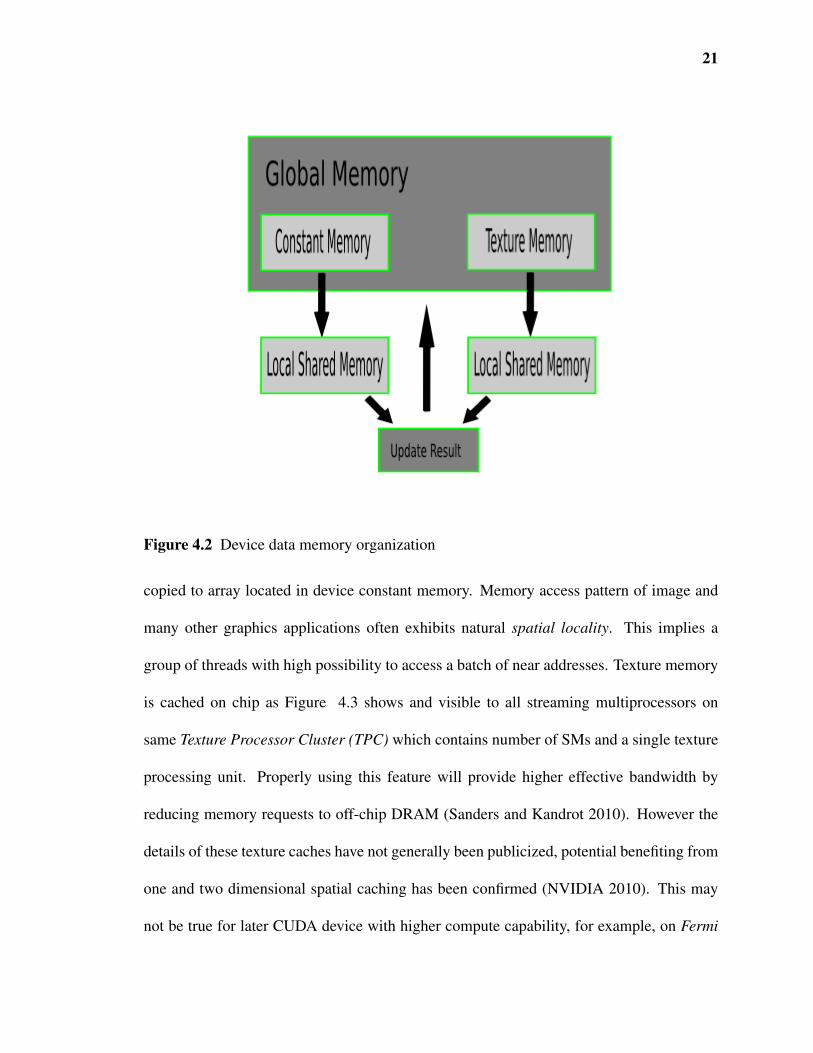
21
Figure 4.2 Device data memory organization
copied to array located in device constant memory. Memory access pattern of image and
many other graphics applications often exhibits natural spatial locality. This implies a
group of threads with high possibility to access a batch of near addresses. Texture memory
is cached on chip as Figure 4.3 shows and visible to all streaming multiprocessors on
same Texture Processor Cluster (TPC) which contains number of SMs and a single texture
processing unit. Properly using this feature will provide higher effective bandwidth by
reducing memory requests to off-chip DRAM (Sanders and Kandrot 2010). However the
details of these texture caches have not generally been publicized, potential benefiting from
one and two dimensional spatial caching has been confirmed (NVIDIA 2010). This may
not be true for later CUDA device with higher compute capability, for example, on Fermi

22
Figure 4.3 Texture Processor Cluster (TPC)
architecture device, global memory accessing is also L1 cached (NVIDIA 2011b).
Each thread loads correspond one pixel data from texture memory to shared mem-
ory. Bitwise left shift operation is used for early generation of CUDA hardware perfor-
mance optimization, which had considerably slower integer arithmetic performance than
floating point. When transform block size is not exponential of 2, bitwise operation will be
substituted by intrinsic float multiplication function (NVIDIA 2010). To ensure the whole
block is loaded, all threads are aligned at synchronization barrier. The thread computes
inner product between two vectors. To perform correct inner product between ΦT and X ,
indexing strategy is adjusted as Figure 4.5 shows. Synchronization barrier is also utilized
to ensure left multiplication across all thread blocks has been performed. Right multiplica-
tion between intermediate result and DCT coefficients follows similar manner mentioned
above (without transpose involved). After all elements in block being updated, local result
is copied back to the destination in global memory.
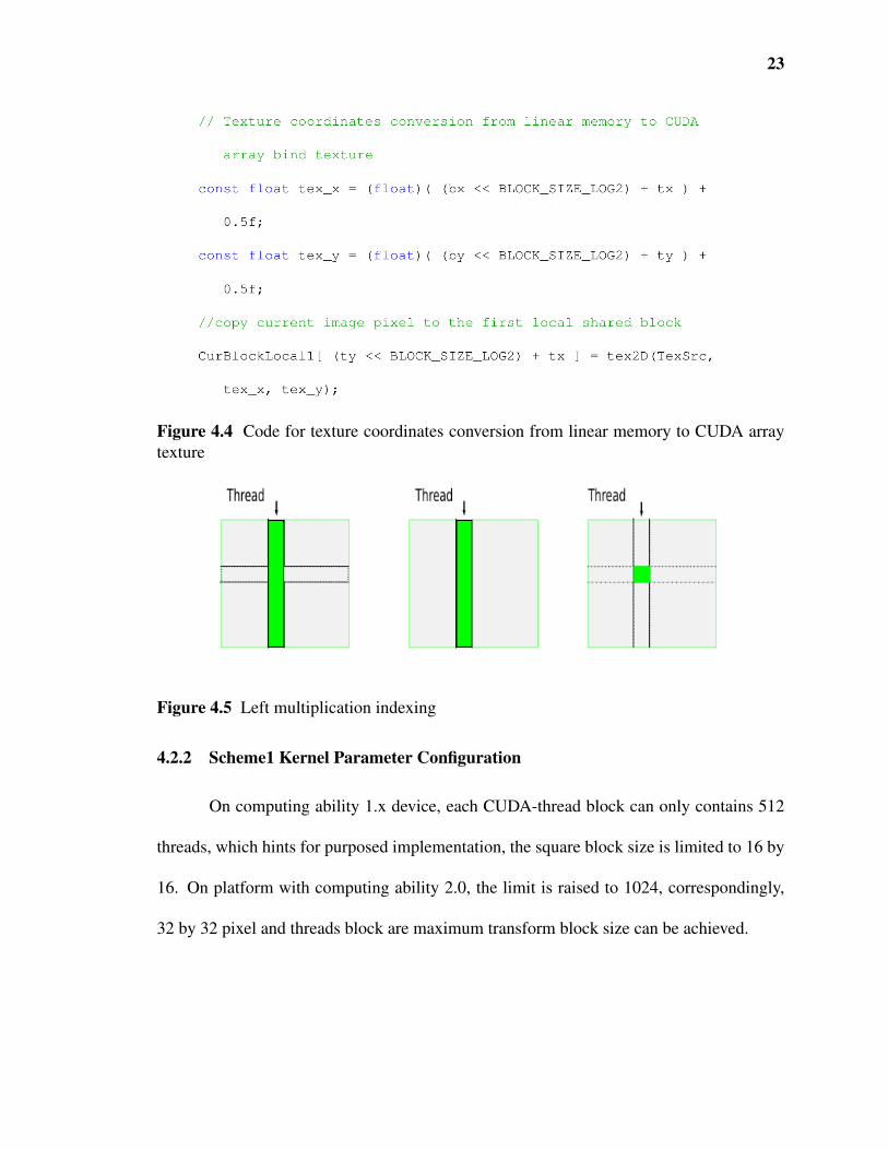
23
Figure 4.4 Code for texture coordinates conversion from linear memory to CUDA arraytexture
Figure 4.5 Left multiplication indexing
4.2.2 Scheme1 Kernel Parameter Configuration
On computing ability 1.x device, each CUDA-thread block can only contains 512
threads, which hints for purposed implementation, the square block size is limited to 16 by
16. On platform with computing ability 2.0, the limit is raised to 1024, correspondingly,
32 by 32 pixel and threads block are maximum transform block size can be achieved.
24
Figure 4.6 Three dimensional execution parameter configuration
4.3 Implementation Scheme 2
CUDA execution model limits high bandwidth threads cooperation/communication through
local multi processor resources. Unlike previous scheme, transform block size is indepen-
dent of CUDA thread block size. Three dimensional parameter configuration is proposed
as Figure 4.6 shows. Each block works on single pixel. Hence, each thread block contains
transform block size threads that perform inner product between vectors and data reduction
and result collection operation. Proposed configuration scheme requires threads coopera-
Figure 4.7 Three dimensional thread hierarchy indexing
25
Figure 4.8 Code for texture coordinates conversion
tion/communication from different thread blocks and block synchronization. The solution
to the two modification made is instead performing two dimensional forward transform
in one kernel, left multiplication and right multiplication are separately executed in two
different kernels. At the end of each kernel, result is collected then written back to global
memory. Although the implementation scheme provides more flexible solution to configure
kernel parameters, untuned code gives low performance with low computation arithmetic
ratio.
4.4 Implementation Scheme 3
The third scheme is proposed for balancing speed-up performance and configuration flex-
ibility. In Figure 4.9, block size indicates size of CUDA thread blocks while BLOCK
SIZE indicates DCT transform block size. On certain CUDA platform thread block size is
fixed(to be specified 16 for compute capability 1.x, 32 for compute capability 2.x). One
transform operation (matrix multiplication) can be finished by several CUDA thread blocks.
In classical parallel computation context, the solution is expanding standard matrix mul-
tiplication to block algorithm (Dongarra 1997). Visually, block matrix multiplication ex-
ample is easily comprehended. Individual elements in standard matrix multiplication is
substituted by one that operates on subarrays of data. The operations on subarrays can still
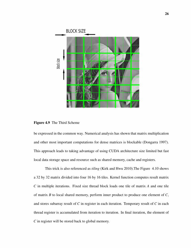
26
Figure 4.9 The Third Scheme
be expressed in the common way. Numerical analysis has shown that matrix multiplication
and other most important computations for dense matrices is blockable (Dongarra 1997).
This approach leads to taking advantage of using CUDA architecture size limited but fast
local data storage space and resource such as shared memory, cache and registers.
This trick is also referenced as tiling (Kirk and Hwu 2010).The Figure 4.10 shows
a 32 by 32 matrix divided into four 16 by 16 tiles. Kernel function computes result matrix
C in multiple iterations. Fixed size thread block loads one tile of matrix A and one tile
of matrix B to local shared memory, perform inner product to produce one element of C,
and stores subarray result of C in register in each iteration. Temporary result of C in each
thread register is accumulated from iteration to iteration. In final iteration, the element of
C in register will be stored back to global memory.
27
Figure 4.10 Tiling scheme
Figure 4.11 Loading sequence
4.5 Tuning Performance and Profiling
As (Dongarra 1997)’s analysis shows, the total amount of computation is same
between with or without utilizing tiling. But tiling serves as an important strategy for
reducing global memory traffic which involves accessing to high latency global memory
(Kirk and Hwu 2010) However, carefully tuning program to meet hardware specification
and mechanism is often necessary to achieve higher computation performance.
28
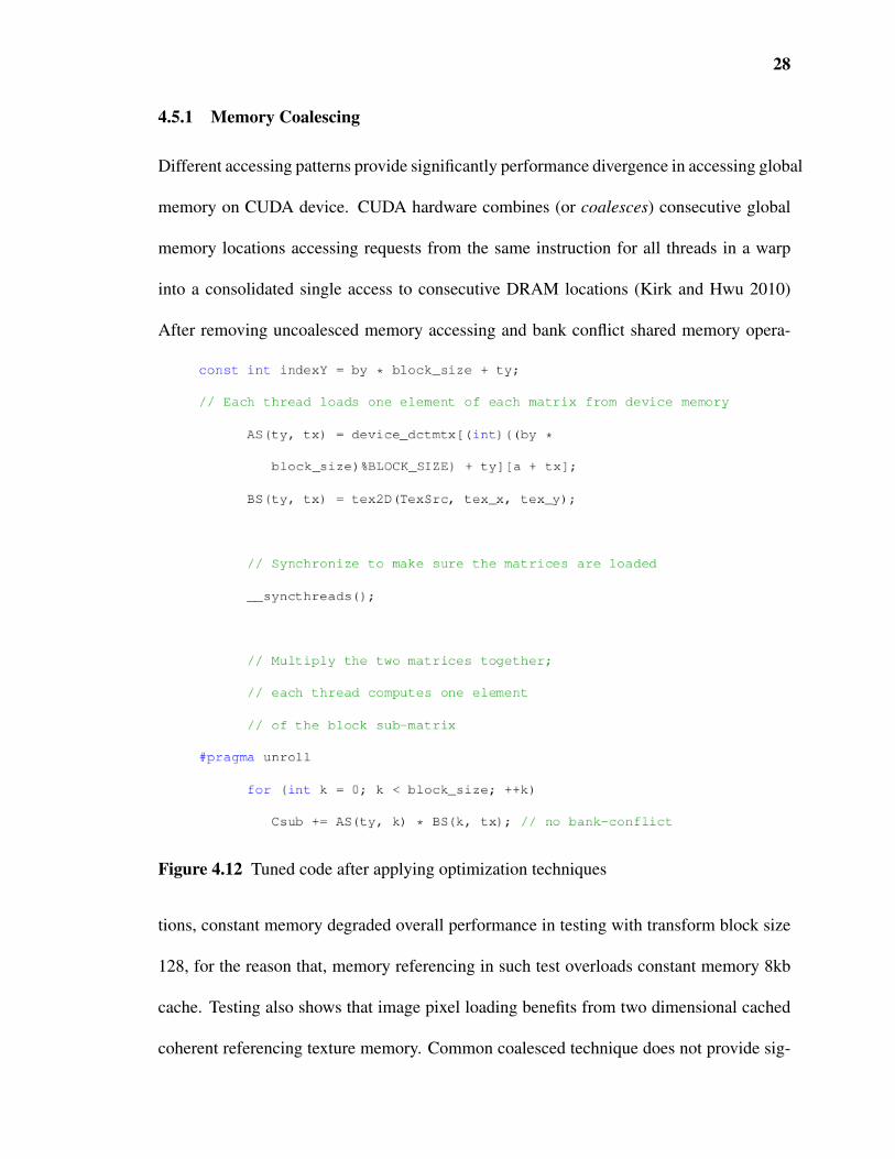
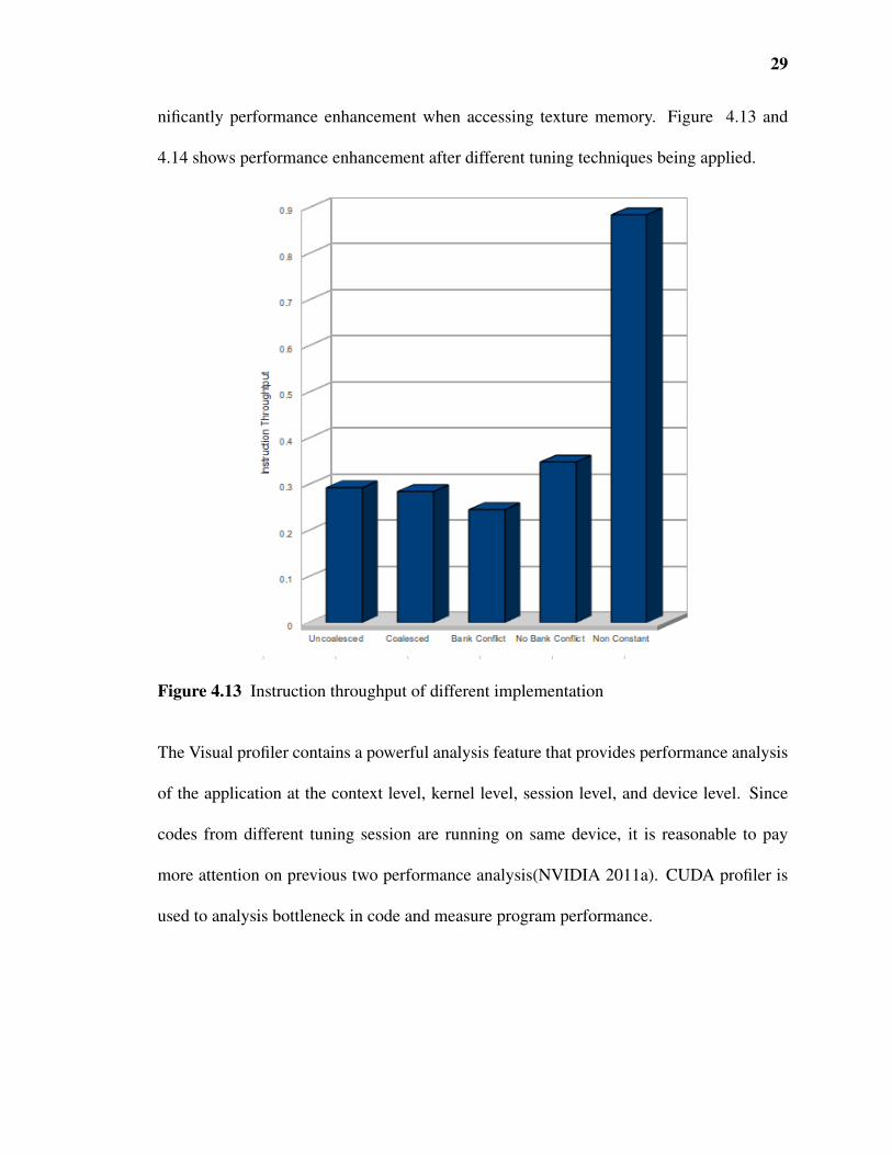
4.5.1 Memory Coalescing
Different accessing patterns provide significantly performance divergence in accessing global
memory on CUDA device. CUDA hardware combines (or coalesces) consecutive global
memory locations accessing requests from the same instruction for all threads in a warp
into a consolidated single access to consecutive DRAM locations (Kirk and Hwu 2010)
After removing uncoalesced memory accessing and bank conflict shared memory opera-
Figure 4.12 Tuned code after applying optimization techniques
tions, constant memory degraded overall performance in testing with transform block size
128, for the reason that, memory referencing in such test overloads constant memory 8kb
cache. Testing also shows that image pixel loading benefits from two dimensional cached
coherent referencing texture memory. Common coalesced technique does not provide sig-
29
nificantly performance enhancement when accessing texture memory. Figure 4.13 and
4.14 shows performance enhancement after different tuning techniques being applied.
Figure 4.13 Instruction throughput of different implementation
The Visual profiler contains a powerful analysis feature that provides performance analysis
of the application at the context level, kernel level, session level, and device level. Since
codes from different tuning session are running on same device, it is reasonable to pay
more attention on previous two performance analysis(NVIDIA 2011a). CUDA profiler is
used to analysis bottleneck in code and measure program performance.
30
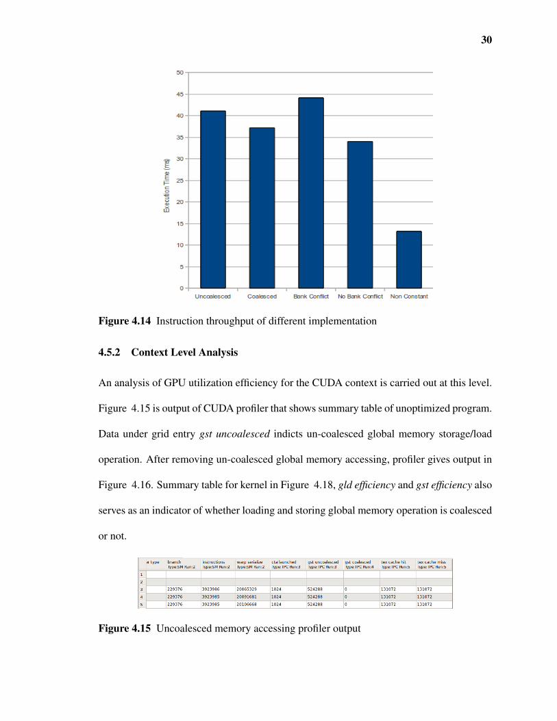
Figure 4.14 Instruction throughput of different implementation
4.5.2 Context Level Analysis
An analysis of GPU utilization efficiency for the CUDA context is carried out at this level.
Figure 4.15 is output of CUDA profiler that shows summary table of unoptimized program.
Data under grid entry gst uncoalesced indicts un-coalesced global memory storage/load
operation. After removing un-coalesced global memory accessing, profiler gives output in
Figure 4.16. Summary table for kernel in Figure 4.18, gld efficiency and gst efficiency also
serves as an indicator of whether loading and storing global memory operation is coalesced
or not.
Figure 4.15 Uncoalesced memory accessing profiler output

31
If two addresses of a memory request fall in the same memory bank, there is a bank
conflict and the access has to be serialized. The counter warp serialize gives the number of
thread warps that serialize on address conflicts to either shared or constant memory. In our
application, bank conflict brought by inappropriate shared memory accessing and constant
memory usage both contribute to warp serialize. Figure 4.17 gives result after recondition
shared memory accessing pattern and substituting constant memory usage to general global
memory usage.
4.5.3 Kernel Level Analysis
Greater detail regarding to particular kernel can be found below. For compute capability
below 2.0 Memory Throughput Analysis and Instruction Throughput Analysis are grayed
out. Only Occupancy Analysis is available.
Occupancy analysis gives theoretical kernel occupancy and identifies the limiting
factor for occupancy. It is calculated using the static parameters (multi-run) of the kernel
like launch configuration, shared memory, and register usage. By observing profiler occu-
pancy analysis output, it can be discovered that both un-coalesced memory accessing and
bank conflict can result in more local register usage. From previous discussion, It is advised
register usage per kernel should not exceed 10 per thread in case of local register usage be-
coming bottle neck. This also shows that indirect performance degradation of uncoalesed
Figure 4.16 Coalesced memory accessing profiler output

32
Figure 4.17 Profiler output after removing warp serialize
Figure 4.18 Summary table for kernel profiler output
Figure 4.19 Occupancy analysis for kernel with lower efficiency
Figure 4.20 Occupancy analysis for kernel with higher efficiency
33
global memory. Figure 4.20 is output of high occupancy achieved after tuning.
4.5.4 Testing Result Analysis
Testing is performed on NVIDIA early CUDA support GPU with compute capability 1.1
and only one multi-processor on device. In other words, testing device has only eight
parallel processing units–streaming processors or cores. Testing result shows potential to
achieve more speed enhancement by simply switching to higher compute capability or
devices with more cores. The high end Tesla accelerators have 30 multiprocessors, for a
total of 240 cores; a high end Fermi has 16 multiprocessors. for 512 cores. It is reasonable
to extrapolate performance enhancement to 100 times speed-up over current CPU version.
Quantization is not performed between forward and inverse transform. The pri-
mary source of error introduced is numerical error. For all integer type image data, all
floating point numerical errors are round-off or up after inverse transform. Consequently,
reconstructed image is identical to input image, mean square error measurement was not
performed.
4.6 Eigen Decomposition Implementation
In previous chapter, it has been shown that to completely decorrelate signal, in our ap-
plication for every N ×N real non-singular symmetric matrix, correlation matrix can be
rewritten in A = GDGT form. This hints transform matrix can be found through perform-
ing Singular Value Decompostion (SVD) which equals to eigen decomposition when apply
to signal covariance matrix. So the problem tranforms to how to obtain eigenvalues and
eigenvectors of covariance matrix. Jacobi-type algorithms are often considered too slow

34
for practical usage. However, due to their accuracy properties and inherent amenability for
parallelisation, it becomes a potential candidate of parallel algorithm.
4.6.1 Jacobi
Given a symmetric matrix G = G0, Jacobi’s method produces a sequence of orthogonally
similar matrices, which eventually converge to a diagonal matrix with the eigenvalues on
the diagonal. Gi denotes orthogonally similar matrix of original matrix after i-th iteration.
Gi+1 is obtained from Gi through plane rotation Gi+1 =V Ti AiVi, where Vi is an orthogonal
matrix called Jacobi rotation (Demmel 1997).
G(k) = G(k−1)V Tk , [V T ](k) = [V T ]k = [V T ]k−1V T
k ,k = 1,2, . . . ,s. (4.2)
where k denotes iteration steps. If G(s) has sufficiently orthogonal columns, [V T ]s serves
as a quite good approximation of V T . Now, the matrix V of right singular vectors is easily
obtainable from V T . The J-orthogonal matrices V Tk in equation above become simply as
plane rotations (trigonometric). Such a rotation orthogonalizes a pair of columns of G. The
rotators can be represented as
V T =
cosφ sinφ
−sinφ cosφ
=
1 tanφ
tanφ 1
cosφ 0
0 cosφ
(4.3)
If two columns within one pair are relatively orthogonal (up to the machine epsilon),
|ai j|< ε√
aiia j j (4.4)

35
According to form above, apply equation on the right hand side of G. Updated ith and jth
column of G,
gki = (gk−1
i − tanφgk−1j )cosφ (4.5)
gkj = (gk−1
j + tanφgk−1i )cosφ (4.6)
The columns of V T can be updated in the same fashion. For N by N square symmetrical
real matrix:
Rx =
a11 . . . a1N
... ai j...
aN1 . . . aNN
(4.7)
For each index pairs (i, j)(i < j), after applying certain algorithm to block
aii ai j
ai j a j j
(4.8)
Block above can be decomposed in such form:
aii ai j
ai j a j j
=V (i, j)
σi 0
0 σ j
V T (i, j) (4.9)
When plane rotation operates on both sides of orthogonal similar matrix sequence, the
algorithm is also named as two-sided Jacobi Algorithm. To update the ith and jth rows of
36
Rx, apply orthogonal transform V (i, j)
V T (i, j)
ai,1:n
a j,1:n
(4.10)
Then update the ith and jth columns
[a1:n,i a1:n, j
]V (i, j) (4.11)
To N by N matrix, up to N/2 pairs of rows/columns updating share no common indices can
be performed in parallel. After sweeping over all possible non-contradiction row/column
pairs, when convergence condition meets, decomposition finishes. Eigenvectors can be
found through accumulating all orthogonal matrices V (i, j) or V ( j, i) in an identity matrix.
4.6.2 Results and Further Discussion
Basically, CUDA implementation follows procedures introduced above. Row/Col update
scheme: Load ith and jth row/col pair from global(DRAM) to each block shared memory.
Then perform arithmetic operation to update row pairs and column pairs of input matrix.
Input matrix are symmetric whose elements are integer storing in float point type
integer ranging from 0 to 255. If we define looping over all non-overlap pairs one sweep
(n−1 row/column updating iteration, where denotes input matrix size), n/2+1 sweeps are
used to evaluate running time. Measurement takes time consumed by memory allocation/-
copy, communication between host(CPU) and device(GPU), data generation/deletion into
account.

37
Table 4.1: Execution time for cyclic and naive parallel implementationMatrixSize Cyclic(s) Parallel(s)
2048 test 1 2291.293 48.637test 2 2215.404 51.245test 3 2237.124 49.387
1024 test 1 160.293 12.165test 2 163.651 12.135test 3 161.329 12.105
512 test 1 10.651 3.133test 2 10.679 3.125test 3 10.793 3.128
Cyclic Jacobi
Cyclic Jacobi algorithm or generalized Jacobi algorithm is favourable implemen-
tation scheme on traditional CPU architecture for taking advantage of appropriately using
CPU cache line.
Parallel Jacobi
4.6.3 Divide and Conquer
diagonalization and triangularization are the two different strategies behind prac-
tically all modern eigen-routines. Jacobi iteration method can be taken as an example of
diagonalization method. In this section, divide and conquer is introduced as the example of
implementation of triangularization. It is reported that this method is reported as the fastest
now available for obtaining all eigenvalues and eigenvectors of a tridiagonal matrix whose
dimension is "larger" (Demmel 1997).

38
Table 4.2: Execution time for LAPACK (CPU) and MAGMA (GPU)MatrixSize CPUTime(s) GPUTime(s)
1024 3.11 1.972048 21.46 5.743072 73.20 16.974032 154.47 32.195184 330.11 70.276016 501.16 105.67
4.6.4 MAGMA Testing Result
MAGMA is an open source, high performance heterogeneous platform linear alge-
bra operation library. Combining widely used standard linear algebra library LAPACK on
CPU and wrappred CUBLAS function on CUDA GPU. This routine is available as both in
LAPACK and MAMGA eigen solvers. Table 4.2 gives performance comparison on Fermi
platform with compute capability 2.0.

CHAPTER 5
REAL TIME DISPLAY APPLICATION FRAME
5.1 Program Flow
Graphics interoperability of CUDA architecture allows using GPU for both rendering and
general purpose computation in the same application even when the images we want to ren-
der rely on the results of kernel computation. NVIDIA SDK sample is used as framework
and adapted for our application. As a window system independent OpenGL Toolkit, GLUT
is utilized for Linux compatibility. On screen image display is created through Pixel Buffer
Object (PBO) on a pixel-by-pixel basis. The schematic summarizes how OpenGL GLUT
system interacts with PBO (Farber 2010). The routine display() calls the The CUDA C ker-
nel that generates or modifies data in the OpenGL buffer, then data is passed to the OpenGL
driver to render new image to the screen as in Figure. Live video is imported from webcam
via TCP connection.
5.2 FFmpeg
FFmpeg is a complete, cross-platform open source project that produces both libraries and
programs which can record, convert and stream various format digital audio and video
(FFm 2010). In our application, FFmpeg retrieves output captured by web camera with
ability to output uncompressed raw video or other video device and file then convert it to
24 bit RGB format. After conversion, it feeds/supplys TCP socket with streaming data, as
illustrated in Figure. No actual TCP device is involved for transmitting data between appli-
cations (FFmpeg and application). A loop back network is set-up on localhost (Localhost is
39

40
Figure 5.1 OpenGL Display Flow
the name of the loop back device used by application that need to communicate with each
other one the same computer) and acts as an Ethernet interface. Using FFmpeg and TCP
connection is a succinct solution to handle video input with less programming involved.
TCP server in application is listening specified port and accepts connection attempts
from client. After connection established, it reads streaming data from TCP socket into
CPU managed data array when client sends data and writes it to buffer on the GPU for
kernel utilization. CUDA kernel discussed in previous chapter is fit into the framework.
41
Figure 5.2 Display Routine Flow
5.3 Test Result
Figure 5.4 and 5.5 shows test result of application running with viewport size 640 by 480
and transform block size 256. Although current application runs at high compute complex-
ity with great performance, an possible alternative solution to enhance performance further
could be using FFmpeg libraries within application directly to get raw input video from
camera input or get around TCP connection on localhost.
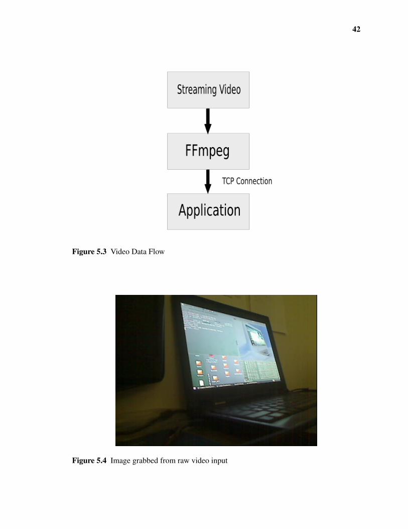
42
Figure 5.3 Video Data Flow
Figure 5.4 Image grabbed from raw video input

43
Figure 5.5 Image grabbed from video after one dimensional DCT transform
CHAPTER 6
CONCLUSION AND FUTURE WORK
6.1 Conclusion
In this thesis, GPU-based DCT and KLT implementation has been presented. The workflow
of developing program on GPU and using profiling tool to tune and measure performance
is showed. A real time video input, processing and display flow application frame is also
developed. Multiple purpose computational kernel could be fit into the frame for potential
GPU application. The practising shows fixed transform on image signal greatly benefits
from CUDA-specific features. Moreover, proper implementation can also lead to signif-
icantly performance improvement on serialized iterative algorithms over same algorithm
implementation on Central Processing Unit.
6.2 Future Work
To better excavate computational power of GPU, it is necessary to understand GPU ar-
chitecture, tool-chain, and general concept of parallel computing. Capability of CUDA
enable device may from product to product. Although CUDA architecture can be trans-
parent through different generation products, to maximize performance, applying different
configuration parameter to different CUDA product may be a reasonable option subject to
scrutinize. Right now, most developers resort to a "trial and error" approach of tuning code
to achieve better performance. CUDA API can be used to retrieve device information which
provide possibility to auto-tune performance according to different device and device con-
tent. Automatic performance tuning has been used for years to optimize CPU code. Test
44

45
platform used in thesis is low end early version of CUDA capable GPU. Such serial of prod-
uct suffers from weakness on structure lacking of global memory cache, which could lead
relatively high latency penalty for accessing global memory. The current architecture and
compiler design also do not allow combing usage of register and shared memory. From
the previous chapters, it is common to see limit number of registers often contributes to
hindering higher capacity being achieved. But the trend can be seen that, in Fermi architec-
ture, global L1 cache has already been added to enhance DRAM accessing performance. In
other word, techniques like memory coalescing or not may not affect general performance
significantly. Compiler also plays a major role in program optimizing. After analysing
PTX code, that instruction mix and register level code optimization technique can be used
to enhance performance furthermore (which will be added later).
Finally, "Butterfly" like or other fast algorithm actually used in real world can be
evaluated for enhancing performance to the next level.
APPENDIX A
TESTING RESULT FOR IMPLEMENTATION SCHEME 3
Figure A.1 Execution Time Comparison with picture size 512 x 512
46
47
Figure A.2 GPU vs CPU speed up with picture size 512 x 512
Figure A.3 Execution Time Comparison with picture size 2048 x 2048
48
Figure A.4 GPU vs CPU speed up with picture size 2048 x 2048

APPENDIX B
GPU AND CPU SPECIFICATION
GPU Specification
Model Name: GeForce 9300GS
Frequency: 1450.0MHz
Memory: 127.3 MB
Compute Capability: 1.1
Machine Specification:
Processor: 0
Model Name: Intel(R) Core(TM)2 Duo T5670
Frequency: 1800.000MHz
cache size: 2048 KB
Processor: 1
Model Name: Intel(R) Core(TM)2 Duo T5670
Frequency: 800.000MHz
cache size : 2048 KB
49

REFERENCES
(2010). Compute unified device architecture (cuda).
(2010). Ffmpeg project description.
Akansu, A. (2000). Multiresolution Signal Decomposition. Academic Press, second editionedition.
Axler, S. (1997). Linear Algebra Done Right. Springer, second edition edition.
Demmel, J. (1997). Applied Numerical Linear Algebra. SIAM, first edition edition.
Dongarra, J. (1997). Block algorithms: Matrix multiplication as an example.
Farber, R. (2010). Cuda supercomputing for the masses part15.
Fisher, Y. (1995). Fractal Image Compression. Springer.
Kirk, D. B. and Hwu, W. (2010). Programming Massive Parallel Processor. MorganKaufmann.
NVIDIA (2010). Nvidia cuda programming guide version 4.0.
NVIDIA (2011a). Compute visual profiler user guide.
NVIDIA (2011b). Next generation cuda compute architecture.
Rao, K. (2000). The Transform and Data Compression Handbook.
Rao, K. (2011). Optimal Decorrelation and The KLT.
Sanders, J. and Kandrot, E. (2010). CUDA by example. Addison-Wesley Professional.
Stein, M. (2010). Cuda basics. Technical report, New York University.
Tee, W. (2011). Finite-difference time-domain method implemented on the cuda architec-ture. Master’s thesis.
Wolfe, M. (2010). Understanding the cuda data parallel threading model a primer.
50