copyright by urmimala roy 2015
TRANSCRIPT

Copyright
by
Urmimala Roy
2015

The Dissertation Committee for Urmimala Roycerties that this is the approved version of the following dissertation:
Towards high-density low-power spin-transfer-torque
random access memory
Committee:
Sanjay K. Banerjee, Supervisor
Leonard F. Register, Co-Supervisor
Emanuel Tutuc
S. V. Sreenivasan
Maxim Tsoi

Towards high-density low-power spin-transfer-torque
random access memory
by
Urmimala Roy, B.E.; M.Tech.
DISSERTATION
Presented to the Faculty of the Graduate School of
The University of Texas at Austin
in Partial Fulllment
of the Requirements
for the Degree of
DOCTOR OF PHILOSOPHY
THE UNIVERSITY OF TEXAS AT AUSTIN
August 2015

To my family

Acknowledgments
I would like to thank my academic advisor Prof. Sanjay K. Banerjee for
his guidance and support. It has been an exceptional opportunity to be able
to work under his supervision for the last ve years. I sincerely thank him for
accepting me in his group. He has always given me complete freedom to choose
my research directions, shaping my identity as an independent researcher. I
take this opportunity to thank my co-supervisor Prof. Leonard F. Register for
his insightful advice every time I stumbled upon a problem. Not only did I
learn from his enormous knowledge of semiconductor physics, discussions with
him helped me learn how a research problem should be handled. It has been a
privilege to work with Prof. Register. I will remain indebted to Prof. Banerjee
and Prof. Register for their endless help and support.
I thank Prof. Maxim Tsoi for his guidance in the spin-transfer-torque
experiments, and my dissertation research in general. I also thank Prof. Tsoi
for serving on my PhD committee and his valuable suggestions on this disser-
tation. I thank Prof. Emanuel Tutuc and Prof. S. V. Sreenivasan for being in
my PhD commitee and for their valuable advice.
During my ve years at UT Austin I have had the privilege of working
with a number of extremely talented students. I take this opportunity to thank
Fahmida Ferdousi and Heidi Seinige for the excellent collaboration in my rst
v

year at UT. Fahmida introduced me to most of the tools I have learned to use in
the clean room. In the second half of my PhD, when I started working more on
the modeling and simulation, I have been fortunate to collaborate with Tanmoy
Pramanik and Rik Dey, on the multi-bit spin-transfer-torque random access
memory (STTRAM) and the topological insulator based STTRAM projects.
Working with Tanmoy and Rik has been a wonderful experience to say the
least. Thanks to them for being so patient with me, when I would stop by one
of their desks to talk about a long calculation I was in the middle of, and they
would help me as much as they could. I can not probably thank Tanmoy and
Rik enough.
I thank other past and present graduate students and post-docs at
the Microelectronics Research Center, Nima Asoudegi, Dax Crum, William
Hsu, Mustafa Jamil, Seyoung Kim, Emmanuel Onyegam, Yujia Zhai, Dhar-
mendar Reddy, Michael Ramon, Jason Mantey, Chris Corbet, Xuehao Mou,
Jiwon Chang, Hema Chandra Prakash Movva, Tanuj Trivedi, Amritesh Rai,
Amithraj Valsaraj, Sayan Saha, Donghyi Koh, Sk. Fahad Chowdhury, Ky-
ounghwan Kim, Milo Holt, Maruthi Yogesh, Atresh Sanne, Sushant Sonde,
Domingo Ferrer, Samaresh Guchhait, Bahniman Ghosh, Sarmita Majumdar,
Priyamvada Jadaun and Nitin Prasad, for their warm friendship and incred-
ible help. Special thanks to Anupam Roy for advice on this dissertation and
the discussions on Bengali literature and Indian politics on our way back from
PRC.
I express my sincere gratitude to Jean Toll, Christine Wood and Melanie
vi

Gullick for helping so much in every possible way. I thank Ricardo Garcia and
Johny Johnson for all their help during my brief stint in the clean room.
I had the opportunity to work as an intern in the Process Modeling and
Applications Group at Intel Corp. during the summer of 2014. I would like to
thank David L. Kencke for his guidance and mentoring. I would also like to
thank Cory E. Weber, Charles Kuo and Angik Sarkar, for their help making
my Intel experience such a wonderful one.
I would like to thank my friends at Austin, Arindam Sanyal, Avik
Ray, Somsubhra Barik, Ayan Acharya, Debarati Kundu, Abhik Ranjan Bhat-
tacharya and Rudra Narayan Chatterjee, Proma Bhattacharya and those out-
side Austin, Srimoyee Sen and Ankur Guha Roy for their company. Last ve
years would not be such a nice experience if they were not here. I take this
opportunity to thank Avhishek Chatterjee for being extremely patient and
considerate and an amazing friend. It has been a pleasure to know him. For
the last one and half years, I have been blessed with another family, besides
my own. I thank my parents-in-law, my sister-in-law Sudipa, her husband
Dimitri and my little niece Tinni for being in my life.
My heartfelt thanks to my sisterDidibhai and her husbandDebmalya da
for their love, tireless support and encouragement. They both being successful
researchers, their experience and advice helped me take decisions at every step
of my academic career so far. My husband Subhendu, who has been a friend
and a classmate ever since I joined IIT Bombay and a fellow PhD student at
UT Austin for the last four years, has always been a pillar of support. I thank
vii

him for being there for me always.
Lastly, I thank my parents Maa and Bapi for having nurtured in me a
deep sense of the value of education and for their love and trust.
viii

Towards high-density low-power spin-transfer-torque
random access memory
Publication No.
Urmimala Roy, Ph.D.
The University of Texas at Austin, 2015
Supervisors: Sanjay K. Banerjee and Leonard F. Register
In this work, we investigate the prospects for spin-transfer-torque ran-
dom access memory (STTRAM) as the new generation low-power high-density
non-volatile memory. Possible means to lower the switching current and in-
crease the packing density of STTRAM are proposed. In an STTRAM cell, the
logical value of the memory bit is stored as orientation of magnetic moment
in its ferromagnetic free layer. The bit typically consists of two thin lm
ferromagnets (FM) separated by an insulating tunnel barrier as in a magnetic
tunnel junction (MTJ) structure. One of the two FM layers has xed magne-
tization direction, while the other layer is free to be switched. We rst study
STT-assisted switching in spin valve structures with in-plane, perpendicular,
and canted magnetizations in free and (or) reference layers using point con-
tact measurements to explore the use of non-collinear magnetizations in free
and xed FM to reduce both switching current and time. Next, we consider
ix
the possibility of storing two memory bits within a single MTJ with a cross-
shaped free layer that could still be addressed by one selection transistor. We
provide a detailed discussion of the switching dynamics and associated regions
of reliable switching currents, in addition to illustrating the eects of varying
device geometry on the latter. Moving on from the standard MTJ structure,
we then consider the possible use of topological insulators, as opposed to the
xed FM, as the spin-polarizer layer. It has been established that spin and
momentum are locked helically in the surface states of a three-dimensional
topological insulator (TI). Suggestions of possible use of the TI spin-polarized
surface states in spintronic devices to induce reversal of a magnet have been
made using theoretical and experimental studies. Here, we simulate mag-
netization reversal of a metallic nanomagnet by an underlying TI. The TI,
thanks to the spin-momentum helical locking of the surface states, causes a
spin-polarized current injection to the FM above it. We study the eciency
of the spin injection as a function of varying transparency of the TI-FM inter-
face. The transport in the TI and the FM is assumed to be diusive at room
temperature for the assumed resistance values. Finally, we take into account
random thermal uctuations leading to write error rate (WER) in STTRAM
write operation and use Fokker-Planck method and stochastic Landau-Lifshitz-
Gilbert-Slonczewski equation to model WER in STTRAM. We conclude with
possible future research directions.
x

Table of Contents
Acknowledgments v
Abstract ix
List of Tables xiv
List of Figures xv
Chapter 1. Introduction 1
1.1 The memory hierarchy . . . . . . . . . . . . . . . . . . . . . . 21.2 STTRAM as the potential universal memory . . . . . . . . . . 51.3 Basic principles of STTRAM operation . . . . . . . . . . . . . 8
1.3.1 Write mechanism: Spin-transfer-torque . . . . . . . . . . 81.3.2 Read mechanism: Tunnel magnetoresistance . . . . . . . 91.3.3 Current driven switching modes . . . . . . . . . . . . . 11
1.3.3.1 Thermal regime . . . . . . . . . . . . . . . . . . 111.3.3.2 Precessional regime . . . . . . . . . . . . . . . . 111.3.3.3 Dynamic regime . . . . . . . . . . . . . . . . . . 11
1.4 Recent progress in STTRAM . . . . . . . . . . . . . . . . . . . 121.5 Current challenges for STTRAM . . . . . . . . . . . . . . . . . 131.6 Overview of this dissertation . . . . . . . . . . . . . . . . . . . 17
Chapter 2. Perpendicular and canted magnetic anisotropy forSTTRAM 19
2.1 Motivation . . . . . . . . . . . . . . . . . . . . . . . . . . . . . 192.2 Fabrication and characterization of in-plane, canted, and PMA
spin valves . . . . . . . . . . . . . . . . . . . . . . . . . . . . . 222.2.1 Spin valve fabrication . . . . . . . . . . . . . . . . . . . 222.2.2 Characterization by point-contact measurements . . . . 23
2.3 Conclusions . . . . . . . . . . . . . . . . . . . . . . . . . . . . 25
xi

Chapter 3. Spin-transfer-torque switching of a ferromagneticcross towards multi-bit STTRAM 27
3.1 Motivation . . . . . . . . . . . . . . . . . . . . . . . . . . . . . 273.2 Results . . . . . . . . . . . . . . . . . . . . . . . . . . . . . . . 29
3.2.1 Equilibrium magnetizations of the cross . . . . . . . . . 293.2.2 Magnetization dynamics under STT . . . . . . . . . . . 32
3.2.2.1 State 1 to State 2 switching . . . . . . . . . 353.2.2.2 State 1 to State 3 switching . . . . . . . . . 353.2.2.3 State 1 to State 4 switching . . . . . . . . . 37
3.2.3 Thermal stability . . . . . . . . . . . . . . . . . . . . . . 403.3 Packing density considerations . . . . . . . . . . . . . . . . . . 423.4 Conclusion . . . . . . . . . . . . . . . . . . . . . . . . . . . . . 43
Chapter 4. Spin-transfer-torque switching of a metallic nano-magnet due to an underlying topological insulator 45
4.1 Motivation . . . . . . . . . . . . . . . . . . . . . . . . . . . . . 464.2 Results . . . . . . . . . . . . . . . . . . . . . . . . . . . . . . . 48
4.2.1 Transport model . . . . . . . . . . . . . . . . . . . . . . 484.2.2 Self-consistent transport and magnetization dynamics cal-
culation . . . . . . . . . . . . . . . . . . . . . . . . . . . 624.3 Conclusion . . . . . . . . . . . . . . . . . . . . . . . . . . . . . 67
Chapter 5. Write error rate in STTRAM 72
5.1 Motivation . . . . . . . . . . . . . . . . . . . . . . . . . . . . . 745.1.1 Challenges for WER simulation using micromagnetic eects 74
5.2 Results . . . . . . . . . . . . . . . . . . . . . . . . . . . . . . . 755.2.1 Fokker-Planck calculation of WER within the macrospin
approximation . . . . . . . . . . . . . . . . . . . . . . . 755.2.2 WER simulation including micromagnetic eects . . . . 76
5.2.2.1 Method . . . . . . . . . . . . . . . . . . . . . . 765.2.2.2 Results . . . . . . . . . . . . . . . . . . . . . . . 78
5.3 Conclusion . . . . . . . . . . . . . . . . . . . . . . . . . . . . . 79
xii

Chapter 6. Conclusion 83
6.1 Summary . . . . . . . . . . . . . . . . . . . . . . . . . . . . . . 836.2 Future directions . . . . . . . . . . . . . . . . . . . . . . . . . 86
Bibliography 88
Vita 101
xiii

List of Tables
2.1 Slope of STT for samples I-III. . . . . . . . . . . . . . . . . . . 25
4.1 Parameters assumed for transport in the TI-FM bilayer . . . . 64
xiv
List of Figures
1.1 Memory hierarchy . . . . . . . . . . . . . . . . . . . . . . . . . 31.2 Comparison of STTRAMwith other existing and emerging mem-
ory technologies, created following Ref. [1]. . . . . . . . . . . . 61.3 STTRAM cell with 1 MTJ and 1 selection transistor. . . . . . 71.4 STT in a FM-nonmagnet-FM trilayer stack . . . . . . . . . . . 81.5 Magnetoresistance (MR) in a FM-NM-FM stack. . . . . . . . 10
2.1 (a) is a typical magnetoresistance plot of sample II with a mag-netic eld applied perpendicular to the sample plane and a dcbias current of -1.3 mA. (b-d) are STT slope from point contactmeasurements for sample I-III respectively, with open symbolsfor up-sweep and closed symbols for down-sweep. This gurehas been reproduced from Ref. [2] with permissions. . . . . . . 23
3.1 Cross-shaped MTJ stack . . . . . . . . . . . . . . . . . . . . . 283.2 Equilibrium magnetizations; (a) State 1; (b) State 2; (c)
State 3; (d) State 4; l1/w is referred to as AR of short arm,l2/w is referred to as AR of long arm. This gure has beenreproduced from Ref. [3] with permissions. . . . . . . . . . . . 31
3.3 (a) 1 → 2 switching with J = 5 × 10⁷A/cm2 (b) Pre-switchingoscillations with dierent J values; inset: linear t of 0 crossingtime for dierent values of short branch AR (l1/w) and longbranch AR (l2/w). l1, l2 and w are dened in Figure 3.2. Thisgure has been reproduced from Ref. [3] with permissions. . . 36
3.4 1 → 3 switching with J = 3.8×10⁸A/cm2. This gure has beenreproduced from Ref. [3] with permissions. . . . . . . . . . . . 38
3.5 1 → 4 switching with two current pulses of opposite polaritiesand dierent magnitudes. This gure has been reproduced fromRef. [3] with permissions. . . . . . . . . . . . . . . . . . . . . . 39
3.6 Switching regions to State 2 and State 3 starting from State1 with increasing amplitude of current pulse in steps of J =5 × 10⁶ A/cm2 for dierent designs of cross. This gure hasbeen reproduced from Ref. [3] with permissions. . . . . . . . 40
xv

4.1 (a) Schematic of the TI-FM bilayer, x is the transport, z is theout-of-plane direction. (b) The lled circle denotes the shiftedFermi circle in presence of a current supported by the surfacestates. The arrows denote the spin vectors of the surface statesbecause of spin-momentum helical locking. This gure has beenreproduced from Ref. [4] with permissions. . . . . . . . . . . . 54
4.2 Transport in the bilayer for xed FM magnetization along +xand an applied voltage of 0.2 V for (a) small coupling (normal-ized interlayer conductivity = 1/100), (b) moderate coupling(normalized interlayer conductivity = 1/9), and (c) Large cou-pling (normalized interlayer conductivity = 1). (d) Resistanceof the bilayer vs. interlayer conductance. Inset in (d): TI re-sistivity as a function of the normalized interlayer conductance.This gure has been reproduced from Ref. [4] with permissions. 61
4.3 Variation in device metrics with varying interlayer coupling,with the FM magnetized along the +x-direction and an appliedvoltage of 0.2 V. (a) spin torque ratio (spin Hall angle) obtainedwith respect to nominal TI conductivity. (b) spin torque ratiowith respect to TI conductivity self-consistently decreased bythe process of exerting STT. (c) Spin injection eciency, (d)Spin-transfer-torque (STT) via injection across the interface,and eld-like torque (FLT) via exchange coupling between thespin-polarized electrons in the TI and the nanomagnet. Thisgure has been reproduced from Ref. [4] with permissions. . . 69
4.4 (a) Switching of the FM from +y to -y for an applied voltageof -0.2 V, so that current is in -x-direction. (b) Switching ofthe FM from -y to +y for an applied voltage of 0.2 V, so thatcurrent is in +x-direction. (c) Switching time ts (dened in thetext) and write energy per write operation vs. applied voltageacross the bilayer, for the normalized interlayer conductivity of1. The TI fails to switch the FM below a critical voltage as canbe seen from the plot of inverse of switching time with voltagein the inset of (c). (d) Switching time ts (dened in the text)and write energy per write operation vs. normalized interlayerconductivity, for an applied voltage of 0.2 V. Similarly, the TIfails to switch the FM below a critical interlayer conductivity,as can be seen from the plot of inverse of switching time withcoupling in the inset of (d). This gure has been reproducedfrom Ref. [4] with permissions. . . . . . . . . . . . . . . . . . . 70
4.5 a) bilayer resistance, b) Spin injection eciency and c) Switch-ing time and write energy per write operation for articially in-creased FM in-plane resistivity and varying interlayer couplingd) Write energy as a function of the FM resistivity divided bythe FM thickness. This gure has been reproduced from Ref. [4]with permissions. . . . . . . . . . . . . . . . . . . . . . . . . . 71
xvi

5.1 Write error from micromagnetic simulations. 20 trials are shown,each simulated with a random thermal seed for the random ther-mal magnetic eld. A current pulse is applied at 5 ns, startingfrom uniform magnetization in +z at 0 ns. The current pulse isturned of at 11 ns, the trials which are above mz=0 at the timethe current pulse is turned o, go back to the initial magneti-zation of mz=1 and cause an error. . . . . . . . . . . . . . . . 73
5.2 WER from Fokker-Planck method, for diameter D=40 nm andD=80 nm, for normalized current i = I/Ic0 of 2 and 6, as afunction of normalized time t/t0. This gure has been reusedfrom Ref. [5]. . . . . . . . . . . . . . . . . . . . . . . . . . . . 77
5.3 WER from Fokker-Planck method, for diameter D=40 nm andD=80 nm, for normalized current i = I/Ic0 of 2 and 6, as afunction of physical time. This gure has been reused fromRef. [5]. . . . . . . . . . . . . . . . . . . . . . . . . . . . . . . 78
5.4 WER from macrospin (Fokker-Planck) calculations comparedwith micromagnetic calculations for D=40 nm. This gure hasbeen reused from Ref. [5]. . . . . . . . . . . . . . . . . . . . . 80
5.5 WER from macrospin (Fokker-Planck) calculations comparedwith micromagnetic calculations for D=80 nm. This gure hasbeen reused from Ref. [5]. . . . . . . . . . . . . . . . . . . . . 81
5.6 Scaling of WER from micromagnetic simulations for D=20 nmto 80 nm as a function of normalized time t/t0 for normalizedcurrents i=2 and i=6. This gure has been reused from Ref. [5]. 82
xvii

Chapter 1
Introduction
Spintronics, the commonly used name for spin-transport-electronics,
employs electron spin in solid state devices and has been an area of great
fundamental and practical interest, owing to exciting physics and the promise
of applications in technology. Each electron carries a unit of charge (-e) as
well as a unit of spin angular momentum h2, or equivalently, a xed magnetic
moment. The spin angular momentum can only have two values along any
direction, ± h2, and is normally labeled as up or down spin. In normal
metals, e.g. Cu, electrons of both the spins are randomly oriented and the
density of states of the two spins are the same at the Fermi level. In certain
metals such as Fe, Co or Ni, and many other alloys of these, due to huge
internal exchange interactions, the atomic magnetic moments align parallel to
each other. The densities of states for up and down spin electrons at the Fermi
level are dierent and the two spin bands are shifted in energy. Fe, Co or Ni are
so-called ferromagnetic metals. Many properties in these materials, e.g. the
electrical conductivity, are thus spin-dependent as a result of the spin-splitting
in the energy bands.
Ferromagnetism in Fe, Co, Ni and their alloys has been known for a
1
long time. The recognition that the interaction of the electron spin angular
momentum with the solid can be manipulated for device applications, just
as well as that of its charge, only came recently. The discovery of the gi-
ant magnetoresistance by Albert Fert and Peter Grünberg [6, 7] (2007 Nobel
prize) marks an important milestone in the eld of spintronics and soon led
to several practical applications in magnetic data storage and read heads.
With advancements in nanoscale fabrication techniques the discovery of the
tunnel magnetoresistance (TMR) in a magnetic tunnel junction (MTJ) fol-
lowed [812] and found widespread applications in magnetic random access
memory (MRAM). Magnetization in the patterned ferromagnetic thin lms in
an MTJ traditionally has been controlled using magnetic elds. This disser-
tation is, however, focused on using a spin-polarized current in magnetization
switching for potential applications in random access memories.
1.1 The memory hierarchy
There are dierent levels of memory in a computer depending on the
proximity to the central processing unit (CPU). For example, CPU registers
store the data most frequently used by the CPU. The CPU registers can be
accessed very quickly (access time ∼ns). The cache memories, which also oer
fast access, are in the next level. Next, the main memory has larger size,
but typically would take longer to communicate with the CPU. The largest
information storage happens in a solid state drive (SSD) or in a hard disk drive
(HDD). The SSD (ash memory) oers faster access than the HDD. Access
2

CPU
Registers
Local secondary storage
(SSD, HDD)
Cache
(SRAM)
Sp
eed
an
d c
ost
Den
sity
Main memory
(DRAM)
Remote secondary storage
(tapes)
Figure 1.1: Memory hierarchy
time to HDDs are very large (∼ms). The division of memory usage according
to information storage density and speed of access from the CPU is referred
to as the memory hierarchy in computer architecture (shown schematically
in Figure 1.1).
Accordingly, dierent memory technologies are used in dierent levels
of the memory hierarchy depending on their access speeds and bit packing den-
sities. For example, the most commonly used memory technology for the cache
memory is static random access memory (SRAM), which is faster than the dy-
namic random access memory (DRAM) used in the main memory. However,
an SRAM cell occupies too large an area (∼100F2, where F is the minimum
3

feature size of the technology node). DRAM, on the other hand, occupies
smaller area per cell (∼6F2) and also oers fast access (access time ∼10-100
ns). With semiconductor technology approaching the so-called end of the
road-map it is getting harder to scale the commonly used semiconductor de-
vice based memories to smaller technology nodes. For example, increasing
leakage current of the SRAM cell has become a concern. For the DRAM
technology, as the cell is typically realized using a transistor and a capacitor,
realizing a certain capacitance in a certain maximum allowed footprint has
become challenging. It has been predicted that DRAM will be dicult to be
scaled further than the 20 nm node [13,14].
Moreover, the traditionally used magnetic-eld-assisted random access
memory (MRAM) is not scalable to smaller bits. In the traditional MRAM, a
smaller bit would require a larger magnetic eld for information to be recorded
in it, in turn requiring a larger write current [15]. This would increase the
power consumption by a large extent. Moreover, the commercially available
MRAM is slower than SRAM and less dense than DRAM [16].
In this scenario, the memory industry, therefore, is looking for alter-
natives, and preferably one that can be used in all the levels of the memory
hierarchy. With the theoretical predictions [17,18] and experimental observa-
tion [19] of the so-called spin-transfer-torque (STT), it was readily recognized
that using a spin-polarized current (SPC) to do the write operation instead of
a magnetic eld in a magnetic bit would greatly enhance the scalability of non-
volatile information storage. The counterpart of MRAM, in which the write
4

mechanism would be STT, is referred to as the spin-transfer-torque random
access memory (STTRAM).
1.2 STTRAM as the potential universal memory
In addition to the scalability, the access speed of STTRAM is expected
to be really high (access time ∼2-30 ns [13]), as has been demonstrated already.
Moreover, STTRAM promises a cell size of 6F2 or, possibly even smaller than
that [15]. With only few additional masks, STTRAM fabrication is compat-
ible with CMOS fabrication steps [20]. Hence, the widespread hope is that
STTRAM might be a candidate for the so-called universal memory, becom-
ing a potential replacement for memories in more than one of the levels in the
memory hierarchy, if not all of them [21].
A comparison of STTRAM with other emerging and existing mem-
ory technologies such as SRAM, DRAM, NAND and NOR ash, phase change
memory (PCM), magnetoelectric RAM (MeRAM) and ferroelectric RAM (FeRAM)
can be found in work by Yoda et al. [16] and has been shown schematically in
Figure 1.2, following previous work [1].
In a single STTRAM cell, a bit of information is stored as the mag-
netization direction of a patterned nanoscale thin lm ferromagnet (FM). In-
formation stored as the magnetization direction lends an inherent non-volatile
nature to this memory technology. Although information is stored as the
magnetization direction of a single FM known as the free FM, both read and
write mechanisms require a FM-nonmagnet-FM trilayer stack (schematically
5

1 ns 1 µs 1 ms
1 pJ
1 nJ
1 fJ
Write time
Wri
te e
ne
rgy
MeRAM
STTRAM
RRAM FeRAM
PCRAM
NOR NAND
Figure 1.2: Comparison of STTRAM with other existing and emerging mem-ory technologies, created following Ref. [1].
shown in Figure 1.3). The other FM in the trilayer stack is known as the
xed or the reference layer. The nonmagnetic layer is generally a tunnel
barrier, thus allowing reading of the bit using the TMR. The trilayer stack is
then called a magnetic tunnel junction (MTJ). Also, in an STTRAM cell, the
MTJ is accessed through a selection transistor.
There are two types of STTRAM bits currently being considered ac-
cording to the orientation of the free layer with respect to the plane of the
thin lm. If the easy axis is in the plane of the thin lm, the bit is referred
to as an `in-plane' bit. For an in-plane bit, the easy axis is engineered using
6

Bit Line
Source line
Word line
free layer
Tunnel barrier
fixed layer
(polarizer)
Figure 1.3: STTRAM cell with 1 MTJ and 1 selection transistor.
shape anisotropy of the magnet, so the free layer magnet is often a thin lm
ellipse. This way, the easy axis is along the longer of the two axes, i.e., the
major axis of the ellipse. The other type of MTJ is where the easy axis of
the free layer magnet is perpendicular to the plane of the thin lm. The easy
axis can be in a perpendicular direction owing to the so-called perpendicular
magnetic anisotropy (PMA) of the magnetic material. As will be discussed in
the subsequent sections in more detail, perpendicular STTRAM bits possess
7
inherently better performance compared to the in-plane bits owing to the dif-
ferent energy landscape. A comparative study using simulations can be found
in a previous study [22]. The international technology roadmap for semicon-
ductors (ITRS) predicts use of perpendicular materials for STTRAM from
the year 2017 and onwards [23]. In this chapter, rst the write mechanism of
STTRAM memory bit, which is the phenomenon of STT, will be described
along with the read mechanism of tunnel magnetoresistance (TMR). Then,
we briey discuss the recent experimental demonstrations of STTRAM. The
challenges for STTRAM to become a main stream memory technology will be
discussed along with some of the solutions currently being considered.
1.3 Basic principles of STTRAM operation
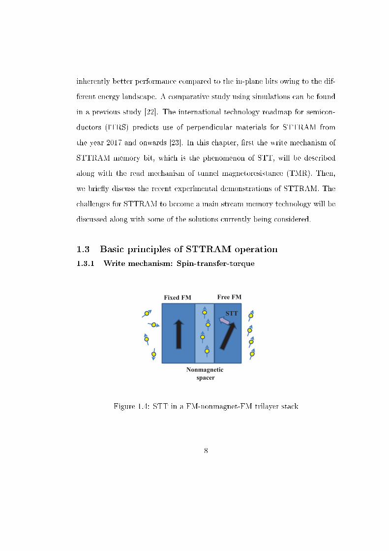
1.3.1 Write mechanism: Spin-transfer-torque
Fixed FM Free FM
Nonmagnetic
spacer
STT
Figure 1.4: STT in a FM-nonmagnet-FM trilayer stack
8

When a SPC traverses a ferromagnet (FM), the transverse component
of the spin angular momentum of the SPC is absorbed by the FM. STT arises
because of rapid dephasing, usually within a few atoms from the non-magnetic
layer into the FM, if the incident spin is not aligned with the magnetization
direction of the FM. As a result, the FM experiences a torque, which is known
as the spin-transfer-torque (STT). When the STT is large enough to overcome
the damping inherent in the FM, the STT might lead to magnetization reversal
of the FM [17, 18, 24]. The SPC is usually generated using spin-ltering by
another ferromagnet, the xed FM in the MTJ stack (shown schematically
in Figure 1.4).
1.3.2 Read mechanism: Tunnel magnetoresistance
Apart from the all electrical write mechanism, STTRAM takes advan-
tage of the MTJ stack for an electrical read out of the information written in
the free FM. The read-out is usually done by measuring the resistance of the
stack. The percentage change in resistance when the magnetizations in the
free and the xed FM are parallel (P) or antiparallel (AP) to each other is
referred to as magnetoresistance (MR) ratio (≡ (RAP − RP)/RP). With the
non-magnetic spacer (NM) between the two FM electrodes of the MTJ being
a thin dielectric tunnel barrier, the magnetoresistance arises because of spin-
dependent tunneling between the electrodes. The TMR eect was predicted
rst by Julliere [10] and experimentally observed independently by Moodera
et al. [9] and Miyazaki et al. [12]. In a ferromagnet, the density of states of
9

the two spin bands (up and down) are separated in energy. As a result, one
of the two spins can travel across the FM-NM-FM stack, only if the two FM
electrodes are parallely magnetized. On the other hand, if the the two FM
electrode magnetizations are antiparallel, neither of the two spins can make to
the other electrode from the NM. The simplest interpreation of phenomenon
of MR has been shown schematically in Figure 1.5. An MR ratio of more
than 100% has been predicted theoretically [25] and also has been experimen-
tally demonstrated [11] for single crystal Fe/MgO/Fe MTJs. The TMR of the
MTJ stack decides the read margin as well as the read speed of the STTRAM
bit [20].
NM FM FM
Parallel Antiparallel
FM FM NM
EF EF EF
N(E) N(E)
Figure 1.5: Magnetoresistance (MR) in a FM-NM-FM stack.
10

1.3.3 Current driven switching modes
Depending on the length of the write pulse there can be three distinct
modes of STTRAM switching [26]:
1.3.3.1 Thermal regime
If the current amplitude is small compared to the critical switching
current Ic0 and a long pulse is being used, the switching happens mainly by
thermal activation over the energy barrier. This regime is referred to as the
thermal regime. In the thermal regime, the initial (prior to the application
of the write pulse) probability distribution of the free layer magnetization is
irrelevant, whereas the temperature, and hence thermal uctuations during
the reversal is important [26].
1.3.3.2 Precessional regime
In the precessional regime, the pulse length is short and the pulse am-
plitude is several times higher than Ic0. In the precessional regime, the thermal
uctuation during the reversal does not aect the switching distribution, only
the initial thermal distribution of the magnetization is important [26].
1.3.3.3 Dynamic regime
The dynamic regime is the region in the pulse length-pulse amplitude
plane where neither of the above two cases are true and both initial thermal
distribution and the thermal uctuations during the reversal might play im-
11

portant role. The dynamic regime is important from practical point of view
since STTRAM is most likely to be operated in this regime for applications of
interest.
The stochastic nature of the switching will be discussed in more detail
in Chapter 5.
1.4 Recent progress in STTRAM
Considerable amount of eort has been put in the last decade to im-
prove the performance of STTRAM and meet the specications in the ITRS.
A comparison of performance achieved by dierent groups can be found in
the review by Yoda et al. [16]. Historically, the in-plane magnetized MTJs
matured technologically before the perpendicular MTJs. However the critical
switching current was as high as hundreds of micro-amperes, thereby ending
up requiring a very large selection transistor and reducing the packing den-
sity. A major advancement was made by Toshiba in proposing perpendicular
bits [27]. Even before the demonstration of STT switching in perpendicularly
magnetized MTJ by Toshiba [27], it was being noted by other groups that using
PMA, instead of shape anisotropy and in-plane magnetization in the free layer
might oer better switching current for the same anisotropy eld and studies
on spin-valves were carried out [28]. However, a spin-valve(with a metal as
the non-magnetic spacer instead of a dielectric tunnel barrier) suers from a
small magnetoresistance ratio(∼1%), which is small compared to the require-
ment of electrical read out. An ecient read-out needs TMR ∼150% [16, 23].
12

In [27], a buer layer of CoFeB was used to lessen mismatch between the MgO
tunnel barrier and the perpendicularly magnetized TbCoFe, though a TMR
ratio of only 15% was seen. Further improvements in the perpendicular MTJ
technology followed and led to a demonstration of as high as 200% TMR [29].
The other concerns towards making commercially viable STTRAM is
the write speed and the write energy, though both are related to the write
current. Writing by 1 ns long current pulse and write energy as small as 0.05
pJ/bit has been demonstrated by Toshiba [30]. Though perpendicular bits
are considered to be the solution for the problem of high switching current,
problems with materials with PMA include [31]:
• Crystal match with the MgO tunnel barrier for high spin injection e-
ciency and high TMR.
• The material has to have low enough damping constant(<0.01).
Apart from high TMR, small write current, write energy and write
time, a suciently high endurance of the cell has to be ensured. Endurance
of the bit refers to the maximum number of write cycles a cell can withstand
before suering from a damage [31].
1.5 Current challenges for STTRAM
Inspite of having a potential for scalability to smaller technology nodes
unlike its magnetic-eld-assisted counterpart, STTRAM faces a number of se-
rious challenges before it can be made commercially viable, as will be discussed
13

in more detail in the following paragraphs. The main obstacle is due to the high
write energy, stemming from the high write current density required for reli-
able switching of the bit [1,13]. Switching energy from recent demonstrations
are high, ∼100 fJ (Ref. [1] and references therein). The high switching energy
compared to the switching energy of a CMOS transistor switch might prohibit
the use of STTRAM in application that require frequent read and write oper-
ations [1]. The switching current density (Jc0) is the minimum charge current
density needed to be injected to the nanomagnet to overcome the damping
in the system. A model to calculate Jc0 was proposed by J. Sun [32]. The
model assumed a monodomain magnetic body subject to a magnetization dy-
namics given by Landau-Lifshitz-Gilbert-Slonczewski (LLGS) equation which
is driven out of equilibrium by a spin-polarized current injected perpendicular
to its plane. Using this model, switching current for monodomain in-plane
magnetized body can be written as [22,32]:
Jc0 =1
η
2eα
hMst(2πMs +HK) (1.1)
where, η is spin-transfer eciency, α is the damping factor,Ms is the saturation
magnetization characteristic of the material, HK is the anisotropy eld, t is
the thickness of the free layer. The energy barrier to be crossed while being
thermally switched, and hence the thermal stability factor (∆) of the bit is
eectively decided by the anisotropy eld HK. Hence, Eq. (1.1) essentially
dictates the Jc0-∆ trade-o [22]. A ∆ of ∼60 is required for ∼10 years of data
14
retention. The trade-o between switching current and thermal stability of a
bit is discussed in more detail while motivating Chapter 2.
In case of perpendicularly magnetized bit, due to absence of the 2πMs
term in Eq. (1.1), Jc0 is expected to be smaller for same HK and hence, same
thermal stability [22,28]. Work described in Chapter 2 is motivated by this.
Another problem introduced by the high values of Jc0 is the large area
of the selection transistors which will be required to drive the high current,
which in turn limits the maximum packing density achievable [1]. A possible
route to larger packing density can be the ability to address two bits stored in
a single nanomagnet, which is still addressed by a single selection transistor. A
multi-level cell might enable scaling down below the 6F2 cell area [20]. Work
described in Chapter 3 is motivated by search for a possible route towards
multi-bit STTRAM.
STTRAM is expected to possess innite endurance thanks to the fact
that there is no inherent wear-out mechanism involved with ipping the mag-
netization back and forth using STT. In contrast, competing emerging mem-
ory technologies such as the phase-change memory (PCM) and the resistive
random access memory (RRAM) suer from wear-out as the writing involves
physical displacement of the atoms [13]. However, wear-out in an STTRAM
does take place due to large write current crossing the tunnel barrier and di-
electric break down of the tunnel barrier after a certain number of operations
is a concern. A possible solution that has been proposed is to use a dierent
device geometry than the two terminal MTJ structure where the read and
15

write paths are the same. In the so-called spin Hall geometry, a heavy metal
such as Ta or Pt is used to inject spin to the free FM for the write opera-
tion [33,34]. In the spin Hall geometry the read and write paths are separate,
thereby saving the tunnel barrier in the MTJ read path from wear-out due
to large write current being sent through it. However, the three terminal ge-
ometry might require larger area per cell compared to the two terminal MTJ.
Also, a material with a high spin Hall angle is needed as the spin polarizer, so
that the write current density is small enough for practical applications. With
discovery of topological insulators (TI) with spin-momentum locked surface
states [35], a TI has become a promising candidate for the spin Hall mate-
rial. SPC injection to a FM using a TI has been reported experimentally [36]
and low-temperature magnetization switching has also been demonstrated [37].
Work described in Chapter 4 is motivated by eciency of STT switching of a
metallic nanomagnet(as opposed to an insulating one) by SPC injection by an
underlying TI.
The write time for an STTRAM bit for a given write pulse amplitude
is a stochastic quantity. Alternatively, the probability that a bit is written,
i.e., the magnetization of the free layer ips when a write pulse is applied for
a given duration can, in general, be less than 1. The fact that the switching
time is a random quantity, requires the circuit designers to have a write pulse
much longer than the average write time to ensure a certain safety margin.
The probability that a bit will not be written after a write pulse is applied is
referred to as the write error rate (WER). The WER should be below 10−9 if
16

there is an error correction code (ECC) and below 10−18 in absence of any ECC,
for correct operation as a working memory [31]. The necessity to understand
the reasons behind write error and improve WER motivates Chapter 5.
1.6 Overview of this dissertation
The goal of this dissertation is to investigate possible ways of decreasing
the switching current and increasing the packing density in STTRAM memory
[25].
• Chapter 2 focuses on use of perpendicular and canted magnetic anisotropies
for ecient STT switching in spin-valve structures [2].
• Chapter 3 focuses on micromagnetic simulations of STT switching of a
ferromagnetic cross [3]. We investigate possibility of using a ferromag-
netic cross for a multi-bit STTRAM.
• Chapter 4 describes modeling study of a STTRAM bit using a TI as the
spin polarizer layer in a spin Hall geometry [4].
• Chapter 5 briey describes the eects of including thermal uctuations
into STTRAM modeling. We describe our ongoing work on thermal
uctuation induced error in STTRAM write operation using Fokker-
Planck calculations and micromagnetic simulations including random
thermal magnetic eld.
17

• I will summarize and conclude this dissertation in Chapter 6 with a
discussion on possible future research directions.
18

Chapter 2
Perpendicular and canted magnetic anisotropy
for STTRAM
In this chapter we try to exploit magneto-crystalline anisotropy for
ecient STT switching using spin-valve experiments. The results have been
published in Ref. [2].1
2.1 Motivation
In a spin valve, anisotropy axes of the two ferromagnetic layers can be
in the plane of the sample, perpendicular to the plane or making an angle to
either. Materials with perpendicular magnetic anisotropy (PMA) are being
considered widely because of a promise of larger retention owing to higher
coercive eld and lower switching current due to lower damping constants [28].
Reduction in switching current with PMA materials have been reported [38
1The results in this chapter has been published in Ref. [2] (Journal of Applied Physics,vol. 111, no. 7, p. 07C913, 2012). The paper is titled Spin-transfer-torque switching inspin valve structures with perpendicular, canted, and in-plane magnetic anisotropies" by U.Roy, H. Seinige, F. Ferdousi, J. Mantey, M. Tsoi, and S. K. Banerjee. The contributions forthis paper is as follows. The spin valve samples were prepared by U. Roy and F. Ferdousiusing sputtering and e-beam evaporation processes optimized by F. Ferdousi. Point contactmeasurements were carried out by H. Seinige under the supervision of M. Tsoi. J. Manteyhelped to set-up experiments. H. Seinige and U. Roy prepared the manuscript. All authorsreviewed and commented on the manuscript.
19

40]. As briey discussed in Chapter 1, the trade-o between thermal stability
factor ∆(= Eb/kBT ) (where Eb is the energy barrier between the minima of
the energy landscape, kB is Boltzmann's constant and T is temperature) and
the zero-temperature critical switching current density Jc0 is inherently better
in case of magnets with PMA, compared to a magnet with easy axis in the
plane of the thin lm of the magnet due to shape anisotropy. The critical
switching current for an in-plane bit is given by Eq. 2.1:
Jc0 =1
η
2eα
hMst(2πMs +HK) (2.1)
whereas, for bits with PMA, the equivalent equation for Jc0 is:
Jc0 =1
η
2eα
hMst(HK) (2.2)
As also briey discussed in Chapter 1, the absence of the term 2πMs gives rise
to the fact that for the same HK, Jc0 for a PMA bit will be smaller than an
in-plane bit. The thermal stability factor of the bit, ∆ is given by:
∆ =Eb
kBT=KeffV
kBT=µ0HKMsV
2kBT(2.3)
In Eq. 2.3, Eb is the energy barrier the bit has to cross while switching between
the minima of its energy landscape. Eb, and hence∆ is decided by the eective
20

anisotropy energy per unit volume Keff . The eective anisotropy eld HK is
related to Keff by HK = 2Keff/µ0Ms. µ0 is the permeability of vacuum and
Ms is the saturation magnetization of the FM per unit volume.
Due to this better thermal stability versus switching current trade-o,
PMA bits are preferred over in-plane for the scaled down technology nodes
for STTRAM. However, if both the free layer and xed layer magnetizations
are perfectly perpendicular to the plane of the thin lm, STT will be zero as
the STT vector goes as m × (m × mp), where m is the unit vector along the
free layer magnetization and mp is the unit vector along the xed layer mag-
netization direction. Hence, the STT becomes zero if mp and m are perfectly
collinear. The STT induced switching gets started when mp and m become
slightly non-collinear due to either thermal uctuations or spatially varying
spin-texture within the free layer. However, relying on thermal uctuation
to cause non-collinear magnetizations in the xed and free layer might cause
widely stochastic nature and large range of the switching delay [32,41]. To cir-
cumvent this problem, designing non-collinear easy axes of the free and xed
layer has been proposed [41]. Precessional switching for non-collinear magne-
tization in free and reference layers leading to reduction in switching current
density and time has been studied using simulations [42].
In this work, we study STT-assisted switching in spin valve structures
with in-plane, PMA, and canted magnetizations in free and (or) reference
layers using point contact measurements to investigate the use of non-collinear
magnetizations in reducing switching current and time.
21
2.2 Fabrication and characterization of in-plane, canted,
and PMA spin valves
2.2.1 Spin valve fabrication
To fabricate the spin valve samples, p-Si (100) wafers were piranha
cleaned and wet-oxidized to grow about 400 nm thick layer of silicon dioxide. A
seed layer consisting of TaN 50/Ta 6/Pd 25 (thicknesses in nm) was deposited
on oxidized Si wafer to grow a subsequent [111] oriented stack. TaN/Ta was
deposited using DC magnetron sputtering. A 25 nm thick Pd seed layer on
TaN/Ta was deposited using electron-beam evaporation at a base pressure
of 5e-6 Torr. For the PMA and canted spin valves, Co/Pt and(or) Co/Ni
multilayer, also deposited using electron-beam evaporation were used as the
free and reference layers. For the in-plane sample, Co was used for the both
layers. The detailed sample compositions starting after the seed layers were
as follows: Co 5/Cu 4/Co 2/Cap (thicknesses in nm) for sample I; Co 0.7/Pt
1.6/[Co 0.7/Pt 1.7]3/Co 0.7/Ni 0.7/Co 0.4/Cu 4/Co 0.4/Ni 0.6/Co 0.2/Pt
0.6/Cap for sample II; [Co 0.4/Pt 1.2]4/Co 0.2/Ni 0.4/Co 0.2/Cu 4/Co 0.2/Ni
0.4/Co 0.2/Pt 0.6/Cap for sample III. For the canted samples the amount of
magnetization's tilt from the normal to the sample plane was quantied using
two vibrating sample magnetometry (VSM) measurements with magnetic eld
in the plane of the sample and perpendicular to the sample plane following
previous report [43]. The amount of canting of the reference layers were found
to be about 45 for sample II and about 12 for sample III. Sample preparation
(for samples II and III) and characterization was done in collaboration with
22

Fahmida Ferdousi and have been discussed in more detail elsewhere [44].
2.2.2 Characterization by point-contact measurements
-10 0 10
-5
0
5
I(mA)
B(mT)
d)
-60 -40 -20 0 20 40 60
-2
0
2
I(mA)
B(mT)
c)
-2 -1 0 1 2
-4
0
4
I(mA)
B(mT)
b)
-150 0 150
15.10
15.15
R()
B(mT)
a)
Figure 2.1: (a) is a typical magnetoresistance plot of sample II with a magneticeld applied perpendicular to the sample plane and a dc bias current of -1.3mA. (b-d) are STT slope from point contact measurements for sample I-IIIrespectively, with open symbols for up-sweep and closed symbols for down-sweep. This gure has been reproduced from Ref. [2] with permissions.
Point-contact technique [19, 45, 46] was used to perform experimental
studies of STT in the spin valve samples. Point-contact measurements were
performed by Heidi Seinige in UT-Physics and was supervised by Prof. Maxim
Tsoi. Point contacts to all three samples were created between electrochem-
ically sharpened Cu tips and sample lms using a standard mechanical sys-
23

tem [19, 45]. At room temperature magnetoresistances of such point contacts
are measured while applying dierent values of dc bias current to the contact.
A typical magnetoresistance curve is shown in Figure 2.1a) for sample II and
magnetic eld applied perpendicular to the sample plane. At large negative
(positive) values of magnetic eld, magnetizations of the free and reference
layers are parallel, so the resistance is low. When the eld is swept to a small
positive (negative) value, the free layer switches rst so the resistance rises
when the layer magnetizations become antiparallel. Further increase of the
magnetic eld results in a resistance decrease when the reference layer also
switches and the magnetizations become parallel again. In the following we
refer to the measurements of magnetoresistance in magnetic eld sweeping up
(from negative to positive) and down (from positive to negative) as up-sweep
and down-sweep, respectively. For PMA and canted samples, the magnetic
eld was applied in perpendicular direction to the sample plane whereas for
the in-plane spin valve the applied magnetic eld was in the plane of the sam-
ple. The magnetic eld at which the free layer switches its orientation was
observed to vary with the applied dc bias current. We tentatively attribute
these variations to the eect of STT and use them to evaluate the eciency
of STT in our experiments.
Figures 2.1(b)-2.1(d) show the free layer switching-eld variations with
the dc bias current in samples I-III, respectively, for both the up-sweep (open
symbols) and downsweeps (solid symbols). The least-squares linear ts to the
data are also shown and their slopes were used to compare the eciencies of
24

Table 2.1: Slope of STT for samples I-III.
Sample Up-sweep Down-sweep Contact Estimated Estimated currentslope (T/A) slope (T/A) resistance (Ω) contact density
size (nm) for I=1mA (A/m2)Sample I -0.281 -0.441 11.8 15.2 1.3× 10¹²
Sample II 13.7 -10.9 15.1 13.2 1.8× 10¹²
Sample III 1.82 -6.75 12.0 15.0 1.4× 10¹²
the STT in dierent samples. In sample III we observed little, if any, eect
of the positive bias on the switching eld, so only negative currents were used
to evaluate the eciency of the STT (see the linear ts in Figure 2.1(d)).
Table 2.1 summarizes these observations. The current was found to be most
ecient in aecting the switching-eld in sample II with a 45 tilt. In contrast,
the in-plane sample showed a very weak dependence of the switching-eld on
current. The signs of the STT slopes are related to the presence of dierent
canted phases in the respective spin congurations, as was also seen in some
other reports [28].
2.3 Conclusions
We have performed a comparative study of STT-switching in samples
with in-plane, canted, and perpendicular magnetic anisotropies. STT was seen
to be more ecient in perpendicular/canted samples, both from micromag-
netic simulations (discussed in Ref. [44, 46]) and point contact experiments,
compared to an in-plane spin valve. In the samples with out-of-the-plane
anisotropy, point contact measurements showed larger eect of STT in the
25

sample with 45 tilt compared to the sample with 12 tilt. The in-plane ge-
ometry showed less eciency of STT to switch magnetization in both micro-
magnetic simulations and experiments. The experimental observations agree
qualitatively with the micromagnetic simulations, though exact quantitative
comparison of the two could not be carried out. The reason is, a dc bias current
and an external magnetic eld were used for the point contact measurements
whereas the simulations were carried out for a pulsed current. Also, the mag-
netization volume probed in point contact experiments can be inuenced by
magnetic congurations and dynamics of neighboring domains. The latter
would call for simulations in much larger volumes compared to the dimensions
of spin valves simulated in the present work.
26

Chapter 3
Spin-transfer-torque switching of a
ferromagnetic cross towards multi-bit STTRAM
We propose a multi-bit STTRAM using micromagnetic simulations of a
ferromagnetic cross. The results in this chapter has been published in Ref. [3].1
3.1 Motivation
Currently, the switching current densities (106-107 A/cm2) required to
switch the bit using the STT eect is high. In the most widely used scheme
an STTRAM cell comprises of a MTJ connected to an access transistor (1T-
1MTJ). The access transistor has to be wide enough to support the write
current of the MTJ. Currently, the switching current densities being very high,
the area of the selection transistor becomes really large and might be as high
as 50F2 [47]. Thus the area of the transistor becomes the bottleneck for the
1The results have been published in the Journal of Applied Physics (vol. 113, no. 22,pp. 223904, 2013). The paper is titled Micromagnetic study of spin-transfer-torque switch-ing of a ferromagnetic cross towards multi-state spin-transfer-torque based random accessmemory" by U. Roy, T. Pramanik, M. Tsoi, L. F. Register, and S. K. Banerjee. The con-tributions for this paper is as follows. U. Roy and T. Pramanik ran the micromagneticsimulations. U. Roy developed basic code for a single simulation. T. Pramanik batch pro-cessed the simulations for wide range of device dimensions and current density. U. Roywrote the manuscript. M. Tsoi, L. F. Register and S. K. Banerjee supervised the work andreviewed and commented on the manuscript.
27

Figure 3.1: Cross-shaped MTJ stack
area per bit and in turn, the packing density of the technology [1]. To improve
the packing density, for example, alternative access schemes other than the
1T-1MTJ scheme have been considered [47]. Another route towards improving
packing density could be the use of a multi-bit cell. Multi-bit STTRAM device
has been previously proposed using multiple MTJs connected in series [48]
or two dierent domains in the free layer switching at two dierent current
densities [49]. In this chapter, we explore the possibility of storing two memory
bits within a single MTJ with a cross-shaped free layer that could still be
addressed by one selection transistor. The studied STTRAM structure is
similar to device proposed in a recent patent [50]. However, in this work we
provide a detailed discussion of the switching dynamics and associated regions
of reliable switching currents. We also study the eects of varying device
28

geometry on the regions of reliable switching current. A schematic picture of
the imagined cross-shaped MTJ stack has been shown in Figure 3.1.
With two long branches in the free layer of the considered MTJ struc-
tures, there are an associated four valleys in the energy landscape. The angular
positions of the free layer magnetization in these stable positions with respect
to the xed layer are designed so that the resistance of the MTJ has distinct
values when the free layer magnetization resides in each of these valleys. Using
micromagnetic simulations, we show switching between energy valleys using
spin polarized current. We engineer the energy barrier between valleys by
controlling the dimension of the branches.
First, we simulate the equilibrium magnetizations of the cross-shaped
free layer. The dimensions of the cross are adjusted such that energy barrier
between any two energy minima is at least ∼60 kBT (kB is Boltzmann's con-
stant and T is absolute temperature). Then switching scheme between the
four energy minima of the cross shaped free layer has been proposed by using
varying amplitude of current pulse applied to the free layer.
3.2 Results
3.2.1 Equilibrium magnetizations of the cross
Equilibrium spin texture of the cross has been shown in Figure 3.2. As
can be seen in Figure 3.2, there are four equilibrium magnetizations, equiv-
alently, two easy axes, owing to the 4 elongated arms. The energy barrier
between any two minima would be the same for a symmetric cross. Here,
29

however, we have considered the cross to be asymmetric. That is, the short
arms are each 40 nm long along the longer axis and 20 nm long along the
shorter axis. The long arms are each 60 nm longer along the long axis and 20
nm long along the shorter axis. The thickness in the out-of-the-plane direction
is 2 nm. The magnetization is saturated along a direction making a very small
angle with the branches applying a large enough magnetic eld, and then al-
lowed to relax back to zero magnetic eld. The magnetization relaxes to the
spin-textures shown in Figure 3.2.(a)-(d). As the magnetization relaxes to
the congurations in Figure 3.2.(a)-(d) with no external magnetic eld, these
correspond to the minima of the energy landscape. Here we simulate only the
free layer thereby ignoring any dipolar eld from the xed FM. This can be
achieved in a real MTJ device using a synthetic antiferromagnet as the xed
layer [51].
The assumed material parameters are saturation magnetization Ms =
1400 × 103 A/m and uniform exchange constant A = 30 × 10−12 J/m. These
material parameters are typical for cobalt [52]. We neglect any crystalline
anisotropy so as to be able to engineer the easy axes of the free magnet using
shape anisotropy only. The shape anisotropy of the branches and hence the
barrier height between the minima are eectively controlled by the aspect
ratio (AR) of the branches for a given volume. The shape anisotropy of a FM
depends on its demagnetization tensor. The demagnetization tensor can be
determined for an ellipsoid of a given AR from Osborn's work [53]. This does
not hold true for any geometry other than an ellipsoid.
30

Figure 3.2: Equilibrium magnetizations; (a) State 1; (b) State 2; (c) State3; (d) State 4; l1/w is referred to as AR of short arm, l2/w is referredto as AR of long arm. This gure has been reproduced from Ref. [3] withpermissions.
31

3.2.2 Magnetization dynamics under STT
The resistance of the MTJ stack is a function of the cosine of the
angle between the free layer and xed layer magnetizations. So we propose
to pin the xed layer magnetization at around 22.5 with respect to the short
branch. This serves to provide four dierent cosine values of the equilibrium
magnetization directions of the central part of the cross with respect to the
xed layer magnetization direction and, hence, four dierent resistance values.
Non-collinear magnetizations in free and xed layers of a MTJ or spin-valve
have been previously used [42,54,55].
Micromagnetic simulator OOMMF [56] is used to simulate magnetiza-
tion dynamics of the free layer as a spin-polarized current pulse is applied to
it. The Landau-Lifshitz-Gilbert equation is solved with an STT term added,
as has been implemented in OOMMF:
dm
dt= −|γ|m×Heff+α(m× dm
dt)+ |γ|βϵ(m×mp×m)−|γ|βϵ′(m×mp) (3.1)
where,
γ = gyromagnetic ratio
α= damping constant
m = reduced magnetization
Heff = spatially varying eective magnetic eld
β = | hµ0e
| JtMs
t = free layer thickness
Ms = saturation magnetization
32

J = charge current density
mp = (unit) polarization direction of the spin-polarized current
ϵ = PΛ2
(Λ2+1)+(Λ2−1)(m.mp)
P = spin polarization
ϵ' = secondary STT term (eld-like-torque)
In Eq. (3.1), ϵ gives the dependence of the spin-polarization on the
time-varying free layer magnetization direction m. We assume Λ to be equal
to 1, following previous studies [42] for simplicity. We assume P to be 0.4. We
set ϵ' to 0.06, considering eld-like-torque to be 30% of the STT term in Eq.
(3.1) [42]. α is assumed to be 0.01. mp is taken to be 0.92, 0.382, 0. This
represents the fact that the xed layer FM is assumed to be pinned making
22.5 angle with the short branch, with its magnetization vector lying in the
x-y plane. We assume the xed layer magnetization is pinned by coupling
to an adjacent anti-ferromagnetic layer although the STT acts both on the
free layer and the xed layer. We imagine that the whole MTJ stack has
a cross-shaped area and the shape and lateral size of the pinned (reference)
layer is the same as the shape and size of the free layer. We assume uniform
spin-polarized current is being injected into the free FM over its entire area.
However, with the assumption that the only information from the xed layer
to the free layer is via the spin-polarized charge injected into the latter, the
exact shape and size of the xed layer are not important for our conclusions,
as long as it encompasses the entire area of the free layer and the xed layer
33

magnetization is pinned at a certain angle with respect to the cross.
The magnetization dynamics of the cross is simulated for a negative
polarity pulse of amplitude varying from 1 × 10⁷A/cm2 to 5 × 10⁸ A/cm2 in
steps of 5×10⁶ A/cm2 to investigate the eect of STT on the magnetization of
the ferromagnetic cross. Cell size for micromagnetic simulation is taken to be 1
nm in both directions in plane of the cross, while in out-of-the-plane direction
the cell height is equal to the thickness of the FM lm, i.e., 2 nm. A smaller
cell size in x-y plane does not make any observable dierence in the dynamics.
Eect of thermal uctuations has been neglected for simplicity. For all of
the dynamic simulations in presence of an injected spin-polarized current, the
initial spin distribution is the steady state magnetization of State 1 described
in the previous section. For a current pulse, the minimum current value at
which switching occurs depends on the pulse-width used. The pulse-width has
to be larger than the duration of the pre-switching oscillations. By denition,
critical switching current density for STT switching is the current density
for which small-amplitude oscillations start to grow with time [32]. The 0
crossing time (ts) for the x-component of spatially averaged magnetization
(< mx >) for dierent amplitudes of the negative going current pulse could
be t by [22,32,57]:
1/ts ∝ (J − Jc0) (3.2)
The curve is extrapolated to nd out critical switching current Jc0, below
which the precession induced by STT is damped by the system. Here, after
starting from State 1", as the system energy increases with time for a J>Jc0,
34

the system may settle down to either State 2 or State 3 after crossing the
energy barrier between the stable states.
3.2.2.1 State 1 to State 2 switching
For a low range of current, the system crosses the energy barrier to
switch only the short branch and the long branch does not switch. This be-
haviour is because of the smaller eective shape anisotropy eld for the short
branch, and asymmetry of the spin polarization direction (mp) of the injected
current between the branches. If J is greater than Jc0 (and not too large as is
discussed later) switching from State 1 to State 2 (1→2 switching) takes
place. Therefore, henceforth we will refer to Jc0 as J1→2. If the current pulse
remains on after 1→2 switching takes place, the system attains a steady state
magnetization distribution even in the presence of the current (after 6 ns in
Figure 3.3-(a)). This result corresponds to the scenario of Eq. (3.1) with dmdt
set to 0. When the current is turned o, the magnetization is damped to the
closest equilibrium magnetization conguration. As shown in Figure 3.3, the
system is damped to State 2 after the current pulse is switched o at around
10 ns.
3.2.2.2 State 1 to State 3 switching
If the current density value is even higher, the long branch also switches
and the system settles to State 3, until the maximum current used in the
present work (5 × 10⁸ A/cm2). This process happens through a systematic
35

0.0 0.2 0.4 0.6 0.8 1.0
-0.2
0.0
0.2
0.4
0.6
<mX>
Time (ns)
increasing J
32 40 48 56
0.3
0.6
0.9
l1/w l2/w 2 3 2.25 3 2.5 3 2 2.5
1/t s(1/ns
)
J (MA/cm2) (b)
0 2 4 6 8 10 12-0.8
-0.4
0.0
0.4
0.8
J (MA/cm
2 )
<mx,y,z>
Time (ns)
<mx> <m
y> <m
z>
-40
-20
0 J
(a)
Figure 3.3: (a) 1 → 2 switching with J = 5 × 10⁷A/cm2 (b) Pre-switchingoscillations with dierent J values; inset: linear t of 0 crossing time for dier-ent values of short branch AR (l1/w) and long branch AR (l2/w). l1, l2 and ware dened in Figure 3.2. This gure has been reproduced from Ref. [3] withpermissions.
36

sequential switching of the short branch rst and then the long branch. A
typical switching from State 1 to State 3(1→3 switching) is shown in Fig-
ure 3.4 for J = 3.8× 10⁸A/cm2. Henceforth we refer to the minimum current
density for reliable 1→3 switching as J1→3.
3.2.2.3 State 1 to State 4 switching
State 4 (Figure 3.2-(d)) cannot be reached by the same polarity of
current pulse as could be used to switch to State 2 and State 3 from State
1. A negative polarity of pulse on State 1 always tries to switch both the
branches and J1→3 > J1→2. However, using 2 dierent pulses of opposite
polarities consecutively, State 4 can be reached from State 1 (Figure 3.5).
Figure 3.6 summarizes simulation results of switching for dierent de-
signs of cross. All the designs have a central square region of 20 nm by 20
nm, with varying lengths of the short and long arms. What we refer to as
a grey region in which switching is almost random function of the current
density is not shown, or rather is shown as breaks in switching current densi-
ties, for clarity. These results demonstrate that J1→3 becomes smaller with a
smaller AR of long branch for a given width, as can again be understood in
terms of the eective shape anisotropy eld of the long branch. Figure 3.6 also
provides some insight into design of STT-devices with a biaxial energy land-
scape (including but perhaps not limited to the cross-shaped free layer devices
under consideration here). For a given length of the short arm, if the long
arm is made closer in length to the short arm, although J1→3 becomes smaller,
37

0.0 0.5 4 6 8
-0.8
-0.4
0.0
0.4
0.8
J (M
A/c
m2 )
<mx,
y,z>
Time (ns)
<mx>
<my>
<mz>
-300
-200
-100
0
J
Figure 3.4: 1 → 3 switching with J = 3.8 × 10⁸A/cm2. This gure has beenreproduced from Ref. [3] with permissions.
38

0 1 2 3 4 5 6
-0.8
-0.4
0.0
0.4
0.8
J (M
A/c
m2 )
<mx,
y,z>
Time (ns)
<mx> <my> <mz>
-400
-200
0
J
Figure 3.5: 1 → 4 switching with two current pulses of opposite polaritiesand dierent magnitudes. This gure has been reproduced from Ref. [3] withpermissions.
39

1 2 3 4 5
Switching to ``State 3" Switching to ``State 2" No switching
l1/w=2, l
2/w=2
l1/w=2.5, l
2/w=3
l1/w=2, l
2/w=2.5
l1/w=2.25, l
2/w=3
Current Density (x108A/cm2)
l1/w=2, l
2/w=3
Figure 3.6: Switching regions to State 2 and State 3 starting from State1 with increasing amplitude of current pulse in steps of J = 5 × 10⁶ A/cm2
for dierent designs of cross. This gure has been reproduced from Ref. [3]with permissions.
monotonic switching regime to State 2 is observed in an increasingly narrow
window, and eectively can be considered to be a part of the grey region for
symmetric structure for equal short and long arms. Simulation for dierent
designs of cross and for dierent values of pulse amplitude was performed by
Tanmoy Pramanik by batch processing of input codes developed by me.
3.2.3 Thermal stability
As has been discussed in Chapters 1 and 2, thermal stability of a
STTRAM bit is an important consideration. The thermal stability require-
40

ment often sets a trade-o between maximum storage density achievable and
the requirement for data retention, where the latter requires an energy barrier
of about 60kBT (kB is Boltzmann's constant and T is absolute temperature)
for 10 year retention [22]. In general, a magnet might not switch under ther-
mal uctuation as a mono-domain. That is, spins might not be parallel to
each other while switching. In that case, there will be another contribution
to the energy barrier, the exchange energy [58]. The total barrier will depend
on the path the system takes in the phase-space while thermally switching.
To estimate the thermal stability of the bit, we follow a method similar to
that reported for stability calculations for an elliptic magnet [58]. Starting
from State 1, a large magnetic eld (500 mT) is applied along the y axis
to saturate the magnetization along the hard axis of the short branch. The
dierence of the demagnetization energy in these two states is estimated to be
the energy barrier due to shape anisotropy for the system to go from State
1 to State 2 for in-plane rotation under thermal uctuation. That is, we
ignore the contribution due to exchange energy while switching. For the cross
with a 20 nm by 20 nm center, and branches with ARs of 2 and 3, this en-
ergy is approximately equal to 62.7kBT at T=300 K. As the short branch has
a smaller energy barrier, this energy barrier limits the bit's stability against
in-plane rotation of magnetization under thermal activation. We have not dis-
cussed simulation results on smaller cross sizes than this (i.e. smaller center
sizes while keeping the aspect ratios the same) as these are not expected to be
thermally stable according to the 60kBT energy barrier benchmark.
41

3.3 Packing density considerations
The maximum current density simulated for the STT-induced magne-
tization switching of the ferromagnetic cross is 5×10⁸ A/cm2, which translates
to a current range of ∼20 mA for the switching from State 1 to State 3.
This is however very large compared to the target write current values for
STTRAM in the future technology nodes [23]. Better understanding of the
magnetization dynamics and reason behind the chaotic magnetization dynam-
ics observed for a certain range of the applied current might require analysis
of the spin-wave modes excited by STT [59]. Wiser engineering of the shape
might lead to lesser chaotic nature of the dynamics, hopefully leading to a
smaller grey region. As commented before, the high write current predicted
arises due to:
1. The inherent worse trade-o between thermal stability and write cur-
rent density for in-plane bits, as also described in detail in Chapter 2.
The multi-bit scheme proposed here is inherently dependent on shape
anisotropy and hence needs in-plane magnets. Thus the proposed scheme
suers from the worse-trade o between thermal stability and write cur-
rent density compared to perpendicular materials. Thus even the critical
switching current density to State 2 (∼107 A/cm2) is also very high
compared to expectations in the international technology roadmap for
semiconductors [23].
2. Secondly, the grey region between regions of reliable switching to State
42

2 and State 3 pushes the reliable switching regime to State 3 to high
current densities. This eect might get worse once the eect of thermal
uctuations is taken into account. Eects of including thermal eects will
be discussed for an uniaxial energy landscape in more detail in Chapter
5. Presumably, thermal eects, as will be important in any real system,
will have two fold eects on the switching of the cross considered here.
Firstly the grey region might become wider than has been predicted in
Figure 3.6. Secondly, thermal uctuations give rise to wide range of
switching time even for a bit with uniaxial energy landscape, thereby
requiring the current density to be applied for reliable write operation
to be higher than the average current density of switching.
In the light of the considerations listed above, the proposed multi-bit scheme
might not lead to a considerable improvement in packing density, if at all. How-
ever, the study here shows the possibility of using shape of cross to engineer a
biaxial energy landscape and multi-bit storage for non-volatile memories.
3.4 Conclusion
We have studied STT switching of a ferromagnet with an energy land-
scape that is eectively biaxial, in contrast with conventional MTJs with ellip-
tic cross-section where the shape denes an eective uniaxial energy landscape.
Here by the combined eect of the spin polarization direction and the ARs of
the arms of the cross we demonstrated that by introducing asymmetry, mono-
tonic regions of switching with increasing spin-polarized current density can
43

be achieved. The results potentially could be used towards storing more than
one memory bit in a single MTJ-like structure for improved storage density.
44

Chapter 4
Spin-transfer-torque switching of a metallic
nanomagnet due to an underlying topological
insulator
An alternative being considered for the two-terminal MTJs is the spin
Hall geometry, where the read and write current of the bit would ow through
dierent paths. The three terminal geometry would save the thin tunnel barrier
in the MTJ from the damage due to high write current owing through it
during write operations and the MTJ stack can only be used for the read-
out [13]. In this chapter we consider a topological insulator as the polarizer in
a spin Hall device.1
1The results have been published in the Journal of Applied Physics (vol. 117, no. 16,pp. 163906, 2015). The paper is titled Magnetization switching of a metallic nanomagnetvia current-induced surface spin-polarization of an underlying topological insulator" by U.Roy, R. Dey, T. Pramanik, B. Ghosh, L. F. Register, and S. K. Banerjee. The contributionfor this paper is as follows. U. Roy developed the necessary equations and implemented thenumerical solution for the transport model and magnetization dynamics with helps from R.Dey and T. Pramanik. U. Roy wrote the manuscript. L. F. Register provided importantsuggestions and insights into the transport model. All authors reviewed and commented onthe manuscript.
45

4.1 Motivation
Topological insulators (TIs) having Dirac-cone-like band structures pos-
sess spin-momentum helically-locked surface states [35], i.e., spin and wave-
vector, k′ are locked. With the discovery of TIs, it has been recognized mag-
netization switching using the surface states of a TI can be a promising route
towards lower current and lower power non-volatile memory [36,37,60,61]. A
charge current supported by the TI surface states gives rise to spin accumula-
tion at the TI surface in proportion to the TI surface current density because
of the spin-momentum helical locking [36,61].
Theoretical studies [62,63] of TI-ferromagnet (FM) bilayer systems con-
sidered the FM experiencing a torque due to exchange coupling between the
the FM moment and TI surface moment in presence of a charge current on the
TI layer. In an earlier work, magnetization switching of a magnet using a TI
was calculated using a non-equilibrium Green's function approach for trans-
port in the TI [61]. These theoretical treatments are particularly appropriate
for insulating ferromagnets such as EuS [64], GdN [65] and Yttrium iron gar-
net (YIG) on the TI. However, of these, only YIG, has a Curie temperature
above room temperature, making it appropriate for broad device applications.
More technologically developed are the ferromagnetic metals as used
in conventional spin-transfer-torque memories. In addition, as in conventional
STTRAM, these materials allow for STT via injection of spin-polarized charge
carrier injection into the FM. However, in a recent experimental study of spin-
transfer ferromagnetic resonance in permalloy by spin injection from surface
46

states of a Bi2Se3 TI, it was recognized that charge shunting will be important
[36]. Shunting of the current to the ferromagnetic metal reduces spin injection
eciency for a given total current. In addition, in theoretical modeling that
accompanied the latter experimental results, the charge current in the TI was
assumed to be constant with position along the TI-FM bilayer channel [36].
While appropriate for that experimental analysis, this approximation will not
hold when the length of the FM in the transport direction is short, as for the
nanomagnet dimensions relevant to STTRAM applications.
In this scenario, in this chapter we consider the applicability of FMs
to TI-based STTRAM. We consider a thermally-stable, conducting nanomag-
net subject to spin-polarized current injection (and extraction) from (to) the
surface states of a TI. We calculate parallel transport in the TI and the FM,
and focus on the eciency of switching as a function of transport between
the TI and the FM across the interface and within each layer. Although we
do not model it here, we are aware that a FM lm on the TI surface can
aect the band structure of the surface Dirac electrons, opening a gap at the
Dirac point or shifting the Dirac point in momentum space [66]. However, the
basic conclusions of our analysis should hold to the extent that signicant spin-
momentum helicity is maintained within the energy range of interest about the
Fermi level. Transport in the TI, as well as in the FM, is treated as diusive
(for reasons to be detailed momentarily) at room temperature on the scales
of interest, such that it can be captured by drift-diusion (DD) simulation.
We take into account the contributions to the magnetization dynamics of the
47
torque from transport of spin-polarized carriers between the TI and the FM,
as well as the torque from exchange coupling between the TI surface electrons
and the FM. We calculate switching time and write energy per write operation
as a function of the ease of transport across the TI-FM interface. Switching
energies and times can compare favorably to conventional spin-torque mem-
ory schemes for substantial interlayer conductivity. Nevertheless, we nd that
shunting of current from the TI to metallic nanomagnet can substantially limit
eciency for high FM conductivity. Exacerbating the problem, spin-transfer-
torque from the TI eectively increases the TI resistivity. Thus, the eective
conductivity of the FM layer becomes a critical design consideration for TI-
based STTRAMs. The results have been published in Ref. [4].
4.2 Results
4.2.1 Transport model
In the energy range of interest, we model the energy dispersion in the
TI to be linear, with spin and momentum helically locked, and the energy
dispersion in FM to be parabolic for the up and down spin bands, which are
separated by an exchange splitting energy.
For transport in the TI in absence of any coupling between the TI and
the FM, the mean free path for momentum relaxation l0 for the assumed mo-
mentum relaxation rate and Fermi velocity (as specied in Table 4.1) is ∼15
nm. However, following a previous study [67], we note that there will be an ad-
ditional contribution to the TI in-plane current due to out-of-plane tunneling
48

of carriers between the TI and the spin up and spin down energy bands of the
FM that eectively reduces the conductivity in the TI. Essentially, the rate of
spin loss to the FM in units of the intrinsic spin angular momentum of elec-
trons h/2 must be matched by a comparable rate of electron momentum loss
for these helically-locked spin-momentum states of the TI. Therefore, when the
average spin-transfer length that a charge carrier travels in the TI to provide a
spin angular momentum of h/2 to the nanomagnet, ls,||, becomes comparable
to or smaller than l0, then the net mean free path, l−1 ≈ l−10 + l−1
s,||, and associ-
ated eective TI conductivity are reduced. Here, we have simulated only the
eective conductivity reduction that falls out naturally from the spin-weighted
interlayer electron transport, and not that due to the exchange interaction.
For the maximum interlayer coupling considered here, ls,|| is ∼1.4 nm,
l becomes ∼1.3 nm, and the TI resistance goes up over an order of magnitude.
Therefore, absent coupling between the TI an FM where l0 is about half the
channel length, the assumption of diusive transport is reasonable for our
purposes if imperfect. As the interlayer coupling that we rely upon for STT
increases, the diusive approximation becomes increasingly accurate. Within
the DD approximation, the net spin is then proportional to the current ow
for these spin-helically locked states.
For transport in the metallic FM, with the characteristic time scale for
the local moments in the FM orientation (order of nanoseconds) being much
larger than the time scale involved in the dynamics of conduction electrons
(order of picoseconds), the transport in the TI-FM bilayer can be obtained for
49

a given FM magnetization direction within a (quasi-) steady-state approxima-
tion [68]. Moreover, phase coherence between spin up and spin down states,
i.e., spin transverse to the FM magnetization direction, is absorbed by the
FM within atomic distances [69], which are small on the scale of interest here.
Accordingly, spin accumulation in the FM adiabatically follows the axis of FM
magnetization, which allows us to model in-plane spin transport in the FM in
terms of spin up and spin down channels.
We have assumed spatial homogeneity within the FM for each spin-
dependent quasi-chemical potential in the surface-normal (z) direction because
of the small layer thickness of the FM. Within the remaining nominal direc-
tion of transport (x), we explicitly consider transport for each (inter-coupled)
spin-degree of freedom within the FM within a DD approximation. For large
momentum relaxation lengths and associated large conductivities within the
FM, the quasi-chemical potential for each spin channel in the metal becomes
essentially constant (variation of a few meV at most) along the channel, mak-
ing the detailed transport model within the metal a moot issue. Only for
substantially reduced conductivities with correspondingly reduced momentum
relaxation lengths, for which a diusive transport model is justied, are sig-
nicant variations in the Fermi levels within the FM observed.
The rapid decay of coherence between spin up and spin down compo-
nents, also allows the use of a Golden Rule-like approach to transport across
the TI-FM interface following Ref. [67]really across a short distance near the
interfacebetween the spin-momentum helical-locked surface states of the TI
50
and the spin up and spin down states of the FM, with momentum (but not
spin) randomization between initial and nal states.
Following Ref. [67], three coupled DD equations are solved, one in the
TI and two for the FM, subdivided by spin. Here, we have assumed homogene-
ity in the TI-FM bilayer system along the width (y direction) for simplicity, so
that we need not consider transport in that direction. Using the quasi-static
spin-dependent eective carrier densities in the FM, dened by nσ ≡ DOSσµσ
(σ =↑, ↓) and eective electron density in the TI, nTI ≡ DOSTIµTI, where DOS
indicate the density of states and the µ indicate the quasi-chemical potentials,
the drift-diusion equations in terms of the particle currents take the form
(written in 3D for generality although only solved in 1D here),
jσ = −Dσ∇nσ (4.1)
in the FM, and,
jTI = −DTI∇nTI + jt (4.2)
in the TI. The Dσ and DTI are the spin-dependent diusivities in the FM, and
the diusivity in the TI, respectively. The jt in Eq. (4.2) is the additional term
due to out-of-plane tunneling of carriers between the FM and the TI previously
mentioned and discussed further below. The variations in the eective carrier
densities represent variations in the quasi-chemical potentials, due to actual
changes in carrier densities and/or eld-induced drift. These eective carrier
densities also are subject to the steady-state current continuity equations [67]
Dσ∇2nσ − (nσ
τσ− nσ
τσ)− iσ = 0 (4.3)
51

for each spin channel in the FM, and,
−∇ · jTI + (i↑ + i↓) = 0 (4.4)
in the TI. In Eq. (4.3), the τσ are the spin-ip times for the FM material, and
the overbars indicate the opposite spin channel. The iσ are spin-dependent
interlayer currents. They are calculated here, after Ref. [67], using Fermi's
Golden Rule,
iσ =2π
h
∑k′,k,σ
| ⟨ψk′|H|ψk,σ⟩ |2
×(fF,k,σ − fT,k′)δ(ϵk,σ − ϵk′).
(4.5)
Here, h is the reduced Planck's constant, k,k′=wave vectors in the FM and
in the TI, respectively, ψk,σ, ψk′ are the energy eigenfunctions corresponding
to energy eigenvalues ϵk,σ in the FM and ϵk′ in the TI, respectively. fF,k,σ
and fT,k′ are the occupation probabilities of the states labelled by k and σ in
the FM and k′ in the TI, respectively, according to the Fermi-Dirac distribu-
tion. H is the coupling Hamiltonian between the TI and the FM states. The
value of the coupling energy H used for the interlayer transport calculation
will depend on the materials and detailed nature and quality of the TI-FM in-
terface. Moreover, we established a mapping between the coupling energy and
the conductance across the interface between the TI surface charge layer and
the nanomagnet center, the latter being more intuitive for analysis of trans-
port.However, we note that, the out-of-the-plane current is not proportional
to the voltage drop across the interface, because of the shift in the Fermi circle
of the TI in presence of a TI surface current. So, in general, this mapping
52

is only approximate. We do not try to justify a particular value of coupling
energy, or even the Golden Rule, per se; rather the coupling strength is simply
used to vary the interlayer conductance.
As mentioned earlier, there will be an additional component jt in the
in-plane TI current due to out-of-plane tunneling of carriers between the TI
and the FM, in addition to the drift and diusion currents that are together
captured by spatial gradient in nTI and, hence, the quasi-chemical potential
µTI [67]. This additional contribution, consistent with Eq. (4.5) is [67],
jt =2π
h
∑k′,k,σ
vk′| ⟨ψk′|H|ψk,σ⟩ |2
×(fF,k,σ − fT,k′)δ(ϵk,σ − ϵk′)
(4.6)
with only the x component surviving under the conditions assumed in this
work. Here, vk′(= ∂ϵk′/h∂k′) is the velocity in the TI state labelled by the
wave vector k′. (Because of spin-momentum helical locking, each carrier in-
jected into the TI with resulting in-plane velocity vk′ , will also carry a unit
of spin angular momentum oriented perpendicular to vk′ with a helicity as
shown in Figure 4.1(b), the associated STT can be calculated self-consistently,
as done in Section III.)
We limit the interlayer transport by matching the resistance between
the TI sheet charge layer and the center of the FM over a 1 nm distance along
the layers to the resistance within the TI sheet charge layer to go 1 nm, which
still allows for rapid shunting to the metal for high in-plane FM conductivities.
That is, we match the minimum interlayer resistivity (units of Ω-m2) divided
by a 1 nm length along the TI, to the self-consistently obtained eective TI
53

Figure 4.1: (a) Schematic of the TI-FM bilayer, x is the transport, z is theout-of-plane direction. (b) The lled circle denotes the shifted Fermi circle inpresence of a current supported by the surface states. The arrows denote thespin vectors of the surface states because of spin-momentum helical locking.This gure has been reproduced from Ref. [4] with permissions.
sheet resistivity (units of Ω) for this minimum interlayer resistivity times a
1 nm length along the TI, which is 25.5 µΩ-m (corresponding to a TI sheet
resistivity of 25.5 µΩ-m ÷ 1 nm = 25.5 kΩ, and an interlayer resistivity of 25.5
µΩ-m × 1 nm = 25.5 fΩ-m2). (The associated interlayer coupling potential is
∼0.1 eV.) We use this minimum interlayer resistivity (maximum interlayer con-
ductivity) as a reference for normalizing larger interlayer resistivities (smaller
interlayer conductivities).
Parameters assumed for the DD model of the TI-FM bilayer are shown
in Table 4.1, except as otherwise noted. The parameters assumed for the TI
are reasonably consistent with previous reports [35, 36] and the parameters
for the FM are representative of a generic ferromagnet. The patterned FM
is taken to be 30 nm along the nominal transport direction (x direction) as
already noted, 100 nm normal to the transport direction in the TI-FM plane
54

(y), and 2 nm thick normal to the TI-FM plane (z), with the magnetic easy
axis along the FM's long axis. The axes conventions are shown in Figure 4.1.
In Figures 4.2 and 4.3, we present the results of the DD transport simulations
for a xed FM magnetization direction.
As can be seen in Figures 4.2(a)-(c), increased coupling between the
TI and the FM states leads to larger shunting of the TI surface current by
the FM. The shunting is increased both due to the increased interlayer con-
ductance and the self-consistent reduction in TI intralayer conductance. The
inset of Figure 4.2(d) shows the linear increase in eective TI intralayer resis-
tivity as a function of the interlayer conductance. Note that this resistivity
quickly becomes dominated by the eects of the interlayer transport. Never-
theless, Figure 4.2(d) shows that, except to a small degree initially, the overall
resistance of the bilayer decreases due to shunting from the TI through the
metallic nanomagnet. Also, as predicted by analytical calculations [67], the
resistance of the bilayer is a parabolic function of the y component of the FM
magnetization. However, the relative variation is only approximately 4% of
the average.
In terms of the ability to torque the nanomagnet, a commonly used
metric is the spin Hall angle" or spin torque ratio", dened as [36],
θ|| = (2e
h)σs,||σTI
= (2e
h)Js,||JTI,3D
=tTI
ls,||. (4.7)
For convenience, we have explicitly included here the latter (far right-hand
side) representation in terms of the eective (or assumed) thickness of the
55

TI charge layer, tTI, relative to the previously discussed average spin-transfer
distance within the TI, ls,||. σs,|| ≡ Js,||/E is the TI version of the spin Hall con-
ductivity, where Js,|| is the component of spin current density injected across
the interface into the nanomagnet, which is transverse to the FM magnetiza-
tion direction and E is the longitudinal electric eld. σTI ≡ JTI,3D/E is the 3D
conductivity of the TI, where JTI,3D is the eective charge current density in
the TI per unit area, JTI,2D/tTI, where JTI,2D is current density per unit width.
e is the electronic charge, and h is the reduced Planck's constant. To illustrate
σs,|| here, we consider the y-component of the spin current density injected
across the interface, Js,||, with the FM magnetized along the +x direction, and
an applied voltage of 0.2 V dropped (nonuniformly) along the bilayer. To allow
more ready comparison to prior experiments [36], we use the value of tTI that
was used in that work, 8 nm. Figure 4.3(a) shows variation of spin torque ratio
with varying normalized interlayer coupling obtained in terms of the nominal
TI conductivity as in Ref. [36]. Because the TI conductivity changes due to
interlayer current, in Figures 4.3(a) and 4.3(b), respectively, we have shown
the spin torque ratio as a function of interlayer coupling with respect to the TI
conductivity absent eects of STT for reference, and with respect to TI con-
ductivity reduced because of STT. In Figure 4.3(b), what is shown is the local
value obtained in the center of the nanomagnet, but the result varies very little
(<1%) with position. In contrast, Figure 4.3(a) shows the ratio of the average
value of Js,|| divided by the average value of the electric eld, to the xed TI
conductivity in the absence of the interlayer transport (nominal conductiv-
56

ity), as calculated in Ref. [36]. For comparison, the reported experimentally
determined spin torque ratio from Ref. [36] with (not coincidentally) similar
parameters is in the range of 2 to 3.5 [36], which lies between the results of
Figures 4.3(a) and 4.3(b). The comparison is imperfect in either case. Regions
near the beginning and end of the FM dominate the torque for this nanoscale
system (to be elaborated on shortly), presumably unlike for the much larger
system considered in Ref. [36], and the current ow is actually much less in
the TI layer within the center in the simulated system than would be expected
based on the nominal TI conductivity, as assumed in Ref. [36]. However, con-
sistent with Eq. (4.7) here, the experimental spin torque ratios reported in
Ref. [36] suggest that the spin-transfer length may have been signicantly less
than nominal mean free path in the TI and, thus, that STT may have been
the dominant eective source of scattering in the TI. Therefore, those reported
spin torque ratios are arguably conservative estimates, qualitatively consistent
with the dierence between Figures 4.3(a) and 4.3(b).
From an application point of view, a perhaps more important gure of
merit may be the spin injection eciency, the amount of spin angular momen-
tum provided in units of h/2 per electron injected into the bilayer system,
γs = (2e
h)Is,||Ibilayer
. (4.8)
Is,|| is the y-component of the total spin current injected across the entire
TI-FM interface area, with, for the results of Figure 4.3(c) below, the FM
magnetized in the +x direction. In the denominator of Eq. (4.8), Ibilayer is the
57

total charge current drawn by the TI-FM bilayer. Specically, Figure 4.3(c)
shows the spin injection eciency plotted as a function of normalized inter-
layer conductance for an applied voltage of 0.2 V. γs rst increases rapidly
with the interlayer conductance. However, once shunting becomes signicant
the injection eciency tends toward saturation, if still at a value greater than
unity. Essentially, as alluded to above, as the shunting increases, one reaches
a pattern where injected electrons enter the FM at one end from the excess
of +x directed electrons, providing a -y directed spin in these spin helically
locked states, and is extracted at the other end into the dearth of -x directed
electrons, extracting a +y directed spin, which is equivalent to injecting an-
other -y directed spin. However, little if any spin injection occurs between the
ends because transport in the TI is otherwise avoided.
As previously noted, we consider sources of torque on the nanomagnet,
that due to the physically-injected spin current density across the interface that
we simply label STT" consistent with the mechanism STT used in conven-
tional STT memory, and torque on the FM because of the exchange coupling
between the TI surface moment and the FM that we refer to as the eld-like
torque" (FLT). This latter component acts like an eective magnetic eld act-
ing on the magnet. With the magnetization and the spin injection across the
interface in-plane initially, STT component produces an in-plane (∥) torque,
while the FLT produces a plane-normal (⊥) torque. However, with an out-of-
plane magnetization component, the torque direction becomes mixed. How-
ever, for charge current ow in the x-direction, both remain nonzero as long as
58

the magnetization orientation of the FM is not entirely along the y-direction.
The direction of the STT vector τ|| is given by m × (m × Is) where, m is
the time-varying FM magnetization direction and Is is the spin polarization
direction of the injected current across TI-FM interface. The direction of FLT
τ⊥ is given by y ×m, where y is the unit vector along y. Ultimately, both
terms vanish only when the magnetization is parallel to the TI surface spin
orientation, which is along the y-direction.
With both the charge current ow in the TI and the magnetization
orientation of the FM in the +x-direction as for Figure 4.3(d), the magnitude
of STT per unit moment of the FM, τ||, is estimated as [36],
τ|| =Is,||
MsVFM. (4.9)
Here, Ms and VFM are the saturation magnetization per unit volume and the
volume of the FM, respectively. Is,|| is the magnitude of the y-component of
the total spin current injected across the interface into the nanomagnet. The
normalized magnitude of the FLT per unit moment, τ⊥, is estimated as,
τ⊥ =HexsTI
µBM2D
. (4.10)
In Eq. (4.10), Hex is the eective exchange energy, µB is Bohr-magneton,
sTI = JTI,2D/ev is number of TI surface spins per unit area, v is the Fermi
velocity in the TI, andM2D is areal density of the FM moments. The quantity
Hex/M2D eectively determines the strength of exchange coupling between the
FM moment and the spins at the TI surface. We calculate M2D as MstFM/µB,
59

where tFM is the thickness of the FM. Both Hex and the interlayer coupling
used in the Golden Rule calculation should be proportional to the extent of
wave function overlap across the interface. As an illustrative example, Hex is
taken to be the same as the (variable) coupling energy between the TI and the
FM used to calculate the interlayer transport. However, the STT contribution
is proportional to the square of the interlayer coupling, while the FLT varies
only linearly with this coupling. The maximum value of Hex (∼0.1 eV as for
the STT term) when coupled to the volume of a single surface ferromagnetic
moment, Ms/µB ≈ 8 Å3, produces a value of Hex/M2D of ∼0.4 eV-Å2, which
is conservative if still reasonably consistent with previously used theoretical
values [60, 70] in the range of 2-13 eV-Å2.
Figure 4.3(d) shows the magnitudes of the STT and FLT for an ap-
plied voltage of 0.2 V and the FM magnetized in +x-direction, as a function
of the normalized interlayer transparency. Experimental work suggests that
the torques may be comparable [36], but little should be read into the relative
strengths of these processes as simulated here given the above uncertainties.
However, while the STT term mirrors the quasi-saturation behavior of the spin
injection eciency as expected, after an initial rise, the FLT actually decreases
with increasing interlayer transparency. This dierence lies in the linear de-
pendence of the FLT on the coupling energy, vs. the quadratic dependence of
STT on the coupling energy. As a result, the shunting of current out of the
TI with respect to increasing interlayer transparency increases faster than the
FLT for a given current within the TI. Also, as previously noted, we did not
60

consider the FLT contributions to the TI conductivity. To do so presumably
would have further increased the shunting and further decreased both STT
and FLT somewhat.
0 5 10 15 20 25 300
100
200
300
FM current TI current
Cur
rent
(A)
Position (nm)
0.0 0.2 0.4 0.6 0.8 1.00.5
0.6
0.7
Bi
-laye
r res
ista
nce
(k)
Normalized interlayer conductance0 5 10 15 20 25 300
100
200
300
400
Cur
rent
(A)
Position (nm)
FM current TI current
0 5 10 15 20 25 300
100
200
300
Cur
rent
(A)
Position (nm)
FM current TI current
a) b)
c) d)0.0 0.2 0.4 0.6 0.8 1.0
0
5
10
15
20
25
TI re
sist
ivity
(k)
Normalized interlayer conductance
Figure 4.2: Transport in the bilayer for xed FM magnetization along +xand an applied voltage of 0.2 V for (a) small coupling (normalized interlayerconductivity = 1/100), (b) moderate coupling (normalized interlayer conduc-tivity = 1/9), and (c) Large coupling (normalized interlayer conductivity =1). (d) Resistance of the bilayer vs. interlayer conductance. Inset in (d): TIresistivity as a function of the normalized interlayer conductance. This gurehas been reproduced from Ref. [4] with permissions.
61

4.2.2 Self-consistent transport and magnetization dynamics calcu-
lation
A saturation magnetization per unit volume Ms of 1,100 kA/m and a
damping constant α of 0.01 are assumed to simulate the magnetization dynam-
ics of the FM. The STT vector is calculated from the component of the injected
(or extracted) spin current vector that is transverse to the FM magnetization
direction. We solve for the magnetization dynamics of the FM self-consistently
with the transport model, using the Landau-Lifshitz-Gilbert (LLG) equation
with the added STT and FLT terms:
dm
dt= −γm× (Heff + τ⊥y) + α(m× dm
dt)
−γ(m× ((Is/MsVFM)×m)).
(4.11)
Here, m is the unit vector along the FM magnetization direction, γ is the
magnitude of the gyromagnetic ratio, Heff is the eective magnetic eld due
to the shape anisotropy of the FM, which is added with the eective magnetic
eld leading to the FLT, τ⊥y. The negative sign in front of the STT term in
Eq. (4.11), (m× ((Is/MsVFM)×m) ≡ (Is − (Is ·m)m)/MsVFM), results from
the magnetic moment of the incoming electrons being in the opposite direction
to the electron spin angular momentum. [24] The total injected spin current
vector Is is obtained from,
Is =2π
h
∑k′,k,σ
h
2sk′| ⟨ψk′|H|ψk,σ⟩ |2
×(fF,k,σ − fT,k′)δ(ϵk,σ − ϵk′)
(4.12)
Here we have simply replaced the velocity vk′ in Eq. (4.6) with the spin
angular momentum (h/2)sk′ , where sk′ is the unit vector for the spin direction
62

in the TI.
We model the FM as a macrospin, thereby neglecting spatially varying
spin-texture (micromagnetic eects) in the FM. Taking micromagnetic eects
into account could aect our quantitative results. However, for simplicity and
to focus on identifying trends and providing intuitive understanding, we em-
ploy the macrospin approximation. The FM has a thermal stability factor
of 66 kBT at room temperature (where kB is Boltzmann's constant and T is
absolute temperature), as estimated using demagnetization factors calculated
using the model proposed by Aharoni, [71] to ensure thermal stability at room
temperature as required for non-volatile memory applications. The results of
self-consistent calculation of the DD transport equations and magnetization
dynamics are shown in Figures 4.4(a) and 4.4(b) for two opposite polarities of
the applied voltage, where mx, my, mz are x, y and z components of the FM
magnetization. The switching time is dened here as the time taken for my to
cross zero from the time the write pulse is turned on. An initial magnetiza-
tion direction unit vector of [0.0141, -0.9999, 0] is assumed for magnetization
switching from -y to +y, and similarly an initial magnetization direction unit
vector of [0.0141, 0.9999, 0] is assumed for switching from +y to -y. For
magnetization strictly along the +y or -y directions, both STT and FLT are
zero as noted earlier; a small o-axis component of magnetization is required
to initiate the switching process, as would normally be provided by thermal
uctuation.
Write energy per write operation, as has been shown in Figures 4.4(c)
63

Table 4.1: Parameters assumed for transport in the TI-FM bilayerParameter Value
2D resistivity of TI 2.19×10³ ΩMomentum relaxation time in the TI 3.89× 10⁻¹⁴ sFermi Level of the TI w.r.t Dirac point 0.4 eV
Fermi velocity of the TI 4× 10⁵ m/sFermi level of the FM
w.r.t band minima of spin down band 2.5 eVExchange splitting of the
of FM between up and down spin bands 2.15 eVSpin down to
spin up ip time for the FM 1 psMinimum resistivity of the FM 8.9× 10⁻⁸ Ω-m
Conductivity polarization of the FM -0.45Density of states polarization of the FM -0.45Eective mass of electron in the FM 0.8 × 9.1 × 10−31 kg
and 4.4(d), is calculated assuming the write pulse is long enough so that the
magnetization, for example for switching from -y to +y, settles above 0.9999.
For a given coupling strength between the TI and the FM, there is a minimum
value of the applied voltage along the TI-nanomagnet layer below which the
STT is unable to ip the FM, as illustrated by the plot of inverse switching
time vs. voltage in the inset of Figure 4.4(c). For a given voltage across the
bilayer, there is a minimum critical value of the interlayer coupling below which
the STT is unable to ip the FM, as illustrated by the plot of inverse switching
time with normalized interlayer coupling in the inset of Figure 4.4(d).
As previously discussed, the spin injection eciency tends to saturate
with increasing interlayer conductivity due to the shunting of current out of
64

the TI layer through the metallic nanomagnet layer. If such shunting could be
avoided, injection eciency and device performance for strong interlayer con-
ductivity could be substantially improved, as has been illustrated in Figure
4.5 by decreasing the in-plane conductivity within the ferromagnet. Figures
4.5(a) and 4.5(b) show the bilayer resistance and spin injection eciency as
a function of interlayer conductance, respectively, for an applied voltage of
0.2 V, with the FM magnetized in the +x-direction, and FM conductivity re-
duced by a factor of 10,000 compared to that of iron that was used in Table
4.1. Figure 4.5(c) shows corresponding write energies and switching times.
The spin injection eciency, increases monotonically, instead of saturating.
The switching time values remain the same as the switching times for normal
FM conductivity, but the write energy per write operation decreases by ap-
proximately one order of magnitude compared to Figure 4.4(d). Essentially,
the same amount of torque is provided for a given voltage drop, even if the
voltage drop is distributed somewhat dierently along the bilayer, but the cur-
rent shunting, which decreases the overall resistance and, thus, increases the
current and power consumption without providing any additional torque, is
avoided. Figure 4.5(d) shows write energy as a function of the FM sheet resis-
tivity, the FM resistivity divided by its thickness. The left most data point in
Figure 4.5(d) corresponds to the bulk resistivity of iron, 8.9 × 10⁻⁸ Ω-m. In
these simulations, substantial improvements are achieved only when the FM
sheet resistivity becomes comparable to the nominal resistivity of the TI sur-
face charge layer, and near saturation when the FM sheet resistivity reaches
65

the self-consistently reduced conductivity of the TI charge layer. Thus, the
eective conductivity of the FM layer relative to that of the TI layer becomes
a critical design consideration for TI-based STTRAM.
Achieving sheet resistivities in the metal comparable to those of the TI
is a non-trivial issue, and one that we do not attempt to resolve. We, however,
do note that thin metallic layers are already limited by the interactions with
the surface when the layer thickness falls below the mean free path of the
electron in the metal. In this regard, our use of a bulk resistivity for iron
represents a pessimistic limit even for iron. Starting with high resistivity FM
materials would help, of course. In Ref. [36], the 3D conductivity for an 8
nm thick permalloy was measured to be about an order of magnitude less
than the that of the iron reference here, and to be a decreasing function of
thickness, so that it presumably would be less for the 2 nm thickness considered
here. These changes in FM resistivity would get us into the transition region in
Figure 4.5(d). Deliberately producing a rough surface or otherwise deliberately
reducing the thin lm conductivity could further help. We also note that our
simulation tool, at least explicitly, does not take into account the eects of
interlayer transport on the FM conductivity. Much as for the TI layer in
the presence of the FM layer, the FM resistivity for very thin lms may also
be substantially larger than in its absence. Use of an insulating thin lm
FM such as YIG to eliminate shunting and relying on FLT might be ideal,
provided sucient exchange coupling, and should be explored. However, YIG
is less technologically developed. A lower saturation magnetization could aect
66

scalability, subject to thermal stability. Also, use of an insulating FM could
aect the read mechanism, not otherwise discussed here. These latter topics
are subjects for further exploration.
In the context of STTRAM scaling, the bilayer has a resistance of ∼522
Ω for normal FM resistivity and maximum interlayer coupling (Figure 4.2(d)),
so that an applied voltage of 0.2 V produces a current of ∼380 µA. For in-
creased FM resistivity due to interlayer transport with maximum interlayer
coupling, the bilayer has a resistance of ∼7.25 kΩ (Figure 4.5(a)). Therefore,
an applied voltage of 0.2 V corresponds to a current of 27.6 µA. Here, we
have calculated the write energy, which is eectively decided by the current
drawn by the bilayer. (Also, we believe, making the magnet partially perpen-
dicular, similar to [10], will lead to better write performance for the TI-based
devices as well). Therefore, comparing with the projections in the Interna-
tional Technology Roadmap for semiconductors, [23] the TI-FM STTRAM bit
could enable downscaling of the transistors and, thus, STTRAM memory if
the high-resistive FM limit can be approached directly or eectively.
4.3 Conclusion
We have considered a thermally-stable, conducting nanomagnet sub-
ject to spin-polarized current injection and exchange coupling from the spin-
helically locked surface states of a TI to evaluate possible non-volatile STTRAM
applications. We calculated switching time and energy consumed per write
operation using self-consistent transport, spin-torque, and magnetization dy-
67

namics calculations. The calculated switching energies and times compare
favorably to conventional spin-torque memory schemes for substantial inter-
layer conductivity. Nevertheless, we nd that shunting of current from the TI
to metallic nanomagnet can substantially limit eciency. Exacerbating the
problem, spin-transfer-torque from the TI eectively increases the TI resistiv-
ity. We show that for optimum performance, the sheet resistivity of the FM
layer should be comparable to or larger than that of the TI surface layer. Thus,
the eective conductivity of the FM layer becomes a critical design consider-
ation for possible TI-based non-volatile STTRAMs. The bulk FM resistivity
values used in the high conductivity limits are certainly exaggerations for thin
lms with carriers subject to surface scattering. However, to achieve eective
sheet conductivities in the FM as low as that of the TI will require creative
solutions if metallic FMs are to be used. Finally, we emphasize that our focus
has been on identifying essential device physics, trends, and design considera-
tions. For various reasons including the use of perhaps conservative interlayer
coupling and exchange energies, the quantitative results presented here, even
in the limit of high FM resistivity, should not be considered to represent the
limit of performance for TI/metallic FM based STTRAM.
68

0.0 0.2 0.4 0.6 0.8 1.00.00
0.02
0.04
0.06
To
rque
(T)
Normalized interlayer conductance
STT FLT
0.0 0.2 0.4 0.6 0.8 1.00.0
0.4
0.8
1.2
Spin
inje
ctio
n ef
ficie
ncy
Normalized interlayer conductance
0.0 0.2 0.4 0.6 0.8 1.00
2
4
Spin
torq
ue ra
tio w
.r.t.
mod
ified
TI c
ondu
ctiv
ity
Normalized interlayer conductance0.0 0.2 0.4 0.6 0.8 1.00.0
0.1
0.2
0.3
0.4
0.5
Spin
torq
ue ra
tio w
.r.t.
nom
inal
TI c
ondu
ctiv
ity
Normalized interlayer conductance
a) b)
c) d)
Figure 4.3: Variation in device metrics with varying interlayer coupling, withthe FM magnetized along the +x-direction and an applied voltage of 0.2 V. (a)spin torque ratio (spin Hall angle) obtained with respect to nominal TI conduc-tivity. (b) spin torque ratio with respect to TI conductivity self-consistentlydecreased by the process of exerting STT. (c) Spin injection eciency, (d)Spin-transfer-torque (STT) via injection across the interface, and eld-liketorque (FLT) via exchange coupling between the spin-polarized electrons inthe TI and the nanomagnet. This gure has been reproduced from Ref. [4]with permissions.
69

0.05 0.10 0.15 0.200
3
6
9W
rite
ener
gy (p
J)
t s (ns)
Voltage (V)
0.05
0.10
0.1 0.2
0.5
1.0
t s -1 (n
s-1)
Voltage (V)
0.0 0.5 1.0 1.5 2.0-1.0
-0.5
0.0
0.5
1.0
Mag
netiz
atio
n
Time (ns)
mx
my
mz
0.0 0.4 0.80
4
8
12
t s (ns)
Normalized interlayer conductance0.0
0.2
0.4
0.6
0.8
W
rite
ener
gy (p
J)d)c)
b)
0.0 0.4 0.80.0
0.5
1.0
t s-1 (n
s)-1
Normalized interlayer conductance
0.0 0.5 1.0 1.5 2.0-1.0
-0.5
0.0
0.5
1.0
Mag
netiz
atio
n
Time (ns)
mx my mz
a)
Figure 4.4: (a) Switching of the FM from +y to -y for an applied voltage of-0.2 V, so that current is in -x-direction. (b) Switching of the FM from -yto +y for an applied voltage of 0.2 V, so that current is in +x-direction. (c)Switching time ts (dened in the text) and write energy per write operation vs.applied voltage across the bilayer, for the normalized interlayer conductivityof 1. The TI fails to switch the FM below a critical voltage as can be seenfrom the plot of inverse of switching time with voltage in the inset of (c). (d)Switching time ts (dened in the text) and write energy per write operation vs.normalized interlayer conductivity, for an applied voltage of 0.2 V. Similarly,the TI fails to switch the FM below a critical interlayer conductivity, as canbe seen from the plot of inverse of switching time with coupling in the insetof (d). This gure has been reproduced from Ref. [4] with permissions.
70

0.1 1 10 1000.00
0.02
0.04
0.06
0.08
0.10
0.12B. TI resistivity for maximum interlayer coupling
B
Writ
e en
ergy
(pJ)
resistivity/thickness of the FM (k )
A
A. nominal TI resistivity
0.2 0.4 0.6 0.8 1.00
2
4
6
8
10
12
Writ
e en
ergy
(fJ)
t s (ns)
Normalized interlayer conductance
1
10
100
d)c)
b)
0.0 0.2 0.4 0.6 0.8 1.00
2
4
6
8
Bi-la
yer r
esis
tanc
e (k
)
Normalized interlayer conductance0.0 0.2 0.4 0.6 0.8 1.00
5
10
15
20
Spin
inje
ctio
n ef
ficie
ncy
Normalized interlayer conductance
a)
Figure 4.5: a) bilayer resistance, b) Spin injection eciency and c) Switchingtime and write energy per write operation for articially increased FM in-planeresistivity and varying interlayer coupling d) Write energy as a function of theFM resistivity divided by the FM thickness. This gure has been reproducedfrom Ref. [4] with permissions.
71

Chapter 5
Write error rate in STTRAM
The probability that a bit does not switch when a write current pulse
is applied is referred to as the write error rate (WER). For reliable operation
as a working memory the WER needs to be smaller than 10−9 in presence of
a error correction code (ECC) present in the chip or less than 10−18 if there
is no ECC [31]. The eect of thermal uctuations in the STT induced rever-
sal is two fold. First, thermal eects give rise to a probability distribution
associated with the initial magnetization of the bit, i.e., the magnetization of
the free layer when the write pulse is applied. Secondly, thermal uctuation
is equivalent to a random thermal magnetic eld acting on the magnetization
during the reversal. As has been discussed in Chapter 1 the two eects have
dierent relative importance depending on which regime the bit is being oper-
ated in, namely the precessional, the thermal or the dynamic regime [26]. As
a result of stochastic thermal eects, the switching of a bit is also a stochastic
phenomenon, as opposed to being deterministic.1
1Some of the results in this chapter has been presented in the 73rd Device ResearchConference, 2015, titled Write error rate in spin-transfer-torque random access memoryincluding micromagnetic eects by Urmimala Roy, David L. Kencke, Tanmoy Pramanik,Leonard F. Register, Sanjay K. Banerjee. U. Roy ran the micromagnetic simulations withhelps from D. L. Kencke and T. Pramanik. L. F. Register and S. K. Banerjee supervisedthe work. All authors reviewed and commented on the results.
72

In Figure 5.1, write error has been shown using stochastic micromag-
netic simulation. When the pulse is turned of at 11 ns, the trials which have
not nished switching, go back to their initial magnetization and cause write
error.
0 2 4 6 8 10 12 14 16 18−1
−0.8
−0.6
−0.4
−0.2
0
0.2
0.4
0.6
0.8
1
Time (ns)
mz
Write error
Figure 5.1: Write error from micromagnetic simulations. 20 trials are shown,each simulated with a random thermal seed for the random thermal magneticeld. A current pulse is applied at 5 ns, starting from uniform magnetizationin +z at 0 ns. The current pulse is turned of at 11 ns, the trials which areabove mz=0 at the time the current pulse is turned o, go back to the initialmagnetization of mz=1 and cause an error.
73

5.1 Motivation
For a perpendicular bit, WER has been studied using Fokker-Planck
(FP) calculations [72] previously. WER has also been modeled using Landau-
Lifshitz-Gilbert (LLG) simulations for the magnetization dynamics including a
random thermal magnetic eld and an STT term, for an in-plane bit with and
without perpendicular magnetic anisotropy (PMA) [73]. These studies made
the assumption that the free layer magnetization can be approximated as a
single spin (the macrospin approximation), thereby neglecting micromagnetic
eects. Spatially varying spin-texture, however, gives rise to several important
eects such as sub-volume excitations [74]. Higher order spin-wave modes
might be related to experimentally observed branching of the WER [75,76].
5.1.1 Challenges for WER simulation using micromagnetic eects
Suppose a probability p of some event has to be estimated using Monte-
Carlo simulation. A model of the system is then simulated n times and at
each trial it is recorded if the event occurs or not [77]. Here the system under
consideration is inherently stochastic due to the random thermal uctuations
thereby requiring Monte-Carlo simulation. We simulate the STT switching of
a bit with a random train of thermal eld, so each time a trial is simulated the
magnetization follows a dierent trajectory, even for a same applied current
and hence, same STT.
In the simplest case the n trials are independent of each other and
condence interval and relative error of the simulated probability p with
74

respect to the target probability p are to be estimated. It can be shown that
the relative error (RE) will be given by: RE≈ z/(√n√p) if p << 1 [77] (z
will be 1.96 for a 95% condence interval). Hence, to ensure a small enough
relative error for a low probability event, a large sample size (a large value of
n) is required. For example, if a probability p=10−9 needs to be estimated
with a RE of < 10% a sample size greater than 3.84×10¹¹ will be needed by
this approach [77]. For full micromagnetic simulations including a random
thermal eld, this is a prohibitively large computational burden.
5.2 Results
5.2.1 Fokker-Planck calculation of WER within the macrospin ap-
proximation
Here, we rst look at WER for a range of device dimensions within
the macrospin approximation. Fokker-Planck method for PMA bits has been
employed following a previous report [72]. We consider PMA devices with
circular cross-sections. The parameters considered are damping constant α of
0.01, PMA Ku = 8 × 10⁵ J/m3, saturation magnetization Ms = 1100 × 103
A/m. Thickness of the free layer is kept constant at 1 nm while varying
the device diameter D. The spin polarization direction of the injected spin
current perpendicular to the plane of the free layer is assumed to be in z
(out-of-the-plane) direction with a spin polarization η of 0.4. The FP method
[72] uses the thermal stability factor ∆ as a parameter, also predicting little
dependence of the WER on ∆ if the physical time t is normalized by the
75
parameter t0 = (1 + α2)/αγµ0HK(with dimension of time) where, anisotropy
eld HK is given by the equation HK = 2Keff/µ0Ms and γ is the gyromagnetic
ratio. Keff is the eective PMA, Keff=Ku − 0.5× µ0M2s (Nzz −Nxx). Thermal
stability factor ∆ is given by ∆ = (V × Keff)/kBT . Here [Nxx Nyy Nzz]
are the demagnetization tensor calculated using a previous work [71]. Also,
the applied current I for the devices of varying diameter D is normalized by
Ic0=(4αe∆kBT )/ηh (e=electronic charge, h=Planck's constant). In Figures
5.2 and 5.3 respectively we show non-switched fraction for D=40 nm and 80
nm with ∆ of 36.4 and 104.6 respectively as a function of the normalized time
t/t0 and the physical time t. Figure 5.2 conrms previous prediction [72] of
little dependence of Pns on D (and hence on ∆), except for a small parallel
shift. Pns is calculated by the total probability that the bit has not crossed the
mz=0 point, starting from mz=1 (mz is the z component of the magnetization
normalized by Ms).
5.2.2 WER simulation including micromagnetic eects
5.2.2.1 Method
After looking at scaling of WER using FP calculations within the
macrospin approximation, we include micromagnetic eects in the WER cal-
culations. We use the micromagnetic simulator MUMAX3 [78] to simulate
non-switched fraction from 1000 simulated trials as a function of time. MU-
MAX3 is an open source micromagnetic simulation software which uses the
graphics processing unit (GPU) to do the computation. In addition to the de-
76

0 2 4 6 8 10 12
10−6
10−4
10−2
100
t/t0
Pns
D=80 nm, i=2D=40 nm, i=2D=80 nm, i=6D=40 nm, i=6
(a)
Figure 5.2: WER from Fokker-Planck method, for diameter D=40 nm andD=80 nm, for normalized current i = I/Ic0 of 2 and 6, as a function ofnormalized time t/t0. This gure has been reused from Ref. [5].
magnetizing, exchange and crystalline anisotropy elds, MUMAX3 is used in
this chapter to include the random thermal uctuation eld [78]. The random
thermal eld is given by [78,79]:
Btherm = η(step)
√2µ0αkBT
Bsatγδvδt(5.1)
In Equation 5.1, η is a random vector with a normal probability distribution,
δv is the cell volume and δt is the time step. A xed time step of 10−14 s is
used.
77

0 10 20 30 40
10−6
10−4
10−2
100
time (ns)
Pns
D=80 nm, i=2D=40 nm, i=2D=80 nm, i=6D=40 nm, i=6
Figure 5.3: WER from Fokker-Planck method, for diameter D=40 nm andD=80 nm, for normalized current i = I/Ic0 of 2 and 6, as a function ofphysical time. This gure has been reused from Ref. [5].
5.2.2.2 Results
In Figures 5.4 and 5.5, we plot Pns, the number of trials out of the 1000
trials in which the magnetization has not crossed themz=0 point, as a function
of time t for devices of D=40 nm and D=80 nm respectively. Before the write
pulse is applied, the perpendicular bit is allowed to relax for 5 ns starting from
a spatially uniform magnetization (mz=1). After the relaxation the magneti-
zation of the free layer has a distribution due to random thermal uctuation,
so as to ensure a physically meaningful initial condition when the write pulse
78

is applied. It has been veried that having more trials in the simulations than
1000 does not alter the Pns vs. time t plot until Pns∼10−2. Little should be
read from the lower than Pns∼10−2 tail of the plots that suers from a lack of
statistics. Also, to show the impact of including micromagnetic eects, instead
of assuming the free layer as a macrospin, we plot corresponding predictions
of WER from FP calculations. As can be seen from Figures 5.4 and 5.5,
macrospin calculations over-estimate the WER, because with micromagnetic
eects turned on, it is now much easier for the STT switching to get started.
The spatially varying spin-texture now allows the STT to be non-zero some-
where in the free layer, which starts the STT induced magnetization dynamics.
In Figure 5.6, the non-switched fractions from micromagnetic stochastic LLG
for D=20 nm, 40 nm and 80 nm are shown as function of t/t0.
The cell size for all micromagnetic simulations are 2.5 nm × 2.5 nm. As
can be seen from Figure 5.2 and Figure 5.6, micromagnetic simulations predict
a dierent scaling of WER as a function of normalized time t/t0 than Fokker-
Planck (macrospin) simulations. The arrows indicate increasing diameter of
the bits.
5.3 Conclusion
This chapter uses a sample size of 1000 for the WER simulations in-
cluding micromagnetic eects that might not be enough even for predicting a
Pns∼10−2. Simulation of the low probability tail (Pns∼10−6 or smaller) will
require a large eective sample size for Monte-Carlo type simulations. This
79

0 2 4 6 8 10 12 1410
−3
10−2
10−1
100
time (ns)
P ns
i=2, Micromagnetic
i=6, Micromagnetic
i=2, Fokker−Planck
i=6, Fokker−Planck
Figure 5.4: WER from macrospin (Fokker-Planck) calculations compared withmicromagnetic calculations for D=40 nm. This gure has been reused fromRef. [5].
calculation will require further research, possibly using strategies used for rare
event simulation using Monte-Carlo methods.
80

0 5 10 15 20 2510
−3
10−2
10−1
100
time (ns)
P ns
i=2, Micromagnetic
i=6, Micromagnetic
i=2, Fokker−Planck
i=6, Fokker−Planck
Figure 5.5: WER from macrospin (Fokker-Planck) calculations compared withmicromagnetic calculations for D=80 nm. This gure has been reused fromRef. [5].
81

0 0.5 1 1.5 2 2.5 3 3.5 4
10−2
10−1
100
t/t0
P ns
Increasing diameter(D=20 nm, 40 nm, 80 nm)
i=2i=6
Figure 5.6: Scaling of WER from micromagnetic simulations for D=20 nm to80 nm as a function of normalized time t/t0 for normalized currents i=2 andi=6. This gure has been reused from Ref. [5].
82

Chapter 6
Conclusion
6.1 Summary
In this dissertation, several routes towards lower write current and write
energy and increased packing density of STTRAM have been studied. In Chap-
ters 2, 3 and 4, we ignored the eects of thermal uctuations and focused on
identifying basic device physics to look for methods to improve, i.e., decrease
eectively the zero temperature critical current density Jc0 for switching a
magnet of given thermal stability. In Chapter 5, we described modeling meth-
ods to predict probability of not switching when a current pulse is applied,
including thermal eects. Major contributions include:
• Chapter 2 describes fabrication and characterization by point-contact
experiments of unpatterned thin lm spin valves with in-plane, perpen-
dicular and canted xed and free layers [2]. Non-collinear magnetizations
in the free and xed layers by having canted easy axis in either the free
or xed layer might provide a route towards shorter switching time for a
given write current or smaller write current for a given switching time.
However, as a result of having a spin polarization direction of the injected
current dierent than the easy axis of the free layer, this approach might
83

lead to worse write error rate performance. This issue will require further
work to be investigated in detail.
• Chapter 3 deals with proposal of a multi-bit STTRAM cell to potentially
improve packing density in the most commonly used 1T-1MTJ STTRAM
cell [3]. As has been discussed in Section 3.3, the high current density
for reliable switching predicted from micromagnetic simulations of STT
switching of a ferromagnetic cross might lead to negligible improvement
in packing density compared to single bit schemes. A possible solution
might be using canted magnetization in the free layer and use of voltage
controlled magnetic anisotropy (VCMA) [1].
• The possibility of using a topological insulator as the polarizer layer for
a three-terminal STTRAM bit in a spin Hall geometry is considered in
Chapter 4. However, using a three-terminal geometry rather than a two-
terminal MTJ, although it has advantages as pointed out in Chapter 4,
might require a larger cell area to be realized [13]. We nd that a signif-
icant improvement in write performance can be achieved in a TI based
STTRAM only if the free layer magnet eectively has comparable resis-
tivity (after converting to appropriate units, since the TI is eectively a
surface charge layer, whereas the magnet is a 3D conductor, even though
a thin lm) as the TI. Identifying suitable material systems for this pur-
pose will require further investigation. As pointed out briey in Chapter
4, another possible route towards improving performance might be using
84
partially perpendicular free layer, along the lines of previous works on
TI-based STTRAM [61]. Also, in Chapter 4, micromagnetic eects have
been ignored although there is non-uniform spin injection in the magnet.
• In Chapter 5, we model write error rate (WER) using Fokker-Planck cal-
culations within the macrospin approximation following previous works
[72]. We also simulate WER using micromagnetic simulations in order to
identify inuence of micromagnetic eects on the WER. Ideally a WER
as low as 10−9 needs to be simulated or experimentally predicted so as
to ensure a current density larger than that required for a WER smaller
than that is applied. However, a major challenge to predict WER ∼10−9
with suciently large condence (small enough condence interval and
relative error) is the large number of samples required (number of trials
to be simulated), which often introduces a prohibitively heavy computa-
tional burden. For example, in Chapter 5 we use a sample size of 1000
which might not be large enough even for predicting WER∼10−2. Sim-
ulating a suciently small WER to predict the current density needed
and also, to identify the reasons behind the extremely slow switching
cases (thereby being a bottleneck for the write pulse duration) will
require further research. Also, being able to simulate the rare events
with suciently high condence will allow us to investigate the anoma-
lous behaviour of WER, namely branching of the WER graph in larger
detail.
85

6.2 Future directions
In the light of discussion in the previous paragraphs, possible future
research directions can be listed:
• Multi-bit STTRAM using canted magnetization in the free layer can be
studied in order to reduce switching current from a perfectly in-plane
structure.
• The interlayer coupling energies for the TI-FM interlayer transport are
assumed to be constant and is assumed to be an adjustable parameter in
Chapter 4. A more realistic estimate will require experimental and(or)
theoretical (possibly using density functional theory) determination of
the interlayer coupling strength for material systems of interest.
• Identication of a suitable TI-FM bilayer material system that will oer
a suciently transparent interface for spin and charge injection from
the TI to the FM, while the FM remains weakly conducting to in-plane
transport in the plane of the FM will require extensive theoretical and
experimental investigation.
• In Chapter 4, micromagnetic eects have not been taken into account.
Micromagnetic eects might lead to interesting observations. Inclusion
of micromagnetic eects self-consistently with the transport model will
require further research.
86

• Determination of the low probability tail (Pns∼10−6 or less) demands
a large eective sample size for Monte-Carlo type simulations, as has
been explained in Chapter 5. This will require further research, possibly
employing strategies used for rare event simulation using Monte-Carlo
techniques.
87

Bibliography
[1] P. K. Amiri and K. L. Wang, Voltage-controlled magnetic anisotropy in
spintronic devices, SPIN, vol. 02, no. 03, p. 1240002, 2012.
[2] U. Roy, H. Seinige, F. Ferdousi, J. Mantey, M. Tsoi, and S. K. Baner-
jee, Spin-transfer-torque switching in spin valve structures with perpen-
dicular, canted, and in-plane magnetic anisotropies, Journal of Applied
Physics, vol. 111, no. 7, p. 07C913, 2012.
[3] U. Roy, T. Pramanik, M. Tsoi, L. F. Register, and S. K. Banerjee, Micro-
magnetic study of spin-transfer-torque switching of a ferromagnetic cross
towards multi-state spin-transfer-torque based random access memory,
Journal of Applied Physics, vol. 113, no. 22, p. 223904, 2013.
[4] U. Roy, R. Dey, T. Pramanik, B. Ghosh, L. F. Register, and S. K.
Banerjee, Magnetization switching of a metallic nanomagnet via current-
induced surface spin-polarization of an underlying topological insulator,
Journal of Applied Physics, vol. 117, no. 16, p. 163906, 2015.
[5] U. Roy, D. L. Kencke, T. Pramanik, L. F. Register, and S. K. Banerjee,
Write error rate in spin-transfer-torque random access memory including
micromagnetic eects, in Device Research Conference (DRC), 2015 73rd
Annual, pp. 147148, June 2015.
88

[6] M. N. Baibich, J. M. Broto, A. Fert, F. N. Van Dau, F. Petro, P. Etienne,
G. Creuzet, A. Friederich, and J. Chazelas, Giant magnetoresistance
of (001) Fe/(001) Cr magnetic superlattices, Physical Review Letters,
vol. 61, no. 21, p. 2472, 1988.
[7] G. Binasch, P. Grünberg, F. Saurenbach, and W. Zinn, Enhanced mag-
netoresistance in layered magnetic structures with antiferromagnetic in-
terlayer exchange, Physical Review B, vol. 39, no. 7, p. 4828, 1989.
[8] S. S. Parkin, C. Kaiser, A. Panchula, P. M. Rice, B. Hughes, M. Samant,
and S.-H. Yang, Giant tunnelling magnetoresistance at room temperature
with MgO (100) tunnel barriers, Nature Materials, vol. 3, no. 12, pp. 862
867, 2004.
[9] J. S. Moodera, L. R. Kinder, T. M. Wong, and R. Meservey, Large magne-
toresistance at room temperature in ferromagnetic thin lm tunnel junc-
tions, Physical Review Letters, vol. 74, pp. 32733276, Apr 1995.
[10] M. Julliere, Tunneling between ferromagnetic lms, Physics Letters A,
vol. 54, no. 3, pp. 225 226, 1975.
[11] S. Yuasa, T. Nagahama, A. Fukushima, Y. Suzuki, and K. Ando, Giant
room-temperature magnetoresistance in single-crystal Fe/MgO/Fe mag-
netic tunnel junctions, Nature Materials, vol. 3, no. 12, pp. 868871,
2004.
89

[12] T. Miyazaki and N. Tezuka, Giant magnetic tunneling eect in Fe/Al2O3/Fe
junction, Journal of Magnetism and Magnetic Materials, vol. 139, no. 3,
pp. L231 L234, 1995.
[13] A. D. Kent and D. C. Worledge, A new spin on magnetic memories,
Nature Nanotechnology, vol. 10, no. 3, pp. 187191, 2015.
[14] J. Liu, B. Jaiyen, R. Veras, and O. Mutlu, Raidr: Retention-aware intel-
ligent dram refresh, in Computer Architecture (ISCA), 2012 39th Annual
International Symposium on, pp. 112, June 2012.
[15] D. Apalkov, A. Khvalkovskiy, S. Watts, V. Nikitin, X. Tang, D. Lottis,
K. Moon, X. Luo, E. Chen, A. Ong, A. Driskill-Smith, and M. Krounbi,
Spin-transfer torque magnetic random access memory (STT-MRAM),
Journal on Emerging Technologies in Computing Systems, vol. 9, pp. 13:1
13:35, May 2013.
[16] H. Yoda, S. Fujita, N. Shimomura, E. Kitagawa, K. Abe, K. Nomura,
H. Noguchi, and J. Ito, Progress of STT-MRAM technology and the
eect on normally-o computing systems, in IEEE International Electron
Devices Meeting (IEDM), 2012, pp. 113, IEEE, 2012.
[17] J. Slonczewski, Current-driven excitation of magnetic multilayers, Jour-
nal of Magnetism and Magnetic Materials, vol. 159, no. 1-2, pp. L1 L7,
1996.
90

[18] L. Berger, Emission of spin waves by a magnetic multilayer traversed by
a current, Physical Review B, vol. 54, pp. 93539358, Oct 1996.
[19] M. Tsoi, A. G. M. Jansen, J. Bass, W.-C. Chiang, M. Seck, V. Tsoi, and
P. Wyder, Excitation of a magnetic multilayer by an electric current,
Physical Review Letters, vol. 80, pp. 42814284, May 1998.
[20] A. Driskill-Smith, Latest advances and future prospects of STT-RAM,
2010.
[21] E. Y. Tsymbal and I. uti¢, eds., Handbook of Spin Transport and Mag-
netism. Chapman and Hall/CRC, 2012.
[22] D. Apalkov, S. Watts, A. Driskill-Smith, E. Chen, Z. Diao, and V. Nikitin,
Comparison of scaling of in-plane and perpendicular spin transfer switch-
ing technologies by micromagnetic simulation, IEEE Transactions on
Magnetics, vol. 46, no. 6, pp. 22402243, June.
[23] www.itrs.net, 2013.
[24] D. Ralph and M. Stiles, Spin transfer torques, Journal of Magnetism
and Magnetic Materials, vol. 320, no. 7, pp. 1190 1216, 2008.
[25] W. H. Butler, X.-G. Zhang, T. C. Schulthess, and J. M. MacLaren, Spin-
dependent tunneling conductance of Fe|MgO|Fe sandwiches, Physical Re-
view B, vol. 63, p. 054416, Jan 2001.
91

[26] Z. Diao, Z. Li, S. Wang, Y. Ding, A. Panchula, E. Chen, L.-C. Wang, and
Y. Huai, Spin-transfer torque switching in magnetic tunnel junctions and
spin-transfer torque random access memory, Journal of Physics: Con-
densed Matter, vol. 19, no. 16, p. 165209, 2007.
[27] M. Nakayama, T. Kai, N. Shimomura, M. Amano, E. Kitagawa, T. Na-
gase, M. Yoshikawa, T. Kishi, S. Ikegawa, and H. Yoda, Spin trans-
fer switching in TbCoFe/CoFeB/MgO/CoFeB/TbCoFe magnetic tunnel
junctions with perpendicular magnetic anisotropy, Journal of Applied
Physics, vol. 103, no. 7, pp. , 2008.
[28] S. Mangin, D. Ravelosona, J. A. Katine, M. J. Carey, B. D. Terris, and
E. E. Fullerton, Current-induced magnetization reversal in nanopillars
with perpendicular anisotropy, Nature Materials, vol. 5, p. 210, 2006.
[29] K. N. et al. in MMM-Intermag 2010, pp. EF07, IEEE, 2010.
[30] E. Kitagawa, S. Fujita, K. Nomura, H. Noguchi, K. Abe, K. Ikegami,
T. Daibou, Y. Kato, C. Kamata, S. Kashiwada, et al., Impact of ultra
low power and fast write operation of advanced perpendicular MTJ on
power reduction for high-performance mobile cpu, in IEEE International
Electron Devices Meeting (IEDM), 2012, pp. 294, IEEE, 2012.
[31] A. Khvalkovskiy, D. Apalkov, S. Watts, R. Chepulskii, R. Beach, A. Ong,
X. Tang, A. Driskill-Smith, W. Butler, P. Visscher, et al., Basic principles
of STT-MRAM cell operation in memory arrays, Journal of Physics D:
Applied Physics, vol. 46, no. 7, pp. 7400174020, 2013.
92

[32] J. Z. Sun, Spin-current interaction with a monodomain magnetic body:
A model study, Physical Review B, vol. 62, pp. 570578, Jul 2000.
[33] L. Liu, T. Moriyama, D. Ralph, and R. Buhrman, Spin-torque ferromag-
netic resonance induced by the spin hall eect, Physical Review Letters,
vol. 106, no. 3, p. 036601, 2011.
[34] L. Liu, C.-F. Pai, Y. Li, H. W. Tseng, D. C. Ralph, and R. A. Buhrman,
Spin-torque switching with the giant spin hall eect of tantalum, Sci-
ence, vol. 336, no. 6081, pp. 555558, 2012.
[35] H. Zhang, C.-X. Liu, X.-L. Qi, X. Dai, Z. Fang, and S.-C. Zhang, Topo-
logical insulators in Bi2Se3, Bi2Te3 and Sb2Te3 with a single dirac cone
on the surface, Nature Physics, vol. 05, pp. 438 442, 2009.
[36] A. R. Mellnik, J. S. Lee, A. Richardella, J. L. Grab, P. J. Mintun,
M. H. Fischer, A. Vaezi, A. Manchon, E.-A. Kim, N. Samarth, and D. C.
Ralph, Spin-transfer torque generated by a topological insulator, Na-
ture, vol. 511, pp. 449451, 2014.
[37] Y. Fan, P. Upadhyaya, X. Kou, M. Lang, S. Takei, Z. Wang, J. Tang,
L. He, L.-T. Chang, M. Montazeri, G. Yu, W. Jiang, T. Nie, R. N.
Schwartz, Y. Tserkovnyak, and K. L.Wang, Magnetization switching
through giant spin-orbit torque in a magnetically doped topological insu-
lator heterostructure, Nature Materials, vol. 13, pp. 699 704, 2014.
93

[38] T. Kishi, H. Yoda, T. Kai, T. Nagase, E. Kitagawa, M. Yoshikawa,
K. Nishiyama, T. Daibou, M. Nagamine, M. Amano, S. Takahashi, M. Nakayama,
N. Shimomura, H. Aikawa, S. Ikegawa, S. Yuasa, K. Yakushiji, H. Kubota,
A. Fukushima, M. Oogane, T. Miyazaki, and K. Ando, Lower-current
and fast switching of a perpendicular TMR for high speed and high den-
sity spin-transfer-torque MRAM, IEEE International Electron Devices
Meeting, 2008.
[39] D. C. Worledge, G. Hu, P. L. Trouilloud, D. W. Abraham, S. Brown, and
M. C. Gaidis, Switching distributions and write reliability of perpendic-
ular spin torque MRAM, IEEE International Electron Devices Meeting,
2010.
[40] O. G. Heinonen and D. V. Dimitrov, Switching-current reduction in
perpendicular-anisotropy spin torque magnetic tunnel junctions, Jour-
nal of Applied Physics, vol. 108, p. 014305, 2010.
[41] A. Kent, B. Özyilmaz, and E. Del Barco, Spin-transfer-induced preces-
sional magnetization reversal, Applied Physics Letters, vol. 84, no. 19,
pp. 38973899, 2004.
[42] D. E. Nikonov, G. I. Bouriano, G. Rowlands, and I. N. Krivorotov,
Strategies and tolerances of spin transfer torque switching, Journal of
Applied Physics, vol. 107, no. 11, p. 113910, 2010.
[43] C. Zha and J. Åkerman, Study of pseudo spin valves based on l10 (111)-
oriented FePt and FePtCu xed layer with tilted magnetocrystalline anisotropy,
94

IEEE Transactions on Magnetics, vol. 45, no. 10, pp. 34913494, 2009.
[44] F. Ferdousi, Device Design and Process Integration of High Density Non-
volatile Memory Devices. PhD dissertation, University of Texas at Austin,
Department of Electrical and Computer Engineering, 2011.
[45] Z. Wei, Spin-Transfer-Torque Eect in Ferromagnets and Antiferromag-
nets. PhD dissertation, University of Texas at Austin, Department of
Physics, 2008.
[46] H. Seinige, Magnetic Switching and Magnetodynamics driven by Spin
Transfer Torque. MA dissertation, University of Texas at Austin, De-
partment of Physics, 2011.
[47] A. Chen, Feasibility analysis of high-density STTRAM designs with
crossbar or shared transistor structures, in 72nd Annual Device Research
Conference (DRC), 2014, pp. 295296, June 2014.
[48] T. Ishigaki, T. Kawahara, R. Takemura, K. Ono, K. Ito, H. Matsuoka,
and H. Ohno, A multi-level-cell spin-transfer torque memory with series-
stacked magnetotunnel junctions, in VLSI Technology (VLSIT), 2010
Symposium on, pp. 4748, IEEE, 2010.
[49] X. Lou, Z. Gao, D. V. Dimitrov, and M. X. Tang, Demonstration of
multilevel cell spin transfer switching in MgO magnetic tunnel junctions,
Applied Physics Letters, vol. 93, no. 24, p. 242502, 2008.
[50] D. V. Dimitrov, Z. Gao, and X. Wang. U.S. Patent No. 7834385.
95

[51] J. L. Leal and M. H. Kryder, Spin valves exchange biased by Co/Ru/Co
synthetic antiferromagnets, Journal of Applied Physics, vol. 83, no. 7,
pp. 37203723, 1998.
[52] Y. Zhou, J. Åkerman, and J. Z. Sun, Micromagnetic study of switching
boundary of a spin torque nanodevice, Applied Physics Letters, vol. 98,
no. 10, p. 102501, 2011.
[53] J. A. Osborn, Demagnetizing factors of the general ellipsoid, Phys. Rev.,
vol. 67, pp. 351357, Jun 1945.
[54] I. N. Krivorotov, D. V. Berkov, N. L. Gorn, N. C. Emley, J. C. Sankey,
D. C. Ralph, and R. A. Buhrman, Large-amplitude coherent spin waves
excited by spin-polarized current in nanoscale spin valves, Physical Re-
view B, vol. 76, p. 024418, Jul 2007.
[55] C.-Y. You, Reduced spin transfer torque switching current density with
non-collinear polarizer layer magnetization in magnetic multilayer sys-
tems, Applied Physics Letters, vol. 100, no. 25, p. 252413, 2012.
[56] M. J. Donahue and D. G. Porter, OOMMF user's guide. National Insti-
tute of Science and Technology Report No. NISTIR 6376 (unpublished),
1999.
[57] Z. Li and S. Zhang, Magnetization dynamics with a spin-transfer torque,
Physical Review B, vol. 68, p. 024404, Jul 2003.
96

[58] S. Homan, Y. Tserkovnyak, P. K. Amiri, and K. L. Wang, Magnetic bit
stability: Competition between domain-wall and monodomain switching,
Applied Physics Letters, vol. 100, no. 21, p. 212406, 2012.
[59] T. Pramanik, U. Roy, M. Tsoi, L. F. Register, and S. K. Banerjee, Micro-
magnetic simulations of spin-wave normal modes and the spin-transfer-
torque driven magnetization dynamics of a ferromagnetic cross, Journal
of Applied Physics, vol. 115, no. 17, pp. , 2014.
[60] I. Garate and M. Franz, Inverse spin-galvanic eect in the interface be-
tween a topological insulator and a ferromagnet, Physical Review Letters,
vol. 104, p. 146802, Apr 2010.
[61] Y. Lu and J. Guo, Quantum simulation of topological insulator based
spin transfer torque device, Applied Physics Letters, vol. 102, no. 7, pp. ,
2013.
[62] T. Yokoyama, J. Zang, and N. Nagaosa, Theoretical study of the dy-
namics of magnetization on the topological surface, Physical Review B,
vol. 81, p. 241410, Jun 2010.
[63] T. Yokoyama, Current-induced magnetization reversal on the surface of
a topological insulator, Physical Review B, vol. 84, p. 113407, Sep 2011.
[64] P. Wei, F. Katmis, B. A. Assaf, H. Steinberg, P. Jarillo-Herrero, D. Heiman,
and J. S. Moodera, Exchange-coupling-induced symmetry breaking in
97

topological insulators, Physical Review Letters, vol. 110, p. 186807, Apr
2013.
[65] A. Kandala, A. Richardella, D. W. Rench, D. M. Zhang, T. C. Flana-
gan, and N. Samarth, Growth and characterization of hybrid insulat-
ing ferromagnet-topological insulator heterostructure devices, Applied
Physics Letters, vol. 103, no. 20, pp. , 2013.
[66] L. A. Wray, S.-Y. Xu, Y. Xia, D. Hsieh, A. V. Fedorov, Y. S. Hor, R. J.
Cava, A. Bansil, H. Lin, and M. Z. Hasan, A topological insulator sur-
face under strong coulomb, magnetic and disorder perturbations, Nature
Physics, vol. 7, pp. 3237, 2011.
[67] T. Yokoyama and Y. Tserkovnyak, Spin diusion and magnetoresistance
in ferromagnet/topological-insulator junctions, Physical Review B, vol. 89,
p. 035408, Jan 2014.
[68] S. Zhang, P. M. Levy, and A. Fert, Mechanisms of spin-polarized current-
driven magnetization switching, Physical Review Letters, vol. 88, p. 236601,
May 2002.
[69] M. D. Stiles and A. Zangwill, Anatomy of spin-transfer torque, Physical
Review B, vol. 66, p. 014407, Jun 2002.
[70] J.-J. Zhu, D.-X. Yao, S.-C. Zhang, and K. Chang, Electrically control-
lable surface magnetism on the surface of topological insulators, Physical
Review Letters, vol. 106, p. 097201, Feb 2011.
98
[71] A. Aharoni, Demagnetizing factors for rectangular ferromagnetic prisms,
Journal of Applied Physics, vol. 83, no. 6, pp. 34323434, 1998.
[72] W. Butler, T. Mewes, C. Mewes, P. Visscher, W. Rippard, S. Russek, and
R. Heindl, Switching distributions for perpendicular spin-torque devices
within the macrospin approximation, IEEE Transactions on Magnetics,
vol. 48, pp. 46844700, Dec 2012.
[73] R. Heindl, W. H. Rippard, S. E. Russek, and A. B. Kos, Physical lim-
itations to ecient high-speed spin-torque switching in magnetic tunnel
junctions, Physical Review B, vol. 83, p. 054430, Feb 2011.
[74] J. Z. Sun, R. P. Robertazzi, J. Nowak, P. L. Trouilloud, G. Hu, D. W.
Abraham, M. C. Gaidis, S. L. Brown, E. J. O'Sullivan, W. J. Gallagher,
and D. C. Worledge, Eect of subvolume excitation and spin-torque ef-
ciency on magnetic switching, Physical Review B, vol. 84, p. 064413,
Aug 2011.
[75] T. Min, Q. Chen, R. Beach, G. Jan, C. Horng, W. Kula, T. Torng,
R. Tong, T. Zhong, D. Tang, P. Wang, M. min Chen, J. Sun, J. DeBrosse,
D. Worledge, T. Matt, and W. Gallagher, A study of write margin of
spin torque transfer magnetic random access memory technology, IEEE
Transactions on Magnetics, vol. 46, pp. 23222327, June 2010.
[76] E. R. Evarts, R. Heindl, W. H. Rippard, and M. R. Pufall, Correlation
of anomalous write error rates and ferromagnetic resonance spectrum in
99

spin-transfer-torque-magnetic-random-access-memory devices containing
in-plane free layers, Applied Physics Letters, vol. 104, no. 21, p. 212402,
2014.
[77] G. Rubino, B. Tun, et al., Rare event simulation using Monte Carlo
methods. Wiley Online Library, 2009.
[78] A. Vansteenkiste, J. Leliaert, M. Dvornik, M. Helsen, F. Garcia-Sanchez,
and B. Van Waeyenberge, The design and verication of MuMax3, AIP
Advances, vol. 4, no. 10, pp. , 2014.
[79] W. F. Brown, Thermal uctuations of a single-domain particle, Journal
of Applied Physics, vol. 34, no. 4, pp. 13191320, 1963.
100

Vita
Urmimala Roy received a Bachelor's degree in Electronics and Tele-
Communication from Jadavpur University, Kolkata in 2007 and Master's de-
gree in Microelectronics and VLSI from Indian Institute of Technology of Bom-
bay, Mumbai in 2009 in India. She started her doctoral studies at the Univer-
sity of Texas (UT) at Austin in Fall of 2010. Before joining doctoral studies,
she worked as a visiting researcher at University of Bologna in Bologna, Italy.
In the summer of 2014, she worked as a technical intern in the process modeling
group at Intel Corp.
Permanent address: [email protected]
This dissertation was typeset with LATEX† by the author.
†LATEX is a document preparation system developed by Leslie Lamport as a specialversion of Donald Knuth's TEX Program.
101