copyright ©2017. caas. all rights reserved
TRANSCRIPT

SKIT Teaching Process Rev No.: 1.0Doc Code: SKIT.Ph5b1.F03 Date: 27-2-2019
Title: Course Lab Manual Page: 1 / 65Copyright ©2017. cAAS. All rights reserved.
18ECL4 8 : ANALOG CIRCUITS LAB .............................................................................................. 2
A. LABORATORY INFORMATION .......................................................................................... 2
1. Lab Overview ................................................................................................................... 2
2. Lab Content ...................................................................................................................... 2
3. Lab Material ..................................................................................................................... 2
4. Lab Prerequisites: ............................................................................................................. 3
5. General Instructions ......................................................................................................... 3
6. Lab Specific Instructions .................................................................................................. 4
B. OBE PARAMETERS .............................................................................................................. 4
1. Lab / Course Outcomes .................................................................................................... 4
2. Lab Applications ............................................................................................................... 5
3. Articulation Matrix ........................................................................................................... 5
4. Curricular Gap and Content ............................................................................................. 5
C. COURSE ASSESSMENT ....................................................................................................... 6
1. Course Coverage .............................................................................................................. 6
2. Continuous Internal Assessment (CIA) ............................................................................ 6
D. EXPERIMENTS ...................................................................................................................... 7
Experiment 01 : COMMON SOURCE JFET/MOSFET AMPLIFIER .................................................. 7
Experiment 02 : BJT COMMON EMITTER AMPLIFIER . ............................................................. 1 2
Experiment 03 : COLPITTS OSCILLATOR AND CRYSTAL OSCILLATOR ........................... 1 6
Experiment 04 :SECOND ORDER BUTTERWORTH LOW PASS AND HIGH PASS FILTER.....21
Experiment 05 : ADDER, INTEGRATOR AND DIFFERENTIATOR USING OP-AMP .........................27
Experiment 06 : SCHMITT TRIGGER ..................................................................................... 34
Experiment 07 : R-2R DAC USING OP-AMP37......................................................................37
Experiment 08 : ASTABLE AND MONOSTABLE MULTIVIBRATOR USING IC 555 ...........................42
Experiment 09 : RC PHASE SHIFT OSCILLATOR AND HARTLEY OSCILLATOR...50
Experiment 10 : NARROW BAND-PASS FILTER AND NARROW BAND-REJECT FILTER.. ............................................................................................................................................55
Experiment 11 : PRECISION HALF AND FULL WAVE RECTIFIER ................................................ 59
Experiment 12 : MONOSTABLE AND ASTABLE MULTIVIBRATOR ................................................ 62
Note : Remove “Table of Content” before including in CP Book
18ECL 48 : ANALOG CIRCUITS LAB
Dept ECPrepared by Checked by Approved
SKIT Teaching Process Rev No.: 1.0Doc Code: SKIT.Ph5b1.F03 Date: 27-2-2019
Title: Course Lab Manual Page: 2 / 65Copyright ©2017. cAAS. All rights reserved.
A. LABORATORY INFORMATION1. Lab OverviewDegree: B.E Program: ECYear / Semester : 2 / 4 Academic Year: 2019-20Course Title: Analog Circuits Lab Course Code: 18ECL48Credit / L-T-P: 2/ 2-0-0 SEE Duration: 180 MinutesTotal Contact Hours: 36 Hrs SEE Marks: 100 MarksCIA Marks: 40 Assignment - ------
Course Plan Author: Arun Kumar R Sign Dt :
Checked By: Sign Dt :
2. Lab Content
Unit Title of the Experiments LabHours
Concept BloomsLevel
1 Design and setup the Common Source JFET/MOSFET amplifier and plot the frequency response
3 Frequencyresponse ofJFET/MOSF
ET
L3
2 Design and set up the BJT common emitter voltage amplifier with and without feedback and determine the gain- bandwidth product, input and output impedances.
3 BJT commonemmitter
amplification
L3
3 Design and set-up BJT/FET i) Colpitts Oscillator, and ii) Crystal Oscillator 3 Oscillator L3
4 Design active second order Butterworth low pass and high pass filters. 3 Filters L3
5 Design Adder, Integrator and Differentiator circuits using Op-Amp 3 Opampapplications
L3
6 Test a comparator circuit and design a Schmitt trigger for the given UTP and LTP values and obtain thehysteresis.
3 comparator L3
7 Design 4 bit R – 2R Op-Amp Digital to Analog Converter (i) using 4 bit binary input from toggle switchesand (ii) by generating digital inputs using mod-16 counter.
3 DAC L3
8 Design Monostable and a stable Multivibrator using 555 Timer. 3 Multivibrator L3
9 Simulation using EDA software- RC Phase shift oscillator and Hartley oscillator
3 Oscillator L3
10 Simulation using EDA software- Narrow Band-pass Filter and Narrow band-reject filter
3 Filter L3
11 Simulation using EDA software- Precision Half and full wave rectifier 3 Rectifier L3
12 Simulation using EDA software-Monostable and A stable Multivibrator using 555 Timer.
3 Multivibrator L3
3. Lab Material
Unit Details Available1 Text books
Linear Integrated Circuits‖, D. Roy Choudhury and Shail B. Jain,4thedition,Reprint 2006, New Age International ISBN 978-81-224-3098-1.Operational Amplifiers and Linear IC‘s‖, David A. Bell, 2nd edition,PHI/Pearson,2004. ISBN 978-81-203-2359-9David A Bell, “Fundamentals of Electronic Devices and Circuits Lab Manual, 5thEdition, 2009, Oxford University Press. Lab Manual In Lib and dept
Dept ECPrepared by Checked by Approved

SKIT Teaching Process Rev No.: 1.0Doc Code: SKIT.Ph5b1.F03 Date: 27-2-2019
Title: Course Lab Manual Page: 3 / 65Copyright ©2017. cAAS. All rights reserved.
2 Reference booksi Ramakant A Gayakwad, ―Op-Amps and Linear Integrated Circuits,Pearson, 4th
Ed, 2015. ISBN 81-7808-501-1.In Lib and dept
ii Robert L. Boylestad and Louis Nashelsky, “Electronics devices and Circuittheory”,Pearson, 10th Edition, 2012, ISBN: 978-81-317-6459-6.
In Lib
iii K. A. Navas, “Electronics Lab Manual”, Volume I, PHI, 5th Edition, 2015,ISBN:9788120351424.
In Lib
iv B Somanathan Nair, ―Linear Integrated Circuits: Analysis, Design &Applications,Wiley India, 1st Edition, 2015
In Lib
v James Cox, ―Linear Electronics Circuits and Devices‖, Cengage Learning,IndianEdition, 2008, ISBN-13: 978-07-668-3018-7.
In Lib
3 Others (Web, Video, Simulation, Notes etc.) In Libi Data Sheet: http://www.ti.com/lit/ds/symlink/tl081.pdf.
• https://www.youtube.com/watch?v=CoOOm3NEMfg • https://www.youtube.com/watch?v=6A8otDArahM • https://www.youtube.com/watch?v=1fgw-ONlAcc • https://www.youtube.com/watch?v=YzcKQWwkzWs • https://www.youtube.com/watch?v=lc6QT8VjqVc • https://www.youtube.com/watch?v=sKnLBWA6UdE • https://www.youtube.com/watch?v=BCjnYMNCkGc • https://www.youtube.com/watch?v=5-ohKRWeod4 • https://www.youtube.com/watch?v=Pc1aFloxSMw • https://www.youtube.com/watch?v=XES0QUi8ttY • https://www.youtube.com/watch?v=ypV6gdIJJU4 • https://www.youtube.com/watch?v=iJYm_BGqa1A • https://www.youtube.com/watch?v=k3XgLk2H1w8 • https://www.youtube.com/watch?v=GH-JFXbOcZg • https://www.youtube.com/watch?v=v9sSRF76DDU • https://www.youtube.com/watch?v=ZuFKU9O8FTs • https://www.youtube.com/watch?v=lh768hHRsxg • https://www.youtube.com/watch?v=7jGobEEyD7w
Nptel.ac.in for videoes
4. Lab Prerequisites:
- - Base Course: - -SNo Course
CodeCourse Name Topic / Description Sem Remarks
1 18ELN14/24
Basic Electronics OPAMP / Rectifiers / BJT & FET workingoperation
1/2
Note: If prerequisites are not taught earlier, GAP in curriculum needs to be addressed. Include in Remarksand implement in B.5.
5. General Instructions
SNo Instructions Remarks1 Observation book and Lab record are compulsory.2 Students should report to the concerned lab as per the time table.3 After completion of the program, certification of the concerned staff in-charge in
Dept ECPrepared by Checked by Approved
SKIT Teaching Process Rev No.: 1.0Doc Code: SKIT.Ph5b1.F03 Date: 27-2-2019
Title: Course Lab Manual Page: 4 / 65Copyright ©2017. cAAS. All rights reserved.
the observation book is necessary.4 Student should bring a notebook of 100 pages and should enter the readings
/observations into the notebook while performing the experiment.5 The record of observations along with the detailed experimental procedure of
the experiment in the Immediate last session should be submitted and certifiedstaff member in-charge.
6 Should attempt all problems / assignments given in the list session wise.7 When the experiment is completed, should disconnect the setup made by
them, and should return all the components/instruments taken for the purpose.8 Any damage of the equipment or burn-out components will be viewed seriously
either by putting penalty or by dismissing the total group of students from thelab for the semester/year
9 Completed lab assignments should be submitted in the form of a Lab Record inwhich you have to write the Components required, Theory, Procedure, tabularcolumn and output for various inputs given
6. Lab Specific Instructions
SNo Specific Instructions Remarks1 Rigup the circuits as shown in the lab manual for each experiment2 Turn on the supply and Apply the proper input when it is required3 Observe the output , note down the readings and compare it with theoretical
value4 Plot the graph using graph/ semilog sheets5 Turn off the supply & Disconnect the ciruit
B. OBE PARAMETERS1. Lab / Course Outcomes
# COs Teach.Hours
Concept InstrMethod
AssessmentMethod
Blooms’ Level
1 Design the circuits using BJT and FET 12 BJT / FETperformance
characteristics
Lectureand
Demonstrate
Test andViva
L3
2 Design the circuits using Op-Amp 12 OPAMPs fordifferent
applications
Lectureand
Demonstrate
Test andViva
L3
3 Simulate and analyze analog circuits that uses transistor and ICs for different electronic applications.
12 555 timer andSimulation
Lectureand
Demonstrate
Test andViva
L3
Note: Identify a max of 2 Concepts per unit. Write 1 CO per concept.
2. Lab Applications
SNo Application Area CO Level
Dept ECPrepared by Checked by Approved
SKIT Teaching Process Rev No.: 1.0Doc Code: SKIT.Ph5b1.F03 Date: 27-2-2019
Title: Course Lab Manual Page: 5 / 65Copyright ©2017. cAAS. All rights reserved.
1 frequency-determining component, a wafer of quartz crystal or ceramic withelectrodes connected to it.
CO1 L3
2 Used in speech processing for communications (radio) applications & audiocompression.
CO1 L3
3 Used in RF,radio, small power supply units, medical field etc CO1 L34 In some Capacitor to power the high-side NMOS driver. CO1 L3
5 Apply voltage divider bias to find gain bandwidth & frequency response CO1 L36 Used in buffer amplifier,electronic switch, phase shift oscillator etc CO1 L37 widely used for switching and amplifying electronic signals in the electronic devices. CO1 L38 Oscillators is used in microprocessor for clock circuits CO1 L39 used in low-cost design devices and mobile devices CO2 L3
10 Differentiator is used in signal amplifier CO2 L311 Integrator used in wave shaping circuit CO2 L312 Active filters used in demodulator circuit CO2 L313 R-2R ladder network used in DAC CO2 L314 Multivibrators are used for time delay calculation CO3 L315 Used as external triggers CO3 L3
Note: Write 1 or 2 applications per CO.
3. Articulation Matrix(CO – PO MAPPING)
- Course Outcomes Program Outcomes# COs PO
1PO2
PO3
PO4
PO5
PO6
PO7
PO8
PO9
PO10
PO11
PO12
Level
18EC48.1 Design the circuits using BJT andFET
3 3 2 2 2 L3
18EC48.2 Design the circuits using Op-Ampand 555 timer for differentapplications
3 3 2 2 2 L3
18EC48 .3 Simulate and analyze analog circuits that uses transistor and ICs for different electronic applications.
3 3 2 2 2 2 L3
Note: Mention the mapping strength as 1, 2, or 3
4. Curricular Gap and Content
SNo Gap Topic Actions Planned Schedule Planned Resources Person PO Mapping12345
Dept ECPrepared by Checked by Approved

SKIT Teaching Process Rev No.: 1.0Doc Code: SKIT.Ph5b1.F03 Date: 27-2-2019
Title: Course Lab Manual Page: 6 / 65Copyright ©2017. cAAS. All rights reserved.
Note: Write Gap topics from A.4 and add others also.
Note: Anything not covered above is included here.
C. COURSE ASSESSMENT1. Course Coverage
Unit Title Teaching
Hours
No. of question in Exam CO LevelsCIA-1 CIA-2 CIA-3 Asg-1 Asg-2 Asg-3 SEE
1 Design and setup the Common SourceJFET/MOSFET amplifier and plot thefrequency response
03 1 - - - - - 1 CO1 L4
2 Design and set up the BJT common emitter voltage amplifier with and without feedback and determine thegain- bandwidth product, input and output impedances.
03 1 - - - - - 1 CO1 L4
3 Design and set-up BJT/FET i) Colpitts Oscillator, and ii) Crystal Oscillator
03 2 - - - - - 2 CO1 L4
4 Design active second order Butterworth low pass and high pass filters.
03 2 - - - - - 2 CO2 L4
5 Design Adder, Integrator and Differentiator circuits using Op-Amp
03 2 - - - - - 2 CO2 L4
6 Test a comparator circuit and design aSchmitt trigger for the given UTP andLTP values and obtain thehysteresis.
03 2 - - - - - 2 CO2 L4
8 Design Monostable and a stable Multivibrator using 555 Timer.
03 - 2 - - - - 2 CO2 L4
9 Simulation using EDA software- RC Phase shift oscillator and Hartley oscillator
03 - 2 - - - - 2 CO2 L4
10 Simulation using EDA software- Narrow Band-pass Filter and Narrow band-reject filter
03 - 2 - - - - 2 CO3 L4
11 Simulation using EDA software- Precision Half and full wave rectifier
03 - 2 - - - - 2 CO3 L4
12 Simulation using EDA software-Monostable and A stable Multivibrator using 555 Timer.
03 - 2 - - - - 2 CO3 L4
- Total 36 10 11 - - - - 21 - -Note: Write CO based on the theory course.
2. Continuous Internal Assessment (CIA)
Evaluation Weightage in Marks CO LevelsCIA Exam – 1 30 CO1, CO2 L2CIA Exam – 2 30 CO3,C04 L4CIA Exam – 3 30 CO4 L4
Dept ECPrepared by Checked by Approved

SKIT Teaching Process Rev No.: 1.0Doc Code: SKIT.Ph5b1.F03 Date: 27-2-2019
Title: Course Lab Manual Page: 7 / 65Copyright ©2017. cAAS. All rights reserved.
Assignment - 1 05 CO1, CO2 L2Assignment - 2 05 CO3,C04 L4Assignment - 3 05 CO4 L4
Other Activities – define –Slip test
CO1 to CO4 L2, L3, L4 . ..
Final CIA Marks 40 - -
-SNo Description Marks
1 Observation and Weekly Laboratory Activities 05 Marks2 Record Writing 10 Marks for each Expt3 Internal Exam Assessment 20 Marks4 Internal Assessment 40 Marks5 SEE 60Marks- Total 100 Marks
D. EXPERIMENTSExperiment 01 : COMMON SOURCE JFET/MOSFET AMPLIFIER
- Experiment No.: 1 Marks 10 DatePlanned
DateConducted
1 Title COMMON SOURCE JFET/MOSFET AMPLIFIER2 Course Outcomes Design analog circuits using BJT/FETs and evaluate their performance
characteristics.
3 Aim To design, setup and plot the frequency response of Common Source JFET
amplifier and obtain the bandwidth.4 Material / Equipment
Required
Sl. No. Particulars Range Quantity1. JFET (BFW10) - 12. Capacitor 47μF,0.1μF 1,23. Resistor 2MΩ, 820Ω,330Ω 1,14. Power Supply 0-30V 15. Signal Generator 2MHz 16. CRO - 17. Multimeter - 18. Spring Board - 19. Connecting Wires - -
5 Theory, Formula,Principle, Concept
The JFET gate voltage V g is biased through the potential divider network
set up by the resistors R1 and R2 and is biased to operate within its
saturation region which is equivalent to the active region of the BJT.
Dept ECPrepared by Checked by Approved

SKIT Teaching Process Rev No.: 1.0Doc Code: SKIT.Ph5b1.F03 Date: 27-2-2019
Title: Course Lab Manual Page: 8 / 65Copyright ©2017. cAAS. All rights reserved.
Unlike the BJT, the junction FET takes virtually no input gate current
allowing the gate to be treated as an open circuit. Then no input
characteristics curves are required.
Since the n-channel JFET is a depletion mode device, a negative
gate voltage with respect to the source is required to modulate or control
the drain current. This negative voltage can be provided by biasing from a
separate power supply voltage or by self biasing arrangements as long as
steady current flows through the JFET even when there is no input signal
present and V g maintains a reverse bias of the gate source p-n junction.
The input signal of the common source JFET amplifier is applied
between the gate terminals with a constant value of gate voltage applied.
The JFET operates within its ohmic region acting like a linear resistive
device. The drain circuit contains the load resistor RD . The output voltage
is developed across this load resistance.
6 Procedure, Program,Activity, Algorithm,Pseudo Code
•Check all the components and equipments for their good working
condition.
•Connections are made as shown in the circuit diagram.
•By keeping the voltage knobs in minimum position and current knob
in maximum position switch on the power supply.
•By disconnecting the AC source measure the quiescent point.
•To find frequency response:
•Connect the AC source. Keeping the frequency of the Ac source in
mid band region (say 10 kHz) adjust the amplitude to get the
distortion less output. Note down the amplitude of the input signal.
•Keeping the input amplitude constant, Vary the frequency in suitable
steps and note down the corresponding output amplitude.
•Calculate AV and gain in decibels. Plot a graph of frequency V S
gain in dB. From the graph calculate f L , fH and band width.
•Calculate figure of merit.
•To find the input impedance ( Zi ):
Dept ECPrepared by Checked by Approved
SKIT Teaching Process Rev No.: 1.0Doc Code: SKIT.Ph5b1.F03 Date: 27-2-2019
Title: Course Lab Manual Page: 9 / 65Copyright ©2017. cAAS. All rights reserved.
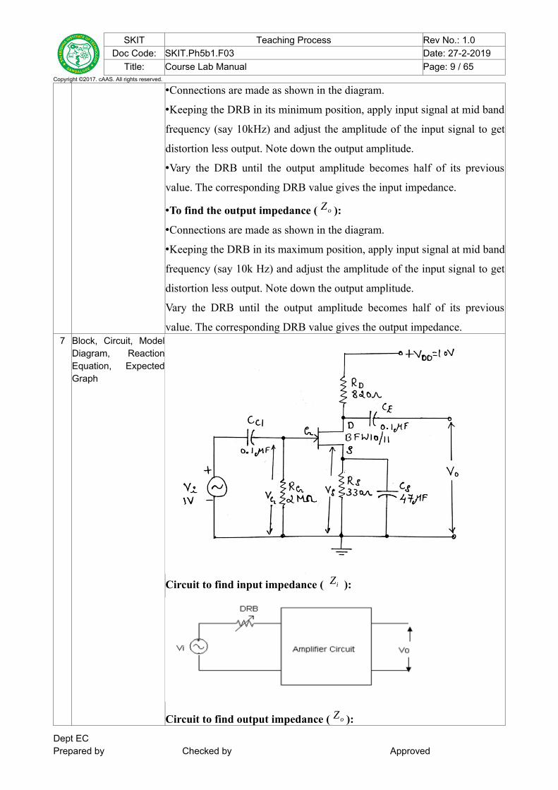
•Connections are made as shown in the diagram.
•Keeping the DRB in its minimum position, apply input signal at mid band
frequency (say 10kHz) and adjust the amplitude of the input signal to get
distortion less output. Note down the output amplitude.
•Vary the DRB until the output amplitude becomes half of its previous
value. The corresponding DRB value gives the input impedance.
•To find the output impedance ( Zo ):
•Connections are made as shown in the diagram.
•Keeping the DRB in its maximum position, apply input signal at mid band
frequency (say 10k Hz) and adjust the amplitude of the input signal to get
distortion less output. Note down the output amplitude.
Vary the DRB until the output amplitude becomes half of its previous
value. The corresponding DRB value gives the output impedance.7 Block, Circuit, Model
Diagram, ReactionEquation, ExpectedGraph
Circuit to find input impedance ( Zi ):
Circuit to find output impedance ( Zo ):
Dept ECPrepared by Checked by Approved
SKIT Teaching Process Rev No.: 1.0Doc Code: SKIT.Ph5b1.F03 Date: 27-2-2019
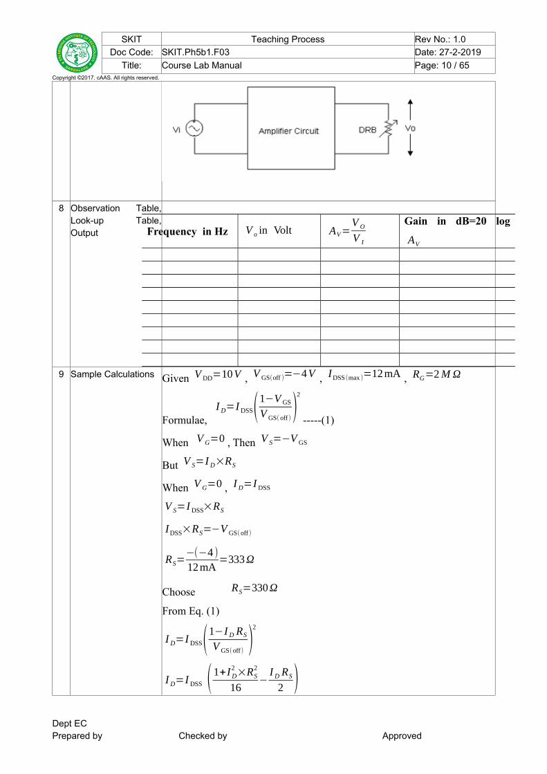
Title: Course Lab Manual Page: 10 / 65Copyright ©2017. cAAS. All rights reserved.
8 Observation Table,Look-up Table,Output
Frequency in Hz V o in Volt AV=V O
V I
Gain in dB=20 log
AV
9 Sample Calculations Given V DD=10V , V GS(off )=−4V , IDSS (max )=12mA , RG=2 M Ω
Formulae, I D=I DSS(1−V GS
V GS(off ))2
-----(1)
When V G=0 , Then V S=−V GS
But V S=I D×RS
When V G=0 , I D=I DSS
V S=I DSS×RS
IDSS×RS=−V GS(off )
RS=−(−4 )12mA
=333 Ω
Choose RS=330 Ω
From Eq. (1)
I D=I DSS(1−I D RS
V GS(off ) )2
I D=I DSS (1+I D2 ×RS
2
16−
I D RS
2 )Dept ECPrepared by Checked by Approved

SKIT Teaching Process Rev No.: 1.0Doc Code: SKIT.Ph5b1.F03 Date: 27-2-2019
Title: Course Lab Manual Page: 11 / 65Copyright ©2017. cAAS. All rights reserved.
I D=12×10−3 (1+ I D2 ×3302
16−
I D×330
2 )81.675 I D
2 −2.98 I D+12×10−3=0
I D=4 .6 mA or I D=31. 9 mA
Since I D cannot be greater than IDSS , Choose I D=4 .6 mA
Assume V DS=50%V DD , V DS=5 V
Applying KVL to output circuit
V DD=I D RD+V DS+ I D RS
V DD−V DS=I D( RD+RS)
10V−5VI D
=( RD+RS)
5V4 .6mA
=(RD+RS )
RD= 5V4 .6 mA
−330 Ω
RD=756 Ω
Choose RD=820 Ω
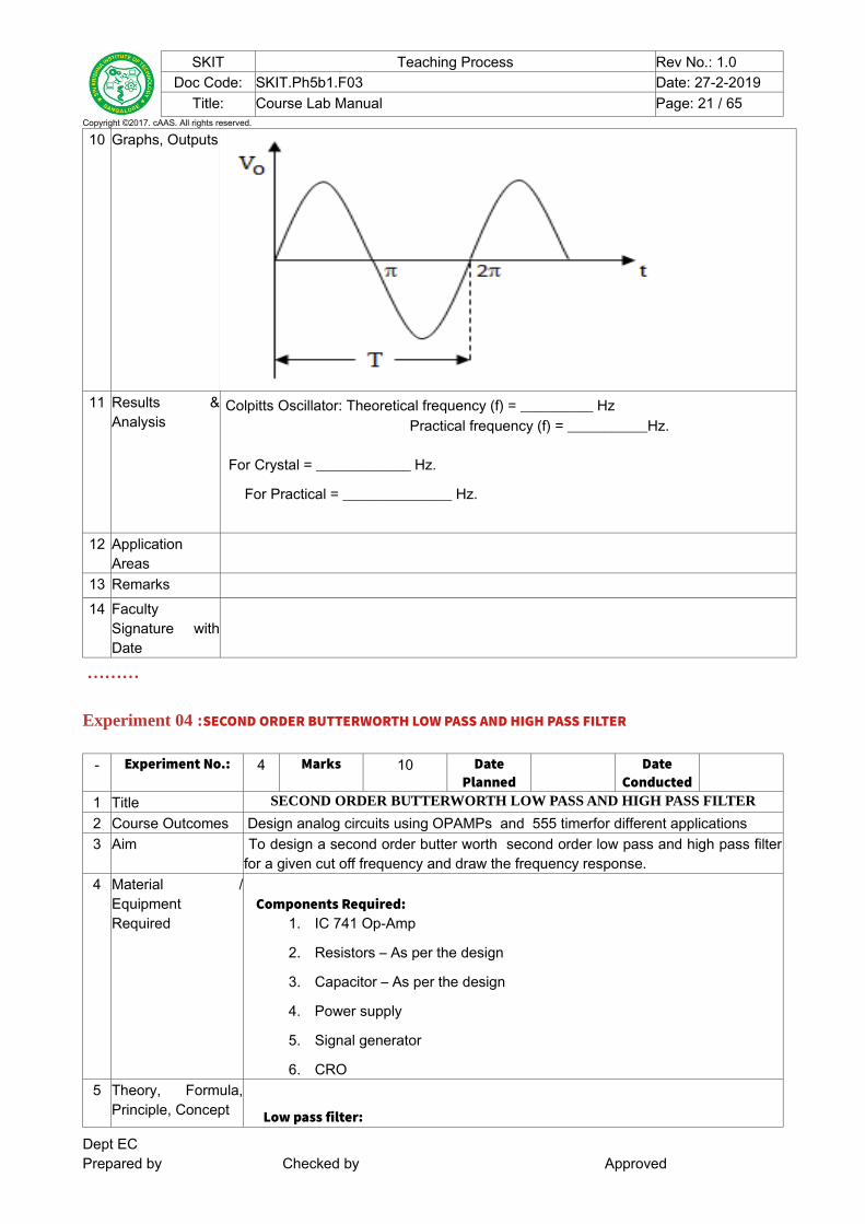
10 Graphs, Outputs
11 Results & Analysis 1. Quiescent point: V DS = _______V and I D = ________mA.
2. Voltage Gain ( AV ) = __________ ( in mid band region).
3. Bandwidth (BW) = ___________ Hz.
4. figure of merit (FM) = ____________ Hz.
5. Input impedance ( Zi ) = ____________, Output Impedance ( Zo )Dept ECPrepared by Checked by Approved

SKIT Teaching Process Rev No.: 1.0Doc Code: SKIT.Ph5b1.F03 Date: 27-2-2019
Title: Course Lab Manual Page: 12 / 65Copyright ©2017. cAAS. All rights reserved.
= __________12 Application Areas Used in CRO
used in electronic voltmeter13 Remarks14 Faculty Signature with
Date
Experiment 02 : BJT COMMON EMITTER AMPLIFIER
- Experiment No.: 2 Marks 10 DatePlanned
DateConducted
1 Title BJT COMMON EMITTER AMPLIFIER2 Course
OutcomesDesign analog circuits using BJT/FETs and evaluate their performance characteristics.
3 Aim To design and set up the BJT common emitter amplifier using voltage divider bias with
and without feedback and determine the gain- bandwidth product from its frequency
response.4 Material /
EquipmentRequired
Sl.
No.Particulars Range Quantity
1. Transistor (SL100/CL100) - 12. Resistor 47KΩ, 1.8KΩ,8.2KΩ,470Ω 1,1,1,13. Capacitor 0.47μF, 47μF 2,14. Signal Generator 20MHz 15. CRO - 16. Power Supply 0-30V 17. Multimeter - 18. Spring Board - 19. Connecting Wires - -
5 Theory,Formula,Principle,Concept
The single staged common emitter amplifier circuit uses voltage divider biasing.
This type of biasing arrangement uses two resistors as a potential divider network across
the supply with their centre point supplying the required base bias voltage to the transistor.
Voltage divider biasing is commonly used in the design of bipolar transistor amplifier circuits.
In common emitter amplifier circuits, capacitors C1 and C2 are used as coupling
capacitors to separate the AC signals from the DC biasing voltage. This ensures that the
biasing condition set up for the circuit to operate correctly is not affected by any additional
amplifier stages as the capacitors will only pass AC signals and block any DC component.
The output AC signal is then superimposed on the biasing of the following stages. Also a
bypass capacitor CE is included in the emitter leg circuit.
Dept ECPrepared by Checked by Approved

SKIT Teaching Process Rev No.: 1.0Doc Code: SKIT.Ph5b1.F03 Date: 27-2-2019
Title: Course Lab Manual Page: 13 / 65Copyright ©2017. cAAS. All rights reserved.
6 Procedure,Program,Activity,Algorithm,Pseudo Code
Check all the components and equipments for their good working condition.
Connections are made as shown in the circuit diagram.
By keeping the voltage knobs in minimum position and current knob in
maximum position switch on the power supply.
By disconnecting the AC source measure the quiescent point.
To find frequency response:
1. Connect the AC source. Keeping the frequency of the Ac source in mid band
region (say 10 kHz) adjust the amplitude to get the distortion less output. Note
down the amplitude of the input signal.
2. Keeping the input amplitude constant, Vary the frequency in suitable steps and
note down the corresponding output amplitude.
3. Calculate AV and gain in decibels. Plot a graph of frequency Vs gain in dB.
From the graph calculate f L , f H and band width.
4. Calculate figure of merit.
To find the input impedance (Zi ):
1. Connections are made as shown in the diagram.
2. Keeping the DRB in its minimum position, apply input signal at mid band
frequency (say 10kHz) and adjust the amplitude of the input signal to get
distortion less output. Note down the output amplitude.
3. Vary the DRB until the output amplitude becomes half of its previous value.
The corresponding DRB value gives the input impedance.
To find the output impedance (ZO ):
1. Connections are made as shown in the diagram.
2. Keeping the DRB in its maximum position, apply input signal at mid band
frequency (say 10k Hz) and adjust the amplitude of the input signal to get
distortion less output. Note down the output amplitude.
3. Vary the DRB until the output amplitude becomes half of its previous value.
The corresponding DRB value gives the output impedance.
Result:
Dept ECPrepared by Checked by Approved
SKIT Teaching Process Rev No.: 1.0Doc Code: SKIT.Ph5b1.F03 Date: 27-2-2019
Title: Course Lab Manual Page: 14 / 65Copyright ©2017. cAAS. All rights reserved.
1. Quiescent point: ¿¿¿
V CE=¿V , ¿¿¿
I C=¿mA.
2. Voltage Gain (AV ) = __________ (in mid band region).
3. Bandwidth (BW) = ___________ Hz.
4. Figure of merit (FM) = ____________ Hz.
5. Input impedance (Zi) = ____________, Output Impedance (ZO) =
__________.
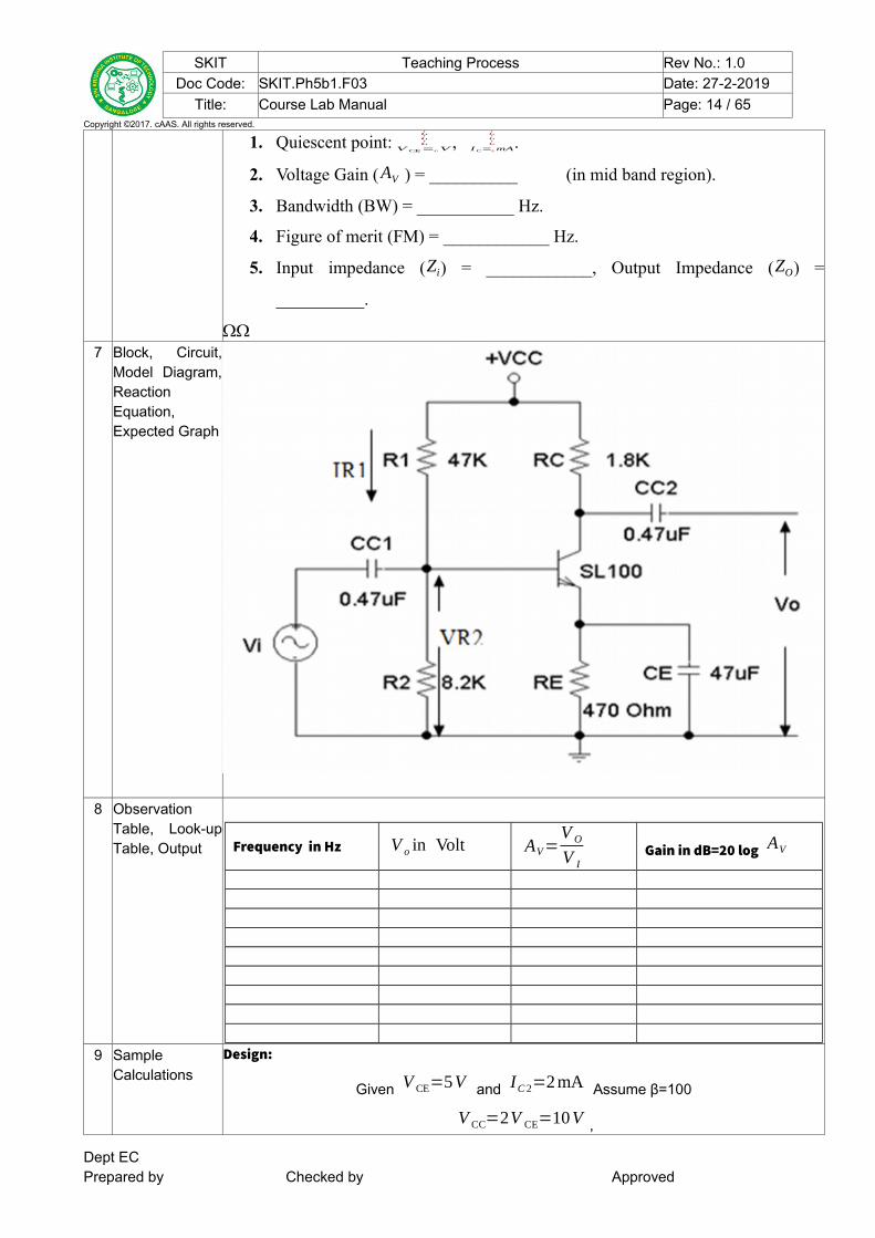
7 Block, Circuit,
Model Diagram,ReactionEquation,Expected Graph
8 Observation
Table, Look-upTable, Output
Frequency in Hz V o in Volt AV=V O
V IGain in dB=20 log AV
9 SampleCalculations
Design:
Given V CE=5V and IC 2=2mA Assume β=100
V CC=2V CE=10V ,
Dept ECPrepared by Checked by Approved

SKIT Teaching Process Rev No.: 1.0Doc Code: SKIT.Ph5b1.F03 Date: 27-2-2019
Title: Course Lab Manual Page: 15 / 65Copyright ©2017. cAAS. All rights reserved.
Let V RE=10%V CC=1V
RE=V RE
IC+ IB
I B=IC
β=2mA
100=20 μ A
RE=1
2mA+20μ A=495 Ω
Choose RE=470 Ω
Apply KVL to Collector Loop
V CC−IC RC−V CE−¿V E=0¿
RC=V CC−V CE−¿V E
IC
=10−5−12m
¿
RC=2 K Ω Choose RC=1. 8 KΩ
Let IR1=10 IB=10×20μ A=200 μ A
V R2=V BE+V E=0 .6+1=1 .6 V (Since transistor is silicon make V BE = 0.6 V)
R2=V R 2
IR1−IB= 1 .6V
200 μ+20μ=7 .2 K Ω
Choose R2=8 .2 KΩ
R1=V CC−V R 2
IR1
=10−1.6200 μ A
=42K Ω
Choose R1=47 KΩ
The condition is that XCE << RE
Let XCE=
RE
10
12 π f CE
= 47010
Let f=100Hz
CE=33 μ F
Choose CE=47 μ F
Also CC 1=CC 2=0 .47μF
Dept ECPrepared by Checked by Approved

SKIT Teaching Process Rev No.: 1.0Doc Code: SKIT.Ph5b1.F03 Date: 27-2-2019
Title: Course Lab Manual Page: 16 / 65Copyright ©2017. cAAS. All rights reserved.
10 Graphs, Outputs
11 Results &Analysis
Quiescent point: V CE=¿¿¿ , IC=¿¿ ¿ .
1. Voltage Gain ( AV ) = __________ (in mid band region).
2. Bandwidth (BW) = ___________ Hz.
3. Figure of merit (FM) = ____________ Hz.
4. Input impedance ( Zi ) = ____________ , Output Impedance ( ZO ) = __________ .
12 ApplicationAreas
Used in low noise amplifiersused in radio frequencies transceiver circuits
13 Remarks14 Faculty
Signature withDate
Experiment 03 : COLPITTS OSCILLATOR AND CRYSTAL OSCILLATOR
- Experiment No.: 3 Marks 10 DatePlanned
DateConducted
1 Title COLPITTS OSCILLATOR AND CRYSTAL OSCILLATOR
2 CourseOutcomes
Design analog circuits using BJT/FETs and evaluate their performance characteristics.
3 Aim To Design and set-up the following tuned oscillator circuits using BJT, and determine
the frequency of oscillation.
(a) Colpitts Oscillator (b) Crystal Oscillator 4 Material /
EquipmentRequired
Sl. No. Particulars Range Quantity
1. Transistor (SL100/CL100) - 12. Crystal 2MHz 13. Resistor 47KΩ, 1.8KΩ,8.2KΩ,470Ω 1,1,1,14. Capacitor 0.47μF,47 μF 2,15. Decade Capacitance Box - 2
Dept ECPrepared by Checked by Approved
SKIT Teaching Process Rev No.: 1.0Doc Code: SKIT.Ph5b1.F03 Date: 27-2-2019
Title: Course Lab Manual Page: 17 / 65Copyright ©2017. cAAS. All rights reserved.
6. CRO - 17. Power Supply 0-30V 18. Multimeter - 19. Spring Board - 110. Connecting Wires - -CRYSTAL OSCILLATOR
Sl. No. Particulars Range Quantity1. Transistor (SL100/CL100) - 12. Crystal 2MHz 13. Resistor 47KΩ, 1.8KΩ,8.2KΩ,470Ω 1,1,1,14. Capacitor 0.47μF,47 μF 2,15. Decade Capacitance Box - 26. CRO - 17. Power Supply 0-30V 18. Multimeter - 19. Spring Board - 110. Connecting Wires - -
5 Theory,Formula,Principle,Concept
Colpitts Oscillator: A Colpitts oscillator is an electronic oscillator that uses a combinationof inductor and capacitor to produce an output of certain frequency. It consists of a gaindevice with its output connected to the input in a feedback loop consisting of a parallel LCcircuit.
The Colpitts oscillator uses a capacitance voltage divider network as its feedback
source. The two capacitors are connected across a single common inductor. The
advantage of this type of capacitance circuit configuration is that with less and mutual
inductance within the tank circuit, frequency stability of the oscillator is improved along
with more simple design.
CRYSTAL OSCILLATOR:
Crystal oscillators are used in order to get stable sinusoidal signals despite of variations
in temperature, humidity, transistor and circuit parameters. A piezo electric crystal is
used in this oscillator as resonant tank circuit. Crystal works under the principal of piezo-
electric effect. i.e., when an AC signal applied across the crystal, it vibrates at the
frequency of the applied voltage. Conversely if the crystal is forced to vibrate it will
generate an AC signal. Commonly used crystals are Quartz, Rochelle salt etc.
6 Procedure,Program,Activity,
1. Connections are made as shown in the diagram.
Dept ECPrepared by Checked by Approved

SKIT Teaching Process Rev No.: 1.0Doc Code: SKIT.Ph5b1.F03 Date: 27-2-2019
Title: Course Lab Manual Page: 18 / 65Copyright ©2017. cAAS. All rights reserved.
Algorithm,Pseudo Code
2. The quiescent point of the amplifier is verified for the designed value.
3. Observe the output waveform on CRO and measure the frequency.
4. Verify the output frequency with the theoretical frequency.
Crystal oscillator
5. Connections are made as shown in the diagram.
6. The quiescent point of the amplifier is verified for the designed value.
7. Observe the output wave form on CRO and measure the frequency.
8. Verify the frequency with the crystal frequency.
7 Block, Circuit,Model Diagram,ReactionEquation,Expected Graph
Crystal oscillator:
Dept ECPrepared by Checked by Approved

SKIT Teaching Process Rev No.: 1.0Doc Code: SKIT.Ph5b1.F03 Date: 27-2-2019
Title: Course Lab Manual Page: 19 / 65Copyright ©2017. cAAS. All rights reserved.
8 ObservationTable, Look-upTable, Output
9 SampleCalculations
Colpitts Oscillator tank circuit design:
Choose A=2, f o=100 KHz
f o=1
2 π √LCeq ------(c)
Ceq=L1+L2 --------(d)
Condition for oscillation
A β≥1
A=C1
C2 => C1=2 C2
Find Ceq from (d) and L from (c)
crystal oscillator:
Design:
Given, V CE=5 V and IC=2mA , Assume = 100
V CC=2V CE=2×5=10V
Let V RE=10%V CC=1 V
Dept ECPrepared by Checked by Approved

SKIT Teaching Process Rev No.: 1.0Doc Code: SKIT.Ph5b1.F03 Date: 27-2-2019
Title: Course Lab Manual Page: 20 / 65Copyright ©2017. cAAS. All rights reserved.
RE=V RE
IC+ IB
I B=IC
β=2mA
100=20 μ A
RE=1
2mA+20μ=495 Ω
Choose RE=470 Ω
Apply KVL to collector loop
V CC−IC RC−V CE−V E=0
RC=V CC−V CE−V E
IC
=10−5−12 m
RC=2KΩ Choose RC=1.8KΩ
Let IR1=10 I B=10×20 μA=200 μA
VR2=V BE+V E=0 .6+1=1.6V (Since transistor is silicon make V BE=0.6V )
R2=VR1
IR 1−I B
= 1 .6200μA+20 μA
R2 = 7.2 K Choose R2 = 8.2 K
R1=(V CC−VR2)
IR1
=(10−1.6 )200μA
R1=42KΩ Choose R1=47 KΩ
XCE≪ RE
XCE=RE
10
12πf CE
= 47010
Let f = 100 Hz
CE = 33 F Choose R1 = 47 F
Choose CC1 = CC2 = 0.47 F
Dept ECPrepared by Checked by Approved
SKIT Teaching Process Rev No.: 1.0Doc Code: SKIT.Ph5b1.F03 Date: 27-2-2019
Title: Course Lab Manual Page: 21 / 65Copyright ©2017. cAAS. All rights reserved.
10 Graphs, Outputs
11 Results &Analysis
Colpitts Oscillator: Theoretical frequency (f) = __________ Hz Practical frequency (f) = ___________Hz.
For Crystal = _____________ Hz.
For Practical = _______________ Hz.
12 ApplicationAreas
13 Remarks
14 FacultySignature withDate
………
Experiment 04 :SECOND ORDER BUTTERWORTH LOW PASS AND HIGH PASS FILTER
- Experiment No.: 4 Marks 10 DatePlanned
DateConducted
1 Title SECOND ORDER BUTTERWORTH LOW PASS AND HIGH PASS FILTER
2 Course Outcomes Design analog circuits using OPAMPs and 555 timerfor different applications 3 Aim To design a second order butter worth second order low pass and high pass filter
for a given cut off frequency and draw the frequency response.4 Material /
EquipmentRequired
Components Required:
1. IC 741 Op-Amp
2. Resistors – As per the design
3. Capacitor – As per the design
4. Power supply
5. Signal generator
6. CRO5 Theory, Formula,
Principle, Concept Low pass filter:
Dept ECPrepared by Checked by Approved

SKIT Teaching Process Rev No.: 1.0Doc Code: SKIT.Ph5b1.F03 Date: 27-2-2019
Title: Course Lab Manual Page: 22 / 65Copyright ©2017. cAAS. All rights reserved.
Low pass filter allows only low frequency signal to pass
through them. A low pass filter can be a combination of capacitance,
inductance or resistance to produce high attenuation above a specified
frequency & little or no attenuation below that frequency .The frequency at
which the transition occurs is called cut-off frequency.
A first order low pass Butterworth filter uses RC network for
filtering. The op-Amp is used in non-inverting configuration.
The first order filter can be connected to second order LPF by
using additional RC network as shown in fig1.
2nd order:
The stop-band response in 2nd order LPF is 40dB/decade. At low
frequency, both capacitors appear open and the circuit becomes a non-
inverting amplifier (. ‧ . XC=
12 πFC)
As frequency increase, the gain eventually starts to decrease until-
it is down 3dB at the cutoff frequency. As frequency increase the cut off
frequency, the o/p is attenuated.
b) High pass filter:
High pass filter passes high frequency signals to pass through it.
Again frequency sensitive components such as capacitors &
inductors are used in conjunction with the resistors.
The first order high pass filter is formed from first order low pass
filter by interchanging the R&C components &second order HPF
filter can be obtained from 2nd order LPF by interchanging R&C as
shown in Fig3.
Dept ECPrepared by Checked by Approved

SKIT Teaching Process Rev No.: 1.0Doc Code: SKIT.Ph5b1.F03 Date: 27-2-2019
Title: Course Lab Manual Page: 23 / 65Copyright ©2017. cAAS. All rights reserved.
Here as frequency increase, the capacitors act as short & the
circuit behaves as amplifier with gain Af but when the frequency is
low, the capacitor act as open circuit & hence very little signal passes
through the circuit.
6 Procedure,Program, Activity,Algorithm, PseudoCode
1. Rig up the circuits as show in the diagrams2. apply the input as specified3. vary the input signal frequency and note down the output voltagesand calculate the gain convert the gain in db4. plot the graph frequency/ gain in db and observe the cut-off pointsand calculate the roll off
7 Block, Circuit,Model Diagram,Reaction Equation,Expected Graph
a) High pass filter
Circuit Diagram:
Dept ECPrepared by Checked by Approved

SKIT Teaching Process Rev No.: 1.0Doc Code: SKIT.Ph5b1.F03 Date: 27-2-2019
Title: Course Lab Manual Page: 24 / 65Copyright ©2017. cAAS. All rights reserved.
8 Observation Table,
Look-up Table,Output
V i = 2V p−p
Frequency
( H Z )V O (V) AV =
V O
V I20 LOG AV
9 SampleCalculations
LPF: The higher cutoff frequency that is the frequency at which signal
falls (3dB) below is given by
for LPH: f H =
12π √R2 R3 C2 C3
HPF:
The lower cutoff frequency that is the frequency at which signal
strength falls 3dB below this is given by
Dept ECPrepared by Checked by Approved
SKIT Teaching Process Rev No.: 1.0Doc Code: SKIT.Ph5b1.F03 Date: 27-2-2019
Title: Course Lab Manual Page: 25 / 65Copyright ©2017. cAAS. All rights reserved.
fL =
12 π √R2 R3 C2 C3
b) Low pass filter
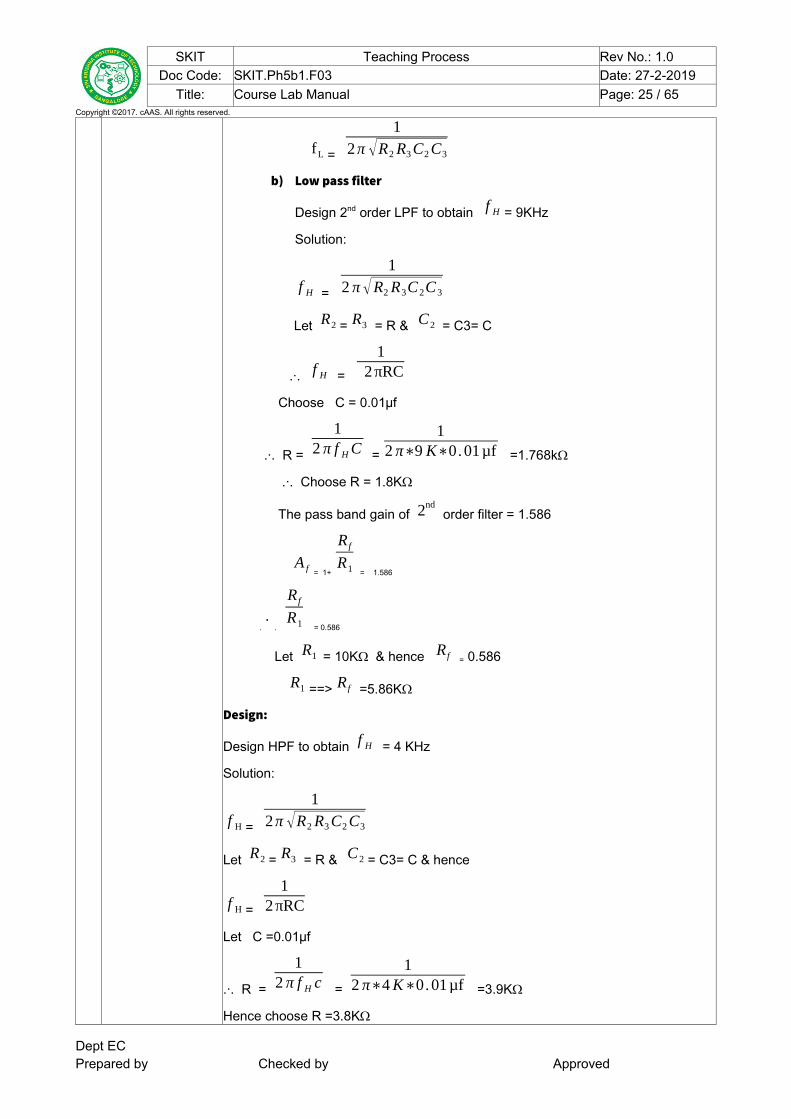
Design 2nd order LPF to obtain f H = 9KHz
Solution:
f H =
12 π √R2 R3C2C3
Let R2 = R3 = R & C2 = C3= C
.‧. f H =
1 2πRC
Choose C = 0.01µf
.‧. R =
12 π f H C =
12 π∗9 K∗0.01µf =1.768kΩ
.‧. Choose R = 1.8KΩ
The pass band gain of 2nd order filter = 1.586
A f = 1+
R f
R1 = 1.586
.‧
.
R f
R1 = 0.586
Let R1 = 10KΩ & hence R f = 0.586
R1 ==> R f =5.86KΩ
Design:
Design HPF to obtain f H = 4 KHz
Solution:
f H =
12 π √R2 R3 C2 C3
Let R2 = R3 = R & C2 = C3= C & hence
f H =
12πRC
Let C =0.01µf
.‧. R =
12 π f H c =
12 π∗4 K∗0.01µf =3.9KΩ
Hence choose R =3.8KΩ
Dept ECPrepared by Checked by Approved
SKIT Teaching Process Rev No.: 1.0Doc Code: SKIT.Ph5b1.F03 Date: 27-2-2019
Title: Course Lab Manual Page: 26 / 65Copyright ©2017. cAAS. All rights reserved.
The pass band gain of 2nd order filter is 1.586
.‧. A f = 1+
R f
R1 = 1.586
R f
R1 = 0.586
Let R1 =10KΩ & hence R f =0.586 R1 ==> R f = 5.8KΩ
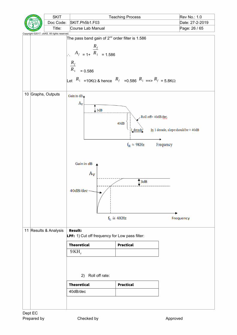
10 Graphs, Outputs
11 Results & Analysis Result:LPF: 1) Cut off frequency for Low pass filter:
Theoretical Practical
9 KHz
2) Roll off rate:
Theoretical Practical
40dB/dec
Dept ECPrepared by Checked by Approved

SKIT Teaching Process Rev No.: 1.0Doc Code: SKIT.Ph5b1.F03 Date: 27-2-2019
Title: Course Lab Manual Page: 27 / 65Copyright ©2017. cAAS. All rights reserved.
HPF: 1) Cut off frequency for HPF:
Theoretical Practical
4 KHz
2) Roll off rate:
Theoretical Practical
40dB/dec
12 Application Areas Used in generation of high frequencies sinusoidal signal used in computer , instrumentation and in digital systems
13 Remarks14 Faculty Signature
with Date
………
Experiment 05 : ADDER, INTEGRATOR AND DIFFERENTIATOR USING OP-AMP
- Experiment No.: 5 Marks 10 DatePlanned
DateConducted
1 Title ADDER, INTEGRATOR AND DIFFERENTIATOR USING OP-AMP2 Course Outcomes Design analog circuits using OPAMPs and 555 timerfor different applications 3 Aim To design adder, integrator and differentiator circuit for given specification using
Op-Amp.4 Material /
EquipmentRequired
1. IC 741 -Op-Amp
2. Resistors – as per the design
3. Capacitor – as per the design
4. Dc power supply
5. Signal generator
6. CRO
7. Digital multimeter/Voltmeter
5 Theory, Formula,Principle, Concept
Adder:The most common application of Op-Amp is the summing-amplifier (or
adder) circuit. Fig. 1 shows the inverting configuration of summing circuit with 2
inputs V 1 and V 2 . Depending on the relationship between R f , the feedback
resistor and the input resistor R1 and R2 , the circuit can be used as summing
Dept ECPrepared by Checked by Approved
SKIT Teaching Process Rev No.: 1.0Doc Code: SKIT.Ph5b1.F03 Date: 27-2-2019
Title: Course Lab Manual Page: 28 / 65Copyright ©2017. cAAS. All rights reserved.
amplifier, scaling amplifier or averaging Amplifier. The input expression for the
circuit can be written as (or obtained as)
I F=I1 + I2
−V o
Rf =
V 1
R1 +
V 2
R2
.‧. V o = - [
R f
R1 V 1 + [
R f
R2 V 2 ] ……… (1)
If R1=R2=R f=R in (1), then
V o = - (V 1 + V 2) ---- summing amplifier. Here , the o/p voltage is
equal to negative sum of all the inputs. Hence circuit act as summing
amplifier.
If R1 , R2 R f different , then the circuit is called scaling amplifier.
If R1=R2=R & if
R f
R = 12 , then the circuit can be used as an
averaging circuit.
2. Integrator:
A circuit in which the output voltage is the integral of the input
voltage is called integrator as shown in Fig2.
Relationship between voltage and current through capacitor is given by
ic = c
d V C
dt
Applying Kirchhoff’s law,
i1≃ if
.‧.
V in
R1 = CF
d (−V O)dt
.‧. V O = -
1R1 CF
∫0
tV in dt+const
As seen ,the o/p voltage is directly proportional to the negative of the input
voltage and inversely proportional to time constant R1 CF .
If V in =0, then input offset voltage and the capacitor CT produce error
Dept ECPrepared by Checked by Approved

SKIT Teaching Process Rev No.: 1.0Doc Code: SKIT.Ph5b1.F03 Date: 27-2-2019
Title: Course Lab Manual Page: 29 / 65Copyright ©2017. cAAS. All rights reserved.
voltage at output of integrator. To reduce the error voltages, resistor RF is
connected across the feedback capacitor CF .
Addition of RF improves stability and low frequency roll off problems and
hence minimizes the variations in the output voltage.
The input signal will be integrated properly if the time period T of the signal
is larger than or equal to RF CF .
.‧. T ≥ RF CF .
.
3. Differentiator:
Differentiator performs the mathematical operation of
differentiation. The output voltage can be expressed in Fig. 3 as
ic = iF
.‧. C1 . d (V in )
dt =-
V O
RF
. ‧ . V O = - RF CF
d(V in )dt
The gain
RF
XC1 increase with increase in frequency. Also, the input
impedance XC 1 decreases with increase in frequency which makes
circuit susceptible to high frequency noise.
The stability & high frequency noise problem can be corrected by two
components CF & R1 .
The input signal will be differentiated properly if the time period T of
the input signal is larger than or equal to RF C1 .
.‧. T ≥ RF C1 .
6 Procedure,Program, Activity,Algorithm, PseudoCode
Adder :1. Before wiring the circuit, check the components for its working .
2. Connect the circuit as shown in Fig.1.
3. Set the input voltages V 1 and V 2 and measure the output voltage V o
using multimeter.
4. Compare theoretical and practical output voltages Dept ECPrepared by Checked by Approved

SKIT Teaching Process Rev No.: 1.0Doc Code: SKIT.Ph5b1.F03 Date: 27-2-2019
Title: Course Lab Manual Page: 30 / 65Copyright ©2017. cAAS. All rights reserved.
5. Integrator Procedure:
6. Check all the components for its working.
7. Make the connections as shown in Fig.2.
8. Set the input voltage using signal generator to 4V (or 2V) peak to peak
square wave at 1KHz frequency.
9. Observe the input & output signals of circuit on CRO.
10. Sketch the output for RC = 10T & RC =T & RC = 0.1T.
Differentiator”
11. Check all the components for its working.
12. Make the circuit diagram as show in Fig.3.
13. Set the input voltage using signal generator to 4V (or 2V) peak to peak
triangular wave at 1KHz frequency.
14. Sketch the output for RC= 10T, 0.025T & varying R.
15. Observe the output signal on CRO
7 Block, Circuit,Model Diagram,Reaction Equation,Expected Graph
Adder circuit
:
Integrator:
Dept ECPrepared by Checked by Approved

SKIT Teaching Process Rev No.: 1.0Doc Code: SKIT.Ph5b1.F03 Date: 27-2-2019
Title: Course Lab Manual Page: 31 / 65Copyright ©2017. cAAS. All rights reserved.
Differentiator:
8 Observation Table,Look-up Table,Output
Input voltage (V) Output voltage ( vo )
V 1 V 2 Theoretical V O Practical V O
9 SampleCalculations
ADDER Design:Design a circuit to obtain the output voltage
V O = - (5V 1+3V 2)
Solution:
Given V O = - (5V 1+3V 2)
But V O =- [
R f
R1 V 1 +
R f
R2 V 2 ] Dept ECPrepared by Checked by Approved

SKIT Teaching Process Rev No.: 1.0Doc Code: SKIT.Ph5b1.F03 Date: 27-2-2019
Title: Course Lab Manual Page: 32 / 65Copyright ©2017. cAAS. All rights reserved.
Given
R f
R1 =5 &
R f
R2 = 3
.‧. R f = 5 R1 , R f = 3 R2
Choose R f =10 KΩ
.‧. R1 =
R f
5 =
10k5 = 2KΩ ………. R1 = 2KΩ
R2 =
R f
3 =
10k3 = 3.3KΩ ………. R2 = 3.3KΩ
Integrator Design:
Given T = 1ms
a) Let RC =10T
Choose C=0.1µf
.‧. R =
10TC =
10∗1∗10−3
0.1∗10−6
R =100kΩ
b) If RC = T
.‧. R =
TC =
1∗10−3
0 .1∗10−6
.‧. R =10KΩ
c) If RC =0.1 T
R =
0 .1∗1∗10−3
0 .1∗10−6
R = 1KΩ
Differentor Design:
Given T = 1ms
a) Let RC =10T
Choose C =0.1µf
.‧. R = 10T
C =
10∗1∗10−¿3
0. 1∗10−6 ¿
R = 100kΩ
b) If RC =0.025T
R =
0 .025TC =
0 .025∗1∗10−3
0 .1∗10−6
R = 250Ω
Dept ECPrepared by Checked by Approved
SKIT Teaching Process Rev No.: 1.0Doc Code: SKIT.Ph5b1.F03 Date: 27-2-2019
Title: Course Lab Manual Page: 33 / 65Copyright ©2017. cAAS. All rights reserved.
c) If RC =T
R =
TC =
1∗10−3
0 .1∗10−6
R = 10KΩ
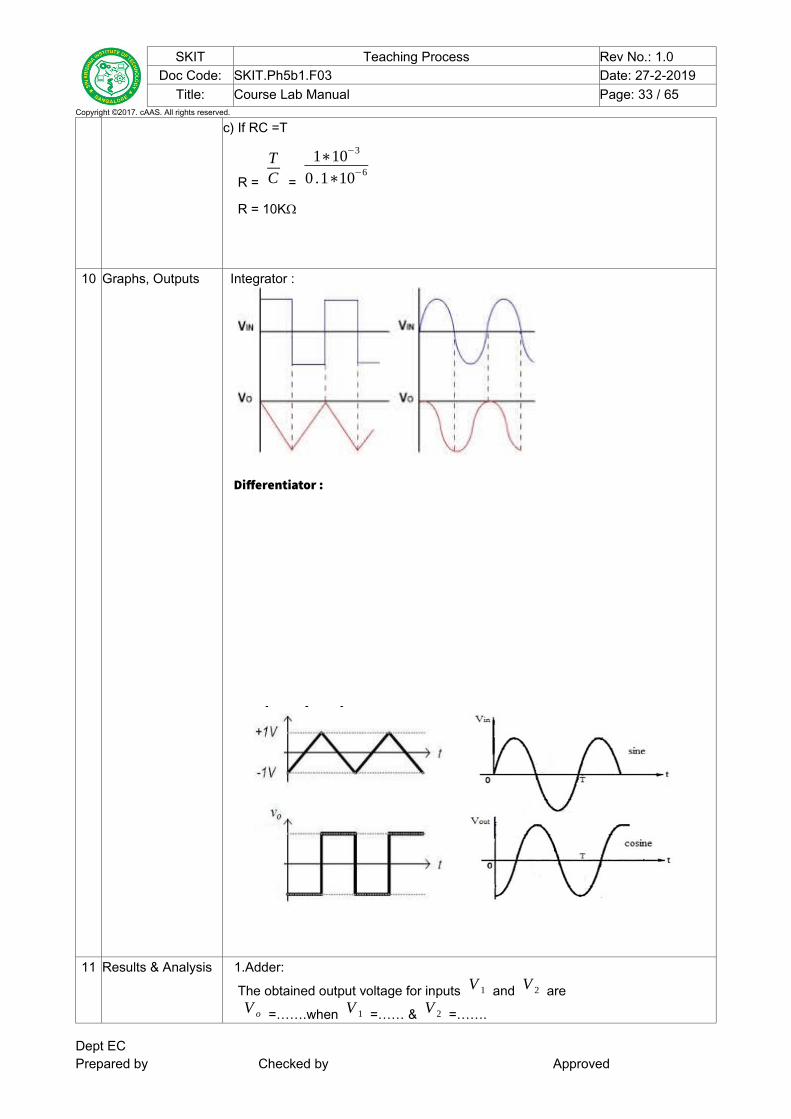
10 Graphs, Outputs Integrator :
Differentiator :
11 Results & Analysis 1.Adder:
The obtained output voltage for inputs V 1 and V 2 are
V o =…….when V 1 =…… & V 2 =…….
Dept ECPrepared by Checked by Approved

SKIT Teaching Process Rev No.: 1.0Doc Code: SKIT.Ph5b1.F03 Date: 27-2-2019
Title: Course Lab Manual Page: 34 / 65Copyright ©2017. cAAS. All rights reserved.
2. The operation of integrator circuit is verified.
3. Operation of differentiator circuit is verified.
12 Application Areas The adder circuit is commonly used in
1). Analog computers
2). Audio mixers in which no of inputs are added or mixed to produce
desired output.
Integrator is commonly used in
1. Analog computers.
2. Analog to digital converter.
3. Signal wave shaping circuits
Differentiator is commonly used in
1. Wave shaping circuits to detect high frequency component in input
signal.
2. Rate of change detector in FM modulators.13 Remarks14 Faculty Signature
with Date
Experiment 06 : SCHMITT TRIGGER
- Experiment No.: 6 Marks 10 DatePlanned
DateConducted
1 Title SCHMITT TRIGGER2 Course Outcomes Design analog circuits using OPAMPs and 555 timerfor different applications 3 Aim Design and Testing of Schmitt trigger circuit for different hysteresis value4 Material /
EquipmentRequired
IC trainer, signal generator, CRO. Resisters, OP AMP, Patch Chords, Digital multimeter.
5 Theory, Formula,Principle, Concept
A Schmitt trigger is a comparator circuit with hysteresis implemented by applyingpositive feedback to the non inverting input of a comparator or differential amplifier.It is an active circuit which converts an analog input signal to a digital output signal. In the non-inverting configuration, when the input is higher than a chosenthreshold, the output is high. When the input is below a different (lower) chosenthreshold the output is low, and when the input is between the two levels the outputretains its value. This dual threshold action is called hysteresis and implies that theSchmitt trigger possesses memory and can act as a bistable multivibrator.
Schmitt trigger devices are typically used in signal conditioning applications
to remove noise from signals used in digital circuits, particularly mechanical contact
bounce. They are also used in closed loop negative feedback configurations toDept ECPrepared by Checked by Approved

SKIT Teaching Process Rev No.: 1.0Doc Code: SKIT.Ph5b1.F03 Date: 27-2-2019
Title: Course Lab Manual Page: 35 / 65Copyright ©2017. cAAS. All rights reserved.
implement relaxation oscillators, used in function generators and switching power
supplies.
Test a Comparator circuit
An inverting 741 IC op-amp comparator circuit is shown in the figure below.
It is called an inverting comparator circuit as the sinusoidal input signal Vin is
applied to the inverting terminal. The fixed reference voltage Vref is give to the non-
inverting terminal (+) of the op-amp. A potentiometer is used as a voltage divider
circuit to obtain the reference voltage in the non-inverting input terminal. Bothe
ends of the POT are connected to the dc supply voltage +VCC and -VEE. The
wiper is connected to the non-inverting input terminal. When the wiper is rotated to
a value near +VCC, Vref becomes more positive, and when the wiper is rotated
towards -VEE, the value of Vref becomes more negative. The waveforms are
shown below.
Inverting Comparator circuit
Dept ECPrepared by Checked by Approved
SKIT Teaching Process Rev No.: 1.0Doc Code: SKIT.Ph5b1.F03 Date: 27-2-2019
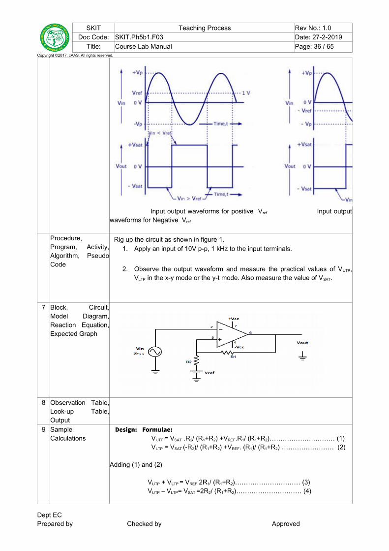
Title: Course Lab Manual Page: 36 / 65Copyright ©2017. cAAS. All rights reserved.
Input output waveforms for positive Vref Input outputwaveforms for Negative Vref
Procedure,Program, Activity,Algorithm, PseudoCode
Rig up the circuit as shown in figure 1.1. Apply an input of 10V p-p, 1 kHz to the input terminals.
2. Observe the output waveform and measure the practical values of VUTP,VLTP in the x-y mode or the y-t mode. Also measure the value of VSAT.
7 Block, Circuit,Model Diagram,Reaction Equation,Expected Graph
8 Observation Table,
Look-up Table,Output
9 SampleCalculations
Design: Formulae: VUTP = VSAT .R2/ (R1+R2) +VREF.R1/ (R1+R2)………………………… (1) VLTP = VSAT (-R2)/ (R1+R2) +VREF. (R1)/ (R1+R2) …………………… (2)
Adding (1) and (2)
VUTP + VLTP = VREF 2R1/ (R1+R2)………………………… (3) VUTP – VLTP= VSAT =2R2/ (R1+R2)………………………… (4)
Dept ECPrepared by Checked by Approved

SKIT Teaching Process Rev No.: 1.0Doc Code: SKIT.Ph5b1.F03 Date: 27-2-2019
Title: Course Lab Manual Page: 37 / 65Copyright ©2017. cAAS. All rights reserved.
VUTP = 4V, VLTP =2V, VSAT=12VFrom (4) R2/ (R1+R2) = 0.08333 Therefore R1/R2 =11Choose R2 =1 k ohm, R1 = 11 k ohmFrom (3)VREF = (VUTP + VLTP). (R1+R2) / (2 R1), VREF = (6. 12 x 103)/ (2. 11 x 103)VREF = 3.272V
10 Graphs, Outputs
11 Results & Analysis VUTP (Practical) = ……………………………………..Volts. VLTP (Practical) = ……………………………………..Volts.V+sat =……………………………………..Volts.V-sat =……………………………………..Volts.
12 Application Areas Used in signal conditioning to remove noise
13 Remarks14 Faculty Signature
with Date
Experiment 07 : R-2R DAC USING OP-AMP
- Experiment No.: 8 Marks 10 DatePlanned
DateConducted
1 Title R-2R DAC USING OP-AMP2 Course Outcomes Design analog circuits using OPAMPs and 555 timerfor different applications 3 Aim .1. To design 4 bit R-2R digital to analog convertor using Op-Amp and verify its
operation using input toggle switch.2. To generate staircase waveform using mod-16 counter.
4 Material /EquipmentRequired
Components Required: 1. IC 741 Op-Amp
2. Resistors –As per the design
3. Dc power supply
4. IC trainer kit
Dept ECPrepared by Checked by Approved
SKIT Teaching Process Rev No.: 1.0Doc Code: SKIT.Ph5b1.F03 Date: 27-2-2019
Title: Course Lab Manual Page: 38 / 65Copyright ©2017. cAAS. All rights reserved.
5. CRO
6. Millimeter / Voltmeter
7. IC7493 or equivalent
5 Theory, Formula,Principle, Concept
R-2R DAC is shown in Fig. 1. It consists of only two resistors R and 2R forming
ladder network and an Op-Amp acting as voltage follower. Here Do , D1 , D2 & D3
are digital inputs which are controlled by the Switches S0 , S1 , S2 , & S3 .When the digital input is ‘1’, then the corresponding switch connects the resistor
2R to V ref and when digital input is ‘0’, then the switch connects the resistor 2R
to the ground line. Since the ladder is composed of linear resistors, it is a linear
network and hence principle of superposition can be used to obtain the output
voltage.
The analog output voltage V o for 4 bit DAC can be written as
V o = [23 D3+22 D2+21 D1+20 D0+¿¿ ] V 1 where
V 1 = [ V ref
2N
] *[
2RR+2 R
]= V ref
2N
[
2 R3 R ] =
V ref
2N
[
23 ]
Since N=4 [4 bit DAC], V 1 becomes
V 1 =
V r e f
24
*
23
V 1 =
V ref
24
.‧. V o = [ 8 D3+4 D2+2 D1+D0 ]* V ref
24
6 Procedure,Program, Activity,Algorithm, PseudoCode
1. Verify the components for its working.
2. Make the connection as shown in Fig.1.
3. For different digital inputs, measure the output voltage using multimeter.
4 Verify whether the theoretical values is matching with practical values & plot thegraph of input V/s output. Procedure:1. Check the components for its working.
2. Make connection as shown in Fig. 3.
3. Construct modulo16 counter using suitable IC like 7493 or 74193.
Dept ECPrepared by Checked by Approved
SKIT Teaching Process Rev No.: 1.0Doc Code: SKIT.Ph5b1.F03 Date: 27-2-2019
Title: Course Lab Manual Page: 39 / 65Copyright ©2017. cAAS. All rights reserved.
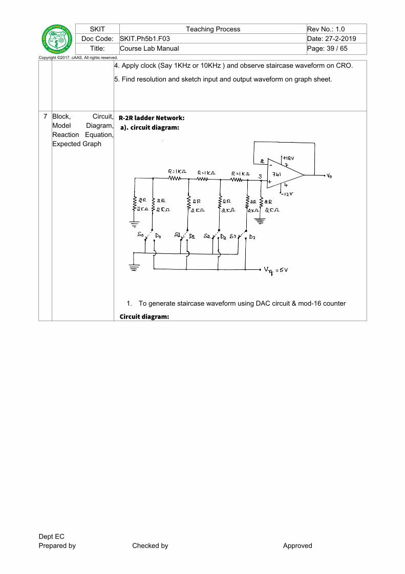
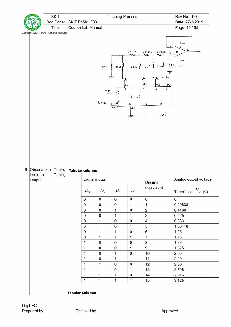
4. Apply clock (Say 1KHz or 10KHz ) and observe staircase waveform on CRO.
5. Find resolution and sketch input and output waveform on graph sheet.
7 Block, Circuit,Model Diagram,Reaction Equation,Expected Graph
R-2R ladder Network:a). circuit diagram:
1. To generate staircase waveform using DAC circuit & mod-16 counter
Circuit diagram:
Dept ECPrepared by Checked by Approved
SKIT Teaching Process Rev No.: 1.0Doc Code: SKIT.Ph5b1.F03 Date: 27-2-2019
Title: Course Lab Manual Page: 40 / 65Copyright ©2017. cAAS. All rights reserved.
8 Observation Table,Look-up Table,Output
Tabular column:
Digital inputsDecimalequivalent
Analog output voltage
D3 D2 D1 D0 Theoretical V 0 (V)
0 0 0 0 0 00 0 0 1 1 0.208330 0 1 0 2 0.41660 0 1 1 3 0.6250 1 0 0 4 0.8330 1 0 1 5 1.004160 1 1 0 6 1.250 1 1 1 7 1.451 0 0 0 8 1.661 0 0 1 9 1.8751 0 1 0 10 2.051 0 1 1 11 2.291 1 0 0 12 2.501 1 0 1 13 2.7081 1 1 0 14 2.9161 1 1 1 15 3.125
Tabular Column:
Dept ECPrepared by Checked by Approved

SKIT Teaching Process Rev No.: 1.0Doc Code: SKIT.Ph5b1.F03 Date: 27-2-2019
Title: Course Lab Manual Page: 41 / 65Copyright ©2017. cAAS. All rights reserved.
Step width Resolution
Ideal Obtained Ideal Obtained
% Resolution =
StepsizeFull scale *100
=
Stepwidth4 *100
9 SampleCalculations
Given: No of steps =15Solution:
w.k.t, No of steps = 2N−¿¿ 1
15 = 2N−¿¿ 1
14 = 2N
Apply log2 on both sides
log214 = log2 2N
log214 =N
log 14 log 2 = N
N = 3.8
.‧. Resolution = N
Use 4 bit DAC with minimum step size as 0.208V.
This is a 4 bit R-2R ladder N/W shown in Fig3.
a) Given :N=4 and step size =0.5V
Solution:
Minimum step size =
V ref
24 =
524 = 0.208V
Given step = 0.5V
.‧. Maximum o/p voltage = V omax = step size * No of steps
= 0.5 * ( 24-1)
= 0.5 * 15
= 7.5V
Given steps =0.5
Dept ECPrepared by Checked by Approved
SKIT Teaching Process Rev No.: 1.0Doc Code: SKIT.Ph5b1.F03 Date: 27-2-2019
Title: Course Lab Manual Page: 42 / 65Copyright ©2017. cAAS. All rights reserved.
.‧. Gain = A f =
Given stepminimum step =
0 .5
0 .208 = 2.4V
But A f = 1+
R f
R1
2.4 = 1+
R f
R1
.‧.
R f
R1 =1.4
.‧. R f =1.4 R1
Let R1 =10KΩ
.‧. R f =1.4*10KΩ
= 14KΩ
R f ≈15KΩ
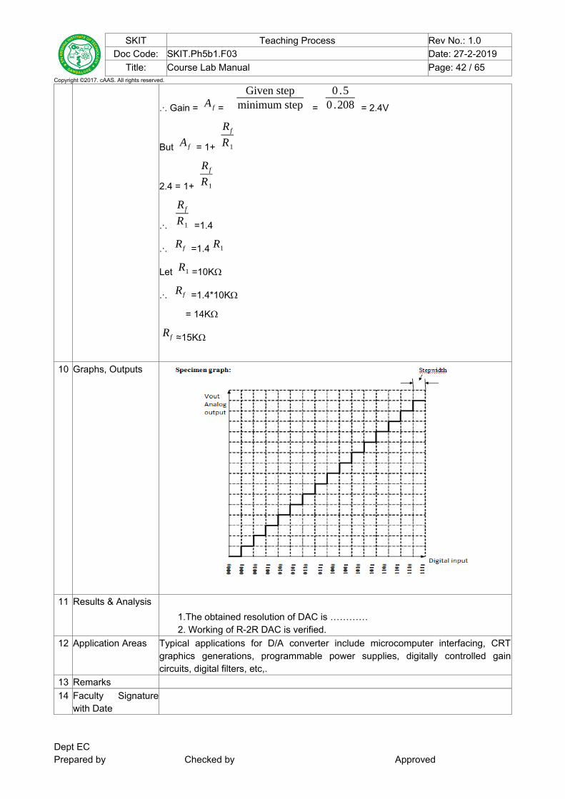
10 Graphs, Outputs
11 Results & Analysis 1.The obtained resolution of DAC is ………… 2. Working of R-2R DAC is verified.
12 Application Areas Typical applications for D/A converter include microcomputer interfacing, CRTgraphics generations, programmable power supplies, digitally controlled gaincircuits, digital filters, etc,.
13 Remarks14 Faculty Signature
with Date
Dept ECPrepared by Checked by Approved

SKIT Teaching Process Rev No.: 1.0Doc Code: SKIT.Ph5b1.F03 Date: 27-2-2019
Title: Course Lab Manual Page: 43 / 65Copyright ©2017. cAAS. All rights reserved.
Experiment 08 : ASTABLE AND MONOSTABLE MULTIVIBRATOR USING IC 555
- Experiment No.: 8 Marks 10 DatePlanned
DateConducted
1 Title ASTABLE AND MONOSTABLE MULTIVIBRATOR USING IC 5552 Course Outcomes Design analog circuits using OPAMPs and 555 timerfor different applications 3 Aim 1.Design Astable multi-vibrator using IC 555 timer to generator a clock frequency
of 1KHz with 0.75 duty cycle (unsymmetrical) and 0.5 duty cycle (symmetrical).2. Design monostable multi-vibrator using IC 555 timer.
4 Material /EquipmentRequired
1. 555timer
2. Resistors – As per the design
3. Capacitors – As per the design
4. Power supply
5. Diode – 1N4001
6. Signal generator 5 Theory, Formula,
Principle, Concept Astable multivibrator:
An astable multi-vibrator, often called a free running multi-vibrator
is a rectangular wave generating circuit. The circuit does not require any
external trigger to change the output & hence the name free running. The time
during which the output is either high or low is determined by the two resistors
& capacitors which are connected externally.
Fig.1 shows the 555 timer connected as an astable multivibrator. To
understand the circuit operations consider the internal block diagram of the
555 timer.
Initially when output is high, capacitor C starts towards V CC through
RA and RB . However, as soon as voltage across the capacitor equals
23
V CC , comparator -1 triggers the flip-flop and the o/p switches low. Now
capacitor C starts discharging through RB and transistor Q1 . When the
voltage across C equals 13 V CC , comparators output triggers the flip-flop
and output goes to high. Then the cycle repeats the output voltage and
Dept ECPrepared by Checked by Approved

SKIT Teaching Process Rev No.: 1.0Doc Code: SKIT.Ph5b1.F03 Date: 27-2-2019
Title: Course Lab Manual Page: 44 / 65Copyright ©2017. cAAS. All rights reserved.
capacitor voltage waveform as shown in Fig. 2.
The time during which the capacitor charges from
13 V CC to
23 V CC is
equal to the time the output is high & is given by
tC = 0.69( RA + RB .) C
The time during which, the capacitor discharges from
23 V CC to
13 V CC is
equal to the time the output is low & is given by
td = 0.69( RB ) C
.‧. Total period T = tC + td
= 0.69( RA + RB ) C
Hence frequency of oscillator is f o =
1T =
1 . 45( RA+2 RB)C
The duty cycle is the ratio of time tC during which the output is high to the total
period T.
% duty cycle =
tC
T *100
=
RA+RB
RA+2 RB * 100%
As seen from above equation, astable multi-vibrator will not produce square
wave unless the resistance RA =0. With RA =0, pin 7 is directly connected to
Dept ECPrepared by Checked by Approved

SKIT Teaching Process Rev No.: 1.0Doc Code: SKIT.Ph5b1.F03 Date: 27-2-2019
Title: Course Lab Manual Page: 45 / 65Copyright ©2017. cAAS. All rights reserved.
V CC & when capacitor discharge through RB , an extra current is supplied to Q1
by V CC through short between 7 & V CC which damages Q1 & hence timer.
Without reducing RA to 0Ω, the astable multi-vibrator can produce square
wave output simply by connecting diode across RB as shown in Fig.3.
2. Monostable multivibrator:
A monostable multi-vibrator is often called as one shot
multi-vibrator. It is a pulse generating circuit in which the duration of the pulse is
determined by the RC network connected externally. When an external trigger
pulse is applied, the output is forced to go high. The time the output remains high is
determined by the external RC network connected to the timer. At the end of time
interval, the output automatically reverse back to its logic low stable states. The
output stays low until the trigger pulse is again applied. Then the cycle repeats. The
monostable circuit has only one stable state & hence the name monostable.
Circuit operation:
The circuit is shown in Fig. 5. Initially, when the output is low,
transistor Q1 is on & capacitor C is shorted to ground. However, upon the
application of negative trigger pulse to pin 2, transistor Q1 is turned off, which
releases the short circuit across the external capacitor C & drives the output
high.The capacitor C now starts charging up towards V CC through RA .
However,when the voltage across the capacitor equals
23 V CC , comparator 1
output switch from low to high which in turn dives the output to its low state via the
flip-flop. The output of flip-flop turns Q1 ON & hence capacitor C rapidly
discharges through the transistor. The output remains low until a trigger pulse is
applied again. The time during which the output remains high is given by
t p = 0.69 RA C
6 Procedure,Program, Activity,Algorithm, PseudoCode
Procedure:Astable multi-vibrator:
i. D>50%
1. Verify the components for its working.
Dept ECPrepared by Checked by Approved

SKIT Teaching Process Rev No.: 1.0Doc Code: SKIT.Ph5b1.F03 Date: 27-2-2019
Title: Course Lab Manual Page: 46 / 65Copyright ©2017. cAAS. All rights reserved.
2. Connect the Astable multi-vibrator circuit as shown in Fig.1.
3. Switch the DC power supply ( V CC = 12V) and observe the output
waveform. On CRO at pin 3.
4. Measure the output pulse amplitude.
5. Observe capacitor voltage waveform at pin 6 & measure the maximum &
minimum levels ( V UT & V LT ).
6. Calculate duty cycle‘d’ & output frequency f & verify with theoretical values.
ii) For D ≤¿¿ 50%
1. Connect the circuit as shown in Fig. 3.
2. Set RA = RB = R [For 50% duty cycle].
3. Select suitable value for C.
4. Measure output voltage & note capacitor voltage on CRO & measure
V UT , V LT .
5. Calculate d & output frequency f.
Monostable multi-vibrator:
1. Check the components for its working.
2. Connect the circuit as shown in Fig. 5.
3. Switch power supply ON & apply periodic input trigger pulse [negative going
trigger] at pin 2 using pulse generator (or signal generator).
4. Adjust input frequency of pulse generator to 80Hz & adjust the input pulse amplitude
to 12V.
5. Observe timer output at pin 3 on CRO & calculate f.
NOTE: If T = 1 ms, then f = 1KHz, Set input freq ¿ 1KHz say 800/500Hz
If T =10 MS , then f = 100Hz , Set input freq ¿ 100Hz say 80Hz
7 Block, Circuit,Model Diagram,Reaction Equation,Expected Graph
1. Astable multivibratorCircuit diagram:
I. Un- symmetrical Astable multivibrator:
Dept ECPrepared by Checked by Approved

SKIT Teaching Process Rev No.: 1.0Doc Code: SKIT.Ph5b1.F03 Date: 27-2-2019
Title: Course Lab Manual Page: 47 / 65Copyright ©2017. cAAS. All rights reserved.
II. Symmetrical Astable multivibrator:
Monostable multivibrator:
Circuit diagram:
Dept ECPrepared by Checked by Approved

SKIT Teaching Process Rev No.: 1.0Doc Code: SKIT.Ph5b1.F03 Date: 27-2-2019
Title: Course Lab Manual Page: 48 / 65Copyright ©2017. cAAS. All rights reserved.
8 Observation Table,Look-up Table,Output
V UT (V) V LT (V) T H (mS) T L (mS) T(mS)
Theoretic
al =2/3
V CC
Practical
Theoretica
l =1/3
V CC
PracticalTheoreticalPracticalTheoreticalPracticalTheoretical
monostable multivibrator
T(ms) 2/3 V CC (V)Theoretical Practical Theoretical Practical
9 SampleCalculations
Design:Design Astable multi-vibrator to produce 1KHz square wave with duty cycle of 75%.
Solution:
Given duty cycle, D=0.75, f = 1 KHz
Time period T=
1f =
11 KHz =1ms
But T = T H+ T L
Dept ECPrepared by Checked by Approved
SKIT Teaching Process Rev No.: 1.0Doc Code: SKIT.Ph5b1.F03 Date: 27-2-2019
Title: Course Lab Manual Page: 49 / 65Copyright ©2017. cAAS. All rights reserved.
.‧. 1ms = T H+ T L …………(1)
Duty cycle, D = T H
T
0.75 =
T H
T ……… T H = 0.75
T H = 0.75(1ms)
T H = 0.75ms ……….(2)
Substitute Eq. (2) in Eq. (1) gives
.‧. T L = T- T H
=1m – 0.75m
T L = 0.25ms
But T L = 0.69 RB C
Let C =0.1µF
.‧. T L = 0.69* RB *0.1µ
.‧. RB =
T L
0 .69∗0 .1 µ =
0 .25m0 .69∗0.1µ =3.6KΩ
RB = 3.6KΩ
But T H = 0.69( RA + RB ) C
0.75µf = 0.69( RA + RB ) 0.1µ
RA + RB = 10.82K
.‧. RA = 10.82K - RB = 7.2KΩ
.‧. Select RA =6.8KΩ & RB =3.3KΩ
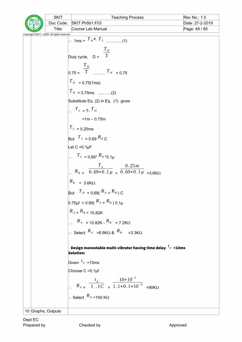
Design monostable multi-vibrator having time delay t p =10msSolution:
Given t p =10ms
Choose C =0.1µf
.‧. RA =
t p
1 . 1C =
10∗10−3
1.1∗0.1∗10−6 =90KΩ
.‧. Select RA =100 KΩ
10 Graphs, Outputs Dept ECPrepared by Checked by Approved

SKIT Teaching Process Rev No.: 1.0Doc Code: SKIT.Ph5b1.F03 Date: 27-2-2019
Title: Course Lab Manual Page: 50 / 65Copyright ©2017. cAAS. All rights reserved.
V UT =
23
V CC , V LT = 1/3 V CC
Note: For symmetrical astable multi-vibrator V OH = V OL
Monostable multi-vibrator
11 Results & Analysis 1. Unsymmetrical Astable multivibrator was designed and verified with % dutycycle =……2 symmetrical Astable multivibrator was designed and verified 3. Operation of monostable multi-vibrator is verified.
12 Application Areas Astable multivibrator:1. Square wave oscillator.
Dept ECPrepared by Checked by Approved

SKIT Teaching Process Rev No.: 1.0Doc Code: SKIT.Ph5b1.F03 Date: 27-2-2019
Title: Course Lab Manual Page: 51 / 65Copyright ©2017. cAAS. All rights reserved.
2 Free running ramp generator. Manostable multivibrator:1. Frequency divider.
2. Pulse stretcher.
13 Remarks
14 Faculty Signaturewith Date
Experiment 09 : RC PHASE SHIFT OSCILLATOR AND HARTLEY OSCILLATOR
- Experiment No.: 9 Marks 10 DatePlanned
DateConducted
1 Title RC Phase shift oscillator and Hartley oscillator2 Course Outcomes Simulate and analyze analog circuits that uses transistor and ICs for different
electronic applications.3 Aim To design and test the following tuned oscillator circuits for the given frequency. (a)
RC Phase Shift Oscillator using BJT. (b) Hartley Oscillator using BJT.4 Material /
EquipmentRequired
Dept ECPrepared by Checked by Approved

SKIT Teaching Process Rev No.: 1.0Doc Code: SKIT.Ph5b1.F03 Date: 27-2-2019
Title: Course Lab Manual Page: 52 / 65Copyright ©2017. cAAS. All rights reserved.
Hartley Oscillator using BJT.
5 Theory, Formula,Principle, Concept
RC PHASE SHIFT: An oscillator is an electronic circuit for generating an AC signal voltage with a DCsupply as theOnly input requirement. The frequency of the generated signal is decided by thecircuit elements used. An oscillator requires an amplifier, a frequency selectivenetwork and a positive feedback from the output to the input. The Barkhausencriterion for sustained oscillation is Aβ = 1 where A is the gain ofthe amplifier and βis the feedback factor (gain).The unity gain means signal is in phase. ( If the signalis1800 out of phase and gain will be -1). RC-Phase shift Oscillator has a CEamplifier followed by three sections of RC phase shift feed-back Networks. Theoutput of the last stage is return to the input of the amplifier. The values of R and Care chosen such that the phase shift of each RC section is 60º.Thus The RC laddernetwork produces a total phase shift of 180º between its input and output voltagefor the given frequency. Since CE Amplifier produces 180º phases shift. The totalphase shift from the base of the transistor around the circuit and back to the basewill be exactly 360º or 0º. This satisfies the Barkhausen condition for sustainingoscillations and total loop gain of this circuit is greater than or equal to 1, thiscondition used to generate the sinusoidal oscillations
HARTLEY: An oscillator is an electronic circuit for generating an AC signal voltage with a DCsupply as theOnly input requirement. The frequency of the generated signal is decided by thecircuit elements used. An oscillator requires an amplifier, a frequency selectivenetwork and a positive feedback from the output to the input. The Barkhausencriterion for sustained oscillation is Aβ = 1 where A is the gain ofthe amplifier and βis the feedback factor (gain).The unity gain means signal is in phase The Hartleyoscillator is an electronic oscillator circuit in which the oscillation frequency isdetermined by a tuned circuit consisting of capacitors and inductors, that is, an LCoscillator. The Hartley oscillator is distinguished by a tank circuit consisting of twoseries-connected coils (or, often, a tapped coil) in parallel with a capacitor, with anamplifier between the relatively high impedance across the entire LC tank and the
Dept ECPrepared by Checked by Approved

SKIT Teaching Process Rev No.: 1.0Doc Code: SKIT.Ph5b1.F03 Date: 27-2-2019
Title: Course Lab Manual Page: 53 / 65Copyright ©2017. cAAS. All rights reserved.
relatively low voltage/high current point between the coils. The Hartley oscillator isthe dual of the Colpitts oscillator which uses a voltage divider made of twocapacitors rather than two inductors. Although there is no requirement for there tobe mutual coupling between the two coil segments, the circuit is usuallyimplemented using a tapped coil, with the feedback taken from the tap, as shownhere. The optimal tapping point (or ratio of coil inductances) depends on theamplifying device used, which may be a bipolar junction transistor.
6 Procedure,Program, Activity,Algorithm, PseudoCode
1. Rig up the circuit as shown in figure 2. place all the required components from multi-sim library 3. click on run button and observe the out put To plot frequency response
1. Place the components in Multisim.
2. Rig up the circuit as shown in circuit diagram.
3. Click on the run button and Double click on Oscilloscope.
4. Observe the output waveforms on Oscilloscope.
5. Measure frequency of the output signal, compare it with theoretical
frequency.
HARTLEY:
6. To plot frequency response 7. Place the components in Multisim.
8. Rig up the circuit as shown in circuit diagram.
9. Click on the run button and Double click on Oscilloscope.
10. Observe the output waveforms on Oscilloscope.
11. Measure frequency of the output signal, compare it with theoretical
frequency.
Dept ECPrepared by Checked by Approved
SKIT Teaching Process Rev No.: 1.0Doc Code: SKIT.Ph5b1.F03 Date: 27-2-2019
Title: Course Lab Manual Page: 54 / 65Copyright ©2017. cAAS. All rights reserved.
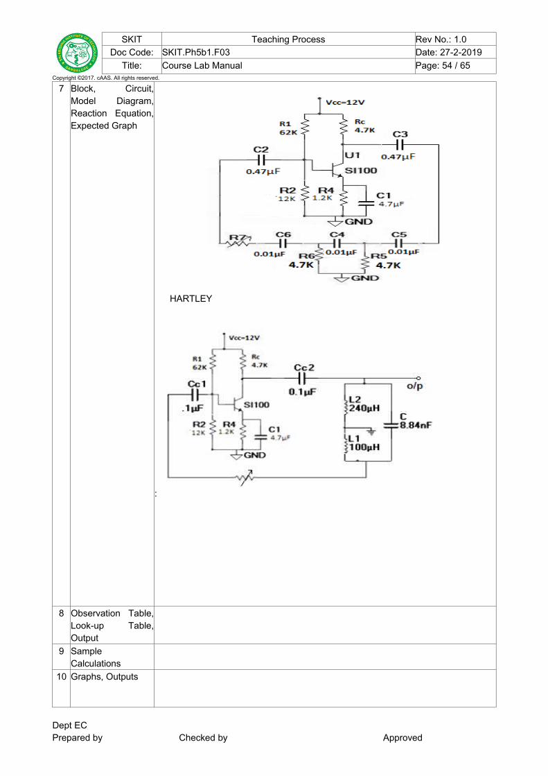
7 Block, Circuit,Model Diagram,Reaction Equation,Expected Graph
HARTLEY
:
8 Observation Table,Look-up Table,Output
9 SampleCalculations
10 Graphs, Outputs
Dept ECPrepared by Checked by Approved

SKIT Teaching Process Rev No.: 1.0Doc Code: SKIT.Ph5b1.F03 Date: 27-2-2019
Title: Course Lab Manual Page: 55 / 65Copyright ©2017. cAAS. All rights reserved.
11 Results & Analysis The RC Phase Shift Oscillator and Hartley simulated and output is verified
12 Application Areas RC phase shift oscillator is used in musical instrument, GPS unit and in voicesynthesis Hartley oscillator are used in radio receivers
13 Remarks14 Faculty Signature
with Date
Experiment 10 : NARROW BAND-PASS FILTER AND NARROW BAND-REJECT FILTER
- Experiment No.: 10 Marks 10 DatePlanned
DateConducted
1 Title Narrow Band-pass Filter and Narrow band-reject filter2 Course Outcomes Simulate and analyze analog circuits that uses transistor and ICs for different
electronic applications.
3 Aim To simulate and analyze the Narrow Band-pass Filter and Narrow band-rejectfilter
4 Material /EquipmentRequired
5 Theory, Formula,Principle, Concept
A narrow bandpass filter employing multiple feedback is depicted in figure. Thisfilter employs only one op-amp, as shown in the figure. In comparison to all thefilters discussed so far, this filter has some unique features that are given below.
1. It has two feedback paths, and this is the reason that it is called a multiple-feedback filter.
2. The op-amp is used in the inverting mode.
Dept ECPrepared by Checked by Approved
Vo
Vm
Wt
-Vm

SKIT Teaching Process Rev No.: 1.0Doc Code: SKIT.Ph5b1.F03 Date: 27-2-2019
Title: Course Lab Manual Page: 56 / 65Copyright ©2017. cAAS. All rights reserved.
The frequency response of a narrow bandpass filter is shown in fig(b).
Generally, the narrow bandpass filter is designed for specific values of centrefrequency fc and Q or fc and BW. The circuit components are determined from thefollowing relationships. For simplification of design calculations each of C1 andC2 may be taken equal to C.
R1 = Q/2∏ fc CAf
R2 =Q/2∏ fc C(2Q2-Af)
and R3 = Q / ∏ fc C
where Af, is the gain at centre frequency and is given as
Af = R3 / 2R1
The gain Af however must satisfy the condition Af < 2 Q2.
The centre frequency fc of the multiple feedback filter can be changed to a newfrequency fc‘ without changing, the gain or bandwidth. This is achieved simply bychanging R2 to R’2 so that
R’2 = R2 [fc/f’c]2
BAND REJECT FILTER:
This is also called a notch filter. It is commonly used for attenuation of a single frequency such as 60 Hz power line frequency hum. The most widely used notch filter is the twin-T network illustrated in fig. (a). This is a passive filter composed of two T-shaped networks. One T-network is made up of two resistors and a capacitor, while the other is made of two capacitors and a resistor.One drawback of above notch filter (passive twin-T network) is that it has relatively low figure of merit Q. However, Q of the network can be increased significantly if it is used with the voltage follower, as illustrated in fig. (a). Here the output of the volt-age follower is supplied back to the junction of R/2 and 2 C. The frequency response of the active notch filter is shown in fig (b).
Dept ECPrepared by Checked by Approved

SKIT Teaching Process Rev No.: 1.0Doc Code: SKIT.Ph5b1.F03 Date: 27-2-2019
Title: Course Lab Manual Page: 57 / 65Copyright ©2017. cAAS. All rights reserved.
Notch filters are most commonly used in communications and biomedicalinstruments for eliminating the undesired frequencies.
A mathematical analysis of this circuit shows that it acts as a lead-lag circuit with aphase angle, shown in fig. (b). Again, there is a frequency f c at which the phaseshift is equal to 0°. In fig. (c), the voltage gain is equal to 1 at low and highfrequencies. In between, there is a frequency fc at which voltage gain drops to zero.Thus such a filter notches out, or blocks frequencies near fc. The frequency atwhich maximum attenuation occurs is called the notch-out frequency given by
fn = Fc = 2∏RC
Notice that two upper capacitors are C while the capacitor in the centre of thenetwork is 2 C. Similarly, the two lower resistors are R but the resistor in the centreof the network is 1/2 R. This relationship must always be maintained.
Let us consider the narrow band notch filter circuit. We know that the notch filter isused to eliminate single frequency. Thus let us consider the frequency to eliminatebe 120 Hz. The capacitor value C= 0.33 µF.
By using the centre frequency fC = 1/(2πRC)
R = 1/(2πfCC) = 1 / (2πx120 x 0.33 x 10-6) = 4 kΩ
Thus, in order design the notch filter to eliminate 120 Hz frequency we have to taketwo parallel resistors with 4 kΩ each and the two capacitors in parallel with 0.33 µFeach.
Dept ECPrepared by Checked by Approved
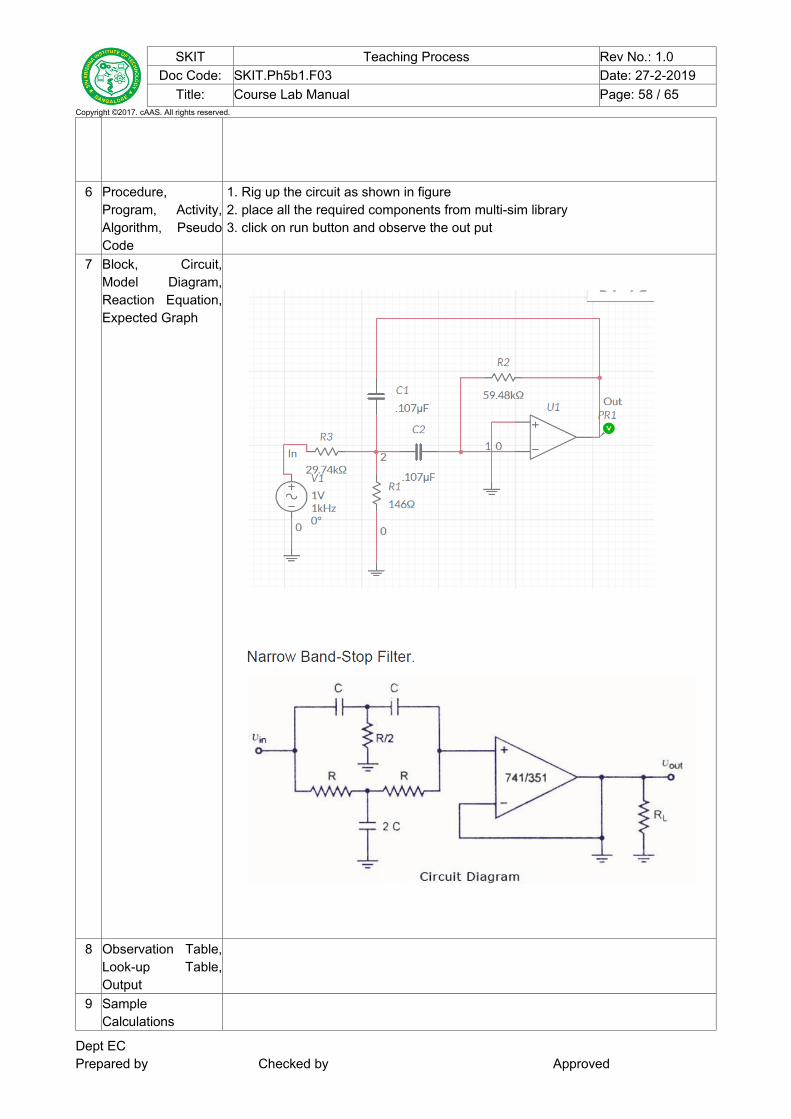
SKIT Teaching Process Rev No.: 1.0Doc Code: SKIT.Ph5b1.F03 Date: 27-2-2019
Title: Course Lab Manual Page: 58 / 65Copyright ©2017. cAAS. All rights reserved.
6 Procedure,Program, Activity,Algorithm, PseudoCode
1. Rig up the circuit as shown in figure 2. place all the required components from multi-sim library 3. click on run button and observe the out put
7 Block, Circuit,Model Diagram,Reaction Equation,Expected Graph
8 Observation Table,Look-up Table,Output
9 SampleCalculations
Dept ECPrepared by Checked by Approved

SKIT Teaching Process Rev No.: 1.0Doc Code: SKIT.Ph5b1.F03 Date: 27-2-2019
Title: Course Lab Manual Page: 59 / 65Copyright ©2017. cAAS. All rights reserved.
10 Graphs, Outputs
11 Results & Analysis The band-pass and band-reject filters are simulated and output is verified12 Application Areas Narrow band-pass used in wireless transceiver
Band reject filter is used in speaker systems , telephone technology13 Remarks14 Faculty Signature
with Date
Experiment 11 :PRECISION HALF AND FULL WAVE RECTIFIER
- Experiment No.: 11 Marks 10 DatePlanned
DateConducted
1 Title Precision Half and full wave rectifier2 Course Outcomes Simulate and analyze analog circuits that uses transistor and ICs for different
electronic applications.3 Aim To simulate and analyze Precision Half and full wave rectifier4 Material /
EquipmentRequired
5 Theory, Formula, When forward biased voltage is less than 0.7V, then diode is not conducting. In
Dept ECPrepared by Checked by Approved

SKIT Teaching Process Rev No.: 1.0Doc Code: SKIT.Ph5b1.F03 Date: 27-2-2019
Title: Course Lab Manual Page: 60 / 65Copyright ©2017. cAAS. All rights reserved.
Principle, Concept case of normal power rectifier input applied is much larger than 0.7V. So diode isnot operated. Therefore Op-amp is used to help diode to conduct.The precision rectifiers are classified in two categories.1.Precision Half wave rectifier 2. Precision Full wave Rectifier
1. Precision Half wave rectifier (HWR) :
In HWR, the diode conducts in one of the half cycles of applied ac input signal.Because of this we can classify HWR as positive PHWR (output is positive) andnegative PHWR (output is negative).In positive half cycle of applied ac input signal output of op-amp is negative, sodiode D1 is forward biased and D2 is reversed biased. The output of op-amp isvirtually shorted to ground and output voltage is zero.In negative half cycle of applied ac input signal output of op-amp is positive, sodiode D2 is forward biased and D1 is reversed biased. Non-saturated types of precision half wave rectifiers are suitable for high frequencyapplications. In HWR, the diode conducts in one of the half cycles of applied acinput signal. Design: In positive half cycle of applied ac input signal output of op-amp isnegative, so diode D1 is forward biased and D2 is reversed biased. The output ofop-amp is virtually shorted to ground and prevented going into saturation. Thusoutput voltage is zero.
∴Vo=0 V
In negative half cycle of applied ac input signal output of op-amp is positive, sodiode D2 is forward biased and D1 is reversed biased. The circuit now works as aninverting amplifier with gain of(-Rf/R1)Vo=Vin×ABut in negative half cycle input magnitude is negative therefore we get, Vo=(-V_in)[-Rf/R1]∴Vo=Rf/R1(Vin)Thus in negative half cycle output is positive with a gain of(Rf/R1 ).
2.Precision Full wave Rectifier: In PFWR, for both the half cycles output is produced & in one direction only. In positive half cycle of applied ac input signal, output of first op-amp (A1) is Negative. Therefore diode D2 is forward biased & diode D1 is reverse biased.
6 Procedure,Program, Activity,Algorithm, PseudoCode
7 Block, Circuit,Model Diagram,Reaction Equation,Expected Graph
Half-wave:
Dept ECPrepared by Checked by Approved

SKIT Teaching Process Rev No.: 1.0Doc Code: SKIT.Ph5b1.F03 Date: 27-2-2019
Title: Course Lab Manual Page: 61 / 65Copyright ©2017. cAAS. All rights reserved.
full wave:
8 Observation Table,Look-up Table,Output
9 SampleCalculations
10 Graphs, Outputs Half wave :
Dept ECPrepared by Checked by Approved
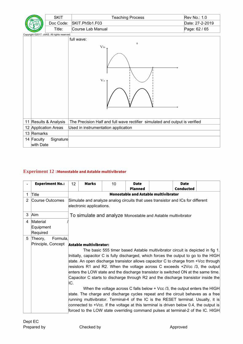
SKIT Teaching Process Rev No.: 1.0Doc Code: SKIT.Ph5b1.F03 Date: 27-2-2019
Title: Course Lab Manual Page: 62 / 65Copyright ©2017. cAAS. All rights reserved.
full wave:
11 Results & Analysis The Precision Half and full wave rectifier simulated and output is verified12 Application Areas Used in instrumentation application13 Remarks14 Faculty Signature
with Date
Experiment 12 :Monostable and Astable multivibrator
- Experiment No.: 12 Marks 10 DatePlanned
DateConducted
1 Title Monostable and Astable multivibrator2 Course Outcomes Simulate and analyze analog circuits that uses transistor and ICs for different
electronic applications.
3 Aim To simulate and analyze Monostable and Astable multivibrator4 Material /
EquipmentRequired
5 Theory, Formula,Principle, Concept
Astable multivibrator:
The basic 555 timer based Astable multivibrator circuit is depicted in fig 1.Initially, capacitor C is fully discharged, which forces the output to go to the HIGHstate. An open discharge transistor allows capacitor C to charge from +Vcc throughresistors R1 and R2. When the voltage across C exceeds +2Vcc /3, the outputenters the LOW state and the discharge transistor is switched ON at the same time.Capacitor C starts to discharge through R2 and the discharge transistor inside theIC.
When the voltage across C falls below + Vcc /3, the output enters the HIGHstate. The charge and discharge cycles repeat and the circuit behaves as a freerunning multivibrator. Terminal-4 of the IC is the RESET terminal. Usually, it isconnected to +Vcc. If the voltage at this terminal is driven below 0.4, the output isforced to the LOW state overriding command pulses at terminal-2 of the IC. HIGH
Dept ECPrepared by Checked by Approved

SKIT Teaching Process Rev No.: 1.0Doc Code: SKIT.Ph5b1.F03 Date: 27-2-2019
Title: Course Lab Manual Page: 63 / 65Copyright ©2017. cAAS. All rights reserved.
state and LOW state time periods are governed by the charge (+ Vcc /3 to +2Vcc /3) and discharge (+2Vcc /3 to +Vcc /3) timings. These are given by (1) and (2)respectively.HIGH state time period, THIGH= 0.69 x (R1+R2) x C LOW state time period, TLOW= 0.69 x R2 x C
6 Procedure,
Program, Activity,Algorithm, PseudoCode
1. Rig up the circuit as shown in figure 2. place all the required components from multi-sim library 3. click on run button and observe the out put
7 Block, Circuit,Model Diagram,Reaction Equation,Expected Graph
Astable multivibrator:
monostable multi-vibrator:
8 Observation Table,Dept ECPrepared by Checked by Approved

SKIT Teaching Process Rev No.: 1.0Doc Code: SKIT.Ph5b1.F03 Date: 27-2-2019
Title: Course Lab Manual Page: 64 / 65Copyright ©2017. cAAS. All rights reserved.
Look-up Table,Output
9 SampleCalculations
10 Graphs, Outputs Astable multi-vibrator
monostable multi-vibrator
11 Results & Analysis The Astable and manostable multi-vibrator is simulated and output is verified12 Application Areas Astable multivibrator:
2. Square wave oscillator.
2 Free running ramp generator.
Dept ECPrepared by Checked by Approved
SKIT Teaching Process Rev No.: 1.0Doc Code: SKIT.Ph5b1.F03 Date: 27-2-2019
Title: Course Lab Manual Page: 65 / 65Copyright ©2017. cAAS. All rights reserved.
Manostable multivibrator:2. Frequency divider.
2. Pulse stretcher.
13 Remarks14 Faculty Signature
with Date
Dept ECPrepared by Checked by Approved