converter for audio applications using an fpga650302/fulltext01.pdf · implementation of a low-cost...
TRANSCRIPT

Institutionen för systemteknikDepartment of Electrical Engineering
Examensarbete
Implementation of a Low-Cost Analog-to-DigitalConverter for Audio Applications Using an FPGA
Examensarbete utfört i Elektroniksystemvid Tekniska högskolan vid Linköpings universitet
av
Johan Hellman
LiTH-ISY-EX--13/4711--SE
Linköping 2013
Department of Electrical Engineering Linköpings tekniska högskolaLinköpings universitet Linköpings universitetSE-581 83 Linköping, Sweden 581 83 Linköping

Implementation of a Low-Cost Analog-to-DigitalConverter for Audio Applications Using an FPGA
Examensarbete utfört i Elektroniksystemvid Tekniska högskolan vid Linköpings universitet
av
Johan Hellman
LiTH-ISY-EX--13/4711--SE
Handledare: Erik LindahlActiwave AB
Examinator: Kent Palmkvistisy, Linköpings universitet
Linköping, 9 september 2013

Avdelning, InstitutionDivision, Department
ElektroniksystemDepartment of Electrical EngineeringSE-581 83 Linköping
DatumDate
2013-09-09
SpråkLanguage
Svenska/Swedish
Engelska/English
RapporttypReport category
Licentiatavhandling
Examensarbete
C-uppsats
D-uppsats
Övrig rapport
URL för elektronisk version
http://urn.kb.se/resolve?urn=urn:nbn:se:liu:diva-96009
ISBN
—
ISRN
LiTH-ISY-EX--13/4711--SE
Serietitel och serienummerTitle of series, numbering
ISSN
—
TitelTitle
Implementering av en analog till digital omvandlare med låg kostnad för ljudapplikationermed hjälp av en FPGA
Implementation of a Low-Cost Analog-to-Digital Converter for Audio Applications Using anFPGA
FörfattareAuthor
Johan Hellman
SammanfattningAbstract
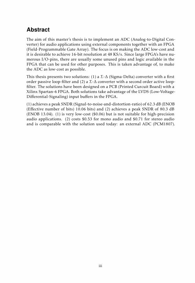
The aim of this master’s thesis is to implement an ADC (Analog-to-Digital Converter) foraudio applications using external components together with an FPGA (Field-ProgrammableGate Array). The focus is on making the ADC low-cost and it is desirable to achieve 16-bitresolution at 48 KS/s. Since large FPGA’s have numerous I/O-pins, there are usually someunused pins and logic available in the FPGA that can be used for other purposes. This istaken advantage of, to make the ADC as low-cost as possible.
This thesis presents two solutions: (1) a Σ-∆ (Sigma-Delta) converter with a first order pas-sive loop-filter and (2) a Σ-∆ converter with a second order active loop-filter. The solutionshave been designed on a PCB (Printed Curcuit Board) with a Xilinx Spartan-6 FPGA. Bothsolutions take advantage of the LVDS (Low-Voltage-Differential-Signaling) input buffers inthe FPGA.
(1) achieves a peak SNDR (Signal-to-noise-and-distortion-ratio) of 62.3 dB (ENOB (Effectivenumber of bits) 10.06 bits) and (2) achieves a peak SNDR of 80.3 dB (ENOB 13.04). (1) isvery low-cost ($0.06) but is not suitable for high-precision audio applications. (2) costs $0.53for mono audio and $0.71 for stereo audio and is comparable with the solution used today:an external ADC (PCM1807).
NyckelordKeywords ADC, Sigma-Delta, FPGA, LVDS

Abstract
The aim of this master’s thesis is to implement an ADC (Analog-to-Digital Con-verter) for audio applications using external components together with an FPGA(Field-Programmable Gate Array). The focus is on making the ADC low-cost andit is desirable to achieve 16-bit resolution at 48 KS/s. Since large FPGA’s have nu-merous I/O-pins, there are usually some unused pins and logic available in theFPGA that can be used for other purposes. This is taken advantage of, to makethe ADC as low-cost as possible.
This thesis presents two solutions: (1) a Σ-∆ (Sigma-Delta) converter with a firstorder passive loop-filter and (2) a Σ-∆ converter with a second order active loop-filter. The solutions have been designed on a PCB (Printed Curcuit Board) with aXilinx Spartan-6 FPGA. Both solutions take advantage of the LVDS (Low-Voltage-Differential-Signaling) input buffers in the FPGA.
(1) achieves a peak SNDR (Signal-to-noise-and-distortion-ratio) of 62.3 dB (ENOB(Effective number of bits) 10.06 bits) and (2) achieves a peak SNDR of 80.3 dB(ENOB 13.04). (1) is very low-cost ($0.06) but is not suitable for high-precisionaudio applications. (2) costs $0.53 for mono audio and $0.71 for stereo audioand is comparable with the solution used today: an external ADC (PCM1807).
iii

Acknowledgments
First, I wish to thank Tina Kallio for her support during the thesis work. She hasgiven me guidance and perspective in stressful moments.
I would also like to thank Dr. J Jacob Wikner for the help with Σ-∆ convertersand Op-amps, and Dai Zhang, who helped me with FFT and providing me a FFTscript.
Thanks to my examiner Kent Palmkvist for making this thesis possible.
At last (but not least), I would like to express my gratitude to Actiwave AB for thisthesis and letting me do the work at their office in Stockholm. Especially thanksto my supervisor at Actiwave AB, Erik Lindahl, for all his help and support.
Stockholm, September 2013Johan Hellman
v


Contents
Notation ix
1 Introduction 11.1 Problem formulation . . . . . . . . . . . . . . . . . . . . . . . . . . 11.2 Related work . . . . . . . . . . . . . . . . . . . . . . . . . . . . . . . 21.3 Thesis outline . . . . . . . . . . . . . . . . . . . . . . . . . . . . . . 2
2 System Overview 52.1 The Complete System . . . . . . . . . . . . . . . . . . . . . . . . . . 52.2 The Xilinx Spartan-6 FPGA . . . . . . . . . . . . . . . . . . . . . . 6
2.2.1 LVDS . . . . . . . . . . . . . . . . . . . . . . . . . . . . . . . 62.3 The Analog Audio Input Signal . . . . . . . . . . . . . . . . . . . . 72.4 Analog to Digital Converters Suited for Audio Applications . . . . 8
3 Theory 93.1 Analog to Digital Conversion . . . . . . . . . . . . . . . . . . . . . 9
3.1.1 Sampling . . . . . . . . . . . . . . . . . . . . . . . . . . . . . 103.1.2 Quantization . . . . . . . . . . . . . . . . . . . . . . . . . . . 113.1.3 Performance Metrics . . . . . . . . . . . . . . . . . . . . . . 11
3.2 Understanding Σ-∆ ADC . . . . . . . . . . . . . . . . . . . . . . . . 133.2.1 An Oversampling ADC . . . . . . . . . . . . . . . . . . . . . 133.2.2 Noise Shaping . . . . . . . . . . . . . . . . . . . . . . . . . . 153.2.3 Higher Order Σ-∆ Modulators . . . . . . . . . . . . . . . . . 173.2.4 Continuous-time Σ-∆ ADC . . . . . . . . . . . . . . . . . . 183.2.5 Inherent Anti-Aliasing Filter in CT Σ-∆ ADC . . . . . . . . 21
3.3 Non-idealities in CT Σ-∆ Modulator . . . . . . . . . . . . . . . . . 223.3.1 Circuit Noise . . . . . . . . . . . . . . . . . . . . . . . . . . . 223.3.2 Excess Loop Delay . . . . . . . . . . . . . . . . . . . . . . . 233.3.3 Clock Jitter . . . . . . . . . . . . . . . . . . . . . . . . . . . . 233.3.4 Unequal Rise/Fall Time of DAC . . . . . . . . . . . . . . . . 243.3.5 Operational Amplifier Non-Idealities . . . . . . . . . . . . . 24
3.4 Digital Filtering and Decimation . . . . . . . . . . . . . . . . . . . 263.4.1 CIC filters . . . . . . . . . . . . . . . . . . . . . . . . . . . . 27
vii

viii CONTENTS
4 Test Setup 294.1 Test Setup . . . . . . . . . . . . . . . . . . . . . . . . . . . . . . . . 294.2 Control of Test Setup Quality . . . . . . . . . . . . . . . . . . . . . 30
5 Implementation of a Passive Σ-∆ Converter 335.1 System Overview . . . . . . . . . . . . . . . . . . . . . . . . . . . . 335.2 The Passive Σ-∆ Modulator . . . . . . . . . . . . . . . . . . . . . . . 34
5.2.1 Realization of the Passive Σ-∆ Converter . . . . . . . . . . . 365.2.2 Simulation Results . . . . . . . . . . . . . . . . . . . . . . . 375.2.3 Non-idealities in the Passive Σ-∆ modulator . . . . . . . . . 38
5.3 The CIC filter . . . . . . . . . . . . . . . . . . . . . . . . . . . . . . 395.4 The FIR filter . . . . . . . . . . . . . . . . . . . . . . . . . . . . . . . 405.5 Results . . . . . . . . . . . . . . . . . . . . . . . . . . . . . . . . . . 41
5.5.1 FPGA resources . . . . . . . . . . . . . . . . . . . . . . . . . 435.6 Discussion . . . . . . . . . . . . . . . . . . . . . . . . . . . . . . . . 43
6 Implementation of a Second Order Σ-∆ Converter 456.1 System Overview . . . . . . . . . . . . . . . . . . . . . . . . . . . . 456.2 The 2nd Order CT Σ-∆ Modulator . . . . . . . . . . . . . . . . . . . 46
6.2.1 Realization of the 2nd order CT Σ-∆ modulator . . . . . . . 486.2.2 Simulation Results . . . . . . . . . . . . . . . . . . . . . . . 506.2.3 Non-idealities in the ∆-Σ modulator . . . . . . . . . . . . . 51
6.3 CIC filter . . . . . . . . . . . . . . . . . . . . . . . . . . . . . . . . . 526.4 FIR filter . . . . . . . . . . . . . . . . . . . . . . . . . . . . . . . . . 536.5 Results . . . . . . . . . . . . . . . . . . . . . . . . . . . . . . . . . . 53
6.5.1 FPGA resources . . . . . . . . . . . . . . . . . . . . . . . . . 556.6 Discussion . . . . . . . . . . . . . . . . . . . . . . . . . . . . . . . . 56
7 Conclusions and Future Work 577.1 Conclusions . . . . . . . . . . . . . . . . . . . . . . . . . . . . . . . 577.2 Future Work . . . . . . . . . . . . . . . . . . . . . . . . . . . . . . . 59
List of Figures 61
List of Tables 64
Bibliography 65
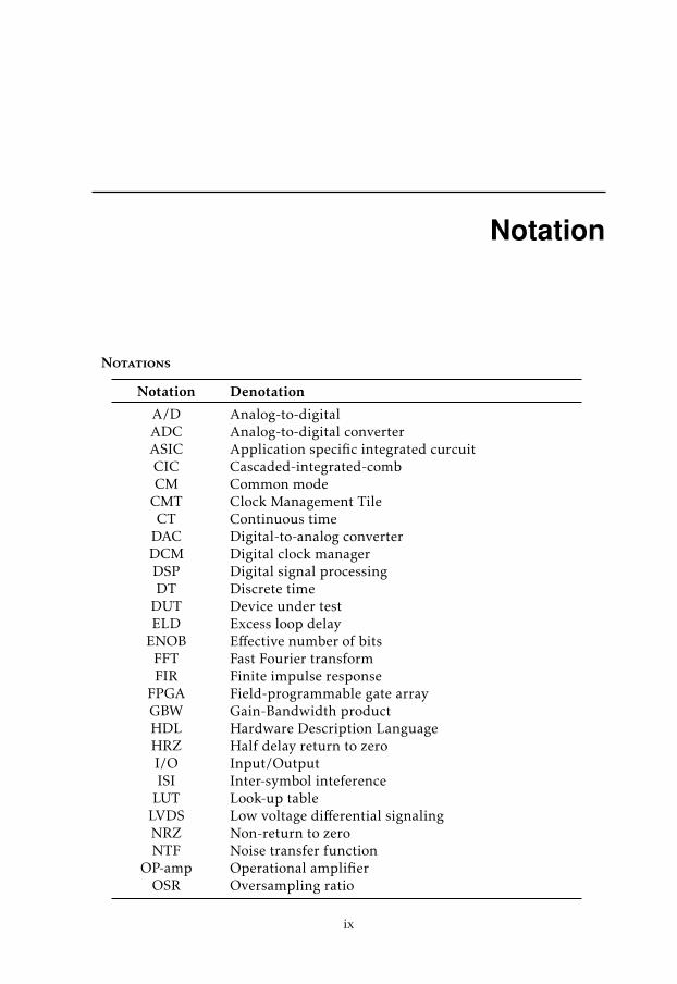
Notation
Notations
Notation Denotation
A/D Analog-to-digitalADC Analog-to-digital converterASIC Application specific integrated curcuitCIC Cascaded-integrated-combCM Common mode
CMT Clock Management TileCT Continuous time
DAC Digital-to-analog converterDCM Digital clock managerDSP Digital signal processingDT Discrete time
DUT Device under testELD Excess loop delay
ENOB Effective number of bitsFFT Fast Fourier transformFIR Finite impulse response
FPGA Field-programmable gate arrayGBW Gain-Bandwidth productHDL Hardware Description LanguageHRZ Half delay return to zeroI/O Input/OutputISI Inter-symbol inteference
LUT Look-up tableLVDS Low voltage differential signalingNRZ Non-return to zeroNTF Noise transfer function
OP-amp Operational amplifierOSR Oversampling ratio
ix

x Notation
Notations
Notation Denotation
PC Personal computerPCB Printed curcuit boardPLL Phase-locked loopsPSD Power spectrum densityRAM Random access memoryRMS Root-mean-squaredRZ Return to zeroS/s Samples per secondΣ-∆ Sigma-DeltaSCR Switched capacitor resistor
SFDR Spurious-free dynamic rangeSNDR Signal-to-noise and distortion ratioSNR Signal-to-noise ratio
S/PDIF Sony/Philips Digital Interconnect FormatSR Slew rate
STF Signal transfer functionSQNR Signal-to-quantization-noise ratioTHD Total harmonic distortion

1Introduction
FPGA (Field-Programmable Gate Array) based solutions in consumer electron-ics have gained popularity due to low cost and high performance. The time-to-market is also shorter and the financial risk is lower compared to ASIC (Appli-cation Specific Integrated Circuit). One component that is missing in a low-costFPGA is the ability to convert an analog signal to its digital counterpart.
An FPGA is an integrated curcuit, which have a large number of logic resourcesthat can be configured to implement complex digital algorithms. The configura-tion can be done after manufacturing and is specified using a HDL (Hardware de-scription language). This thesis will take advantage of the strength of the FPGA.
The aim of this thesis is to implement an ADC (Analog-to-Digital Converter)for audio applications using an FPGA together with external components. Seefigure 2.1 for an illustration of the complete system. Two solutions are presented:(1) a Σ-∆ converter with a first order passive loop-filter and (2) a Σ-∆ conveterwith a second order active loop-filter. In both solutions, the FPGA will mainly beused to implement digital filters.
1.1 Problem formulation
This master thesis is done at Actiwave AB, a Swedish company which uses algo-rithms to make better sound quality in loudspeakers. The aim is to implementan ADC for audio applications using external components and an FPGA as illus-trated in figure 2.1. Today, Actiwave AB uses an external ADC for conversionemploying a 24-bit 99 dB SNR (93 dB SNDR) audio ADC (PCM1807) from TexasInstruments [21]. The main objective is to try eliminate the external ADC andreplace it with external components and use the power of the FPGA. The goal is
1

2 1 Introduction
therefore to make it low-cost and it is desirable to achieve CD quality, i.e. 16-bitresolution at 44.1 KS/s. In this thesis I will use 48 KS/s and the goal is to achieve16-bit resolution. The term "low-cost", in this thesis, is only focusing on the exter-nal components. The goal is to keep the total cost of the external components at aminimum. However, the FPGA resources used should also be kept at a minimum.
Since large FPGA’s have numerous I/O-pins, there are usually some unused pinsand logic available in the FPGA that can be used for other purposes. This is takenadvantage of, to make the ADC as low-cost as possible.
1.2 Related work
Analog to digital conversion is not a new topic; it has been along since the verystart of mixed signal electronics. There have been several related work regardingADC and FPGA’s, e.g. Lattice [13] uses the LVDS buffer on the FPGA togetherwith an RC-network to implement a simple Σ-∆ ADC. In 2004, Fabio Sousa etal. [19] presented a paper that also describes the implementation of Sigma-Deltathat takes the advantage of the LVDS input buffers. In 2011, Axel Zimmermanet al. [27] presented a combined solution for ADC and DAC using an FPGA. TheADC is also employing the LVDS input buffer as a comparator.
However, none of the above presented papers have a focus on low-cost and theyhave not used any active components outside the FPGA.
1.3 Thesis outline
The outline of this master thesis is as follows:
• Chapter 2 describes a system overview, the Xilinx Spartan-6 FPGA andwhat type of ADC architecture that is suited for audio applications.
• In Chapter 3 the theory of analog to digital conversion is described and inparticular the Σ-∆ ADC along with digital filtering.
• Chapter 5 describes the implementation of a first order Σ-∆ ADC usingonly passive components as a loop-filter.
• In Chapter 6 the implementation of the second order Σ-∆ ADC using anactive filter as loop-filter is described.
• Chapter 7 presents the conclusions and what can be done in the future.
See Table 1.1 for an illustration of the outline of the thesis.

1.3 Thesis outline 3
Introduction(Chapter 1)
↓System Overview
(Chapter 2)↓
Theory(Chapter 3)
↓Test Setup(Chapter 4)
↓↓ ↓
Impl. of a Passive Impl. of a SecondΣ-∆ Converter order Σ-∆ Converter
(Chapter 5) (Chapter 6)↓ ↓
System SystemOverview Overview
(Section 5.1) (Section 6.1)↓ ↓
The Modulator The Modulator(Section 5.2) (Section 6.2)
↓ ↓CIC filter CIC filter
(Section 5.3) (Section 6.3)↓ ↓
FIR filter FIR filter(Section 5.4) (Section 6.4)
↓ ↓Results Results
(Section 5.5) (Section 6.5)↓ ↓
Discussion Discussion(Section 5.6) (Section 6.6)
↓ ↓↓
Conclusion andFuture Work(Chapter 7)
Table 1.1: The outline of the thesis.


2System Overview
In this chapter, there will be a descirbed overview of the system along with thebuilding blocks, such as the FPGA and LVDS input buffer. A discussion about thekind of ADC architecture that is suited for audio applications is also presented.
2.1 The Complete System
The ADC is implemented on a PCB (Printed Curcuit Board) containing a XilinxXC6SLX9 (Spartan-6) FPGA in a TQG144 package and external components. SeeFigure 2.1 for the overview of the system. The external components could beanything, but in this thesis there will be a focus on low-cost. Therefore the totalcost of the external components should be kept at a minimum.
XilinxXC6SLX9FPGATQG144
ExternalComponents
AnalogIn Digital
Out
PCB
Figure 2.1: The complete system.
5
6 2 System Overview
2.2 The Xilinx Spartan-6 FPGA
The FPGA contains resources according to Table 2.1 [25]. Each DSP48A1 slicecontains an 18 × 18 bits multiplier, and adder and an accumulator. Every CMT(Clock Management Tile) is containing two DCMs (Digital Clock Managers) andone PLL (Phase-Locked Loops). The FPGA is using 3.3V single supply.
Block Resource AmountLogic Cells 9152
Configurable Slices 1430Logic Blocks Flip-Flops 11440
(CLBs) Max Distributed RAM (Kb) 90Block RAM 18 Kb 32
Other DSP48A1 Slices 16CMTs 2
Total I/O Banks 4User I/O 102
Table 2.1: Xilinx Spartan-6 XC6LX9 FPGA Features (TQG144 package).
2.2.1 LVDS
The Spartan-6 FPGA is supporting the LVDS (Low Voltage Differential Signal-ing) standard. LVDS is a serial data communication channel transmitted over adifferential pair allowing high speed and low power compared to single endedcommunication [18]. Figure 2.2 shows a simplified schematic of the LVDS driverand reciever. The driver sends a 3.5mA current through the 100Ω resistor, re-sulting in a 350mV swing. By changing the direction of the current results in aopposite polarity at the reciever [20]. The LVDS reciever is basically a high-speedcomparator, allowing speed up to hundreds of megabits/s [18]. Since a lot of A/Dconverters are centered around one of several comparators, the LVDS buffer is agood component for this thesis.
100Ω
3.5mASender Reciever
+
-
+
-
Data in Data out
Figure 2.2: Simplified LVDS schematic [18].
Table 2.2 shows the LVDS input buffer specification of the Xilinx Spartan-6 [26].One thing should be noted, the LVDS input buffer specification in Table 2.2 onlyspecifies the LVDS input buffer so it complies with the LVDS standard. The LVDS

2.3 The Analog Audio Input Signal 7
input buffer itself could work with larger VID and VICM ranges within the supplyrange.
VIN Differential (VID) VIN Common Mode (VICM)Min [mV] Max [mV] Max [V] Min [V]
100 600 0.3 2.35
Table 2.2: LVDS I/O Standard Input Levels Xilinx Spartan-6.
Some comparators have hysteresis [1], which prevents the comparator to switchstates rapidly in a noisy environment. Figure 2.3 illustrates the transfer functionof a comparator with hysteresis. Because the LVDS buffer is essentially a com-parator, it may have hysteresis. According to [19], the hysteresis of the LVDSbuffer in an Altera FPGA have a hysteresis less than 30mV. I will assume that thehysteresis of the LVDS buffer in Xilinx FPGA have the same order of magnitude.
ΔVin
Vout
Hysteresis
VoutΔVin
Figure 2.3: Hysteresis of a comparator [1].
2.3 The Analog Audio Input Signal
The input signal has to be characterized, in order to design the ADC suited for theparticular input signal. The analog audio input signal, in this thesis, is assumedto have the specification according to Table 2.3.
Specification ValueAmplitude (max) 1.65V (3.3Vpp)
Bandwidth 20Hz –20KHz
Table 2.3: Analog audio input signal specification.
8 2 System Overview
Res
olut
ion-
[bits
]
Conversion-Rate-[Hz]
8
10
12
14
16
18
20
22
24
10 100 1K 10K 100K 1M 10M 100M 1G
Sigma5Delta
Sigm
a5Del
ta
SAR
Pipeline
IndustrialMeasurement
Voicef-Audio
Data-Acquisition
High-Speed
State-of-the-art-2005
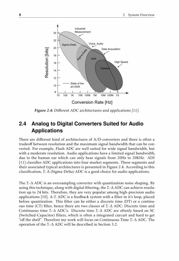
Figure 2.4: Different ADC architectures and applications [11].
2.4 Analog to Digital Converters Suited for AudioApplications
There are different kind of architectures of A/D-converters and there is often atradeoff between resolution and the maximum signal bandwidth that can be con-verted. For example, Flash ADC are well suited for wide signal bandwidth, butwith a moderate resolution. Audio applications have a limited signal bandwidth,due to the human ear which can only hear signals from 20Hz to 20KHz. ADI[11] classifies ADC applications into four market segments. These segments andtheir associated typical architectures is presented in Figure 2.4. According to thisclassification, Σ-∆ (Sigma-Delta) ADC is a good choice for audio applications.
The Σ-∆ ADC is an oversampling converter with quantization noise shaping. Byusing this technique, along with digital filtering, the Σ-∆ ADC can achieve resolu-tion up to 24 bits. Therefore, they are very popular among high-precision audioapplications [10]. ∆-Σ ADC is a feedback system with a filter in it’s loop, placedbefore quantization. This filter can be either a discrete time (DT) or a continu-ous time (CT) filter, hence there are two classes of Σ-∆ ADC: Discrete time andContinuous time Σ-∆ ADC’s. Discrete time Σ-∆ ADC are oftenly based on SC(Switched-Capacitor) filters, which is often a integrated curcuit and hard to get"off the shelf". Therefore my work will focus on Continuous Time Σ-∆ ADC. Theoperation of the Σ-∆ ADC will be described in Section 3.2.

3Theory
In this chapter the fundamental operation of an ADC is described. Furthermore,it describes the basic operation of a Σ-∆ converter and in particualar the CT Σ-∆converter. Since the Σ-∆ converter is a oversampling converter, there is a chapterabout digital filtering and decimation (downsampling).
3.1 Analog to Digital Conversion
The main objective of an ADC is to convert an analog signal into its digital coun-terpart, so it can be further processed by digital circuits. An analog signal is in itsnature continuous in both time and amplitude, while a digital signal is discretein both time and amplitude. This process can be divided into two sections: Sam-pling (described in Section 3.1.1) and Quantization (described in Section 3.1.2).See Figure 3.1 for an illustration of the ADC system.
ADC/Quantizer DSP
Ts
Analog in
x(t)
Sampling
x[n] y[n]
Figure 3.1: From analog input signal, x(t), to output, y[n], which is laterprocessed by e.g. a DSP [23].
9

10 3 Theory
3.1.1 Sampling
Sampling is a process that convert a continuous time signal into a discrete timesignal. The signal, x(t), is sampled at a uniformly spaced time intervals, Ts (seeFigure 3.2) [2]:
TS
x(t) x[n]
Figure 3.2: The sampling process.
x[n] = x(nTs) (3.1)
where x[n] is the sampled signal. This can be seen as multiplying the signal withdirac pulses at nTs [5]:
xp(t) = x(t)p(t) =∞∑
n=−∞x(nTs)δ(t − nTs) (3.2)
where
p(t) =∞∑
n=−∞δ(t − nTs) (3.3)
and
δ(t) =
1, t = 00, t , 1 (3.4)
The Fourier transform of the sampled function xp(t) is [5]:
Xp(ω) =1
2πX(ω) ∗ P (ω) =
1Ts
∞∑k=−∞
X(ω − kωs), (3.5)
ωs = 2πfs =2πTs.
One can see that the frequency components in x(t) is reapeated every multiple ofωs. To prevent aliasing and to fully reconstruct the signal, the Nyquist theoremhas to be fulfilled [5]:
fs > 2fB, (3.6)

3.1 Analog to Digital Conversion 11
where fB is the bandwidth of the analog input signal. An anti-aliasing filter isusually placed before the sampling [2], to prevent this from happening. This isshown in Figure 3.3.
FrequencyfB fS 3fS2fS
Anti aliasing filter
Image Image Image ImageInput
Figure 3.3: xp in the frequency domain [5].
The Nyquist theorem sets a boundary for the sampling frequency. A/D-convertesthat operates close to the boundary is called Nyquist-rate convertes and convert-ers that operate at a much higher frequency is called oversampling ADCs. Over-sampling ADCs are explained in Section 3.2.1.
3.1.2 Quantization
The analog signal must also be mapped to discrete levels. This is done by thequantization process. The wordlength, in number of bits N , decides the resolu-tion of the ADC and the number of leves is 2N . This is shown in Figure 3.4awith N = 3. The finite wordlength of the ADC results in a quantization error,∆, which is bound between − q2 < ∆ < + q
2 where q is one LSB. The ∆-function isillustrated in Figure 3.4b. This quantization error is assumed to be white noiseand uncorrelated with the input signal and is referred to as quantization noise.The total quantization noise power is (mean-squared) [5]:
e2q =
1q
+q/2∫−q/2
∆2 d∆ =q2
12, (3.7)
which is measured from DC to fs/2. The power spectral density (PSD) for thequantization noise is [5]:
Seq (f ) =e2q
fs/2. (3.8)
3.1.3 Performance Metrics
Performance metrics are used to characterize the ADC. The metrics can be di-vided in two categories: static and dynamic. Static metrics are analyzed in thetime domain, while dynamic metrics are analyzed in the frequency domain [5].In this thesis there will be focus on the dynamic metrics only. Below follows apresentation of the dynamic metrics used in this work.

12 3 Theory
−2 0 2 4 6 8 10−2
0
2
4
6
8
10
VIN
VO
UT
(a) No quantization (straight line) andquantized signal.
−2 0 2 4 6 8 10−2
−1
0
1
2
VIN
Err
or
(b) Error signal, Error = V outideal −V outquantized .
Figure 3.4: Illustration of quantization.
SNR
SNR (Signal-to-Noise-Ratio) is defined as the ratio between the signal power andthe noise power (excluding DC component) [5]:
SNR = 10log10
S2RMS
E2RMS
[dB] (3.9)
SQNR
SQNR (Signal-to-Quantization-Noise-Ratio) is, compared to SNR, only focusingon the noise generated by the quantizer (quantization noise) [5]:
SQNR = 10log10
S2RMS
E2Q,RMS
[dB] (3.10)
SNDR
SNDR (Signal-to-Noise-and-Distortion-Ratio) is, in contrast to SNR, also includ-ing the power of the distortion (excluding DC component) [5]:
SNDR = 10log10
S2RMS
E2RMS + E2
D
[dB] (3.11)
SNDR is sometimes referred to as SINAD or THD+N.
THD
THD (Total Harmonic Distortion) is defined as the ratio between the signal powerand the power of all the harmonic distiortion [5]:
T HD = 10log10
S2RMS
E2D
[dB] (3.12)

3.2 Understanding Σ-∆ ADC 13
ENOB
ENOB (Effective-Number-of-Bits) is a measure of how many bits are above thenoise floor. The ENOB formula is derived from the theoretical SNR of a N-bitADC (SNR = 6.02N + 1.76[dB]), where SNR and N is substituted by SNDR andENOB, respectively [5]:
ENOB =SNDR[dB] − 1.76
6.02[bits] (3.13)
SFDR
SFDR (Spurious-Free-Dynamic-Range) is a defined as the ratio between the sig-nal power and the power of the worst spurious signal [5]. This is illustrated inFigure 3.5, where dBFS stands for dB relative to the full-scale (FS) and dBc standsfor dB relative to the carrier (c).
0 0.05 0.1 0.15 0.2 0.25 0.3 0.35 0.4 0.45 0.5−100
−80
−60
−40
−20
0
Normalized Frequency f/fs [Hz]
PS
D [d
B]
40 dBFS
20 dBc
Figure 3.5: Illustration of SFDR.
3.2 Understanding Σ-∆ ADC
This section describes the basic operation of Σ-∆ converters.
3.2.1 An Oversampling ADC
Σ-∆ ADC is an oversampled A/D-converter which converts the signal in a muchhigher sampling frequency. The oversampling ratio (OSR) defined as [10]:
OSR =fs
2fB. (3.14)
14 3 Theory
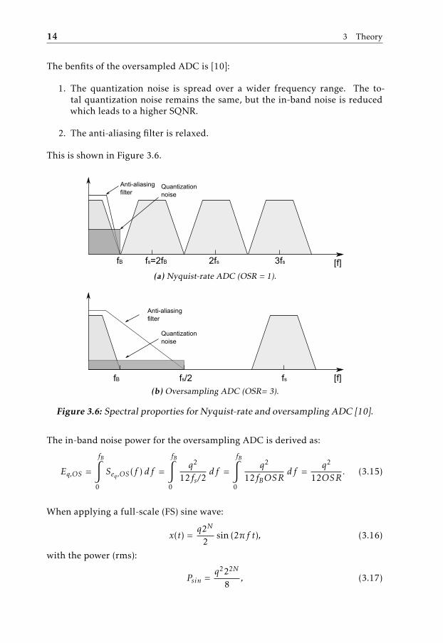
The benfits of the oversampled ADC is [10]:
1. The quantization noise is spread over a wider frequency range. The to-tal quantization noise remains the same, but the in-band noise is reducedwhich leads to a higher SQNR.
2. The anti-aliasing filter is relaxed.
This is shown in Figure 3.6.
fB fs=2fB [f]
Anti-aliasingfilter
Quantizationnoise
2fs 3fs
(a) Nyquist-rate ADC (OSR = 1).
fB fs/2 fs [f]
Anti-aliasingfilter
Quantizationnoise
(b) Oversampling ADC (OSR= 3).
Figure 3.6: Spectral proporties for Nyquist-rate and oversampling ADC [10].
The in-band noise power for the oversampling ADC is derived as:
Eq,OS =
fB∫0
Seq ,OS (f ) df =
fB∫0
q2
12fs/2df =
fB∫0
q2
12fBOSRdf =
q2
12OSR. (3.15)
When applying a full-scale (FS) sine wave:
x(t) =q2N
2sin (2πf t), (3.16)
with the power (rms):
Psin =q222N
8, (3.17)
3.2 Understanding Σ-∆ ADC 15
the maximum SQNR for the oversampling ADC becomes:
SQNROS = 10log10(PsinEq
) = 6.02N + 1.76 + 10log10(OSR). [dB] (3.18)
For a comparison, a Nyquist-rate ADC with an OSR = 1, the maximum SQNRbecomes:
SQNRNyquist = 6.02N + 1.76. [dB] (3.19)
The SQNR increases 3dB for every doubling of the OSR.
The oversampling ADC is usually followed by a digital low-pass filter which re-moves the out-of-band noise. The digital low-pass filter is followed by a decima-tor to get downsampled to the Nyquist-rate.
3.2.2 Noise Shaping
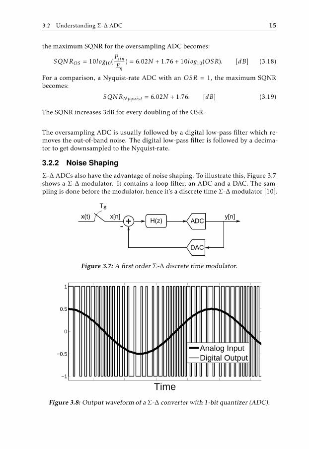
Σ-∆ ADCs also have the advantage of noise shaping. To illustrate this, Figure 3.7shows a Σ-∆ modulator. It contains a loop filter, an ADC and a DAC. The sam-pling is done before the modulator, hence it’s a discrete time Σ-∆ modulator [10].
+ H(z) ADC
DAC
Ts
x(t) x[n]
-y[n]
Figure 3.7: A first order Σ-∆ discrete time modulator.
−1
−0.5
0
0.5
1
Time
Analog InputDigital Output
Figure 3.8: Output waveform of a Σ-∆ converter with 1-bit quantizer (ADC).

16 3 Theory
The output, y[n], of a 1-bit quantizer (ADC) is shown in Figure 3.8. A lineariza-tion of the Σ-∆ in the z-domain is shown in Figure 3.9. The ADC is replaced withan additive quantizaion noise, E(z).
X(z)+-
Y(z)+
E(z)
H(z)
Figure 3.9: A linearization of a first order Σ-∆ discrete time modulator inthe z-domain.
The transfer function becomes:
Y (z) =H(z)
1 + H(z)X(z) +
11 + H(z)
E(z) = ST F(z)X(z) + NT F(z)E(z), (3.20)
where STF and NTF stands for Signal Transfer Function and Noise Transfer Func-tion, respectively. If the loop filter is:
H(z) =z−1
1 − z−1 , (3.21)
which is an accumulator/integrator, the STF and NTF becomes:
ST F(z) = z−1, (3.22)
NT F(z) = 1 − z−1. (3.23)
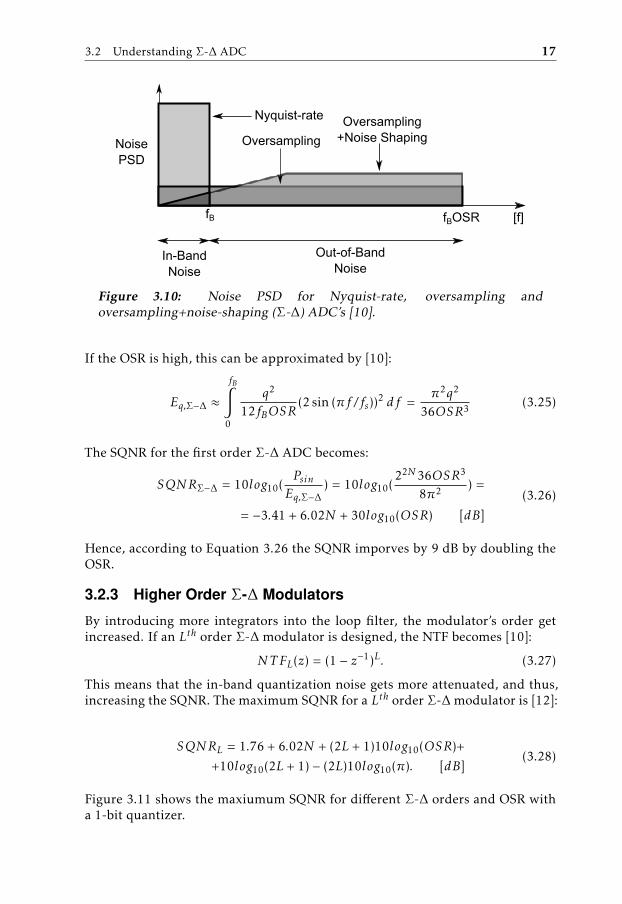
According to Equation 3.22, the STF is a delay element. Equation 3.23 states thatthe NTF has a pole at z = 0 and a zero at z = 1 which corresponds to a high-passfilter. This means that the quantization noise is shaped. Again, the total quan-tization noise remains the same, but it gets pushed to higher frequencies. Thismeans that the in-band quantization noise becomes lower, and thus, the SQNRbecomes larger. This is illustrated in Figure 3.10.
The total in-band noise power for the first order Σ-∆ ADC is:
Eq,Σ−∆ =
fB∫0
Seq ,OS (f )|NT F(z)|2 df =
fB∫0
q2
12fBOSR|1 − e−j2πf /fs |2 df (3.24)
3.2 Understanding Σ-∆ ADC 17
fB
Nyquist-rate
Oversampling
Oversampling+NoiseDShaping
fBOSR [f]
In-BandNoise
Out-of-BandNoise
NoiseDPSD
Figure 3.10: Noise PSD for Nyquist-rate, oversampling andoversampling+noise-shaping (Σ-∆) ADC’s [10].
If the OSR is high, this can be approximated by [10]:
Eq,Σ−∆ ≈
fB∫0
q2
12fBOSR(2 sin (πf /fs))
2 df =π2q2
36OSR3 (3.25)
The SQNR for the first order Σ-∆ ADC becomes:
SQNRΣ−∆ = 10log10(PsinEq,Σ−∆
) = 10log10(22N36OSR3
8π2 ) =
= −3.41 + 6.02N + 30log10(OSR) [dB]
(3.26)
Hence, according to Equation 3.26 the SQNR imporves by 9 dB by doubling theOSR.
3.2.3 Higher Order Σ-∆ Modulators
By introducing more integrators into the loop filter, the modulator’s order getincreased. If an Lth order Σ-∆ modulator is designed, the NTF becomes [10]:
NT FL(z) = (1 − z−1)L. (3.27)
This means that the in-band quantization noise gets more attenuated, and thus,increasing the SQNR. The maximum SQNR for a Lth order Σ-∆ modulator is [12]:
SQNRL = 1.76 + 6.02N + (2L + 1)10log10(OSR)+
+10log10(2L + 1) − (2L)10log10(π). [dB](3.28)
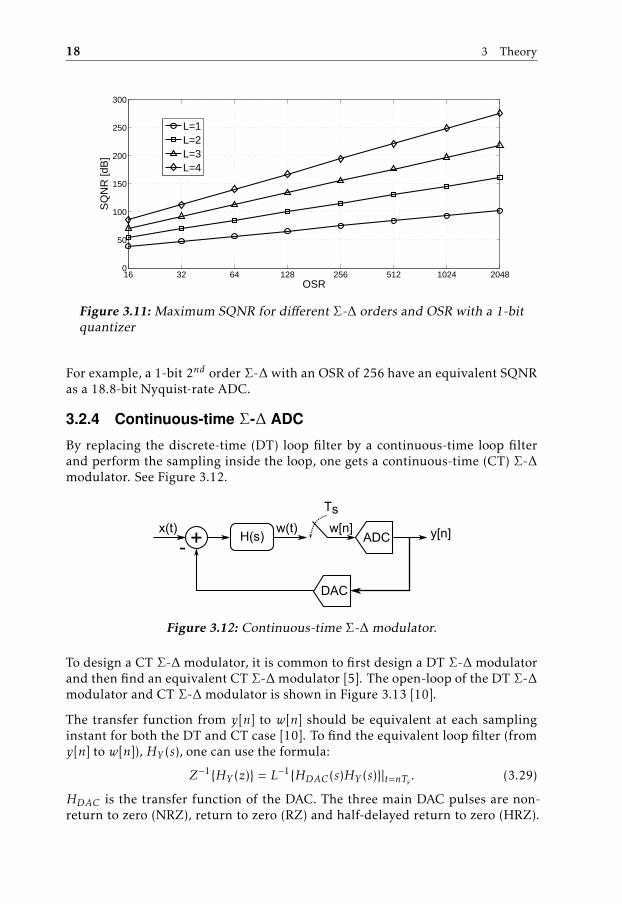
Figure 3.11 shows the maxiumum SQNR for different Σ-∆ orders and OSR witha 1-bit quantizer.
18 3 Theory
16 32 64 128 256 512 1024 20480
50
100
150
200
250
300
OSR
SQ
NR
[dB
]
L=1L=2L=3L=4
Figure 3.11: Maximum SQNR for different Σ-∆ orders and OSR with a 1-bitquantizer
For example, a 1-bit 2nd order Σ-∆ with an OSR of 256 have an equivalent SQNRas a 18.8-bit Nyquist-rate ADC.
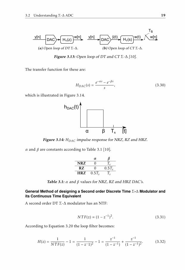
3.2.4 Continuous-time Σ-∆ ADC
By replacing the discrete-time (DT) loop filter by a continuous-time loop filterand perform the sampling inside the loop, one gets a continuous-time (CT) Σ-∆modulator. See Figure 3.12.
+ H(s) ADC
DAC
x(t)
-y[n]
Ts
w(t) w[n]
Figure 3.12: Continuous-time Σ-∆ modulator.
To design a CT Σ-∆ modulator, it is common to first design a DT Σ-∆ modulatorand then find an equivalent CT Σ-∆ modulator [5]. The open-loop of the DT Σ-∆modulator and CT Σ-∆ modulator is shown in Figure 3.13 [10].
The transfer function from y[n] to w[n] should be equivalent at each samplinginstant for both the DT and CT case [10]. To find the equivalent loop filter (fromy[n] to w[n]), HY (s), one can use the formula:
Z−1HY (z) = L−1HDAC(s)HY (s)|t=nTs . (3.29)
HDAC is the transfer function of the DAC. The three main DAC pulses are non-return to zero (NRZ), return to zero (RZ) and half-delayed return to zero (HRZ).
3.2 Understanding Σ-∆ ADC 19
HY(z)DACy[n] w[n]
(a) Open loop of DT Σ-∆.
HY(s)DACy[n]
Ts
w(t) w[n]ŷ(t)
(b) Open loop of CT Σ-∆.
Figure 3.13: Open loop of DT and CT Σ-∆ [10].
The transfer function for these are:
HDAC(s) =e−αs − e−βs
s, (3.30)
which is illustrated in Figure 3.14.
α β Ts [t]
hDAC(t)
Figure 3.14: HDAC impulse response for NRZ, RZ and HRZ.
α and β are constants according to Table 3.1 [10].
α βNRZ 0 TsRZ 0 0.5Ts
HRZ 0.5Ts Ts
Table 3.1: α and β values for NRZ, RZ and HRZ DAC’s.
General Method of designing a Second order Discrete Time Σ-∆ Modulator andits Continuous Time Equivalent
A second order DT Σ-∆ modulator has an NTF:
NT F(z) = (1 − z−1)2. (3.31)
According to Equation 3.20 the loop filter becomes:
H(z) =1
NT F(z)− 1 =
1(1 − z−1)2 − 1 =
z−1
(1 − z−1)+
z−1
(1 − z−1)2 . (3.32)
20 3 Theory
This is shown in Figure 3.15.
+ 11-z-1 + z-1
1-z-1 +X(z)
E(z)
Y(z)W(z)
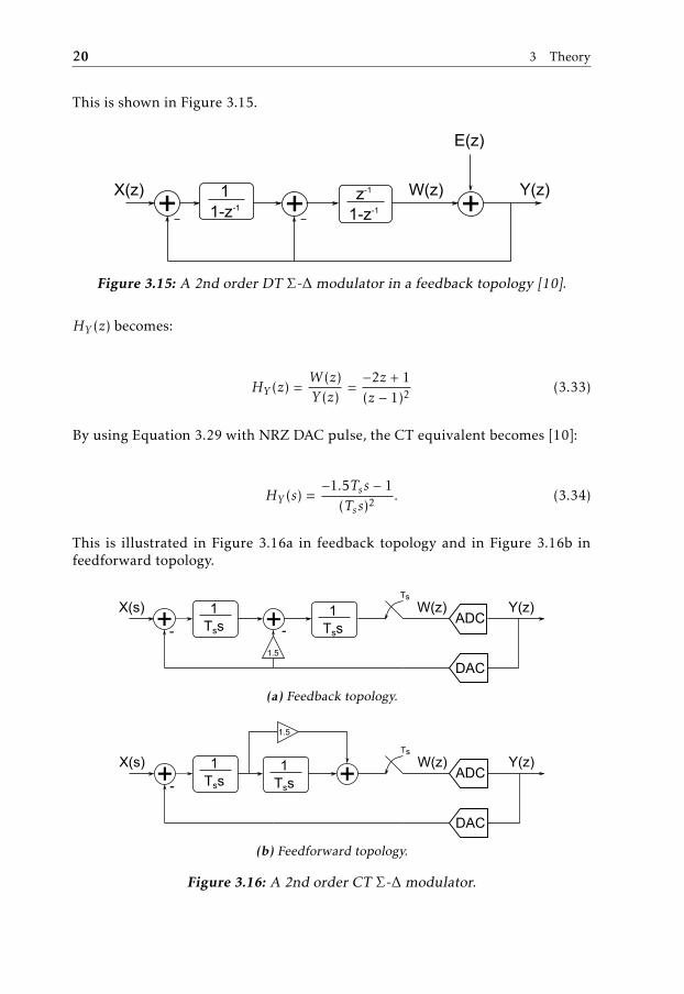
Figure 3.15: A 2nd order DT Σ-∆ modulator in a feedback topology [10].
HY (z) becomes:
HY (z) =W (z)Y (z)
=−2z + 1(z − 1)2 (3.33)
By using Equation 3.29 with NRZ DAC pulse, the CT equivalent becomes [10]:
HY (s) =−1.5Tss − 1
(Tss)2 . (3.34)
This is illustrated in Figure 3.16a in feedback topology and in Figure 3.16b infeedforward topology.
+ 1Tss + 1
Tss
X(s) Y(z)W(z)Ts
1.5
- -ADC
DAC
(a) Feedback topology.
+ 1Tss +1
Tss
X(s) W(z)Ts
1.5
-
(b) Feedforward topology.
Figure 3.16: A 2nd order CT Σ-∆ modulator.

3.2 Understanding Σ-∆ ADC 21
3.2.5 Inherent Anti-Aliasing Filter in CT Σ-∆ ADC
One benefit of the CT Σ-∆ is that it inherits an anti-aliasing filter. This eliminatesan anti-aliasing filter in front of the CT Σ-∆ converter (which is necessary in theDT case). To illustrate this, a modified version of Figure 3.12 is illustrated inFigure 3.17 as in [17].
+ ADC
DAC
X(s)
-Y(z)W(z)
Ts
G(s)
HY(s)
Ts
Figure 3.17: A modified 2nd order CT Σ-∆ converter.
Where,
G(s) =1.5Tss + 1
(Tss)2 (3.35)
and equivalent DT loop filter, HY (z), from Y (z) to W (z) becomes, using Equa-tion 3.29. The NTF becomes [17]:
NT F(z) =1
1 + HY (z). (3.36)
The STF becomes [17]:
ST F(s) = H(s)NT F(esTs ) =G(s)
1 + HY (esTs )(3.37)
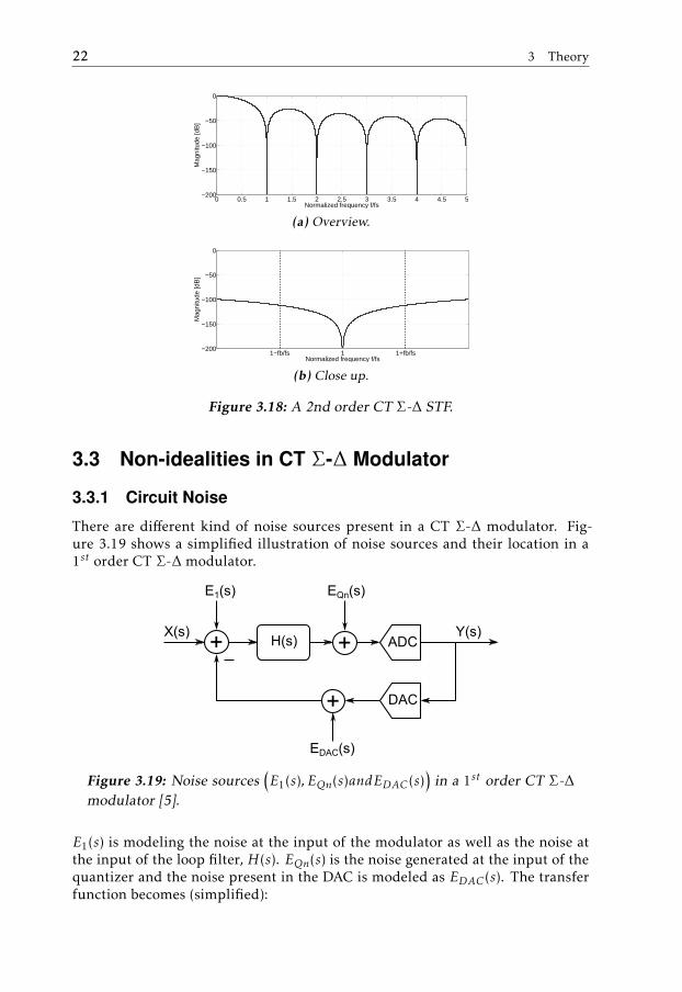
For a NRZ DAC, the STF magnitude response is illustrated in Figure 3.18a.
The signals that can be aliased into the in-band are located within kfs ± fB, wherek is an integer [17]. This is illustrated in Figure 3.18b, where k = 1. One can seethat the aliasing bands are attenuated more than 100dB for a second order CTΣ-∆ modulator, in this example. Therefore, the CT Σ-∆ inherits the anti-aliasingfilter.
22 3 Theory
0 0.5 1 1.5 2 2.5 3 3.5 4 4.5 5−200
−150
−100
−50
0
Mag
nitu
de [d
B]
Normalized frequency f/fs
(a) Overview.
1−fb/fs 1 1+fb/fs−200
−150
−100
−50
0
Mag
nitu
de [d
B]
Normalized frequency f/fs
(b) Close up.
Figure 3.18: A 2nd order CT Σ-∆ STF.
3.3 Non-idealities in CT Σ-∆ Modulator
3.3.1 Circuit Noise
There are different kind of noise sources present in a CT Σ-∆ modulator. Fig-ure 3.19 shows a simplified illustration of noise sources and their location in a1st order CT Σ-∆ modulator.
+ + ADCH(s)X(s)
E1(s) EQn(s)
DAC+
Y(s)
EDAC(s)
Figure 3.19: Noise sources(E1(s), EQn(s)andEDAC(s)
)in a 1st order CT Σ-∆
modulator [5].
E1(s) is modeling the noise at the input of the modulator as well as the noise atthe input of the loop filter, H(s). EQn(s) is the noise generated at the input of thequantizer and the noise present in the DAC is modeled as EDAC(s). The transferfunction becomes (simplified):
3.3 Non-idealities in CT Σ-∆ Modulator 23
Y (s) =X(s)H(s)1 + H(s)
+E1(s)H(s)1 + H(s)
− EDAC(s)H(s)1 + H(s)
+EQn(s)
1 + H(s)=
= ST F(s)[X(s) + E1(s) − HDAC(s)] + NT F(s)EQn(s)(3.38)
According to Equation 3.38 the DAC noise, the input noise and the filter noisewill appear unattenuated at the output in the passband. The noise at the inputof the quantizer, however, will appear at the output shaped like the quantizationnoise. EQn can then be neglected, if the NTF’s attenuation in the passband is highenough. This shows that the location of the noise source is critical regarding thecontribution it got at the output of the modulator.
3.3.2 Excess Loop Delay
Excess loop delay (ELD) is the effect of the delay from the sampling instant ofthe quantizer to the output of the DAC [5]. This can’t be avoided, because of thenon-zero switching time in e.g. transistors. The output of the of a NRZ DAC witha time delay td is illustrated in Figure 3.20.
td Ts Ts+td [t]
Figure 3.20: Output of a NRZ DAC suffering from excess loop delay, withtime delay td .
The ELD effect is dependent on the shape of the DAC [5]. A DAC shape thatis within the sampling period (such as RZ DAC with td < 0.5Ts), results in acoefficient deviation in the loop-filter [5]. For a DAC shape that extends into thenext sampling period (such as NRZ and HRZ DAC’s with td > 0) results in orderincrement of the loop-filter [5]. It is shown by [5, 10] that NRZ DAC suffers moreof ELD compared to RZ. There is almost no degradtion of the CT Σ-∆ modulatorif a RZ DAC is used and td < 0.5Ts [10].
3.3.3 Clock Jitter
Clock jitter is an effect caused by the timing uncertainty of the clock, due to non-idealities. This effect is gaussian and effects the modulator as additional noise[10]. The clock jitter effects both the quantizer and the DAC [5] but, however,the jitter noise introduced in the quantizer is attenuated like the quantizationnoise. The jitter noise introduced in the DAC is not shaped, thus it degrades themodulator. The clock jitter can be seen as variation of the pulse width of the DAC,which corresponds to variation of the amount of feedback charge [15]. The DACis only affected by the clock jitter when it’s switching, therefore the RZ and HRZDACs are affected more by clock jitter compared to NRZ DAC [10]. Another wayto reduce the influence of clock jitter is to use a multibit DAC [15].
24 3 Theory
[t]
Figure 3.21: Illustration of a jittered clock, where the shadows representsthe clock uncertainty area.
3.3.4 Unequal Rise/Fall Time of DAC
Unequal rise and fall times of the DAC is caused by mismatch of the outputcurrent of the DAC [16]. It causes code dependency and this phenomenon iscalled ISI (Inter-Symbol Inteference) [15]. For example: the avarage of the codesc1 = [1, 0, 1, 0] and c2 = [1, 1, 0, 0] should be equal. But with unequal rise andfall times, this is not true. The DAC becomes non linear and will cause distortiontones and additional noise at the output of the ADC [16]. A solution to preventISI is to use a differential DAC or employ RZ of HRZ DAC instead of NRZ DAC[15].
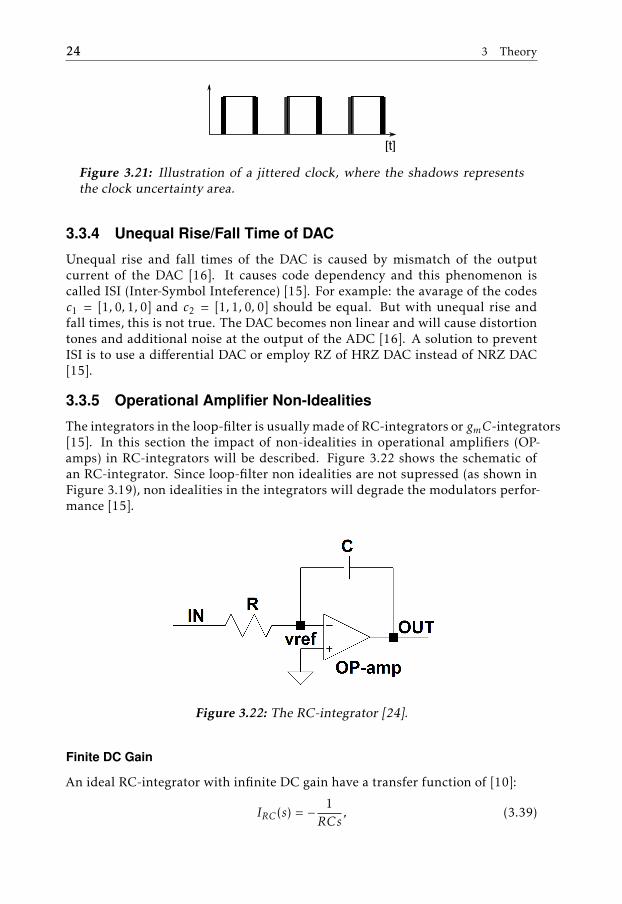
3.3.5 Operational Amplifier Non-Idealities
The integrators in the loop-filter is usually made of RC-integrators or gmC-integrators[15]. In this section the impact of non-idealities in operational amplifiers (OP-amps) in RC-integrators will be described. Figure 3.22 shows the schematic ofan RC-integrator. Since loop-filter non idealities are not supressed (as shown inFigure 3.19), non idealities in the integrators will degrade the modulators perfor-mance [15].
Figure 3.22: The RC-integrator [24].
Finite DC Gain
An ideal RC-integrator with infinite DC gain have a transfer function of [10]:
IRC(s) = − 1RCs
, (3.39)
3.3 Non-idealities in CT Σ-∆ Modulator 25
but, due to finite DC gain (A0) of practical Op-amps, the real transfer functionbecomes [10]:
IRC(s) = − 1RCs
1
1 + (1 + 1RCs )
1A0
. (3.40)
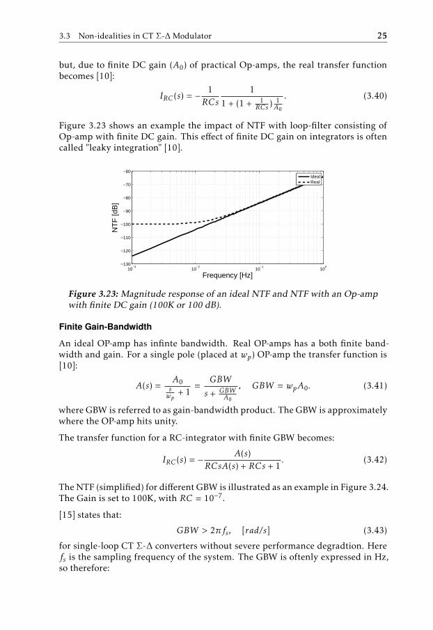
Figure 3.23 shows an example the impact of NTF with loop-filter consisting ofOp-amp with finite DC gain. This effect of finite DC gain on integrators is oftencalled "leaky integration" [10].
10−3
10−2
10−1
100
−130
−120
−110
−100
−90
−80
−70
−60
Frequency [Hz]
NT
F [d
B]
IdealReal
Figure 3.23: Magnitude response of an ideal NTF and NTF with an Op-ampwith finite DC gain (100K or 100 dB).
Finite Gain-Bandwidth
An ideal OP-amp has infinte bandwidth. Real OP-amps has a both finite band-width and gain. For a single pole (placed at wp) OP-amp the transfer function is[10]:
A(s) =A0swp
+ 1=
GBW
s + GBWA0
, GBW = wpA0. (3.41)
where GBW is referred to as gain-bandwidth product. The GBW is approximatelywhere the OP-amp hits unity.
The transfer function for a RC-integrator with finite GBW becomes:
IRC(s) = − A(s)RCsA(s) + RCs + 1
. (3.42)
The NTF (simplified) for different GBW is illustrated as an example in Figure 3.24.The Gain is set to 100K, with RC = 10−7.
[15] states that:
GBW > 2πfs, [rad/s] (3.43)
for single-loop CT Σ-∆ converters without severe performance degradtion. Herefs is the sampling frequency of the system. The GBW is oftenly expressed in Hz,so therefore:

26 3 Theory
10−2
10−1
100
101
102
103
−180
−160
−140
−120
−100
−80
−60
−40
−20
Frequency [Hz]
NT
F [d
B]
IdealGBW=100KHzGBW=800KHzGBW=3MHz
Figure 3.24: NTF for different GBW.
GBW > fs [Hz]. (3.44)
Finite Slew Rate
An other non-ideality in Op-amp (and RC-integrator) is the finite slew rate (SR).Slew rate is due to limited output current, which is intended to charge the ca-pacitor in the RC-integrator. The SR in CT Σ-∆ is relaxed compared to DT Σ-∆,but insufficient SR is causes distortion and additive noise [15]. The easiest wayto determine sufficient SR is by simulation, since different Σ-∆ modulators, DACshapes, etc., influence the SR required and makes it difficult to calculate. There-fore, SR simulation results will be presented in Section 6.2.1.
3.4 Digital Filtering and Decimation
The oversampled data coming from the Σ-∆ modulator need to be filtered anddecimated (lowering the sampling rate) to remove the out-of-band noise and tobe converted down to the Nyquist rate. See Figure 3.25 for an illustration of postprocessing of data from Σ-∆ modulator by filtering and decimation.
R
LP-filter Decimation
fs fs fs/R
Figure 3.25: Low-pass filtering and decimation by a factor R.
Because of the high data rate from the Σ-∆ modulator, the low-pass filter in Fig-ure 3.25 need to operate in fast. Since digital filters often consists of multipliers,this means that the multipliers in the filter need to be very fast and the filter tendto be very long [4]. Eugene B. Hogenauer introduces a class of digital linear phase

3.4 Digital Filtering and Decimation 27
FIR filters for decimation in his paper [6] which doesn’t require any multipliers.This class of filters are called CIC (Cascaded Integrator Comb) filters.
3.4.1 CIC filters
An illustration of a CIC filter is shown in Figure 3.26.
+z-1
+z-1
R +z-M
-+-x[n] y[n]
z-M
1 N 1 N
Integrator section Comb section
Figure 3.26: Illustration of a CIC filter.
The integrator section consists of N number of integrators operating at fs. TheComb section consists of N number of comb filters with differential delay M op-erating at the lower frequency fs/R (where R is the decimation factor). The totalfilter respons becomes [6]:
H(z) = HNI (z)HN
C (z) =(1 − z−RM )N
(1 − z−1)N= [
RM−1∑k=0
z−k]N . (3.45)
The magnitude response can be expressed as [6]:
|H(f )| =
∣∣∣∣∣∣∣sin (πMf )
sin (πfR )
∣∣∣∣∣∣∣N
. (3.46)
The differential delay, M, is chosen to be usually 1 or 2 [6]. See Figure 3.27 forthe frequency response relative to the low (decimated) sampling frequency of theCIC filter for different filter orders.
One can see that the a zero is placed at every multiple of the low (decimated)frequency. A region around every multiple of the decimated frequency is foldedback into the passband, causing aliasing [6]. The region is 2fB wide, where fB isthe passband frequency relative to the low sampling rate. The maximum aliasingerror is usually at the lower edge of the first aliasing band 1−fB [6]. In Figure 3.27this is approximatly 17.1dB, 34.3dB, 51.4dB, 68.5dB and 85.6dB for N = 1 . . . 5,respectively. When designing the CIC filter, this has to be taken into account aswell as the passband droop at fB.
To overcome the poor passband droop and the aliasing band characteristics, onecan use CIC filters to make transition from high to low sampling rates, with adecimation factor R1, and then use conventional filters to shape the frequency

28 3 Theory
0 fb 0.5 1−fb 1 1+fb 1.5 2−fb 2 2+fb 2.5−140
−120
−100
−80
−60
−40
−20
0
Frequency relative to low sampling frequency
Mag
nitu
de [d
B]
N=1N=2N=3N=4N=5
Figure 3.27: Magnitude respons for different filter order vs. frequency rela-tive to the low (decimated) sampling frequency, where R = 256 and M = 1.fB is 1/8 relative to the low sampling frequency.
response and decimate by a factor R2. This is illustrated in Figure 3.28. The totaldecimation factor is R = R1R2.
R2
LP-filter DecimationCIC filter
fs fs/R1 fs/R
Figure 3.28: CIC filter decimation by a factor R1 and conventional decima-tion filter by a factor R2, where R = R1 × R2.
Hogenauer [6] states that the gain of the CIC filter is simply:
G = (RM)N , (3.47)
where R is the decimation factor, M is the differential delay in the Comb sectionsand N is the order of the CIC filter. To be sure that the registers don’t overflow,the register width has to be at least [6]:
BOUT = Nlog2(RM) + BIN − 1, (3.48)
where BIN is the number of bits in the input data stream, where the LSB is con-sidered to be bit zero. For an 1-bit input data stream with R = 64, M = 1 andN = 5, the register widths have to be at least 31 bits long.

4Test Setup
This chapter is describing how the converters are tested. The converters consistsof external components and an FPGA, which are mounted on a PCB. There willalso be a section about the test setup quality (Section 4.2).
4.1 Test Setup
The test setup is illustrated in Figure 4.1. The PC generates a sine wave whichis sent to an external sound card, the M-Audio Fast Track Pro. The sound cardis then genereting an analog signal of the sine wave which is sent to the DUT(Device Under Test). The DUT is the converter under test, which is a PCB with theFPGA and external components. The result of the A/D-convertion, generated bythe DUT, is then fed back to the sound card using S/PDIF with 24 bits resolution,which is then recorded by the PC. The collected data is analyzed in Matlab.
DUT Power Supply
Analog
Digital
M-AudioFast Track ProPC
Figure 4.1: Test setup for testing the converter.
The sound card (M-Audio Fast Track Pro) claims to be a 103dB SNR and 86 dBSNDR DAC [14].
29

30 4 Test Setup
4.2 Control of Test Setup Quality
To control if the sound card have the claimed SNR and SNDR, this section willpresent results of the sound card only. This is done by using the sound card inloop-back, i.e. feeding an analog output and recording it with the analog inputof the sound card (ADC). The built in ADC claims to have a 101 dB SNR and 86dB SNDR [14]. An FFT plot of the recorded signal is shown in Figure 4.2.
0 0.1 0.2 0.3 0.4 0.5−160
−140
−120
−100
−80
−60
−40
−20
0
Frequency [ f / fs ]
PS
D [
dB
]
SNR = 88.8dB SNDR = 86.1dB THD = −89.4dB SFDR = 90.8dB ENOB = 14.01bits
H2 = −91.7dBFS
H3 = −95.8dBFS
H4 = −137.6dBFSH
5 = −135.3dBFS
H6 = −151.3dBFS
H7 = −135.0dBFS H
8 = −138.6dBFS H
9 = −137.0dBFS
H10
= −143.1dBFS
H1 = −0.9dBFS
Figure 4.2: 65536 point FFT of the output of the M-Audio Fast Track Pro,using a -1dBFS and ∼7.3KHz input signal. The SNDR is verified (86 dB), butthe SNR is much lower than the stated 103 dB.
SNDR/SNR vs. input frequency is shown in Figure 4.3.
0 0.05 0.1 0.15 0.2 0.25 0.3 0.35 0.4 0.45 0.581
81.5
82
82.5
83
83.5
84
84.5
85
Relative Frequency f/fOUT
SN
R/S
ND
R [d
B]
SNRSNDR
Figure 4.3: SNR/SNDR vs. frequency of M-Audio Fast Track Pro, using a-6dBFS input signal.
SNDR/SNR vs. input amplitude is shown in Figure 4.4.
4.2 Control of Test Setup Quality 31
−80 −70 −60 −50 −40 −30 −20 −10 00
10
20
30
40
50
60
70
80
90
100
Input Amplitude [dBFS]
SN
R/S
ND
R [d
B]
SNRSNDR
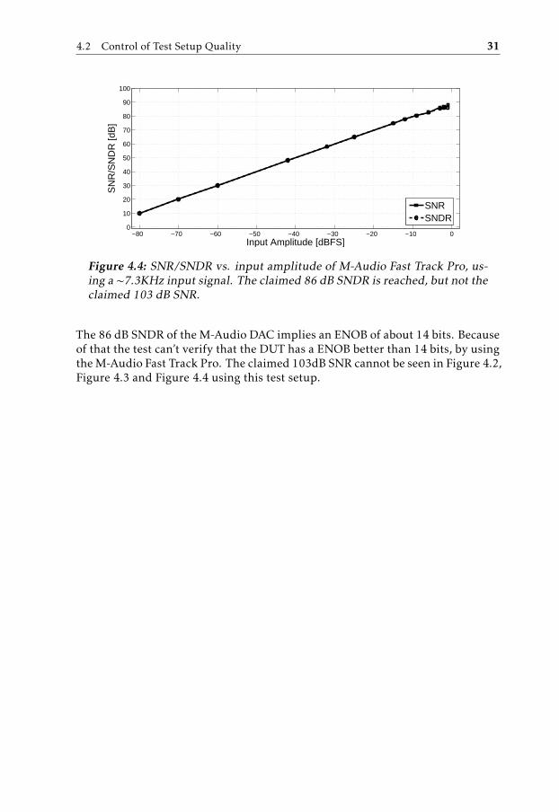
Figure 4.4: SNR/SNDR vs. input amplitude of M-Audio Fast Track Pro, us-ing a ∼7.3KHz input signal. The claimed 86 dB SNDR is reached, but not theclaimed 103 dB SNR.
The 86 dB SNDR of the M-Audio DAC implies an ENOB of about 14 bits. Becauseof that the test can’t verify that the DUT has a ENOB better than 14 bits, by usingthe M-Audio Fast Track Pro. The claimed 103dB SNR cannot be seen in Figure 4.2,Figure 4.3 and Figure 4.4 using this test setup.

5Implementation of a Passive Σ-∆
Converter
This chapter will describe the implementation of a low-cost passive Σ-∆ con-verter. First there will be a section about the system overview (Section 5.1).Thereafter there will be a section about the implementation of the modulatoritself (Section 5.2), a section about the CIC filter (Section 5.3) and a section aboutthe FIR filter (Section 5.4). Section 5.5 presents the results. In the last section(Section 5.6) there will be a discussion of the results of the passive Σ-∆ converter.
5.1 System Overview
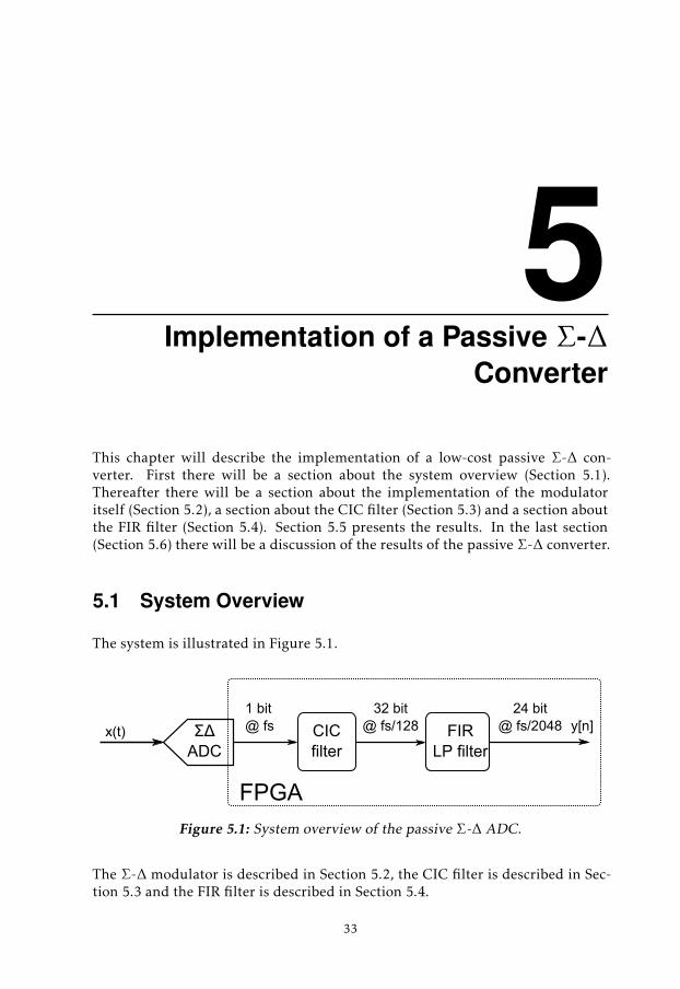
The system is illustrated in Figure 5.1.
x(t) ΣΔADC
CICfilter
FIRLPnfilter
1nbit@nfs
32nbit@nfs/128
24nbit@nfs/2048
FPGA
y[n]
Figure 5.1: System overview of the passive Σ-∆ ADC.
The Σ-∆ modulator is described in Section 5.2, the CIC filter is described in Sec-tion 5.3 and the FIR filter is described in Section 5.4.
33
34 5 Implementation of a Passive Σ-∆ Converter
Specification Symbol ValueSampling frequency fs 98.304MHzOversampling ratio OSR 2048
Output sampling rate fOUT 48KS/sSupply voltage V dd 3.3V single supply
Input bandwidth fB 20KHzInput voltage amplitude (max) Ain 1.65 V
Table 5.1: Specification for the passive Σ-∆ ADC.
5.2 The Passive Σ-∆ Modulator
In order to cut the cost of a Σ-∆ ADC, the loop-filter consists only of passivecomponents. The loop-filter of a typical (active) Σ-∆ is employing integratorswith high gain (e.g. RC-integrators). One can make an integrator of passive com-ponents with e.g. a RC-filter, a so called "lossy integrator" with no gain. Thelinearization of the passive Σ-∆ is shown in Figure 5.2. The gain G is the gainof the quantizer/comparator [3], which in Figure 3.9 is assumed to be small andnegligible.
X(z)+-
Y(z)+
E(z)
H(z) G
Figure 5.2: Linearization of the passive Σ-∆ ADC.
The transfer function becomes:
Y (z) =GH(z)
1 + GH(z)X(z) +
11 + GH(z)
E(z) (5.1)
The gain factor G is assumed to be constant. [3] estimates the value of G bynulling the input, x. The 1-bit output, y[n], will alternate (ideally) between 0and 1 at a rate of fs/2. This signal is then passed to the (low-pass) loop filter bya DAC. If the sampling frequency is high enough the signal is attenuated by afactor |H(f = fs/2)|, and this G is roughly:
G ≈ 1|H(f = fs/2)|
. (5.2)
5.2 The Passive Σ-∆ Modulator 35
A first order RC-filter with transfer function:
H(s) =1
RCs + 1=
1swp
+ 1. (5.3)
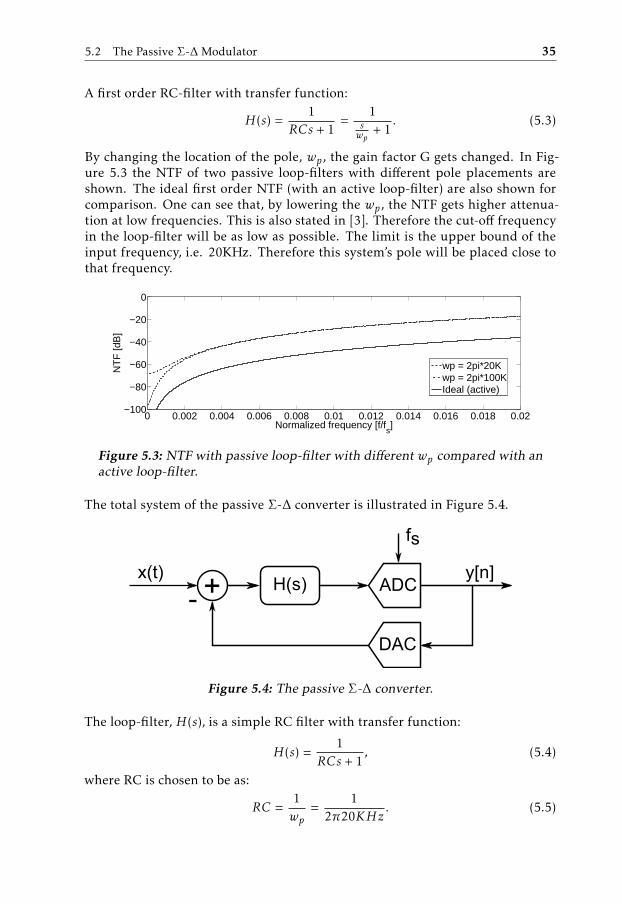
By changing the location of the pole, wp, the gain factor G gets changed. In Fig-ure 5.3 the NTF of two passive loop-filters with different pole placements areshown. The ideal first order NTF (with an active loop-filter) are also shown forcomparison. One can see that, by lowering the wp, the NTF gets higher attenua-tion at low frequencies. This is also stated in [3]. Therefore the cut-off frequencyin the loop-filter will be as low as possible. The limit is the upper bound of theinput frequency, i.e. 20KHz. Therefore this system’s pole will be placed close tothat frequency.
0 0.002 0.004 0.006 0.008 0.01 0.012 0.014 0.016 0.018 0.02−100
−80
−60
−40
−20
0
Normalized frequency [f/fs]
NT
F [d
B]
wp = 2pi*20Kwp = 2pi*100KIdeal (active)
Figure 5.3: NTF with passive loop-filter with different wp compared with anactive loop-filter.
The total system of the passive Σ-∆ converter is illustrated in Figure 5.4.
x(t)+-
H(s) ADC
DAC
fs
y[n]
Figure 5.4: The passive Σ-∆ converter.
The loop-filter, H(s), is a simple RC filter with transfer function:
H(s) =1
RCs + 1, (5.4)
where RC is chosen to be as:
RC =1wp
=1
2π20KHz. (5.5)

36 5 Implementation of a Passive Σ-∆ Converter
The ADC in Figure 5.4 is chosen to be a 1-bit quantizer, employing the LVDSbuffer in the FPGA, sampled at fs = 98.304MHz.
The DAC is chosen to be a 1 bit DAC, which only uses one pin on the FPGA.Figure 5.5 illustrates the 1-bit DAC. Here, the output of the FPGA is chosen tobe a tri-state buffer and therefore the output of the DAC can either be Vdd, GNDor T. This tri-state buffer can be used to create NRZ, RZ and HRZ DAC pulses. Tstands for tri-state and is a high output impedence state (no current can flow outof the FPGA). NRZ pulses is either "high" or "low" for the whole sample period,i.e., it doesn’t employ the T-state. On the other hand, the T-state can be usedto implement RZ and HRZ pulses which is "off" for half of the sample period.One thing to take into account is the parasitic capacitance assosiated with thepad, Cp. This capacitance is max 10pF [26]. This implies that the time constant,RDACCp, has to be as low as possible, in order to get the same shape as illustratedin Figure 3.14.
+Vdd
GND
T
1-bit DAC
To loop-filterPAD
Cp
y[n]ŷ(t)
From FPGA
RDAC
Figure 5.5: Simple illustration of an 1-bit DAC.
The chosen 1-bit DAC will use NRZ pulses because of the simplicity and "mini-mal" impact of the parasitic capacitance.
The converter is therefore only using three pins on the FPGA: two for the LVDSbuffer and one for the NRZ DAC.
5.2.1 Realization of the Passive Σ-∆ Converter
Figure 5.6 illustrates the realization of the Σ-∆ converter. The 1-bit digital outwill be further processed (filtered and decimated) by the CIC and FIR filter. Thereference signal (vref) is mid-range, i.e. V dd/2 = 1.65V .
The chosen component values are presented in Table 5.2.
Component ValueRIN 6.8KΩRDAC 6.8KΩC 1nFR 6.8KΩCIN 1µF
Table 5.2: Component values for the passive Σ-∆ modulator.

5.2 The Passive Σ-∆ Modulator 37
Figure 5.6: Realization of the passive Σ-∆ converter [13].
5.2.2 Simulation Results
The simulation was done using Simulink/Matlab with the passive modulator il-lustrated in Figure 5.4. The filtering and decimation used in this simulation are"ideal", in order to characterize the Σ-∆ modulator only. Figure 5.7 shows an FFTplot of the output of the modulator.
0 0.1 0.2 0.3 0.4 0.5−160
−140
−120
−100
−80
−60
−40
−20
0
Frequency [ f / fs ]
PS
D [
dB
]
SNR = 90.3dB SNDR = 90.2dB THD = −106.8dB SFDR = 111.0dB ENOB = 14.70bits
H2 = −129.2dBFS
H3 = −115.5dBFSH
4 = −116.6dBFSH
5 = −117.5dBFSH
6 = −118.6dBFS
H7 = −111.0dBFS
H8 = −125.9dBFS
H9 = −115.1dBFS
H10
= −118.9dBFS
H1 = −0.0dBFS
Figure 5.7: 1024 point FFT plot of the output of the passive Σ-∆ modualtor.The input signal is 2KHz and has an amplitude of 1V.
Figure 5.8 shows the SNDR/SNR vs. input frequency.

38 5 Implementation of a Passive Σ-∆ Converter
0 0.05 0.1 0.15 0.2 0.25 0.3 0.35 0.4 0.4588
89
90
91
92
93
94
Relative Frequency f/fOUT
SN
R/S
ND
R [d
B]
SNDRSNR
Figure 5.8: SNDR and SNR vs. Input Frequency. Using a 1V input signal.
5.2.3 Non-idealities in the Passive Σ-∆ modulator
Hysteresis
Because the noise transfer function (NTF) of the passive Σ-∆ doesn’t have highattenuation in the passband, the hysteresis of the comparator can’t be neglected.See Section 2.2.1 for the defenition of hysteresis of a comparator. See Figure 5.9for simulation results of the passive Σ-∆ modulator(illustrated in Figure 5.6) us-ing "ideal" filtering and decimation.
0 0.1 0.2 0.3 0.4 0.5−160
−140
−120
−100
−80
−60
−40
−20
0
Frequency [ f / fs ]
PS
D [
dB
]
SNR = 90.3dB SNDR = 90.2dB THD = −106.8dB SFDR = 111.0dB ENOB = 14.70bits
H2 = −129.2dBFS
H3 = −115.5dBFSH
4 = −116.6dBFSH
5 = −117.5dBFSH
6 = −118.6dBFS
H7 = −111.0dBFS
H8 = −125.9dBFS
H9 = −115.1dBFS
H10
= −118.9dBFS
H1 = −0.0dBFS
(a) 0mV hysteresis.
0 0.1 0.2 0.3 0.4 0.5−160
−140
−120
−100
−80
−60
−40
−20
0
Frequency [ f / fs ]
PS
D [
dB
]
SNR = 74.0dB SNDR = 72.3dB THD = −77.1dB SFDR = 78.6dB ENOB = 11.71bits
H2 = −104.4dBFS
H3 = −78.6dBFS
H4 = −103.8dBFS
H5 = −85.3dBFS
H6 = −111.8dBFS
H7 = −94.4dBFS
H8 = −107.2dBFS
H9 = −86.6dBFS
H10
= −100.9dBFS
H1 = −0.0dBFS
(b) 30 mV hysteresis.
Figure 5.9: Hysteresis effect of the comparator in the passive Σ-∆ modulatorwith "ideal" filtering and decimation. Using 1024 point FFT, with Hanningwindow and ∼2KHz input signal with amplitude of 1V.
One can see that the noise floor increases and distortion is generated due to the
5.3 The CIC filter 39
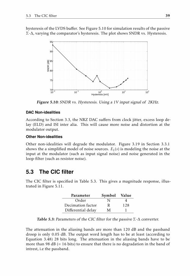
hysteresis of the LVDS buffer. See Figure 5.10 for simulation results of the passiveΣ-∆, varying the comparator’s hysteresis. The plot shows SNDR vs. Hysteresis.
10−2
10−1
100
101
10270
75
80
85
90
95
Hysteresis [mV]
SN
DR
[dB
]
Figure 5.10: SNDR vs. Hysteresis. Using a 1V input signal of 2KHz.
DAC Non-idealities
According to Section 3.3, the NRZ DAC suffers from clock jitter, excess loop de-lay (ELD) and ISI inter alia. This will cause more noise and distortion at themodulator output.
Other Non-idealities
Other non-idealities will degrade the modulator. Figure 3.19 in Section 3.3.1shows the a simplified model of noise sources. E1(s) is modeling the noise at theinput at the modulator (such as input signal noise) and noise generated in theloop-filter (such as resistor noise).
5.3 The CIC filter
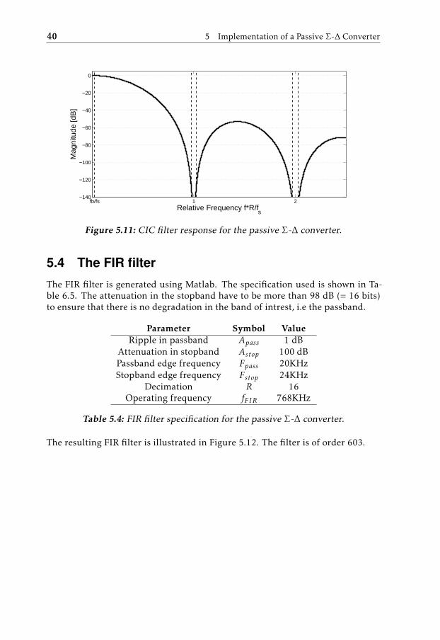
The CIC filter is specified in Table 5.3. This gives a magnitude response, illus-trated in Figure 5.11.
Parameter Symbol ValueOrder N 4
Decimation factor R 128Differential delay M 1
Table 5.3: Parameters of the CIC filter for the passive Σ-∆ converter.
The attenuation in the aliasing bands are more than 120 dB and the passbanddroop is only 0.05 dB. The output word length has to be at least (according toEquation 3.48) 28 bits long. The attenuation in the aliasing bands have to bemore than 98 dB (= 16 bits) to ensure that there is no degradation in the band ofintrest, i.e the passband.
40 5 Implementation of a Passive Σ-∆ Converter
fb/fs 1 2−140
−120
−100
−80
−60
−40
−20
0
Relative Frequency f*R/fs
Mag
nitu
de [d
B]
Figure 5.11: CIC filter response for the passive Σ-∆ converter.
5.4 The FIR filter
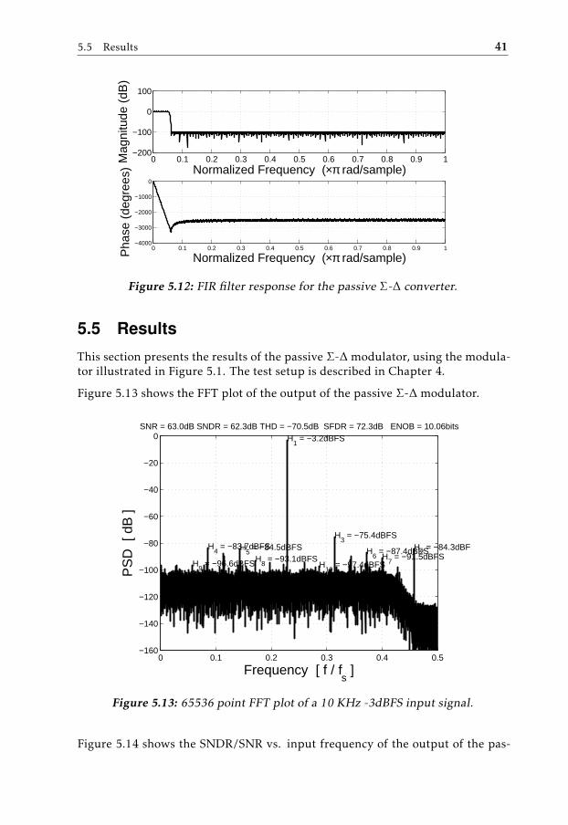
The FIR filter is generated using Matlab. The specification used is shown in Ta-ble 6.5. The attenuation in the stopband have to be more than 98 dB (= 16 bits)to ensure that there is no degradation in the band of intrest, i.e the passband.
Parameter Symbol ValueRipple in passband Apass 1 dB
Attenuation in stopband Astop 100 dBPassband edge frequency Fpass 20KHzStopband edge frequency Fstop 24KHz
Decimation R 16Operating frequency fFIR 768KHz
Table 5.4: FIR filter specification for the passive Σ-∆ converter.
The resulting FIR filter is illustrated in Figure 5.12. The filter is of order 603.
5.5 Results 41
0 0.1 0.2 0.3 0.4 0.5 0.6 0.7 0.8 0.9 1−4000
−3000
−2000
−1000
0
Normalized Frequency (×π rad/sample)Pha
se (
degr
ees)
0 0.1 0.2 0.3 0.4 0.5 0.6 0.7 0.8 0.9 1−200
−100
0
100
Normalized Frequency (×π rad/sample)
Mag
nitu
de (
dB)
Figure 5.12: FIR filter response for the passive Σ-∆ converter.
5.5 Results
This section presents the results of the passive Σ-∆ modulator, using the modula-tor illustrated in Figure 5.1. The test setup is described in Chapter 4.
Figure 5.13 shows the FFT plot of the output of the passive Σ-∆ modulator.
0 0.1 0.2 0.3 0.4 0.5−160
−140
−120
−100
−80
−60
−40
−20
0
Frequency [ f / fs ]
PS
D [
dB
]
SNR = 63.0dB SNDR = 62.3dB THD = −70.5dB SFDR = 72.3dB ENOB = 10.06bits
H2 = −84.3dBFS
H3 = −75.4dBFS
H4 = −83.7dBFSH
5 = −84.5dBFS H
6 = −87.4dBFS
H7 = −91.5dBFSH
8 = −93.1dBFSH
9 = −96.6dBFS H
10 = −97.4dBFS
H1 = −3.2dBFS
Figure 5.13: 65536 point FFT plot of a 10 KHz -3dBFS input signal.
Figure 5.14 shows the SNDR/SNR vs. input frequency of the output of the pas-
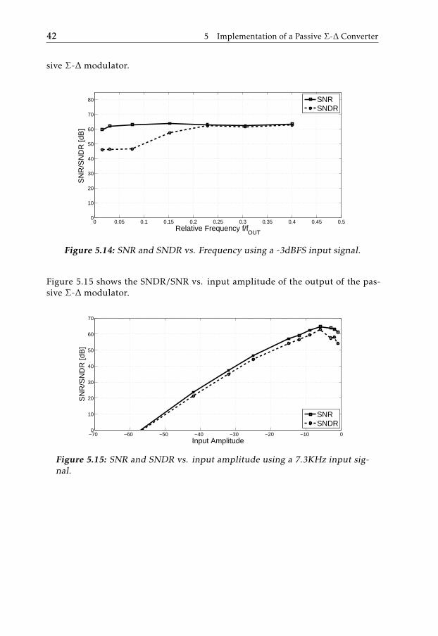
42 5 Implementation of a Passive Σ-∆ Converter
sive Σ-∆ modulator.
0 0.05 0.1 0.15 0.2 0.25 0.3 0.35 0.4 0.45 0.50
10
20
30
40
50
60
70
80
Relative Frequency f/fOUT
SN
R/S
ND
R [d
B]
SNRSNDR
Figure 5.14: SNR and SNDR vs. Frequency using a -3dBFS input signal.
Figure 5.15 shows the SNDR/SNR vs. input amplitude of the output of the pas-sive Σ-∆ modulator.
−70 −60 −50 −40 −30 −20 −10 00
10
20
30
40
50
60
70
Input Amplitude
SN
R/S
ND
R [d
B]
SNRSNDR
Figure 5.15: SNR and SNDR vs. input amplitude using a 7.3KHz input sig-nal.
5.6 Discussion 43
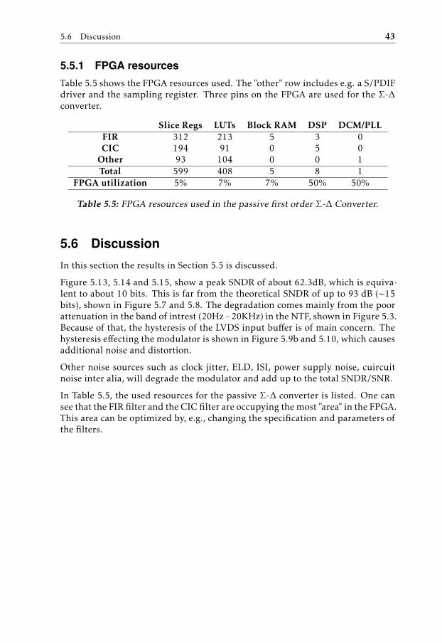
5.5.1 FPGA resources
Table 5.5 shows the FPGA resources used. The "other" row includes e.g. a S/PDIFdriver and the sampling register. Three pins on the FPGA are used for the Σ-∆converter.
Slice Regs LUTs Block RAM DSP DCM/PLLFIR 312 213 5 3 0CIC 194 91 0 5 0
Other 93 104 0 0 1Total 599 408 5 8 1
FPGA utilization 5% 7% 7% 50% 50%
Table 5.5: FPGA resources used in the passive first order Σ-∆ Converter.
5.6 Discussion
In this section the results in Section 5.5 is discussed.
Figure 5.13, 5.14 and 5.15, show a peak SNDR of about 62.3dB, which is equiva-lent to about 10 bits. This is far from the theoretical SNDR of up to 93 dB (∼15bits), shown in Figure 5.7 and 5.8. The degradation comes mainly from the poorattenuation in the band of intrest (20Hz - 20KHz) in the NTF, shown in Figure 5.3.Because of that, the hysteresis of the LVDS input buffer is of main concern. Thehysteresis effecting the modulator is shown in Figure 5.9b and 5.10, which causesadditional noise and distortion.
Other noise sources such as clock jitter, ELD, ISI, power supply noise, cuircuitnoise inter alia, will degrade the modulator and add up to the total SNDR/SNR.
In Table 5.5, the used resources for the passive Σ-∆ converter is listed. One cansee that the FIR filter and the CIC filter are occupying the most "area" in the FPGA.This area can be optimized by, e.g., changing the specification and parameters ofthe filters.

6Implementation of a Second Order
Σ-∆ Converter
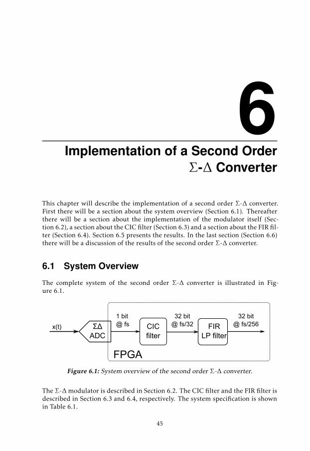
This chapter will describe the implementation of a second order Σ-∆ converter.First there will be a section about the system overview (Section 6.1). Thereafterthere will be a section about the implementation of the modulator itself (Sec-tion 6.2), a section about the CIC filter (Section 6.3) and a section about the FIR fil-ter (Section 6.4). Section 6.5 presents the results. In the last section (Section 6.6)there will be a discussion of the results of the second order Σ-∆ converter.
6.1 System Overview
The complete system of the second order Σ-∆ converter is illustrated in Fig-ure 6.1.
x(t) ΣΔADC
CICfilter
FIRLP filter
1 bit@ fs
32 bit@ fs/32
32 bit@ fs/256
FPGA
Figure 6.1: System overview of the second order Σ-∆ converter.
The Σ-∆ modulator is described in Section 6.2. The CIC filter and the FIR filter isdescribed in Section 6.3 and 6.4, respectively. The system specification is shownin Table 6.1.
45
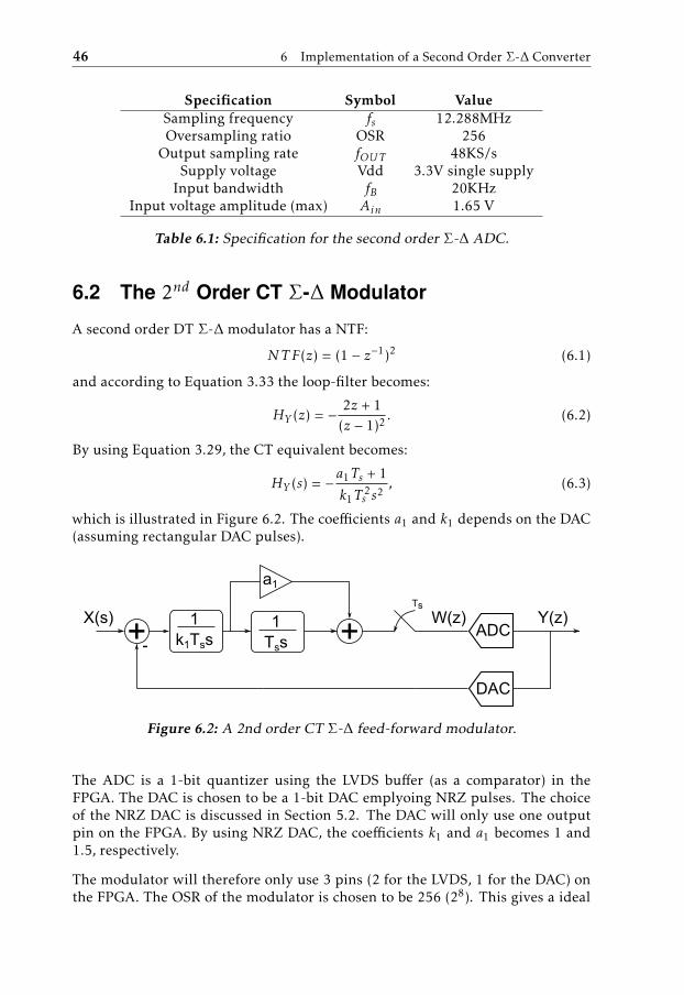
46 6 Implementation of a Second Order Σ-∆ Converter
Specification Symbol ValueSampling frequency fs 12.288MHzOversampling ratio OSR 256
Output sampling rate fOUT 48KS/sSupply voltage Vdd 3.3V single supply
Input bandwidth fB 20KHzInput voltage amplitude (max) Ain 1.65 V
Table 6.1: Specification for the second order Σ-∆ ADC.
6.2 The 2nd Order CT Σ-∆ Modulator
A second order DT Σ-∆ modulator has a NTF:
NT F(z) = (1 − z−1)2 (6.1)
and according to Equation 3.33 the loop-filter becomes:
HY (z) = − 2z + 1(z − 1)2 . (6.2)
By using Equation 3.29, the CT equivalent becomes:
HY (s) = −a1Ts + 1
k1T2s s2
, (6.3)
which is illustrated in Figure 6.2. The coefficients a1 and k1 depends on the DAC(assuming rectangular DAC pulses).
+ 1k1Tss +1
Tss
X(s) W(z)Ts
-
a1
Figure 6.2: A 2nd order CT Σ-∆ feed-forward modulator.
The ADC is a 1-bit quantizer using the LVDS buffer (as a comparator) in theFPGA. The DAC is chosen to be a 1-bit DAC emplyoing NRZ pulses. The choiceof the NRZ DAC is discussed in Section 5.2. The DAC will only use one outputpin on the FPGA. By using NRZ DAC, the coefficients k1 and a1 becomes 1 and1.5, respectively.
The modulator will therefore only use 3 pins (2 for the LVDS, 1 for the DAC) onthe FPGA. The OSR of the modulator is chosen to be 256 (28). This gives a ideal
6.2 The 2nd Order CT Σ-∆ Modulator 47
SQNR, derived from Equation 3.28, of:
SQNR = 1.76 + 6.02 + 50log10(256) + 10log10(5) − 4log10(π) ≈ 115[dB]. (6.4)
That is equal to a 18.8 bits Nyquist-rate ADC.
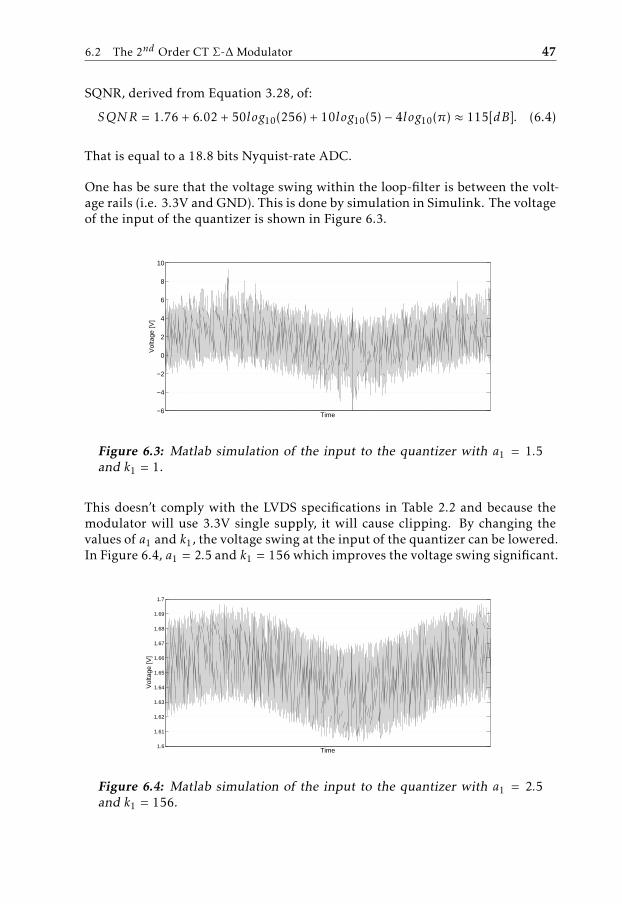
One has be sure that the voltage swing within the loop-filter is between the volt-age rails (i.e. 3.3V and GND). This is done by simulation in Simulink. The voltageof the input of the quantizer is shown in Figure 6.3.
−6
−4
−2
0
2
4
6
8
10
Time
Vol
tage
[V]
Figure 6.3: Matlab simulation of the input to the quantizer with a1 = 1.5and k1 = 1.
This doesn’t comply with the LVDS specifications in Table 2.2 and because themodulator will use 3.3V single supply, it will cause clipping. By changing thevalues of a1 and k1, the voltage swing at the input of the quantizer can be lowered.In Figure 6.4, a1 = 2.5 and k1 = 156 which improves the voltage swing significant.
1.6
1.61
1.62
1.63
1.64
1.65
1.66
1.67
1.68
1.69
1.7
Time
Vol
tage
[V]
Figure 6.4: Matlab simulation of the input to the quantizer with a1 = 2.5and k1 = 156.

48 6 Implementation of a Second Order Σ-∆ Converter
6.2.1 Realization of the 2nd order CT Σ-∆ modulator
The realization of the modulator is shown in Figure 6.5. The loop-filter is a singleamplifier section, derived from [24], chapter 6.5. This loop-filter only use one OPamplifier, which is better than two in a low-cost perspective.
Figure 6.5: Realization of the 2nd order CT Σ-∆ modulator.
The reference voltage is mid-range, i.e. Vdd /2 = 1.65V and is generated by avoltage divider with two resistors. The transfer function from the DAC to theinput of the LVDS buffer is:
HY (s) = −R1(C1 + C2)s + 1RDACR1C1C2s2
= −a1Tss + 1
k1T2s s2
, (6.5)
where
R1(C1 + C2) = a1Ts (6.6)
RDACR1C1C2 = k1T2s (6.7)
Table 6.2 shows the chosen component values. The chosen component valuescorresponds to a1 ≈ 2.5 and k1 ≈ 156.
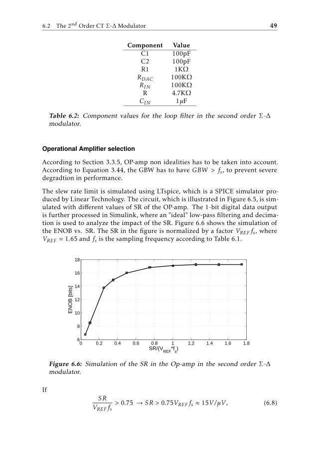
6.2 The 2nd Order CT Σ-∆ Modulator 49
Component ValueC1 100pFC2 100pFR1 1KΩ
RDAC 100KΩ
RIN 100KΩ
R 4.7KΩ
CIN 1µF
Table 6.2: Component values for the loop filter in the second order Σ-∆modulator.
Operational Amplifier selection
According to Section 3.3.5, OP-amp non idealities has to be taken into account.According to Equation 3.44, the GBW has to have GBW > fs, to prevent severedegradtion in performance.
The slew rate limit is simulated using LTspice, which is a SPICE simulator pro-duced by Linear Technology. The circuit, which is illustrated in Figure 6.5, is sim-ulated with different values of SR of the OP-amp. The 1-bit digital data outputis further processed in Simulink, where an "ideal" low-pass filtering and decima-tion is used to analyze the impact of the SR. Figure 6.6 shows the simulation ofthe ENOB vs. SR. The SR in the figure is normalized by a factor VREFfs, whereVREF = 1.65 and fs is the sampling frequency according to Table 6.1.
0 0.2 0.4 0.6 0.8 1 1.2 1.4 1.6 1.86
8
10
12
14
16
18
SR/(VREF
*fs)
EN
OB
[bits
]
Figure 6.6: Simulation of the SR in the Op-amp in the second order Σ-∆modulator.
IfSR
VREFfs> 0.75 → SR > 0.75VREFfs ≈ 15V /µV , (6.8)

50 6 Implementation of a Second Order Σ-∆ Converter
there is almost no degradtion of the modulator.
Table 6.3 summarizes the OP-amp specification.
Specification Symbol ValueDC Gain A0 100K (100dB)
Gain Bandwith Product (min) GBW 12.288 MHzSlew Rate (min) SR 15 V /µV
Table 6.3: OP-amp specifications.
The Op-amp is chosen to be LMV793, which is a low-noise operational amplifierwith 88MHz GBW, 32/24 V /µV SR and approximately 100dB DC Gain [22]. Thechosen Op-amp met the specification in Table 6.3.
6.2.2 Simulation Results
The simulation was done using LTspice and Simulink/Matlab. LTspice simulatedthe Σ-∆ modulator, while Simulink/Matlab simulated an "ideal" filter and dec-imation. Figure 6.7 shows an FFT plot of the second order converter and Fig-ure 6.8 shows SNR/SNDR vs. frequency of the output of the converter.
0 0.1 0.2 0.3 0.4 0.5−160
−140
−120
−100
−80
−60
−40
−20
0
Frequency [ f / fs ]
PS
D [
dB
]
SNR = 100.1dB SNDR = 98.5dB THD = −103.6dB SFDR = 106.2dB ENOB = 16.07bits
H2 = −142.6dBFS
H3 = −110.6dBFS
H4 = −136.0dBFS
H5 = −114.8dBFS
H6 = −120.5dBFSH
7 = −118.3dBFSH
8 = −121.8dBFSH
9 = −120.2dBFS
H10
= −134.8dBFS
H1 = −4.3dBFS
Figure 6.7: Simulation result of the second order Σ-∆ modulator using 1024points FFT, 1V input amplitude (-4.3 dBFS).

6.2 The 2nd Order CT Σ-∆ Modulator 51
0 0.05 0.1 0.15 0.2 0.25 0.3 0.35 0.4 0.45 0.580
85
90
95
100
105
Relative Frequency f/fOUT
SN
R/S
ND
R [d
B]
SNRSNDR
Figure 6.8: Simulation result of the second order Σ-∆ modulator,SNR/SNDR vs. Frequency.
6.2.3 Non-idealities in the ∆-Σ modulator
According to Section 3.3 there are several non-idealities associated with a CT Σ-∆ converter. Because the choice of a NRZ DAC, the converter can be sensetive toclock jitter, ELD and ISI. There are also cuircuit noise (e.g. OP-amp noise, resistornoise) present in the loop-filter that might degrade the converter.

52 6 Implementation of a Second Order Σ-∆ Converter
6.3 CIC filter
The CIC filter is specified in Table 6.4. This gives a magnitude response illus-trated in Figure 6.9.
Parameter Symbol ValueOrder N 5
Decimation factor R 32Differential delay M 1
Table 6.4: CIC filter parameters for the second order Σ-∆ converter.
fb/fs 1 2−140
−120
−100
−80
−60
−40
−20
0
Relative Frequency f*R/fs
Mag
nitu
de [d
B]
Figure 6.9: CIC filter response of the second order Σ-∆ converter.
The attenuation in the aliasing bands are more than 120 dB and the passbanddroop is only 0.2 dB. The output word length has to be at least (according toEquation 3.48) 25 bits long. The attenuation in the aliasing bands have to bemore than 98 dB (= 16 bits) to ensure that there is no degradation in the band ofintrest, i.e the passband.
6.4 FIR filter 53
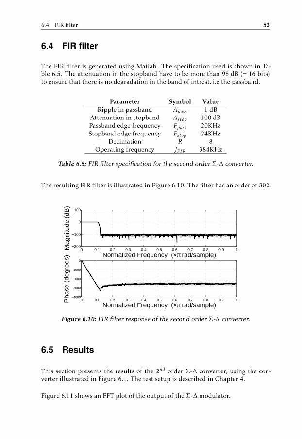
6.4 FIR filter
The FIR filter is generated using Matlab. The specification used is shown in Ta-ble 6.5. The attenuation in the stopband have to be more than 98 dB (= 16 bits)to ensure that there is no degradation in the band of intrest, i.e the passband.
Parameter Symbol ValueRipple in passband Apass 1 dB
Attenuation in stopband Astop 100 dBPassband edge frequency Fpass 20KHzStopband edge frequency Fstop 24KHz
Decimation R 8Operating frequency fFIR 384KHz
Table 6.5: FIR filter specification for the second order Σ-∆ converter.
The resulting FIR filter is illustrated in Figure 6.10. The filter has an order of 302.
0 0.1 0.2 0.3 0.4 0.5 0.6 0.7 0.8 0.9 1−4000
−3000
−2000
−1000
0
Normalized Frequency (×π rad/sample)
Pha
se (
degr
ees)
0 0.1 0.2 0.3 0.4 0.5 0.6 0.7 0.8 0.9 1−200
−100
0
100
Normalized Frequency (×π rad/sample)
Mag
nitu
de (
dB)
Figure 6.10: FIR filter response of the second order Σ-∆ converter.
6.5 Results
This section presents the results of the 2nd order Σ-∆ converter, using the con-verter illustrated in Figure 6.1. The test setup is described in Chapter 4.
Figure 6.11 shows an FFT plot of the output of the Σ-∆ modulator.

54 6 Implementation of a Second Order Σ-∆ Converter
0 0.1 0.2 0.3 0.4 0.5−160
−140
−120
−100
−80
−60
−40
−20
0
Frequency [ f / fs ]
PS
D [
dB
]SNR = 80.3dB SNDR = 80.3dB THD = −104.3dB SFDR = 104.8dB ENOB = 13.04bits
H2 = −107.0dBFS
H3 = −123.7dBFSH
4 = −123.6dBFSH
5 = −122.0dBFS H
6 = −125.3dBFSH
7 = −125.5dBFS
H8 = −130.4dBFS
H9 = −125.4dBFS H
10 = −128.8dBFS
H1 = −2.1dBFS
Figure 6.11: FFT plot of an input frequency of 10KHz -3dBFS using 65536points FFT.
Figure 6.12 shows the SNDR/SNR vs. input frequency of the output of the Σ-∆modulator.
0 0.05 0.1 0.15 0.2 0.25 0.3 0.35 0.4 0.45 0.570
75
80
85
Relative Frequency f/fOUT
SN
R/S
ND
R [d
B]
SNRSNDR
Figure 6.12: SNR and SNDR vs. frequency using an -3dBFS input signal.

6.5 Results 55
Figure 6.13 shows the SNDR/SNR vs. input amplitude of the output of the Σ-∆modulator.
−80 −70 −60 −50 −40 −30 −20 −10 00
10
20
30
40
50
60
70
80
Input Amplitude
SN
R/S
ND
R [d
B]
SNRSNDR
Figure 6.13: SNR and SNDR vs. input amplitude, using a 7.3KHz inputfrequency.
6.5.1 FPGA resources
Table 6.6 shows the FPGA resources used. The "other" row includes e.g. a S/PDIFdriver and the sampling register. Three pins on the FPGA are used for the secondorder active loop-filter Σ-∆ converter.
Slice Regs LUTs Block RAM DSP DCM/PLLFIR 305 200 3 3 0CIC 209 122 0 2 0
Other 97 108 0 0 1Total 611 430 3 5 1
FPGA utilization 5% 7% 4% 31% 50%
Table 6.6: FPGA resources used in the second order Σ-∆ Converter.

56 6 Implementation of a Second Order Σ-∆ Converter
6.6 Discussion
The results in Section 6.5 will be discussed here.
According to Figure 6.11 and Figure 6.13 the peak SNDR is about 80.3dB for thesecond order Σ-∆ converter, i.e.:
SNDRpeak = 10log10
S2
E2n,d + E2
in,n,d
= 80.3dB, (ENOB = 13.04 bits). (6.9)
Where S is the input signal power, En,d is the noise and the distortion power gener-ated in the converter. Ein,n,d is noise and distortion in the input signal. Accordingto Figure 4.2 and Figure 4.4, the peak SNDR for the M-audio test equipment isabout 86.1 dB. Therefore the input signal has an SNDR of:
SNDRin,peak = 10log10
S2
E2in,n,d
= 86.1dB, (ENOB = 14.01 bits). (6.10)
The second order Σ-∆ modulator is about 6dB (equivalent to about 1 bit) worsethan the input signal. The ideal SNDR peak is, by combining Equation 6.9 andEquation 6.10:
SNDRin,peak = 10log10
S2
E2n,d
= 81.6dB, (ENOB = 13.26 bits). (6.11)
According to Equation 6.11, the dominant noise and distortion comes from themodulator itself. The simulation result in Section 6.2.2, claims a theoreticalENOB of above 16 bits. The additional noise and distortion may come from clockjitter, ELD, ISI, power supply noise, cuircuit noise and operational amplifier non-idealities inter alia, as discussed in Section 3.3. Further investigation has to bedone to find the dominant noise/distortion source to further improve the con-verter.
Table 6.6 in Section 6.5.1, the used resources for the second order Σ-∆ converteris listed. One can see that the FIR filter and the CIC filter are occupying the most"area" in the FPGA. This area can be optimized by, e.g., changing the specificationand parameters of the filters.
7Conclusions and Future Work
Conclusions and future work will be presented in this chapter.
7.1 Conclusions
Table 7.1 shows a comparison between the passive Σ-∆ converter (from Chap-ter 5), the second order Σ-∆ converter (from Chapter 6) and the converter thatis used today in a product from Actiwave: PCM1807 from Texas Instruments. Ihave used the same test setup as in Figure 4.1 to test the PCM1807, except that itis powered from another power supply.
Since the PCM1807 is a dual channel ADC, the resources are divided by two inorder to compare it with my two solutions. The prices of PCM1807 ($0.90) andLMV793 ($0.45) are taken from Texas Instruments website [9][7]. The price forthe passive components (resistors and capacitors) are set to $0.01. The pricesdon’t include the decoupling capacitors needed.
With proper deisgn and careful PCB layout with the PCM1807, the theoreticalSNDR is typical 93dB (ENOB ∼15.15) according to the datasheet of the PCM1807[21]. But in order to compare the A/D converters, the same test setup is used(except for another power supply used for PCM1807).
According to Table 7.1, there can be conclusions:
1. The first order passive CT Σ-∆ is moderate in SNDR, but with low cost ofexternal components and with relative large FPGA area. If there’s a priorityin low-cost the first order passive CT Σ-∆ is a good choice.
2. The second order CT Σ-∆ have the best SNDR, but with large FPGA area
57

58 7 Conclusions and Future Work
1st order passive 2nd order Actiwave ABDynamic parameter CT Σ-∆ CT Σ-∆ with TI PCM1807
SNRpeak [dB] 63 80.3 77.9SNDRpeak [dB] 62.3 80.3 77.8ENOBpeak [bits] 10.06 13.04 12.63
Resources/channelFPGA
# I/O pins 3 3 4/2# Slice regs 599 611 256/2
# LUTs 408 430 146/2# Block RAMs 5 3 0/2
# DSP 8 5 0/2# DCM/PLL 1 1 1/2
Resources/channelComponents
# Active components 0 1 1/2# Passive components 6 8 2/2
Total price [$] 0.06 0.53 0.46
Table 7.1: Comparison between the A/D converters. Since the PCM1807 isa dual channel ADC, its resources are divided by two.
and highest cost per channel. With demands for good quality in SNDR thesecond order CT Σ-∆ is a good choice.
3. The PCM1807 have good SNDR, small FPGA area and fairly high cost of ex-ternal components. If there’s demand for small FPGA area and good qualityin SNDR an external ADC (such as the PCM1807) is a good choice.
There seems to be a tradeoff between quality (e.g. SNDR), FPGA area and cost.
It is some difficulty to compare the two converters presented in this thesis withthe PCM1807. For instance, PCM1807 need two voltages (3.3V and 5V) in orderto function [21]. This add up to the total price for the Actiwave AB solution,which is not listed in Table 7.1.
The two converters presented in this thesis can easily be doubled in order to con-vert stereo audio (like the PCM1807). This doesn’t necessary scale the resourcesof the FPGA and the total price by a factor of two. For instance, one can useLMV794 (which is two LMV793 in a single package) for the second order CT Σ-∆ converter in order to convert stereo audio. The price for LMV794 is $0.63 [8]which implies a total price of $0.71 for the second order CT Σ-∆ converter withdual channel. The corresponding total price for the PCM1807 (dual channel) is$0.92.
The two converters presented in this thesis can be used for other purposes. Forexample, the passive Σ-∆ converter can easily be modified to be able to convertother analog signals, e.g. signals from sensors that perhaps only need 10 bits

7.2 Future Work 59
ENOB and is very low-cost.
The recommendation for Actiwave AB is not to use the passive CT Σ-∆ converterfor audio applications. Since Actiwave AB is working with high precision audio,this is not an option. But the passive CT Σ-∆ converter can be used for otherapplications, e.g. convert analog signals from sensors.
To cut cost, Actiwave AB could use the second order Σ-∆ converter in a dualchannel configuration (with LMV794) instead of the PCM1807. However, theLVM794 has to be tested and further investigation of the second order CT Σ-∆converter is necessary in order to achieve 16 bits ENOB.
7.2 Future Work
The things that can be done in the future are listed below:
• More testing has to be done in order to further characterize both the passiveand the active Σ-∆ converter. The input (test) signal needs to have betterquality than the converter itself.
• The digital filters in the FPGA can be further optimized. The FIR filtersare quite long (order of 603 and 302 for the passive and the active Σ-∆,respectively) and take up relative large FPGA area.
• For the passive Σ-∆ converter there can be more investigation on the pas-sive filter. Perhaps a higher order filter or a RLC-filter can achieve betterresolution.
• Further investigation on the DAC pulse shape can be done. There are sev-eral types of pulse shapes that are not rectangular (NRZ, RZ, HRZ) such ase.g. SCR (Switched-Capacitor-Resistor). Perhaps one can take advantage ofthe parasitic capacitance assosiated with the pad (described in Section 5.2)to implement a SCR DAC pulse.
• A differential solution for the second order active Σ-∆ converter, can possi-ble be more immune to noise and non-idealities.
• Further investigation on what the dominant noise source can be done inorder to achieve better quality on the converters.

60 7 Conclusions and Future Work

List of Figures
2.1 The complete system. . . . . . . . . . . . . . . . . . . . . . . . . . . 52.2 Simplified LVDS schematic [18]. . . . . . . . . . . . . . . . . . . . . 62.3 Hysteresis of a comparator [1]. . . . . . . . . . . . . . . . . . . . . . 72.4 Different ADC architectures and applications [11]. . . . . . . . . . 8
3.1 From analog input signal, x(t), to output, y[n], which is later pro-cessed by e.g. a DSP [23]. . . . . . . . . . . . . . . . . . . . . . . . . 9
3.2 The sampling process. . . . . . . . . . . . . . . . . . . . . . . . . . . 103.3 xp in the frequency domain [5]. . . . . . . . . . . . . . . . . . . . . 113.4 Illustration of quantization. . . . . . . . . . . . . . . . . . . . . . . 123.5 Illustration of SFDR. . . . . . . . . . . . . . . . . . . . . . . . . . . 133.6 Spectral proporties for Nyquist-rate and oversampling ADC [10]. . 143.7 A first order Σ-∆ discrete time modulator. . . . . . . . . . . . . . . 153.8 Output waveform of a Σ-∆ converter with 1-bit quantizer (ADC). . 153.9 A linearization of a first order Σ-∆ discrete time modulator in the
z-domain. . . . . . . . . . . . . . . . . . . . . . . . . . . . . . . . . . 163.10 Noise PSD for Nyquist-rate, oversampling and oversampling+noise-
shaping (Σ-∆) ADC’s [10]. . . . . . . . . . . . . . . . . . . . . . . . 173.11 Maximum SQNR for different Σ-∆ orders and OSR with a 1-bit
quantizer . . . . . . . . . . . . . . . . . . . . . . . . . . . . . . . . . 183.12 Continuous-time Σ-∆ modulator. . . . . . . . . . . . . . . . . . . . 183.13 Open loop of DT and CT Σ-∆ [10]. . . . . . . . . . . . . . . . . . . 193.14 HDAC impulse response for NRZ, RZ and HRZ. . . . . . . . . . . . 193.15 A 2nd order DT Σ-∆ modulator in a feedback topology [10]. . . . . 203.16 A 2nd order CT Σ-∆ modulator. . . . . . . . . . . . . . . . . . . . . 203.17 A modified 2nd order CT Σ-∆ converter. . . . . . . . . . . . . . . . 213.18 A 2nd order CT Σ-∆ STF. . . . . . . . . . . . . . . . . . . . . . . . . 223.19 Noise sources
(E1(s), EQn(s)andEDAC(s)
)in a 1st order CT Σ-∆ mod-
ulator [5]. . . . . . . . . . . . . . . . . . . . . . . . . . . . . . . . . . 223.20 Output of a NRZ DAC suffering from excess loop delay, with time
delay td . . . . . . . . . . . . . . . . . . . . . . . . . . . . . . . . . . . 233.21 Illustration of a jittered clock, where the shadows represents the
clock uncertainty area. . . . . . . . . . . . . . . . . . . . . . . . . . 243.22 The RC-integrator [24]. . . . . . . . . . . . . . . . . . . . . . . . . . 24
61
62 LIST OF FIGURES
3.23 Magnitude response of an ideal NTF and NTF with an Op-ampwith finite DC gain (100K or 100 dB). . . . . . . . . . . . . . . . . . 25
3.24 NTF for different GBW. . . . . . . . . . . . . . . . . . . . . . . . . . 263.25 Low-pass filtering and decimation by a factor R. . . . . . . . . . . . 263.26 Illustration of a CIC filter. . . . . . . . . . . . . . . . . . . . . . . . 273.27 Magnitude respons for different filter order vs. frequency relative
to the low (decimated) sampling frequency, where R = 256 and M= 1. fB is 1/8 relative to the low sampling frequency. . . . . . . . . 28
3.28 CIC filter decimation by a factor R1 and conventional decimationfilter by a factor R2, where R = R1 × R2. . . . . . . . . . . . . . . . 28
4.1 Test setup for testing the converter. . . . . . . . . . . . . . . . . . . 294.2 65536 point FFT of the output of the M-Audio Fast Track Pro, us-
ing a -1dBFS and ∼7.3KHz input signal. The SNDR is verified (86dB), but the SNR is much lower than the stated 103 dB. . . . . . . 30
4.3 SNR/SNDR vs. frequency of M-Audio Fast Track Pro, using a -6dBFS input signal. . . . . . . . . . . . . . . . . . . . . . . . . . . . 30
4.4 SNR/SNDR vs. input amplitude of M-Audio Fast Track Pro, usinga ∼7.3KHz input signal. The claimed 86 dB SNDR is reached, butnot the claimed 103 dB SNR. . . . . . . . . . . . . . . . . . . . . . . 31
5.1 System overview of the passive Σ-∆ ADC. . . . . . . . . . . . . . . 335.2 Linearization of the passive Σ-∆ ADC. . . . . . . . . . . . . . . . . 345.3 NTF with passive loop-filter with different wp compared with an
active loop-filter. . . . . . . . . . . . . . . . . . . . . . . . . . . . . . 355.4 The passive Σ-∆ converter. . . . . . . . . . . . . . . . . . . . . . . . 355.5 Simple illustration of an 1-bit DAC. . . . . . . . . . . . . . . . . . . 365.6 Realization of the passive Σ-∆ converter [13]. . . . . . . . . . . . . 375.7 1024 point FFT plot of the output of the passive Σ-∆ modualtor.
The input signal is 2KHz and has an amplitude of 1V. . . . . . . . 375.8 SNDR and SNR vs. Input Frequency. Using a 1V input signal. . . . 385.9 Hysteresis effect of the comparator in the passive Σ-∆ modulator
with "ideal" filtering and decimation. Using 1024 point FFT, withHanning window and ∼2KHz input signal with amplitude of 1V. 38
5.10 SNDR vs. Hysteresis. Using a 1V input signal of 2KHz. . . . . . . 395.11 CIC filter response for the passive Σ-∆ converter. . . . . . . . . . . 405.12 FIR filter response for the passive Σ-∆ converter. . . . . . . . . . . 415.13 65536 point FFT plot of a 10 KHz -3dBFS input signal. . . . . . . . 415.14 SNR and SNDR vs. Frequency using a -3dBFS input signal. . . . . 425.15 SNR and SNDR vs. input amplitude using a 7.3KHz input signal. . 42
6.1 System overview of the second order Σ-∆ converter. . . . . . . . . 456.2 A 2nd order CT Σ-∆ feed-forward modulator. . . . . . . . . . . . . 466.3 Matlab simulation of the input to the quantizer with a1 = 1.5 and
k1 = 1. . . . . . . . . . . . . . . . . . . . . . . . . . . . . . . . . . . . 47

LIST OF FIGURES 63
6.4 Matlab simulation of the input to the quantizer with a1 = 2.5 andk1 = 156. . . . . . . . . . . . . . . . . . . . . . . . . . . . . . . . . . 47
6.5 Realization of the 2nd order CT Σ-∆ modulator. . . . . . . . . . . . 486.6 Simulation of the SR in the Op-amp in the second order Σ-∆ mod-
ulator. . . . . . . . . . . . . . . . . . . . . . . . . . . . . . . . . . . . 496.7 Simulation result of the second order Σ-∆ modulator using 1024
points FFT, 1V input amplitude (-4.3 dBFS). . . . . . . . . . . . . . 506.8 Simulation result of the second order Σ-∆ modulator, SNR/SNDR
vs. Frequency. . . . . . . . . . . . . . . . . . . . . . . . . . . . . . . 516.9 CIC filter response of the second order Σ-∆ converter. . . . . . . . 526.10 FIR filter response of the second order Σ-∆ converter. . . . . . . . 536.11 FFT plot of an input frequency of 10KHz -3dBFS using 65536
points FFT. . . . . . . . . . . . . . . . . . . . . . . . . . . . . . . . . 546.12 SNR and SNDR vs. frequency using an -3dBFS input signal. . . . . 546.13 SNR and SNDR vs. input amplitude, using a 7.3KHz input fre-
quency. . . . . . . . . . . . . . . . . . . . . . . . . . . . . . . . . . . 55

List of Tables
1.1 The outline of the thesis. . . . . . . . . . . . . . . . . . . . . . . . . 3
2.1 Xilinx Spartan-6 XC6LX9 FPGA Features (TQG144 package). . . . 62.2 LVDS I/O Standard Input Levels Xilinx Spartan-6. . . . . . . . . . 72.3 Analog audio input signal specification. . . . . . . . . . . . . . . . 7
3.1 α and β values for NRZ, RZ and HRZ DAC’s. . . . . . . . . . . . . 19
5.1 Specification for the passive Σ-∆ ADC. . . . . . . . . . . . . . . . . 345.2 Component values for the passive Σ-∆ modulator. . . . . . . . . . 365.3 Parameters of the CIC filter for the passive Σ-∆ converter. . . . . . 395.4 FIR filter specification for the passive Σ-∆ converter. . . . . . . . . 405.5 FPGA resources used in the passive first order Σ-∆ Converter. . . . 43
6.1 Specification for the second order Σ-∆ ADC. . . . . . . . . . . . . . 466.2 Component values for the loop filter in the second order Σ-∆ mod-
ulator. . . . . . . . . . . . . . . . . . . . . . . . . . . . . . . . . . . . 496.3 OP-amp specifications. . . . . . . . . . . . . . . . . . . . . . . . . . 506.4 CIC filter parameters for the second order Σ-∆ converter. . . . . . 526.5 FIR filter specification for the second order Σ-∆ converter. . . . . . 536.6 FPGA resources used in the second order Σ-∆ Converter. . . . . . 55
7.1 Comparison between the A/D converters. Since the PCM1807 is adual channel ADC, its resources are divided by two. . . . . . . . . 58
64
Bibliography
[1] Analog Devices. Comparators, September 2011. MT-083, Rev. A. Cited onpages 7 and 61.
[2] Pervez M. Aziz, Henrik V. Sorensen, and Jan Van Der Spiegel. An Overviewof Sigma-Delta Converters: How a 1-bit ADC achieves more than 16-bitresolution. IEEE Signal Processing Magazine, 13:61, 1996. Cited on pages10 and 11.
[3] Feng Chen and Bosco Leung. A 0.25-mW Low-Pass Passive Sigma-DeltaModulator with Built-In Mixer for a 10-MHz IF Input. IEEE Journal of Solid-State Circuits, 32(6):774–782, 1997. Cited on pages 34 and 35.
[4] Matthew P. Donadio. CIC Filter Introduction. July 2000. Cited on page 26.
[5] Julian M. Garcia. Digitally Enhanced Continuous-Time Sigma-DeltaAnalogue-to-Digital Converters. PhD thesis, KTH Royal Institute of Tech-nology, 2012. ISBN: 978-91-7501-360-2. Cited on pages 10, 11, 12, 13, 18,22, 23, and 61.
[6] Eugene B. Hogenauer. An Economical Class of Digital Filters for Decima-tion and Interpolation. IEEE Transactions on Acoustics, Speech, and SignalProcessing, ASSP-29, No. 2, April 1981. Cited on pages 27 and 28.
[7] Texas Instruments. LMV793, July 9 2013.http://www.ti.com/product/lmv793. Cited on page 57.
[8] Texas Instruments. LMV794, July 9 2013.http://www.ti.com/product/lmv794. Cited on page 58.
[9] Texas Instruments. PCM1807, July 9 2013.http://www.ti.com/product/pcm1807. Cited on page 57.
[10] Zhang Jinghua. Low-Voltage Low-Power Continuous-Time Delta-SigmaModulator Designs. PhD thesis, National University of Singapore, 2010.Cited on pages 8, 13, 14, 15, 17, 18, 19, 20, 23, 24, 25, and 61.
65

66 Bibliography
[11] Walt Kester. Which ADC Architecture Is Right for Your Application? Ana-log Dialogue, (39), June 2005. Cited on pages 8 and 61.
[12] Scott D. Kulchycki. Continuous-Time Sigma-Delta ADCs. ADC12EU050,January 2008. Cited on page 17.
[13] Lattice Semiconductor Corporation. Simple Sigma-Delta ADC, November2010. RD1066. Cited on pages 2, 37, and 62.
[14] M-Audio/ Avid Technology, Inc. Fast Track Pro User Guide, 2010. GuidePart Number 9329-65014-00 REV A 05/10. Cited on pages 29 and 30.
[15] M. Ortmanns and F. Gerfers. Continuous-Time Sigma-Delta A/D Conver-sion. Springer, 2006. ISBN 10-3-540-28406-0. Cited on pages 23, 24, 25,and 26.
[16] Matthew Jeremiah Park. A 4th Order Continuous-Time Σ-∆ ADC with VCO-Based Integrator and Quantizer. PhD thesis. Cited on page 24.
[17] Pavel Peev, Bart De Vuyst, Pieter Rombouts, and Anas A. Hamoui. An Anti-Aliasing Filter inspired by Continuous-Time Σ-∆ Modulation. Cited on page21.
[18] Fabio Sousa, Volker Mauer, Neimar Duarte, Ricardo P. Jasinski, and Volnei A.Pedroni. Taking Advantage of LVDS Inpus Buffers To Implement Sigma-Delta A/D Converters in FPGAs. IEEE International Symposium on Circuitsand Systems, 1, 2004. Cited on pages 6 and 61.
[19] Fabio Sousa, Volker Mauer, Neimar Duarte, Ricardo P. Jasinski, and Volnei A.Pedroni. Taking Advantage of LVDS Input Buffers to Implement Sigma-Delta A/D Converters in FPGAs. Circuits and Systems, 2004. ISCAS ’04.Proceedings of the 2004 International Symposium on, 1:1088–1091, 2004.ISBN: 0-7803-8251-X. Cited on pages 2 and 7.
[20] Texas Instruments. LVDS Owner’s Manual Including High-Speed CML andSignal Conditioning, Fourth edition. Cited on page 6.
[21] Texas Instruments. PCM1807: Single-Ended, Analog-Input 24-Bit, 96-kHzStereo A/D Converter, September 2005. SLES147. Cited on pages 1, 57,and 58.
[22] Texas Instruments. LMV793/LMV794 88 MHz, Low Noise, 1.8V CMOSInput, Decompensated Operational Amplifiers, 2007. Cited on page 50.
[23] Lars Wanhammar. DSP Integrated Circuits. Academic Press, 1999. ISBN0-12-734530-2. Cited on pages 9 and 61.
[24] Lars Wanhammar. Analog Filters Using MATLAB. Springer, 2009. ISBN978-0-387-92766-4. Cited on pages 24, 48, and 61.
[25] Xilinx. Spartan-6 Family Overview, v.2.0 edition, October 2011. DS160.Cited on page 6.

Bibliography 67
[26] Xilinx. Spartan-6 FPGA Data Sheet: DC and Switching Characteristics, v.3.0edition, October 2011. DS162. Cited on pages 6 and 36.
[27] Axel Zimmermann, Endric Schubert, and Christian Grumbein. Integrationof Analog-Digital and Digital-Analog Converters into FPGA-Based Micro-controllers. 2011. Cited on page 2.

68 Bibliography
Upphovsrätt
Detta dokument hålls tillgängligt på Internet — eller dess framtida ersättare —under 25 år från publiceringsdatum under förutsättning att inga extraordinäraomständigheter uppstår.
Tillgång till dokumentet innebär tillstånd för var och en att läsa, ladda ner,skriva ut enstaka kopior för enskilt bruk och att använda det oförändrat för icke-kommersiell forskning och för undervisning. Överföring av upphovsrätten viden senare tidpunkt kan inte upphäva detta tillstånd. All annan användning avdokumentet kräver upphovsmannens medgivande. För att garantera äktheten,säkerheten och tillgängligheten finns det lösningar av teknisk och administrativart.
Upphovsmannens ideella rätt innefattar rätt att bli nämnd som upphovsmani den omfattning som god sed kräver vid användning av dokumentet på ovanbeskrivna sätt samt skydd mot att dokumentet ändras eller presenteras i sådanform eller i sådant sammanhang som är kränkande för upphovsmannens litteräraeller konstnärliga anseende eller egenart.
För ytterligare information om Linköping University Electronic Press se förla-gets hemsida http://www.ep.liu.se/
Copyright
The publishers will keep this document online on the Internet — or its possi-ble replacement — for a period of 25 years from the date of publication barringexceptional circumstances.
The online availability of the document implies a permanent permission foranyone to read, to download, to print out single copies for his/her own use andto use it unchanged for any non-commercial research and educational purpose.Subsequent transfers of copyright cannot revoke this permission. All other usesof the document are conditional on the consent of the copyright owner. Thepublisher has taken technical and administrative measures to assure authenticity,security and accessibility.
According to intellectual property law the author has the right to be men-tioned when his/her work is accessed as described above and to be protectedagainst infringement.
For additional information about the Linköping University Electronic Pressand its procedures for publication and for assurance of document integrity, pleaserefer to its www home page: http://www.ep.liu.se/
© Johan Hellman