control algorithm based on limit cycle oscillator-fll for
TRANSCRIPT

This article has been accepted for publication in a future issue of this journal, but has not been fully edited. Content may change prior to final publication.
1
1
Abstract-The present paper involves a Limit Cycle
Oscillator-Frequency Lock Loop (LCO-FLL) based control
algorithm for unified power quality controllers-S type (UPQC-S)
towards compensation of reactive power, to maintain unity power
factor, regulate constant voltage at PCC, mitigate sag, swell and
to eliminate harmonics. In this approach, an extraction of
fundamental in-phase and quadrature components for the
estimation of reference signals are taken from LCO-FLL circuit.
The control LCO-FLL provides a high grade of protection against
sag-swell voltages, unbalance loading and harmonics present in
the utility grid. In addition to that, it has advantageous
characteristic of synchronization with the grid frequency at any
aforesaid conditions without use of phase locked loop or
trigonometric functions. Other advantages of the LCO-FLL are to
give useful information to estimate fundamental components from
a highly polluted grid scenario. The values obtained from JAYA
optimization algorithm is used to fine-tune proportional integral
(PI) controller gains, so that it maintained DC link voltage to
desired level. The mean square error (MSE) is employed as an
objective function for optimizing the error between actual and
reference value. The control algorithm based on LCO-FLL is
developed in MATLAB/Simulink software and it is tested for
power conditioning features.
Keywords―LCO-FLL, JAYA, PI-Tuning, MSE, Sag,
unbalanced, VSC.
I. INTRODUCTION
ODERN power systems are design to operate
efficiently to supply power on demand to various load
centres with high reliability [1]. Moreover, it is degraded
due to sudden rise of power electronics based appliances at
household and industrial sectors. In [2], these non-linear
devices inject non sinusoidal current and degrade efficiency,
power factor, overheating of devices and so on that is leads to
deterioration of power quality (PQ) in the distribution system.
Apart from that [3], the degree of waveform distortion is
increasingly serious now; such effects have brought the PQ
issue as an increasing concern in the power systems network.
Compensating type custom power devices are one of effective
solution to solve power quality issues in distribution network
[4].
Manuscript received 02- February 2019, revised 17-May-2019, revised
21-August 2019, accepted 17- February 2020.
Sabha Raj Arya and Sayed Javed Alam are Department of Electrical Engineering, Sardar Vallabhai National Institute of Technology, Suart-395007,
India
(E-mail: [email protected] and [email protected]) Papia Ray is with Department of Electrical Engineering, Veer Surendra Sai
University of Technology, Burla, Sambalpur, India (email: [email protected])
DOI: 10.17775/CSEEJPES.2019.01030
These devices are classified in three categories such as shunt,
series and combination of shunt-series types. Generally, all of
them use voltage source converters (VSC) which is controlled
by various control strategies. If the device is connected shunt
then it is known as distribution static compensator
(DSTATCOM) [5], whereas series connected active filter is
carried out for voltage compensation commonly known as
Dynamic Voltage Restorer (DVR) [6]. However, these
individual compensation techniques are insufficient to solve
distribution side power quality difficulties concurrently for
current and voltage. So, in [7] the author proposed an active
power line conditioner (APLC) which mitigates current and
voltage compensation simultaneously with combined use of
shunt and series devices. The combination of shunt and series
devices is referred as unified power quality controllers (UPQC)
is used in power distribution system for compensation of
current and voltage based power quality problems [8]. UPQC is
classified based on rating calculation with respect to voltage
injection method [9]. Considering literature survey on voltage
injection techniques, the UPQC-S is found better among other
UPQC topologies [10].The UPQC-S shows several advantages
over conventional UPQC. The UPQC-S not only compensates
reactive power but it also reduces size of both voltage source
converter (VSC) rating, shares reactive power between both
VSCs and effectively use of series injection transformers
etc[11]. A brief comparison is given in table-1 based on
injection voltage control approaches which shows selected
UPQC-S has more advantages over conventional UPQC.
TABLE 1. COMPARISON BETWEEN DIFFERENT UPQC.
Sr.
No.
Type of
UPQC
Comparison in terms of features and limitations
1. UPQC-P [12]
(a) It is in-phase voltage control approach. (b) It provides active power compensation in which
series voltage is injected in phase with current
through series VSC. (c) The voltage sag and swell is mitigated by injecting
active power through series injection transformer.
(d) “P” is referred as active power control. (e) To compensate sag and swell; it required smaller
magnitude of voltage from series injection
transformer. (i.e. it requires the minimum series injection voltage.)
2. UPQC-Q
[13]
(a) It is an in-quadrature voltage control approach.
(b) It provides reactive power compensation in which
series voltage is injected in-quadrature with current through series VSC.
(c) The voltage sag is mitigated by injecting reactive
power through series injection transformer. (d) “Q” is referred as reactive power control.
(e) To compensate sag; it required larger magnitude of voltage from series injection transformer. (i.e. it
Control Algorithm based on Limit Cycle
Oscillator-FLL for UPQC-S with Optimized PI
Gains Sabha Raj Arya, Senior Member, IEEE, Sayed Javed Alam and Papia Ray, Senior Member, IEEE
M

This article has been accepted for publication in a future issue of this journal, but has not been fully edited. Content may change prior to final publication.
2
2
requires a maximum series injection voltage and it
will not compensate swell)
3 Minimum VA Loading
[14]
(a) It is an injection of voltage at a certain angle with minimum VA loading approach.
(b) It provides reactive as well as active power
compensation in which a series voltage is injected at a certain minimum angle with current through series
VSC.
(c) The series voltage injection and current drawn by shunt VSC must need for determining minimum VA
loading.
4 UPQC-S [10]
(a) The series voltage is injected at a certain minimum angle with respect to the source current
through series VSC.
(b) It provides sag and swells compensation and sharing reactive power with both VSC.
(c) “S” is stand because of delivering active and
reactive power control. (d) Besides the series voltage injection by series VSC,
the overall power balance and dc voltage is
maintained by the current drawn through the shunt VSC.
Based on the control algorithms, the response of the UPQC is
governed by the DSTATCOM and DVR. In [15],
proportional-resonant controller and a resonant controller are
used to mitigate voltage based power quality problem. Another
side, proportional-integral (PI) controller and three vector PI
controller is used for mitigation of current based power quality
problems. These controllers are developed based on controller
gain parameters precisely with system parameters. In [16], the
synchronous reference frame control operation has been
developed to improve the performance analysis of single phase
UPQC, to compensate PQ issues in conventional power
distribution system. An unit vector based control [17] is tested
to control VSC based series and shunt filter used as single phase
UPQC. The drawback of these controller are required an
adequate amount of knowledge of prior PQ issues in the
computation method and more sensitive with respect to out of
error regulator output signal. The classical control on UPQC is
IRPT based control i.e. based on p-q calculation [18],
synchronous reference frame theory [19], unit vector template
generation theory [20] and others. These controls are very
much sensitive with cut off frequency of used low pass filter,
tuning of PI controller gain and non-idealist of utility. So, zero
crossing detection (ZCD) merged with the Low Pass Filter
(LPF) [21] and Phase Lock Loop (PLL) [22] are incorporates
with these control algorithm to identify the phase of the system
voltage. Authors in [23] discussed the more advanced and
characteristics performance of different PLLs. This PLL are
accountable for control and synchronization of grid attached
VSC [24]. The PLLs based algorithms can successfully reject
above mentioned PQ perturbations and simultaneously, it
provide the magnitude, phase, frequency and time varying
fundamental parameters of the distorted grid supply. Due to
these characteristics, aforesaid [22-24] PLLs are used in
compensating devices for mitigation of all power quality
perturbations. In literature [25], Limit Cycle Oscillator (LCO)
is proposed by authors with Frequency Lock Loop (FLL) [26]
which make the system frequency adaptive coupled with limit
cycles theory [27]. This LCO-FLL is capable of generating
synchronized signals with constant amplitude. It also rejects
harmonics and handled frequency shift variations in phase
during highly distorted grid. Due to the non-linearity structure
of LCO-FLL system, it is robust against above foresaid
perturbations. So, in this work a proposal has been made with
the application of LCO-FLL in the control algorithm of
UPQC-S.
Along with control algorithm, the tuning of PI-controller gains
is one of the most essential works in such applications for
controlling the error signal of the internal control circuit. In
literature survey a numerous propose schemes are incorporated
for evaluating gains of PI-Controllers [28-30]. Such design
parameters value might not provide satisfactory results under
dynamic working conditions or when the system is highly
nonlinear complex structure. This is because of arithmetical
formulation is based on classical method, certain limitation on
design parameters and some initial assumptions. To overcome
this, a meta-heuristic optimization and evolutionary technique
has been proposed by the various researchers in distribution
side compensating devices [14,28, 30,32]. The performance of
nature inspired evolutionary optimization like PSO, GWO, GA,
etc are affected by their specific control variables values like
size of the population, number of particles generation, weight
of adjacent group etc. If the selection of these variables is not
proper then it may convergence to any local minimum or may
reduce the effectiveness of the system. Whereas, in [31] the
meta-heuristic optimization technique are free from specific
control parameters. The JAYA optimization has less number of
function evaluations and no difficulty in resolving discrete
optimization with less design variables [32]. It has tendency to
find best solution and avoid worst solution. Therefore, the
JAYA algorithm is useful for the calculations of PI gains to
achieve better performance to maintain power quality issue.
In this paper UPQC-S controller is designed using p-q theory
based on fundamental positive sequence detection through
LCO-FLL for the reference signal generation. The special
feature of LCO-FLL is that it is nearly global asymptotical
stable closed orbit in the phase plan and its convergence does
not depend on the preliminary circumstances. This LCO-FLL is
a frequency adaptive and provides time varying fundamental
parameters but the extraction of fundamental positive sequence
component (FPSC) is essential in construction of control
scheme for UPQC-S. Authors in the literature [33], proposed a
FPSCs extraction using method of symmetrical components for
power system. Furthermore, a manual (trial and error)
PI-Controller fine-tuning procedure will acquire significant
amount of time for its parametric value tuning [34]. Here, the
UPQC-S itself a complex system and its PI controller gains
calculation is tedious work. To overcome this, JAYA
optimization is taken for controller gains fine-tuning, as it is
straightforward and free from algorithm control parameters.
The specialty of this optimization is less complexity, less
computation time and faster convergence characteristics over
other nature inspired evolutionary optimization algorithms like
PSO, GWO, GA, etc. The numerical values obtained by JAYA
algorithm are selected as a PI-controller gains and it’s again
improves the UPQC-S controller performance. The simulink
model of UPQC-S with LCO-FLL control algorithm is
developed using MATLAB tools and its performance are
evaluated for a non linear load under aforesaid PQ
perturbations.
This article has been accepted for publication in a future issue of this journal, but has not been fully edited. Content may change prior to final publication.
3
3
II. DESCRIPTION OF UPQC
The illustrative diagram of a UPQC connected to a three phase
ac grid with source impedance (Zs) is shown in Fig.1. A ripple
filter (Cf, Rf) installed at appropriate places as depicted in Fig.1
to eliminate high frequency switching noise. One VSC acting
as a shunt and it work as current controlled source connected
through interfacing inductor (Lsh) to the main line. The other as
series VSC act as a voltage controlled source connected
through series transformer. Each VSC is designed using six
Insulated Gate Bipolar Transistor (IGBT) switches. The DC
link voltage (Vdc) is controlled by these VSC through the
proposed LCO-FLL based control algorithm along with
PI-Controller and SPWM switching technique. To analysis the
performance of UPQC as UPQC-S configuration, the non linear
bridge rectifier is considered as consumer load. The values of
the power and control circuit parameters and the load under
considerations for simulation work is specified in Appendix.
Fig. 1.UPQC block diagram
III. DETAILS OF CONTROL ALGORITHM
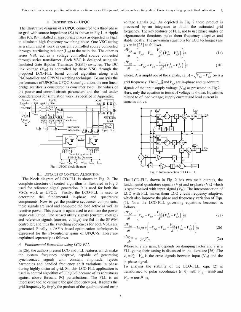
The block diagram of LCO-FLL is shown in Fig. 2. The
complete structure of control algorithm is illustrated in Fig 3
used for reference signal generation. It is used for both the
VSCs work as UPQC. Firstly, the LCO-FLL is used to
determine the fundamental in-phase and quadrature
components. Now to get the positive sequences components,
these signals are used and computed the load active as well as
reactive power. This power is again used to estimate the power
angle calculation. The sensed utility signals (current, voltage)
and reference signals (current, voltage) are fed to the SPWM
controller, and thus the switching sequences for both VSCs are
generated. Finally, a JAYA based optimization techniques is
expressed for the PI-controller gains of UPQC-S. These are
explained separately as follows.
A. Fundamental Extraction using LCO-FLL
In [26], the authors present LCO and FLL features which make
the system frequency adaptive, capable of generating
synchronized signals with constant amplitude, rejects
harmonics and handled frequency shift variations in phase
during highly distorted grid. So, this LCO-FLL application is
used in control algorithm of UPQC-S because of its robustness
against above foresaid PQ perturbations. The FLL is an
impressive tool to estimate the grid frequency (ω). It adapts the
grid frequency by imply the product of the quadrature and error
voltage signals (ev). As depicted in Fig. 2 these product is
processed by an integrator to obtain the estimated grid
frequency. The key features of FLL, not to use phase angles or
trigonometric functions make them frequency adaptive and
stable locally. The governing equations for LCO techniques are
given in [25] as follows.
2 2
2ω
f f
f f f f
dV VV V V V
dt A
(1a)
2 2
2ω
f f
f f f f
dV VV V V V
dt A
(1b)
where, A is amplitude of the signals, i.e. 2 2 f fA V V ;ω is a
grid frequency. The 牋fV and fV are in-phase and quadrature
signals of the input supply voltage (Vin) as presented in Fig.2.
Here, only the equation in terms of voltage is shown. Equations
related to of load voltage, supply current and load current is
same as above.
Fig. 2. Interconnection of LCO-FLL
The LCO-FLL shown in Fig. 2 has two main outputs, the
fundamental quadrature signals (Vfβ) and in-phase (Vfα) which
is synchronised with input signal (Vin). The interconnection of
LCO with FLL makes them LCO circuit frequency adaptive,
which also improve the phase and frequency variation of Eqn.
(1). Now the LCO-FLL governing equations becomes as
follows,
2 2
2ω
f f
f f f f
dV VV V V V
dt A
(2a)
2 2
2ω ω
f f
v f f f f
dV Vke V V V V
dt A
(2b)
FLLv f
de V
dt
(2c)
Where k, γ are gain; k depends on damping factor and γ is a
FLL gains; their tuning is discussed in the literature [26] .The
v in fe V V is the error signals between input (Vin) and the
in-phase signal.
To analysis the stability of the LCO-FLL, eqn. (2) is
transformed to polar coordinates (r, θ) with rsinfV and
rcosfV as,

This article has been accepted for publication in a future issue of this journal, but has not been fully edited. Content may change prior to final publication.
4
4
3
2sin θ ωv
dr rr ke
dt A
(3a)
θ ω
cos θr
v
dr ke
dt (3b)
γ rcos θv
de
dt
(3c)
In order to includes the dynamic perturbations in the input
signals, a phase error element is introduces as,
ref (4)
Now with these phase error variable, the dynamics of Eqn. (3)
illustrated as,
3
2sin ωv ref
dr rr ke
dt A
(5a)
ω
cosr
ref v ref
dr ke
dt
(5b)
γ rcosv ref
de
dt
(5c)
with v in refe V rsin . It is absorbed that the Eqn. (5)
has the equilibrium point at * ? { , 0, }in ref refx V Asin r A
The Jacobian of system matrix of the Eqn. (5) at equilibrium
point is given as,
2
* 2
2 2
2 sin cos 0
x cos cos 1
γ cos γ cos 0
ref ref ref ref ref
ref
ref ref ref ref
ref ref ref
k ksin
耴 sin kA
Asin A
(6)
According to Krasovskii Method [34] of constructing
Lyapunov Function for a non linear system is
* *x xTQ 翽 P?
(7)
where *x is Jacobian matrix of nonlinear system at
equilibrium points (x*) and P is a symmetrical positive definite
matrix and it is defined as,
11 12 13
21 21 21
31 31 31
P P P
P P P P
P P P
Since P is positive definite matrix according to Lyapunov
Function so, Q should also be a positive definite matrix which
is asymptotically stable at origin or equilibrium point. For the
system Eqn. (5a) to be asymptotically stable at the equilibrium
point x*, Q is positive definite matrix i.e.
2
21 112 2 sin cos 0ref
ref ref ref refPk ksin PA
(8)
3 3 2
13
2 2
12 21
22
(4 ...................0
( ) ( ) ) /
P A
ref
ref ref refP A cos ksin P A
P (9)
3 2 4
13
2 2 2 2
33 1
3 2
2
12 23..........( sin cos0
( ) ) /
....
ref ref ref
ref ref
AP k
sin P A k A
P P
P (10)
From these Eqn.(8-10) for all values of k and γ in the given
system is asymptotically stable at equilibrium point (x*).
The fundamental quadrature signals (Vfβ) and in-phase (Vfα)
which are obtained formed LCO-FLL is again used by UPQC-S
control for the generation of reference signals for both VSCs.
The complete reference signals generation for both VSCs is
depicted in Fig, (3) and explained below.
B. Reference Signal Generation for VSC used as shunt and
Series Compensator
The load current (ilabc) and load voltage (vlabc) is sensed from the
load bus; similarly, at PCC supply voltage (vsabc) is sensed. The
transformation matrix (a-b-c to α-β) is utilized to get in-phase
(α) and quadrature (β) from the three phases (a-b-c) input vector.
The in-phase and quadrature components are evaluated by two
LCO-FLL modules using single phase circuit depicted in Fig.2
for generating fundamental components current ( , )f fi i and
voltage ( , )f fv v . After that these times vary fundamental
component of LCO-FLL is fed to the positive sequence
detection matrix to get fundamental positive sequence
component (FPSC) which is well illustrated in the literature
[33]. It is written as,
1 0 0 11
0 1 1 02T
(11)
The FPSC of the load current ( , )l li i
and load voltage ( , )l lv v
obtained from the sensed load current (ilabc) and load voltage
(vlabc) via process through LCO-FLL is used to calculate load
active-power (PL) and reactive-power (QL). The load active and
reactive power is determined by Eqn. (12) as follows.
L l l l lP i v i v
(12a)
L l l l lQ v i v i
(12b)
These PL and QL are further utilized to generate reference
signals for both the VSC as depicted in Fig. 3. The signals
involve for the generation of reference current is sensed
DC-link voltage (Vdc) and three phase supply voltage. The error
(Ve) between the reference DC-link voltage ( *
dcV ) and sensed
Vdc is passed through PI-Controller which yields power loss
components (Ploss) of the both VSCs. The PI-Controller output
for maintaining the DC-link voltage of both VSC at tth sample
time is represented as,
1 1 牋loss loss p e e i eP t P t K V t V t KV t (13)
where, power Ploss(t) is considered as active part of supply
current at time instant t, Kp and Ki are the PI controller gains.
The Ploss include switching as well as ohmic losses of VSCs and
it is a necessary requirement to regulate dc-link voltage during
dynamic perturbations. So, the shunt VSC will maintain
DC-link voltage to its desired reference level. Therefore, the
shunt will operate in power correction mode. i.e,
ref L lossP P P and Q=0.
The FPSC of the supply voltage ( , )s sv v
as articulated in Fig. 3
is passed through band pass filters (BPF) to provide enhanced
filtered voltages1 1( , )f fv v
. Here BPF is used to eliminate
higher order frequency switching noise present in the PCC

This article has been accepted for publication in a future issue of this journal, but has not been fully edited. Content may change prior to final publication.
5
5
supply voltage. The reference currents * *(i , )i are estimated
using1 1( , )f fv v
and Pref as follows.
*
1 1 ref
*
1 1
P
0
f f
f f
i v v
i v v
(14)
The reference currents * *(i , )i generated from Eqn. (14) is
transformed to a-b-c frame currents using inverse Clark’s
transformation. These three phase reference a-b-c frame current
is compared with actual sensed supply currents (isabc) in the
SPWM controller to get desired gating pulses for the shunt
VSC as depicted in Fig. 3.
Fig.3. Reference Signal Generation for both the VSC
The Fig. 3 also depicted the reference load voltage generation
for series VSC which is based on power angle control (PAC)
method. In this method some part of reactive power is shared by
series VSC under any conditions is well illustrated in [10] as
known following, *
1(
δ sin*
)f L SH
L
K Q Q
K P
(15)
where δ is power angle estimated from PAC method; shunt
reactive power ( *
SHQ ) is a fixed value of power that can be
shared from total reactive power. Factor K is the ratio of supply
voltage (Vs) to the reference load voltage *( )lrefV magnitude. The
value of Kf is calculated by mathematical operation floor on
constant K. The Kf factor is zero under swell and one under sag
conditions, in order to share the reactive power during sag
conditions. The rest of the reactive power is share by shunt
VSC if the reference*( )SHQ is more than the load reactive power,
i.e. series VSC is inactive and the power angle δ is zero. The
control depicted in Fig. 3 used1fv
and 1fv
signals to obtain
the peak magnitude of the grid fundamental voltage (Vs) and its
phase angle (θ).The power angle δ is obtained from Eqn. (15),
phase angle (θ) and reference terminal load voltage *( )lrefV are
used to generate reference load voltage (vlabc) as follows.
* * cosla Lrefv V (16)
* * 2cos
3lb Lrefv V
(17)
* * 2cos
3lc Lrefv V
(18)
The behaviour of sensed load voltage (vlabc) and reference load
voltage templates*( )labcv are used in the SPWM controller to
generate gate pulses for the series VSC of UPQC.
C. PI-Controller Gains Estimation using JAYA Optimization
The In this paper, JAYA optimization is selected for
fine-tuning of PI-Controller gains, as it is straightforward and
free from algorithm control parameters. The JAYA has various
advantages over other optimization algorithms like less
complexity, less computation time and faster convergence
characteristics. The JAYA optimization is presented for
PI-Controller gains of UPQC-S. So that it can achieve best
results and enhanced the performance of UPQC-S. This
optimization required only some commonly control parameters
like number of iterations, design variables and number of
population size to demonstrate its tendency towards best
solution eliminating all the worst ones.
According to requirements, the objective cost function f(x) is
designed as a minimizing function which contains the Eqn. (13).
The particle after nth iterations giving the optimum value of f(x)
is taken as the best solution from the number of population size
(P) after total number of iterations (n). Here the objective
function (f(x)) is considers as Mean Square Error (MSE), that
mathematically expressed in Eqn. (19). 1
2
rMSE en
n
f x
(19)* * * *
_
sa sa sb sb sc sc dc dc
r shunt
i i i
n
i i i V Ve
(20)
* * * *
_
la la lb lb lc lc L SH
r series
v v v v v v Qe
n
Q (21)
where, both VSC have of different MSE functions which is
expressed in Eqn.(20) and (21) for enhanced the performance
of UPQC-S. Its application for UPQC-S is explained here in
details. A further detail about convergence is explained in [31,
32].
Step 1: Take f(x), assign lower limit and upper limit of each
design variables (d=1,2,3…m);and initialize the number of
population size (y=1,2,3…k) and total iteration (i) as a stoppage
condition.
Step 2: Random population is generated through the population
size and design variables. The population size is same as the
number of candidate solution.
Step 3: Since the function f(x) values correspond to worst and
best decided based on the candidate lowest and highest values
respectively. Due the minimizing nature of the objective
function, the worst candidate has lowest f(x) value while
whereas the best have highest value.
Step 4: Assuming the two random number generation variables
(r1and r2) having the range of between zero and one. The values
for design variables are personalized as follows,
'
, , , , 1, , , , , , 2, , , , , ,d y n d y n d n d best n d y n d n d worst n d y nA A r A A r A A
(22)

This article has been accepted for publication in a future issue of this journal, but has not been fully edited. Content may change prior to final publication.
6
6
where , ,d y nA is the value of dth variable for yth candidate at nth
iteration. , ,d best nA and , ,d worst nA is the value of dth variable for
best and worst candidate at nth iteration respectively.
The terms associated with random variable r1 in Eqn. (22) leads
toward the best solution. Whereas, the terms associated with
random variable r2 leads Eqn. (22) away from the worst
solution.
Step 5: The corresponding values of f(x) is calculated and
compared with previous values, after obtaining the new values
of each design variables. '
, ,d y nA is the updated value in Eqn.(22),
that is accepted if it is lower than previous value at nth iteration.
Step 6: For the next iteration, the best and worst candidate are
again selected from the updated values of f(x). After selecting
the new values the design variables are updated according to
step 4 and step 5.
Step 7: Repeat steps 4to 6 till reach to “n” which is maximum
no of iteration as the required stoppage criterion.
By implementing these steps, the optimal PI-Controller gains
(Kp and Ki) are estimated with optimum cost function f(x)
289.62 as depicted in Fig. 4(a). Using these obtained gain
values, UPQC-S is giving better response when compare to
manually tuned values. This process increases the effectiveness
of UPQC-S controller to improve power quality.
The above said optimization use the candidate size of twenty
member, two design variables (Kp and Ki) and fifty iterations.
Fig. 4(a) shows the variation of objective function f(x) values
with respect to iterations which settled at 289.627 after 8th
iterations. Fig. 4(b-c) illustrate the performance of Kp and Ki
plots with respect to iterations for DC-link voltage, that is
reached to setting value of 219.799, 26.63 respectively. To
evaluate the performance of PI-Controller with JAYA
algorithm, the DC-link voltage is presented with above said PQ
perturbations and it is shown in Fig. 4(d).Here the DC-link
voltage fluctuations is most affected during load unbalancing at
time 0.75sec to 0.9sec; but the PI-Controller gains obtained
from JAYA algorithm is not allowing DC-link voltage to
exceed tolerance band as shown in Fig.4(d).The zoomed view
of Fig.5 (d) is given in Fig.4 (e) which depicted the clear picture
of variation of rise time (Tr), settling time (Ts) and peak
overshoot (Po) for both tuning process. The Tr is calculated at
100% of the final value, Ts is calculated for 2% tolerance band
(i.e. 686-714) for under-damped system. The details of time
response parameter are shown in Table 2.
The table 2 and the Fig.4 (e) show that JAYA algorithm is
making DC-link voltage more stable and faster as compared to
manual trial and error tuning. Although JAYA is taking more
rise time (Tr) but it has better settling time (Ts), less peak over
shoot (Po) and tolerance bands lightly less as compared to
manual PI gains value. The optimized value of Kp and Ki
obtained from JAYA will further used in the control of
UPQC-S system whose results are discussed in next section.
Fig. 4. (a) Objective function with iteration plot, (b) Kp with iteration plot and (c)
Ki with iteration plot,(d) Performance of JAYA in tuning DC-link voltage, (e)Zoomed-version of Figure(d)
TABLE- 2: TIME RESPONSE PARAMETER OF TUNING METHOD
Sr.
No.
Tuning
Method
Rise Time
(trin sec)
Settling Time
(tsin sec)
Maximum Peak
overshoot (po in %)
1. Manual (trial and
error)
0.087 0.139 27.86
2. JAYA 0.093 0.129 14.28
IV. SIMULATION RESULTS
A simulation model is developed using MATLAB-Simulink to
validate the performance of proposed LCO-FLL control under
Non-linear load. The response of developed system is recorded
using ode 3 solver in the discrete domain with sampling time of
10μsec. The PI gains parameter is calculated using JAYA
optimization technique in the performance analysis of UPQC-S.
The results for transient conditions like sag, swell harmonics
and load removal conditions are discussed in this section to
show the effective working of the LCO-FLL controller on
UPQC-S. The parameters for the simulation model are given in
Appendix A.
A. Performance of Series VSC for Sag, Swell and Supply
Voltage Harmonics
Fig. 5 shows the response for series VSC of UPQC-S with sag,
swell and supply voltage harmonic conditions. At time 0.7sec
sag is occurred with amplitude 0.80 p.u of voltage and lasted till
0.76 sec; then the system is again at normal working conditions.
Similarly, at time 0.9sec swell is occurred with amplitude 1.20
This article has been accepted for publication in a future issue of this journal, but has not been fully edited. Content may change prior to final publication.
7
7
p.u of voltage and lasted till 0.96 sec; then the system is again at
normal operating conditions. During voltage sag and swell
excursion, the series VSC of UPQC-S is giving that necessary
voltage by series injecting transformer. This injected voltage is
an in-phase compensating voltage (vinj) which is obtained by
the difference of reference load voltage *( )lrefv and supply
voltage (vs). Now again time at 0.8 to 86 sec, the 5th and 7th
harmonics with magnitude of 1/10th of fundamental voltage are
introduced in the supply voltages (vs). The load voltage profile
depicted in Fig.5 is maintaining sinusoidal nature at desired
voltage level at the load side during any perturbations. A power
angle (δ) of 4.8° during sag and harmonic is maintained
between the resultant load and actual source voltage by
utilizing the concept of power angle control approach to share a
part of load reactive power (QL). During the swell voltage
conditions, In-phase compensation and no reactive power
exchange is done by series VSC, which is represented in Fig. 5
by power angle (δ) being zero under voltage swell conditions.
There is a slight shift of one cycle before and after the swell
voltage conditions for series VSC to compute necessary power
angle (δ). This is due to low pass filters used in PL and QL
calculations. The injected voltage (vinj) injected by series
transformer is also depicted in Fig.5 during sag, swell and
harmonics excursion which make the load voltage at desired
reference load voltage. Here, the result indicates the load
voltage (vl) always track the reference load voltage *( )lrefv under
any dynamic perturbations because of series transformer
injected voltage.
Fig.5. Series VSC performance for sag, swell and supply voltage harmonic
conditions
B. Dynamic and Steady Sate Performance of UPQC-S with
LCO-FLL
The Performance of UPQC-S during dynamic and steady state
conditions is articulated in Fig. 6. The signals shown in this
figures are supply voltages (vs), supply currents (is), load
voltage (vl), load currents (il), DC-link voltage (Vdc), series
VSC compensation voltages (vinj) and shunt VSC compensation
currents (icom) for each phases respectively. At time 0.7 to
0.76sec a voltage sag of 0.80pu magnitude, 0.8 to 0.86sec a
voltage swell of 1.20 pu amplitude and 0.9 to 0.96sec a voltage
distorted through 5th and 7th harmonics with magnitude of 1/10th
of fundamental voltage, are introduce in supply voltages (vs).
At time 0.76 to 0.86sec the load is altered to three phase from
two phase where the phase c is connected to the supply.
Consequently, it is causes an unbalanced loading condition in
the system. During other times it is in two phases resulting in
the load unbalanced conditions. From the results, it is clearly
observed that the shunt VSC mitigates for the unbalanced
loading. At the same time source current (is) is still balanced,
sinusoidal in nature and it is in-phase with the source voltages
(vs). The series VSC of UPQC-S provides mitigation for
harmonic voltage as well as sag/swell and causes load voltages
(vl) distortions free as presented in Fig. 6. It also maintained the
load voltage wave shape at a desired level, despite the
consequences of the supply voltage fluctuations. Hence it
regulates constant voltage regulation at PCC. Shunt VSC
provides compensation for the current distortions and makes
the supply currents (is) sinusoidal in nature as depicted in Fig.6
irrespective of the load current wave shape. Consequently, it
also maintained the power factor at unity and makes the supply
current balanced. The control algorithm based on LOC-FLL is
maintaining the self supporting DC-link voltage between two
VSC close to reference level under current and voltage
perturbations.
Fig.6. Performance analysis of UPQC-S during steady state and transient
conditions The summarized results related to effectiveness of proposed
LCO-FLL control algorithm in UPQC-S system are given in
Table-3. This result proves the capability of the UPQC-S
system for different PQ disturbances under dynamic and
steady-state mode conditions.
This article has been accepted for publication in a future issue of this journal, but has not been fully edited. Content may change prior to final publication.
8
8
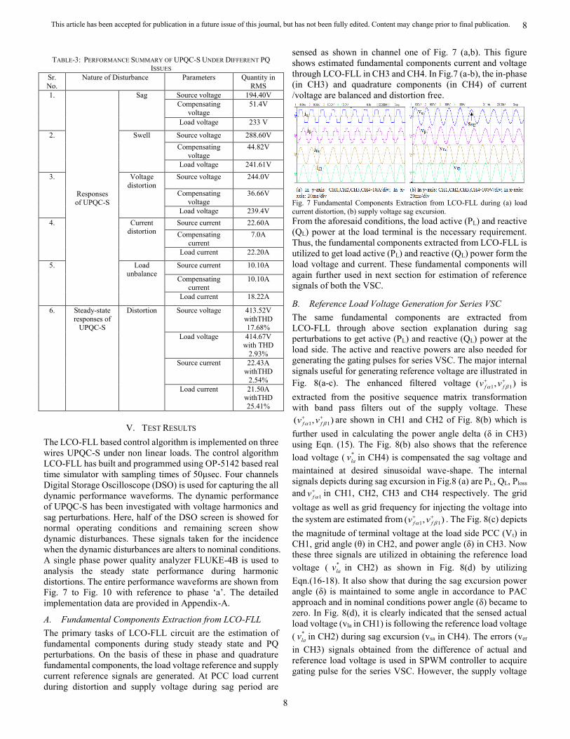
TABLE-3: PERFORMANCE SUMMARY OF UPQC-S UNDER DIFFERENT PQ
ISSUES
Sr.
No.
Nature of Disturbance Parameters Quantity in
RMS
1.
Responses
of UPQC-S
Sag Source voltage 194.40V
Compensating
voltage
51.4V
Load voltage 233 V
2. Swell Source voltage 288.60V
Compensating
voltage
44.82V
Load voltage 241.61V
3. Voltage
distortion
Source voltage 244.0V
Compensating
voltage
36.66V
Load voltage 239.4V
4. Current distortion
Source current 22.60A
Compensating
current
7.0A
Load current 22.20A
5. Load unbalance
Source current 10.10A
Compensating current
10.10A
Load current 18.22A
6. Steady-state
responses of UPQC-S
Distortion Source voltage 413.52V
withTHD 17.68%
Load voltage 414.67V
with THD
2.93%
Source current 22.43A
withTHD
2.54%
Load current 21.50A withTHD
25.41%
V. TEST RESULTS
The LCO-FLL based control algorithm is implemented on three
wires UPQC-S under non linear loads. The control algorithm
LCO-FLL has built and programmed using OP-5142 based real
time simulator with sampling times of 50μsec. Four channels
Digital Storage Oscilloscope (DSO) is used for capturing the all
dynamic performance waveforms. The dynamic performance
of UPQC-S has been investigated with voltage harmonics and
sag perturbations. Here, half of the DSO screen is showed for
normal operating conditions and remaining screen show
dynamic disturbances. These signals taken for the incidence
when the dynamic disturbances are alters to nominal conditions.
A single phase power quality analyzer FLUKE-4B is used to
analysis the steady state performance during harmonic
distortions. The entire performance waveforms are shown from
Fig. 7 to Fig. 10 with reference to phase ‘a’. The detailed
implementation data are provided in Appendix-A.
A. Fundamental Components Extraction from LCO-FLL
The primary tasks of LCO-FLL circuit are the estimation of
fundamental components during study steady state and PQ
perturbations. On the basis of these in phase and quadrature
fundamental components, the load voltage reference and supply
current reference signals are generated. At PCC load current
during distortion and supply voltage during sag period are
sensed as shown in channel one of Fig. 7 (a,b). This figure
shows estimated fundamental components current and voltage
through LCO-FLL in CH3 and CH4. In Fig.7 (a-b), the in-phase
(in CH3) and quadrature components (in CH4) of current
/voltage are balanced and distortion free.
Fig. 7 Fundamental Components Extraction from LCO-FLL during (a) load
current distortion, (b) supply voltage sag excursion.
From the aforesaid conditions, the load active (PL) and reactive
(QL) power at the load terminal is the necessary requirement.
Thus, the fundamental components extracted from LCO-FLL is
utilized to get load active (PL) and reactive (QL) power form the
load voltage and current. These fundamental components will
again further used in next section for estimation of reference
signals of both the VSC.
B. Reference Load Voltage Generation for Series VSC
The same fundamental components are extracted from
LCO-FLL through above section explanation during sag
perturbations to get active (PL) and reactive (QL) power at the
load side. The active and reactive powers are also needed for
generating the gating pulses for series VSC. The major internal
signals useful for generating reference voltage are illustrated in
Fig. 8(a-c). The enhanced filtered voltage1 1( , )f fv v
is
extracted from the positive sequence matrix transformation
with band pass filters out of the supply voltage. These
1 1( , )f fv v
are shown in CH1 and CH2 of Fig. 8(b) which is
further used in calculating the power angle delta (δ in CH3)
using Eqn. (15). The Fig. 8(b) also shows that the reference
load voltage (*
lav in CH4) is compensated the sag voltage and
maintained at desired sinusoidal wave-shape. The internal
signals depicts during sag excursion in Fig.8 (a) are PL, QL, Ploss
and1fv
in CH1, CH2, CH3 and CH4 respectively. The grid
voltage as well as grid frequency for injecting the voltage into
the system are estimated from1 1( , )f fv v
. The Fig. 8(c) depicts
the magnitude of terminal voltage at the load side PCC (Vt) in
CH1, grid angle (θ) in CH2, and power angle (δ) in CH3. Now
these three signals are utilized in obtaining the reference load
voltage (*
lav in CH2) as shown in Fig. 8(d) by utilizing
Eqn.(16-18). It also show that during the sag excursion power
angle (δ) is maintained to some angle in accordance to PAC
approach and in nominal conditions power angle (δ) became to
zero. In Fig. 8(d), it is clearly indicated that the sensed actual
load voltage (vla in CH1) is following the reference load voltage
(*
lav in CH2) during sag excursion (vsa in CH4). The errors (ver
in CH3) signals obtained from the difference of actual and
reference load voltage is used in SPWM controller to acquire
gating pulse for the series VSC. However, the supply voltage

This article has been accepted for publication in a future issue of this journal, but has not been fully edited. Content may change prior to final publication.
9
9
(vsa in CH4 during sag) is maintained respective reference
levels in CH2 by shunt VSC of UPQC-S.
Fig. 8 (a-d) Extraction of reference load voltage for series VSC
C. Dynamic Performance of UPQC-S
The dynamic performance analysis of UPQC-S for mitigating
the voltage harmonics and sags excursion using LCO-FLL
based control technique of “phase a” is explained from Fig. 9 to
Fig.10. The Fig.9 (a-b) shows the information about the supply
voltage (vsa), load voltage (vla), supply current (isa) and load
current (ila) during voltage harmonics distortions and sag
respectively. In these figures harmonic distortions of order 5th
and 7th and sag of 20% are superimposed on initial supply
voltages as depicted in Fig.9 (a) and Fig.9 (b) respectively. The
UPQC-S provides mitigation for harmonics distortions and
keeps load voltage distortion free as expressed in Fig.9 (a).
Also during sag excursion, the supply current magnitude is
increase due to variations in the supply voltages as seen in Fig.
9 (b) in third sub graph. At the same time load voltage is
maintained at sinusoidal nature with constant magnitude
irrespective of disturbances by UPQC-S. In Fig. 9(a,b), load
current (ila) is seem to be highly distorted and UPQC-S
maintained supply current (isa) is sinusoidal wave-shape. From
Fig. 9(a-b) during disturbances and nominal conditions the load
voltage (vla) in second sub graph are in-phase with the supply
current (isa) in third sub graph that indicates the UPQC-S is
maintain balanced voltage at unity power factor.
In Fig. 10(a-b) illustrates about the behavior of DC-link voltage
(Vdc in CH4) with supply voltage (vsa in CH1), load voltage (vla
in CH2), and compensating voltage of “phase a” (vca in CH3) at
the above-said PQ perturbations. It is noted that in Fig. 10(a-b)
the compensated voltage injected by series transformer is
in-phase during sag and harmonic distortions conditions. The
variations of DC bus voltage during the time of dynamic
disturbance can be observed in Fig. 10(a-b) in fourth sub graph
and it is noted that within one cycles the DC-link voltage is
settle at the desired level. All figures expressed that the
dynamic performance of the UPQC-S with LCO-FLL based
control algorithm is set up to compensating all PQ issues
successfully.
Fig. 9(a-b) Dynamic behavior of UPQC-S during (a) harmonics disturbances, (b) sag
Fig. 10(a-b) Dynamic behavior of UPQC-S during (a) Sag, (b) Harmonics with
DC link voltage
D. Steady State Performance Analysis of UPQC-S
The Fig.11 (a-h) illustrates the recorded waveform of phase a,
source current (isa), load current (ila), with supply voltage (vsa),
and load voltage (vla), under non-linear loads. These waveforms
are investigated during the supply voltage having 5th and 7th
harmonics distortions in the line. Fig. 11(a) shows the
waveforms of supply voltage (vsa) having voltage harmonics of
aforesaid conditions, and supply current (isa) after mitigation.
Fig. 11(b) leads to the information about distorted supply
voltage with 10.4% THD. After mitigation the supply current is
having RMS value 5.89A current with 4.6% THD which shows
in Fig.11(c). Similarly, Fig. 11(d) indicates the waveforms of
load voltage (vla) after compensation and distortional load
current (ila). It is observed in Fig. 11(e), the load voltage is
mitigated and having 63.2V RMS value and 3.7% THD.
However, a non linear load is considered having RMS value of
5.73A and 21.0% THD as shows in Fig. 11(f). One of the key
factors of UPQC is the load voltage (vla) and supply current (isa)
should be in same phase after the compensation that is depicts
in Fig. 11(g). At the same time load voltage and supply current
in Fig. 11(g) are near to sinusoidal in nature with desired
amplitude. From Fig. 11(c,e), it is clearly seen that the
waveform distortions in load voltage vla and supply current (isa)
are recorded under acceptable limit of IEEE-519-2014
standards. Fig. 11(h) indicates the waveforms of load voltage
(vla) after mitigation and compensator current of phase “a” (ica).

This article has been accepted for publication in a future issue of this journal, but has not been fully edited. Content may change prior to final publication.
10
10
Fig. 11 Steady state performance of UPQC-S (a) Distorted supply voltage (vsa),
compensated supply current (isa),(b) Harmonic spectrum of vsa (c)Harmonic spectrum of isa (d) Compensated load voltage (vla) and distorted load current (ila),
(e) Harmonic spectrum of vla(f) Harmonic spectrum of ila (g) Compensated,
load voltage (vla) and supply current (isa) (h)Compensator current (ica) with vla
However, the dynamic and steady-state performance of
UPQC-S using LCO-FLL control algorithm with power quality
disturbances in the system are given in Table-4.
TABLE-4: TEST PERFORMANCE OF UPQC-S
Sr.
No. Nature of Disturbance Parameters
Quantity in
RMS
1.
Dynamic responses
of
UPQC-S
Sag
Source voltage 51.5V
Compensating voltage 12.7V
Load voltage 63 V
2. Swell
Source voltage 77.2V
Compensating voltage 15.2V
Load voltage 63.5V
3. Voltage
distortion
Source voltage 63.5V
Compensating voltage 11.5V
Load voltage 63.5V
4. Current
distortion
Source current 8.85A
Compensating current 3.4A
Load current 5.65A
5. Load
unbalance
Source current 3.1A
Compensating current 3.0A
Load current 4.6A
6.
Steady-sta
te responses
of
UPQC-S
Distortion
Source voltage 63.7V with
THD 10.4%
Load voltage 63.2 V with
THD 3.7%
Source current 5.89 A with
THD 4.6%
Load current
5.73A
withTHD 21.0%
VI. CONCLUSIONS
The performance analysis of UPQC-S has been examined
under various practical power quality perturbations. The
response of LCO-FLL based control is found satisfactory
during transient and steady state condition. It is efficiently
estimating the time vary fundamental components from the
distorted supply. The series VSC shares significant amount of
through the shunt VSC which increases the utilization of series
transformer. Furthermore, efficiency is improved by using the
optimized values given by JAYA algorithm for PI-Controller
gains. Using JAYA, it is seen that the tuning speed of the
PI-Controller gains is enhanced from the conventional tuning
method. After 8th iterations, the PI-controller proportional gain
(Kp) and integral gain (Ki) are obtained 219.799, 26.63
respectively, which maintains dc bus voltage level to desired
magnitude. Now with these values, supply system with UPQC
has better settling time (ts) equal to 0.129sec, less peak over
shoot and tolerance band slightly less as compared to manual PI
gains value. By using the LCO-FLL and JAYA, the
performance of the three phase three wire UPQC-S is
significantly enhanced for reactive power compensation,
harmonic elimination, load unbalancing, voltage swells and
sags under load and supply variation.
APPENDIX
TABLE -5. SYSTEM PARAMETERS FOR UPQC-S
Parameter Simulation value Experimental value
PCC voltage (Vs) 415 V, 50 Hz 110 V, 50 Hz
Non-linear load: 3-ϕ bridge
rectifier
R=20 Ω, L=200
mH
R=20 Ω, L=200 mH
DC-link voltage (Vdc) 700 V 200 V
DC bus Capacitor (Cdc) 7000 μF 10000 μF
Injecting transformer 30/120 V, 4KVA 30/30 V, 2KVA
Source impedance (Zs) R=0.060 Ω R=0.060 Ω
L=2 mH L=2 mH
Shunt Interfacing inductance
(Lsh)
3mH 5.55 mH
Series Interfacing inductance
(Lse)
1.0 mH 2.0 mH
RC filter Rf=2.5 Ω Rf=5 Ω
Cf=20μF Cf=100μF
PI-Controller Kp=320 Kp=219.79
Ki=0.01 Ki=26.63
Switching frequency of VSCs (fs) 10 kHz 10 kHz
Sampling Time (ts) 10 μSec 50 μSec
LCO-FLL gains k= 0.1 k= 0.1
γ=-0.0351 γ=-0.0351
ACKNOWLEDGMENT
Authors thank the Science and Engineering Research Board
-New Delhi, India for supporting this work under the Grant No.
No.SB/S3/EECE/030/2016, Dated 17/08/2016
REFERENCES [1] K. R. Padiyar, FACTS Controllers in Power Transmission and
Distribution, New Age International, New Delhi, 2015. [2] E. W. Gunther and H. Mebta, “A survey of distribution system power
quality- preliminary results,” IEEE Transactions on Power Delivery,
vol. 10, no.1, pp.322-329, Jan. 1995. [3] D. Sabin and A. Sundaram, “quality enhances reliability,” IEEE
Spectrum, vol. 33, no.2, pp. 34-41, Feb. 1996
[4] Arindam Ghosh and Gerard Ledwich, Power Quality Enhancement Using Custom Power Devices, Springer International Edition, Delhi,
2009.
This article has been accepted for publication in a future issue of this journal, but has not been fully edited. Content may change prior to final publication.
11
11
[5] Inventor Gerardo, Escobar Alex Stankovic and Paolo Mattavelli,
“Adaptive controller for D-STATCOM in the stationary reference frame to compensate for reactive and harmonic distortion under
unbalanced conditions,” US Patent No. 2004/ 0071000 A1, Apr. 15,
2004. [6] S. Schneider and William E. Brumsickle, “Dynamic voltage sag
correction,” US patent No. 7920,392 B2, April 5, 2011.
[7] S. Bhattacharya and D. M. Divan, “Hybrid series active/parallel passive power line conditioner with controlled harmonic injection,”
U.S. Patent 5 465 203, Nov. 1995.
[8] L. Zhengfu, X. Baizhen, S. Chao, M. Ming, G. Wei,W. Hao, W. Minming and W. Ling, “Power unit commissioning system UPQC,”
CN Patent 203398792 Jul. 2013.
[9] B. Singh, A. Chandra, and K. Al-haddad, Power Quality Problems and Mitigation Techniques, John Wiley And Sons,UK, 2015.
[10] A. K. Panda and N. Patnaik, “Management of reactive power sharing
and power quality improvement with SRF-PAC based UPQC under unbalanced source voltage condition,” International Journal of
Electrical Power and Energy Systems, vol. 84, pp. 141-194, Jan. 2017.
[11] B. Gopal, P. K. Murthy and G.H. Sreenivas, “A review on UPQC for power quality improvement in distribution system,” Global Journal of
Researches in Engineering Electrical and Electronics Engineering.,
vol. 13, no. 7, version 1.0, pp. 41-49 May 2013. [12] S. Devassy and B. Singh,“ Dynamic performance of solar PV
integrated UPQC-P for critical loads” in Proc. Annual IEEE India
Conference( INDICON), pp. 1-6, New Delhi, Dec. 17-20, 2015. [13] M. Basu, S. P. Das and G. K. Dubey, “Investigation on the
performance of UPQC-Q for voltage sag mitigation and power quality improvement at a critical load point,” IET Generation, Transmission
and Distribution, vol. 2, no. 3, pp. 414-423, May 2008.
[14] G. S. Kumar, P. H. Vardhana, B. K. Kumar and M. K. Mishra, “Minimization of VA loading of Unified Power Quality Conditioner
(UPQC),” in proc. International Conference on Power Engineering,
Energy and Electrical Drives, pp. 552-557, Lisbon, 18-20 Mar. 2009. [15] Quoc-Nam, Trinch and Lee Hong Hee, “Improvement of unified
power quality conditioner performance with enhanced resonant
control strategy,”IET Generation, Transmission and Distribution, vol. 8, no. 12, pp. 2114-2123, Dec.2014.
[16] Z. Miao, L. Deliang, T. Xiongmin and Y. Yufeng, “Control algorithm
for single-phase unified power quality regulator,” CN Patent 105680451 Mar. 2016.
[17] V. Khadkikar, A. Chandra, A. O. Barry and T. D. Nguyen, “Power
quality enhancement utilising single phase unified power quality conditioner: digital signal processor based experimental validation,”
IET Power Electronics, vol. 4, no. 3, pp. 323-331, Mar. 2011.
[18] H. Akagi, Y. Kanazawa and A. Nabae, “Instantaneous reactive power compensators comprising switching devices without energy storage
components,” IEEE Transactions on Industry Applications, vol. IA-20,
no. 3, pp. 625-630, May 1984. [19] Pengcheng Zhu, Xun Li, Yong Kang and Jian Chen, “A novel control
scheme in 2-phase unified power quality conditioner,” in Proc.
29thAnnualConference of the IEEE Industrial Electronics Society, vol. 2, pp. 1617-1622, Roanoke VA,USA, Nov. 2-6, 2003.
[20] V. Khadkikar, P. Agarwal, A. Chandra, A. O. Barry and T. D. Nguyen,
“A simple new control technique for unified Power quality conditioner (UPQC),”in Proc. 11thInternational Conference on Harmonics and
Quality of Power, pp. 289-293, Lake Placid NY, USA, Sep. 12-15,
2004. [21] L. P. Kunjumuhammed and M. K. Mishra, “A control algorithm for
single phase active filter under non stiff voltage source,” IEEE
Transactions on Power Electronics, vol. 21, no. 3, pp. 822-825, May 2006.
[22] M. Karimi-Ghartemani, H. Mokhtani, M. R. Iravani and M. Sedighy,
“A signal processing system for extraction of harmonics and relative current of single phase systems,” IEEE Transactions on Power
Delivery, vol.19, no. 3, pp. 979-986, July 2004.
[23] S. Golestan, J. M. Guerrero and J. C. Vasquez, “Three phase PLLs: A review of recent advances,” IEEE Transactions on Power Electronics,
vol. 32, no. 3, pp. 1894-1907, Mar. 2017.
[24] L. Hadjidemetriou, E. Kyriakids, Y Yang and F. Blaabjerg,“A synchronization methods for single phase grid tied inverter,” IEEE
Transactions on Power Electronics, vol. 31, no. 3, pp. 2139-2149, Mar.
2016. [25] E. Oviedo, N. Vazquez and R. Femat, “Synchronization technique of
grid connected power converter based on a limit cycle
oscillator,”IEEE Transactions on Industrial Electronics, vol. 65, no. 1,
pp. 709-717, Jan. 2018. [26] P. Rodriguez, A. Luna, I. candela, R. Mujal, R. Teodorescu and F.
Blaabjerg, “Multi-resonant frequency locked loop for grid
synchronization of power converter under distorted gird conditions,” IEEE Transactions on Industrial Electronics, vol. 58, no. 1, pp.
127-138, Jan. 2011.
[27] H. K. Khalil and J.W. Grizzle, Nonlinear systems, vol. 3, Upper Saddle River, NJ, Prentice hall, 2002.
[28] P. Cominos and N. Munro, “PID controllers: recent tuning methods
and design to specification,” IEEE Proceedings- Control Theory and Applications, vol. 149, no. 1, pp. 46-53, Jan 2002.
[29] K. Kalpana and B. Meenakshipriya, “Design of coefficient diagram
method (CDM) based PID controller for double integrating unstable system,” in Proc. IEEE 2nd International Conference on Electrical
Energy Systems (ICEES), pp. 189-193, Chennai, India, Jan.7-9, 2014.
[30] H. Wu, W. Su and Z. Liu, “PID controllers: Design and tuning methods,” in Proc. IEEE 9th IEEE Conference on Industrial
Electronics and Applications, pp. 808-813, Hangzhou, China, Jun.
9-11 2014. [31] R. V. Rao, V. J. Savsani and D. P. Vakharia, “Teaching learning based
optimization: A novel method for constrained mechanical design
optimization problems,” Journal of Computer Aided Design, vol. 43, no. 3, pp. 303-315, Mar. 2011.
[32] R. V. Rao, “JAYA: A simple and new optimization algorithm for
solving constrained and unconstrained optimization problems,” International Journal of Industrial Engineering Computations, vol. 7,
no. 1, pp. 19-34, Aug. 2016. [33] J. Blackburn, Symmetrical Components for Power Systems
Engineering, New York, USA, Marcel Dekkar, 1993
[34] Gopal Madan, Digital Control and State Variables Methods: Conventional and Intelligent Control Systems, New Delhi, Tata
McGraw-Hill Education, 2012.
BIOGRAPHIES Sabha Raj Arya (M’12, SM’15) received
Bachelor of Engineering degree in Electrical
Engineering from Government Engineering College Jabalpur, in 2002, Master of Technology
in Power Electronics from Motilal National
Institute of Technology, Allahabad, in 2004 and
Ph.D. degree in Electrical Engineering from
Indian Institute of Technology (I.I.T) Delhi, New
Delhi, India, in 2014. He is joined as Assistant Professor, Department of Electrical Engineering,
Sardar Vallabhbhai National Institute of
Technology, Surat. January 2019, he is promoted as Associate Professor in same institute. His fields of interest include Power electronics, power quality,
design of power filters and distributed power generation.
He received Two National Awards namely INAE Young Engineer Award from Indian National Academy of Engineering, POSOCO Power System Award
from Power Grid Corporation of India in the year of 2014 for his research work. He is also received Amit Garg Memorial Research Award-2014 from I.I.T
Delhi from the high impact publication in a quality journal during the session
2013-2014. At present, he has published more than Hundred research paper in internal national Journals and conferences in field of electrical power quality.
He also serves as an Associate Editor for the IET (U.K.) Renewable Power
Generation.
Sayed Javed Alam received the Bachelor of Technology in Electrical
Engineering from Rajasthan Institute of Engineering & Technology Jaipur, India, in 2012 and M.Tech degree in electrical engineering with specialization
in power electronics and electrical drives from Birla Institute of Technology,
Mesra, India in 2015. In February 2016, he joined the department of electrical engineering, Global Institute of Technology, Jaipur, India, as an Assistant
Professor. From July 2017 onwards, he is
currently pursuing the Ph.D. degree in electrical engineering from Sardar Vallabhbhai National
Institute of Technology Surat, India. His research
area includes power electronics, power quality and design of custom power devices, multilevel
inverter and dc-dc converters.

This article has been accepted for publication in a future issue of this journal, but has not been fully edited. Content may change prior to final publication.
12
12
Papia Ray (M’13, M’19) received her Bachelor
of Engineering (Electrical Engineering) degree from Government Engineering College, Bihar
followed by Master of Technology (Power
Systems) from National Institute of Technology, Jamshedpur and Ph.D degree from Indian Institute
of Technology, Delhi in 2013. She is presently
serving as Associate Professor in Electrical Engineering Department of Veer Surendra Sai
University of Technology (Govt. Univ), Burla,
Odisha. She has more than 18 years of teaching experience. She has 45 research publications in
journals like IET, Elsevier, Wiley etc. She is a senior member of IEEE, member
of Institution of Engineers and Life Member of ISTE. She is the recipient of Young Scientist Award from DST in the year 2015. Her research interest
includes power system protection, wide area Measurement systems, biomedical
engineering etc.