contract no. n00014-85-k-0619 arlington, virginia … electromagnetic communication laboratory...
TRANSCRIPT

PULSE PROPAGATION INHIGH-SPEED DIGITAL CIRCUITS
Co0NFINAL REPORT
O for
Contract No. N00014-85-K-0619
Office of Naval ResearchDepartment of the Navy800 North Quincy Street
Arlington, Virginia 22217
S MA17 1989 IJPrepared by
R. Mittra
Electromagnetic Communication LaboratoryDepartment of Electrical and Computer Engineering
Engineering Experiment StationUniversity of Illinois at Urbana-Champaign
Urbana, Illinois 61801-2991
u-: h o-N T7_:M H rr A
May 1989

UILU-ENG-89-2541
Electromagnetic Communication Laboratory Report No. 89-3
PULSE PROPAGATION INHIGH-SPEED DIGITAL CIRCUITS
Final Report
for
Contract No. N00014-85-K-0619
Office of Naval ResearchDepartment of the Navy -800 North Quincy Street
Arlington, Virginia 22217
May 1989
-1
Prepared by A-1R. Mittra
Electromagnetic Communication LaboratoryDepartment of Electrical and Computer Engineering
Engineering Experiment StationUniversity of Illinois at Urbana-Champaign
Urbana, Illinois 61801-2991

UNCLASSIFIEDSECURITY CLASSIFICATION OF TIS PAGE
REPORT DOCUMENTATION PAGEla REPORT SECURITY CLASSIFICATION lb. RESTRICTIVE MARKINGS
2a. SECURITY CLASSIFICATION AUTHORITY 3 DISTRIBUTION/AVAILABLiTY OF REPORT
2b. OECLASSIFiCATION/DOWNGRADING SCHEDULE UNLLMITED4 PERFORMING ORGANIZATION REPORT NUMBER(S) 5. MONITORING ORGANIZATION REPORT NUMBER(S)
UILU-ENG-89-2541
EMC 89-3
6a. NAME OF PERFORMiNG ORGANIZATION 6o. OFFICE SYMBOL 7a. NAME OF MONITORING ORGANIZATIONUniversity of Illinois (If applicable) Office of Naval Research Detachmentat Urbana-Champaign Chicago
6 . ADDRESS (City, State, and ZIPCode) 7b. ADDRESS (City, State, and ZIP Code)1406 W. Green St. 536 S. Clark St.
Urbana, IL 61801 Chicago, IL 60605-1588
"a. NAME OF ;UNDING/SPONSORING 8b. OFFICE SYMBOL 9 PROCUREMENT INSTRUMENT IDENTIFICATION NUMBER
ORGANIZATION Department of Navy (if applicable)
Office of Nalal Research I8c. ADDRESS (City, State. and ZIP Code) 10. SOURCE OF FUNDING NUMBERS
800 N. Quincy St. PROGRAM PROJECT TASK IWORK UNITELEMENr NO NO NO ACCESSION NOArling-ton, VA NR 613-006 r
I1 TlTLE (include Secunty Classfication)
PULSE PROPAGATION IN HIGH-SPEED DIGITAL CIRCUITS
2 ERSONAL AUTHOR(S)R. Mittra
13a. TvDE OF REPORT 13b. TIME COVERED 14. DATE OF REPORT (Year, Month, Day) IS PAGE COUNTFinal"I FROM5-3-85 T04-31-89 May 8, 1989 122
.6 SuPPLEMENTARY NOTATION
COSATI CODES 18. SUBJECT TERMAS (Continue on reverse if necessary and identify by block number);IELD GROUP SUB-GROUP Digital circuits, Pulse propagation, Electromagnetic
modeling, Printed circuit boards, Microstrip lines anddiscontinuities
'9 AB5TRACT (Continue on reverse if necessary and identify by block number)
In this effort, we have developed several techniques for the computation of theharacteristic impedance as well as capacitance and inductance matrices for a number of
different types of transmission-line constructions, e.g., stripline, microstrip line,buried microstrip line and orthogonal line. We have also investigated methods for
measuring the high frequency characteristics of planar transmission lines which may, ingeneral, be lossy. The capacitance and inductance matrices have been employed in a computer
program that analyzes an n-line system terminated with digital devices, both for the loss-less and lossy cases.
The fi rite element methoA and the method of moments have been applied to the problem
of computing the equivalent circuits of connectors, interconnects and other discontinuities
in planar transmission lines, e.g., the bend, the tapered line and the through-hole via.(continued on back...)
20 DISTRIBUTION/ AVAILABILITY OF ABSTRACT 21. ABSTRACT SECURITY CLASSIFICATION
0 UNCLASSIFEDi'UNLIMITED 0l SAME AS RPT. rl DTIC USERS Unclassified
22a 14AME OF RESPONSIBLE INDIVIDUAL 22b TELEPHONE (Include Area Code) 22c. OFFICE SYM8OL
R. Mittra 217-333-1202
DO FORM 1473,84 MAR 83 APR edition may oe used until exhausted. SECURITY CLASSIFICATION OF THIS PAGEAll other editions are obsolete UNCLASSIFED

UNCLASSIFIED,9CURITY CLASSIICATIOM OF T41, 0AGE
19. Abstract (continued)
These equivalent circuits have been used to predict the pulse propagation in pc boards
involving sections of uniform lines combined with discontinuities mentioned above.
UNCLASSIFIED
SeCUPITY CLASSIFICATION OF rNIS PACE

iv
TABLE OF CONTENTS
Page
I. INTRO DU CTIO N ........................................................................ I
II. PERSONNEL ........................................................................... 1
III. TECH N ICA L ................................................ . . ................... 1
A. QUASISTATIC AND FREQUENCY-DEPENDENTANALYSIS OF DIFFERENT TRANSMISSION-LIKECONFIGURATIONS ......................................................... 1
B. FINITE ELEMENT ANALYSIS OF TRANSMISSION LINES ..... 2
C. PULSE PROPAGATION AND CROSSTALK INMULTICONDUCTOR LINES WITH LOSSES ............................ 2
D. CONNECTOR, INTERCONNECT ANDDISCONTINUITY MODELING .............................................. 3
IV . REFEREN CES ........................................................................... 5
APPENDIX A *
AN ABSORBING BOUNDARY CONDITION FOR QUASI-TERMANALYSIS OF MICROWAVE TRANSMISSION LINES VIATHE FINITE ELEMENT METHOD by A. Khebir, A. B. Kouki, and R. Mittra
APPENDIX B *
TRANSIENT ANALYSIS OF LOSSY MULTICONDUCTORTRANSMISSION LINES IN NONLINEAR CIRCUITSby T. S. Blazeck and R. Mittra
APPENDIX C *
SCATTERING PARAMETER TRANSIENT ANALYSIS OFTRANSMISSION LINES LOADED WITH NONLINEARTERMINATIONS by J. E. Schutt-Aine and R. Mittra
* (All appendices have their own pagination.)

I. INTRODUCTION
This final report summarizes the progress made on research related to the problem of
"Pulse Propagation in High Speed Digital Circuits" covering the period of September 1, 1985 to
March 31, 1989.
II. PERSONNEL
Dr. R. Mittra, Professor of Electrical Engineering
Dr. C. Cnan, Visiting Assistant Professor
Mr. J. Schutt-Aine, Visiting Assistant Professor
Dr. Z. Pantic, Research Associate
Mr. A. Ali, Air Force Fellow
Mr. Paul Aoyagi, Graduate Teaching Assistant
r. T. Blazeck, Graduate Research Assistant
Mr. S. Castillo, Graduate Research AssistantMr. Woo-Sung Chi, Graduate Teaching Assistant
Mr. U. Feldman, Graduate Research Assistant
Mr. P. Harms, Graduate Research Assistant
Mr. A. Khebir, Graduate Research Assistant
Mr. A. Kouki, Graduate Student
Mr. M. Mehalic, Air Force Fellow
Mr. G. Salo, Graduate Research Assistant
Mr. J. Sutton, Graduate Research Assistant
Mr. G. Wilkins, Graduate Student Fellow
III. TECHNICAL
A. QUASISTATIC AND FREQUENCY-DEPENDENT ANALYSIS OF DIFFERENT
TRANSMISSION-LINE CONFIGURATIONS
We have developed techniques for the computation of the characteristic impedance as well
as capacitance and inductance matrices for a number of different types of transmission-line
constructions, e.g., stripline, microstrip line, buried microstrip line and orthogonal line. The

2
numerical techniques we have employed employ the FFT algorithm combined with the iterative
techniques and are considerably more efficient than those based upon the conventional moment
method that require the inversion of large matrices. The algorithms have been extended to the
frequency-dependent case by using full-field solution of Maxwell's equations, rather than the
quasi-static approximation.
We have also investigated two experimental techniques for measuring the high frequency
characteristics of planar transmission lines which may, in general, be lossy. In this approach, the
line parameters, viz., R, L, G and C,are obtained by using an algorithm for reducing these
parameters from the S-parameter measurements carried out with a Network Analyzer.
B. FINITE ELEMENT ANALYSIS OF TRANSMISSION LINES
We have developed a general purpose, finite element (FEM) analysis which is capable of
handling transmission lines of arbitrary cross-section and with arbitrary fillings. The FEM program
requires a mesh generation algorithm. A simple mesh program, that is portable in nature, was
developed by us for use with the program. However, we have found that it is more expedient to
acquire a commercial version of the mesh generation program, e.g., PATRAN, and combine it
with our FEM programs for solving either Laplace's or Maxwell's equations.
The FEM approach calls for a method for mesh truncation whenever open-region problems
are analyzed using this method. We have developed an absorbing boundary condition for mesh
truncation and have applied it to single and multi-conductor transmission lines. The approach is
described in Attachment A.
C. PULSE PROPAGATION AND CROSSTALK IN MULTICONDUCTOR LINES
WITH LOSSES
We have generalized the analysis of lossless n-lines, terminated with digital devices, to the
lossy case using two different approaches. In the first approach, the frequency-domain Gicen's
function method is used in the transmission line part of the circuit, which is linear, in conjunction

3
with a nonlinear analysis of the terminating circuits, that include digital devices, directly in the time
domain. The line is characterized by per unit values of resistance (r), inductance (1), conductance
(g) and capacitance (c). If desired, r can be made to vary with frequency to model the skin effect
and g can also be a variable of frequency. The terminal networks that model the nonlinear digital
devices consist of capacitors in parallel with nonlinear voltage-controlled resistors.
We have prepared a report (see Attachment B) describing this analysis and have appended it
herewith.
The second approach we have developed for the time-domain simulation of n-line
structures terminated by logic gate inverters, is based on a state-space approach employed in
conjunction with the Scattering Matrix representation of the coupled n-lines. It is designed to treat
both the lossless and lossy line cases and has been described in a recent publication a copy of
which is appended in Attachment C.
D. CONNECTOR, INTERCONNECT AND DISCONTINUITY MODELING
The finite element method, as well as other analytical and numerical techniques, are being
investigated with the objective of modeling connectors, interconnects and discontinuities
introduced by a change in the conductor width or the presence of a stub, etc. In general, the
connector, the via, and similar other discontinuity problems must be modeled by using a three-
dimensional mesh generation program: hence, such modeling is computer intensive. The
connector problem has been investigated using the full 3-D mesh and with an approximate 2-D
model. It has been shown that in some cases it is possible to use the 2-D approximation, though
this is not universally true. A comprehensive report on the connector that describes the analysis,
numerical results and the experimental verification of these results has been prepared and a paper
summarizing the research has been submitted for publication.
An alternative approach, based on the method of moments (MoM) has been employed for
both the bend and the via problems. Numerical results for the inductance and capacitance matrices
have been obtained for the single and multiple line bends in microstrip lines. The modeling of of

4
the via problem is being continued.
Another discontinuity problem being investigated in this effort is the tapered-line problem,
which arises in the modeling of interconnects, and has been analyzed using a perturbational
approach. Both single and multiple lines with arbitrary tapers have been investigated using the
scattering matrix approach. Experimental verification of the theoretical results is currently being
carried out.

5
IV. REFERENCES
Journal Articles
1. Jose E. Schutt-Aine and R. Mittra, "Analysis of pulse propagation in coupled transmissionlines," IEEE Trans. on Circuits and Systems, vol. CAS-32, no. 12, pp. 1214-1219,December 1985.
2. R. Mittra and C. Chan, "Iterative approaches to the solution of electromagnetic boundaryvalue problems," Electromagnetics, vol. 5, no. 2-3, pp. 123-146, 1985.
3. E. Farr, C. Chan and R. Mittra, "A frequency-dependent coupled-mode analysis ofmulticonductor microstrip lines with application to VLSI interconnection problems," IEEETrans. on Microwave Theory and Techniques, vol. MTT-34, no. 2, pp. 307-310,February 1986.
4. Z. Pantic and R. Mittra, "Quasi-TEM analysis of microwave transmission lines by thefinite-element method," IEEE Trans. on Microwave Theory and Techniques, vol. MT'I-34,no. 11, pp. 1096-1103, November 1986.
5. C. H. Chan and R. Mittra, "Analysis of a class of cylindrical multiconductor transmissionlines using an iterative approach," IEEE Trans. on Microwave Theory and Techniques,vol. MTT-35, no. 4, pp. 415-424, April 1987.
6. C. H. Chan and R. Mittra, "Comparative study of iterative techniques, moment method andspectral Galerkin approach for solving the problem of electro-magnetic scattering by arectangular plate," IEE Fifth International Conference on Antennas and Propagation ICAP87, pp. 443-446, held in York, March 30 - April 2, 1987.
7. C. Chan and R. Mittra, "Analysis of MMIC structures using an efficient iterativeapproach." IEEE Trans. Mirowave Theory & Techniques, vol. MTT-36, no. 1, pp. 96-105, January 1988.
8. J. E. Schutt-Aine and R. Mittra, "Scattering parameter transient analysis of transmissionlines loaded with nonlinear terminations," IEEE Trans. Microwave Theory & Techniques,vol. MTT-36, no. 3, pp. 529-536, March 1988.
9. C. H. Chan and R. Mittra, "The propagation characteristics of signal lines embedded in amultilayered structure in the presence of a periodically perforated ground plane," IEEETrans. Microwave Theory & Techniques, vol. MTT-36, no. 6, pp. 968-975, June 1988.
10. Z. Pantic and R. Mittra, "Calculation of characteristic impedance of planar, inhomogeneoustransmission lines for digital circuit applications," AEU, Band 42, Heft 5, pp. 325-327,Sept./Oct. 1988.
11. Q. Xu, K. J. Webb and R. Mittra, "Study of modal solution procedures for microstrip stepdiscontinuities." IEEE Trans. Microwave Theoy and Techniques, vol. MTT-37, no. 2,pp. 381-387, February 1989.

6
Technical Reports
1. U. Feldman and R. Mittra, "Characterization of microstrip discontinuities," EMCTechnical Report, No. 85-6, University of Illinois, September 1985.
2. G. R. Salo and R. Mittra, "The modeling of connectors for printed circuit boards," EMCTechnical Report, No. 85-7, University of Illinois, October 1985.
3. Z. Pantic and R. Mittra, "Quasi-TEM analysis of microwave transmission lines by thefinite-element method," DAAG 29-85-K-0183, EMC Report No. 86-2, February 1986.
4. A. S. Ali and R. Mittra, "Time-domain reflectometry using scattering parameters and a de-embedding application," N00014-85-K-0619, EMC Report No. 86-4, May 1986.
5. J. R. Sutton and R. Mittra, "Computer-aided design of nonlinear networks with N-conductor transmission lines systems," N00014-85-K-0619 and Fellowship Grant fromNorthrop Corporation , EMC Report No. 86-8, November 1986.
6. P. H. Harms and R. Mittra, "Modeling of planar transmission line structures for digitalcircuit applications," N00014-85-K-0619, EMC Report No. 86-9, November 1986.
7. Z. Pantic and R. Mittra, "Full-wave analysis of isolated and coupled microwavetransmission lines using the finite element method," DAAG29-85-K-0183, EMC ReportNo, 87-i, February 1987.
8 J. E. Schutt-Aine and R. Mittra, "Scattering parameter transient analysis of transmissionlines loaded with nonlinear terminations," N00014-85-K-0619, EMC Report No. 87-2,March 1987.
9. S. P. Castillo and R. Mittra, "Electromagnetic modeling of high-speed digital circuits,"N00014-85-K-0619, EMC Report No. 87-3, June 1987.
To Be Published
1. S. P. Castillo and R. Mittra, "Analysis of N-conductor transmission line system terminatedwith non-linear digital devices," submitted to Electromagmetic Compatibility
2. S. Castillo, Z. Pantic and R. Mittra, "Finite element analysis of multiconductor printedcircuit transmission lines systems," submitted to MI'.

7
Thesis
1. "The modeling of connectors for printed circuit boards," Glen R. Salo, M.S. Thesis, May1985.
2. "Characterization of microstrip discontinuities in the time and frequency domains," UriFeldman, M. S. Thesis, June 1985.
3. * ime-domain reflectometry using scattering parameters and a de-embedding application,"Azar Ali, M. S. Thesis, May 1986.
4. "Computer-aided design of ncnlinear networks with N-conductor transmission linesystems," J. R. Sutton, M. S. Thesis, November 1986.
5. "Modeling of planar transmission line structures for digital circuit applications," P. H.Harms, M. S. Thesis, November 1986.
6. "Investigation of Iterative and spectral Galerkin Techniques for Solving ElectromagneticBoundary Value Problems," C. H. Chan, Ph.D. Thesis, May 1987.
7. "Electromagnetic Modeling of High-Speed Digital Circuits," S. P. Castillo, Ph.D. Thesis,May 1987.
8. "Transient Analysis of Lossy Multiconductor Transmission Lines in Nonlinear Circuits,"T. S. Blazeck, Ph.D. Thesis, May 1989.

APPENDIX A

AN ABSORBING BOUNDARY CONDITION
FOR QUASI-TEM ANALYSIS OF MICROWAVE
TRANSMISSION LINES VIA THE FINITE ELEMENT
METHOD
A. Khebir, A. B. Kouki, and R. Mittra
Electromagnetic Communication Laboratory
Electrical & Computer Engineering Department
University of Illinois
Urbana, IL 61801
Abstract
Open microwave transmission line structures are analyzed in this paper in the quasi-
TEM regime using the finite element method. An absorbing boundary condition(ABC) for an
arbitrary outer boundary is introduced for the purpose of truncating the unbounded region
surrounding the transmission line in an efficient manner. The application of the boundary
condition is illustrated for three different microstrip line configurations, viz., a single line, two
coupled lines, and a six-conductor line. Numerical results are compared with those published
elsewhere and good agreement is found.

2
I. Introduction
Microwave transmission lines have been investigated by many researchers who have
employed a variety of methods to study the problem of computing the characteristic impedance
and propagation constant along these lines. Some of these techniques include the Fourier
transform method [1-2], variational method (3-4], spectral domain method [5-7], Green's
function technique [8-13], conformal mapping [14-16], boundary element method [17-18], and
finite-element method [19-20]. All but the last two approaches mentioned above are limited to
thin strips and/or to structures containing dielectrics with planar interfaces. Although the finite
element method method (FEM) is very general, and can handle any arbitrary configuration of
conductors and dielectrics, it must deal with the practical problems of mesh truncation and the
need for a large number of mesh nodes when applied to an open region problem. One approach
to circumventing this difficulty is to truncate the mesh by introducing a fictitious conducting
enclosure[ 19, 21]. This approach yields satisfactory results only if the actual field decays
sufficiently well as it reaches the outer boundary. Typically, this requires one to recede the
outer boundary far away from the structur-, in order to achieve acceptable accuracy and, this, in
turn, results in a large mesh. An alternative approach is to use "infinite" elements (201, that
extend to infinity, and cover the region outside of a fictitious boundary surrounding the
structure. Although superior to the artificial p.e.c boundary method, this approach nonetheless
has its own drawbacks. First, the infinite elements require special care during the filling of the
FEM matrix. Second, one needs to assume a certain asymptotic behavior of the field within the
infinite elements, and this behavior may not be convenient to obtain.
In this paper, we introduce an absorbing boundary condition(ABC) which provides us
with an efficient means for dealing with the open region problems in the quasi-static regime.
This absorbing boundary condition does not suffer from the complications associated with the
infinite elements, and yet enables us to bring the outer boundary much closer to the structure

3
than would be possible with the p.e.c. artificial boundary. Furthermore, unlike many of the
available ABC's that are restricted to separable outer boundaries, the one presented in this
paper is useful for an arbitrarily-shaped outer boundary. We will demonstrate the versatility of
this new absorbing boundary condition by considering the examples of one, two, and six
conductor microstrip lines.
II. Derivation of the Absorbing Boundary Condition
Figure 1 depicts the geometry of an open region problem consisting of N arbitrarily-
shaped conductors embedded in a multilayered medium above a ground plane. Let OlT denote
the region exterior to the conductors. For the finite mathematics techniques [22-23], the
unbounded outer region 2T must be truncated and enclosed with an outer boundary 12 . The
strategy for deriving an absorbing boundary condition is to find an operator which, when
applied on the outer boundary, would mimic the asymptotic behavior of the wave function at
ty and would thus yield accurate results in the interior region without the need of an
exorbitantly large number of mesh points. The problem at hand can be described in terms of
the following set of equations:
V2 u = 0 in L.r (1)
u = gi on the i conductor (2)
Bmu = 0 on r 2 (3)
where u is the potential function and Bm is the mth order absorbing boundary condition
operator.
An asymptotic form of the solution, valid for large p can be written as:
u(p,4) = 'an cosno (4)n=1 P

4
Equation (4) can be used to obtain an absorbing boundary condition on an artificial boundary.
Manipulating (4) one can obtain the first-order absorbing boundary condition operator, which
reads
u B1u = r; + - " 7 (
Similarly, the second-order absorbing boundary condition operator takes the form
B~u + 3 )(ju + 2_) = (6)
As will be seen later, the finite element formulation of the problem involves an integral over the
outer boundary, F2 , and the normal derivative of u appears in this integrand. Hence, for our
purposes, it it is more desirable to find an asymptotic representation for the normal derivative
of u rather than make direct use of the operator B2. For a circular outer boundary, the normal
derivative will simply be the radial one which can readily be obtained from (6). Mittra and
Ramahi [30] have presented a procedure for deriving an absorbing boundary condition operator
for the dynamic case in terms of the field and its second-order angular derivative that can be
conveniently adapted to the quasi-static case of interest here. We begin by expressing the radial
derivative of u in a manner similar to the one described in [30]. Next, we use (1) to exchange
the second-order derivative in p, upp, with the second-order angular derivative, u", to obtain
the desired absorbing boundary condition:
up = a(p) u + 3(p) u0 (7)
where a(p) and 5(p) are given by
_CP) = -2L (8)
P(): 1 (9)

For a general, noncircular outer boundary it is necessary to generalize (7) and derive an
expression for the normal derivative operator un in the local coordinate system (t,n) where t and
n are tangent and normal to the boundary, respectively. An approximate expression for this
derivative can be obtained by following the procedure described in [24] and is given by
n =u+ u + 3 un (10)
where
a (x0 sinO0 - yo cosO ( 3p(
1 2 2-t (xo sine o -yo cosO0 ) + 'sin2 0 o (yo -xo) +xoyo cos20o
2 (12)P
ok p)
=(xO sine0 -yo cosO0)~ p (13)
= 4 t2 +x + Y2 + 2t (xocos0o +yosin 0 o) (14)
and 00, xO, yo, and t are as shown in Fig. 2.
III. Finite Element Implementation of the Absorbing Boundary Condition
The problem at hand is to solve for the potential u satisfying the Laplace's equation:
V'(eVu) = 0 (15)
Multiplying (15) by a testing function v and integrating over the domain of the problem
OT, we obtain
SO. v V'(F.Vu) ds = 0 (16)

From Green's identity we have
V'(eVu) ds = -4 Vu'Vv ds + v e--u dt (17)
Inserting the above in (16), we get
SeVu'Vv ds = v dt (18)
In the finite element formulation, one sets up a mesh in the region UT, typically using
triangular elements. The edges of the outermost elements prescribe 172 . Hence, considering
one element at a time, the absorbing boundary condition given in (10) may be incorporated into
(18) to yield
S Vu-Vv ds= ve( u+y ut+P utt)dt (19)
2
Since e is constant over each element, we can integrate (19) by parts to obtain
JeVu-Vv ds =f e (a vu + Y vuJ - vtu t - _" vu,) dt (20)2
where
= (xOsin 0o-yOcose0o)(t + xOcos0o+Yosin0o) 4 (21)
The form given in (20) is well-suited for numerical implementation for any arbitrary
conductor configuration enclosed by any arbitrarily-shaped outer boundary.

IV. Numerical Results
a. One Conductor
The microstrip line, shown in Fig. 3, is enclosed by a rectangular outer boundary. We
first solved the potential problem by applying the absorbing boundary condition, given in
equation (7), on a rectangular outer boundary. Next, we introduced a perfectly electric
conducting shield at the outer boundary and solved the problem once again using the same
mesh. As Table 1 indicates, the relative error between the absorbing boundary condition and
the published results (12, 26, 271 is between 0.053 and 2.56 percent, whereas the error
between the shield and the published results is between 14.55 and 30.04 percent.
b. Two conductors:
Two coupled microstrips, shown in Fig. 4, are enclosed by a rectangular outer
boundary. Table 2 presents some results for the same problem that have been published
elsewhere[12, 28, 29], together with those obtained by using a p.e.c. shield and the absorbing
boundary condition in (10). The relative error in the self-terms is 0.27 percent for the
absorbing boundary condition and 18.31 percent for the shield. Likewise, the error in the
mutual terms is 5.2 percent for the absorbing boundary condition and 44.59 percent for the
shield.
c.Six conductors:
The six conductor system, shown in Fig. 5, is enclosed, once again, by a rectangular
outer boundary. To the best of our knowledge, there are no published results for this
configuration. However, we have compared our results with those derived oy using tne
computer program developed by Chan [25], which uses an integral equation formulation and
an iterative method of solution. As Table 3 indicates, the relative error for the capacitance
matrix is between 0.84 and 14.52 percent for the absorbing boundary condition and between

3.96 and 74.10 percent for the p.e.c shield when compared to the results obtained with the
iterative solution. For the inductance matrix, the error is between 0.02 and 11.46 percent for
the absorbing boundary condition and between 39.74 and 96.72 percent for the p.e.c shield.
In addition, the relative error between the absorbing boundary condition and the shield reached
69.69 percent in the capacitance matrix and 97.01 percent in the inductance matrix.
In all of the three numerical examples considered thus far, we have chosen a rectangular
outer boundary because it facilitates the meshing procedure and because it is conformal to the
structures considered. This meshing is done in a manner such that none of the triangular
elements have more than one edge on the outer boundary. Since the finite element scheme
considers one element at a time, the problem of the undefined normal at the rectangular corners
is circumvented when the procedure described above is followed.
In order to illustrate the fact that the formulation described in this paper is also
applicable to an arbitrary outer boundary, we reconsider the two-conductor example described
earlier. Figure 6 illustrates the coupled microstrips problem with an arbitrary outer boundary.
Table 4 shows that the results obtained for this case are almost identical to those derived with
the rectangular boundary.
Finally, before closing, we point out that no special treatment is needed at the dielectric
interfaces because in the finite element formulation the medium is modeled as being
homogeneous within each element and, consequently, the line integral in equation (20) is
always confined to within a homogeneous region inside the element.
V. Conclusions
We have shown how an absorbing boundary condition for quasi-static fields can be
applied to a potential field at distances quite close to a transmission line configuration to derive

9
an FEM-based solution in a numerically efficient manner. It is evident from the numerical
results that the absorbing boundary condition consistently yields more accurate results than
those obtainable with a perfectly conducting shield placed at the same location. However, in
some situations, the accuracy obtained with the approximate ABC presented in this paper may
still not be adequate, as for instance in the off-diagonal terms of the capacitance matrix in the
six-conductor configuration. This aspect of the problem is being investigated further by
attempting to deri.e' improved versions of the absorbing boundary condition. Also planned is
an extension to the full-wave FEM formulation where a dynamic version of the absorbing
boundary condition is needed.

10
References:
[1] R. Mittra and T. Itoh, "Charge and potential distributions in shielded striplines," IEEE
Trans. Microwave Theory Tech., vol. MTT-18, pp. 149-156, Mar. 1970,
[2] A. El-Sherbiny, "Exact analysis of shielded microstrip lines and bilateral fin lines," IEEE
Trans. Microwave Theory Tech., vol. MTr-29, pp. 669-675, July 1981.
[3] E. Yamashita and R. Mittra, "Variational method for the analysis of microstrip lines,"
IEEE Trans. Microwave Theory Tech., vol. MTT-16, pp. 251-256, Apr. 1968.
[4] S. K. Koul and B. Bhat, "Generalized analysis of microstrip-like transmission lines and
coplanar strips with anisotropic substrates for MIC, electrooptic modulator, and SAW
applications," IEEE Trans. Microwave Theory Tech., vol. MTT-31, pp. 1051-1058,
Dec. 1983.
[51 T. Itoh and A. S. Herbert, "A generalized spectral domain analysis for coupled suspended
microstriplines with tunning septums," IEEE Trans. Microwave Theory Tech., vol.
MTT-26, pp. 820-826, Oct. 1978.
[6] T. Itoh, "Generalized spectral domain method for multiconductor printed lines and its
application to tunable suspended microstrips," IEEE Trans. Microwave Theory Tech.,
vol. MT'r-26, pp. 983-987, Dec. 1978.
[7] D. M. Syahkal and J. B. Davies, "Accurate solution of microstrip and coplanar structures
for dispersion and for dielectric conductor losses," IEEE Trans. Microwave Theory
Tech., vol. MTT-27, pp. 694-699, July 1979.

11
[8] P. Silvester, "TEM wave properties of microstrip transmission lines," Proc. Inst. Elec.
Eng., vol. 115, pp. 43-48, Jan. 1968.
[9] T. G. Bryant and T. A. Weiss, "Parameters of microstrip transmission lines and of
coupled pairs of microstrip lines," IEEE Trans. Microwave Theory Tech., vol. MTT-
16, pp. 1021-1027, Dec. 1968.
[10] E. Yamashita and K. Atsuki, "Analysis of thick-strip transmission lines," IEEE Trans.
Microwave Theory Tech., vol. MTT-19, pp. 120-122, Jan. 1971.
[11] R. Crampagne, M. Ahmadpanah, and T. Guirand, "A simple method for determining the
Green's function for a large class of MIC lines having multilayered dielectric structures,"
IEEE Trans. Microwave Theory Tech., vol. MTT-26, pp. 82-87, Feb. 1978.
[12] C. Wei, R. Harrington, L. Mautz, and T. Sarkar, "Multiconductor lines in multilayered
dielectric media," IEEE Trans. Microwave Theory Tech., vol. MTT-32, pp. 439-449,
Apr. 1984.
[ 13] R. Mittra and C. Chan, "Iterative approaches to the solution of electromagnetic boundary
value problems," Electromagnetics, vol. 5, pp. 123-146, 1985.
[14] S. Cohn, "Characteristic impedances of broadside-coupled strip transmission lines," IRE
Trans. Microwave Theory Tech., vol. MTT-8, pp. 633-637, Nov. 1960.
[15] T. Chen, "Deterrr, nation of the capacitance inductance and characteristic impedance of
rectanguldr lines," IRE Trans. Microwave Theory Tech., vol. MTT-8, pp. 510-519,
Sept. 1960.

12
[16] H. A. Wheeler, "Transmission-line properties of parallel strips separated by a dielectric
sheet," IEEE Trans. Microwave Theory Tech., vol. MTT-13, pp. 172-185, Mar. 1965.
[17] R. F. Harrington et al.,"Computation of Laplacian potentials by an equivalent source
method," Proc. Inst. Elec. Eng., vol. 116, no. 10, pp. 1715-1720, Oct. 1969.
[18] B. E. Spielman, "Dissipation loss effects in isolated and coupled transmission lines,"
IEEE Trans. Microwave Theory Tech., vol. MTT-25, pp. 648-655, Aug. 1977.
[ 19] P. Daly, "Hybrid-mode analysis of microstrip by finite-element method," IEEE Trans.
Microwave Theory Tech., vol. MTT-19, pp. 19-25, Jan. 1971.
[20] Z. Pantic and R. Mittra, "Quasi-TEM analysis of microwave transmission lines by the
finite-element method," IEEE Trans. Microwave Theory Tech., vol. MTT-34, pp.
1096-1103, Nov. 1986.
[21] M. Ikeuchi, H. Sawami, and H. Niki, "Analysis of open-type dielectric waveguides by
the finite-element iterative method," IEEE Trans. Microwave Theory Tech., vol. MTT-
29, pp. 243-239, Mar, 1981.
[22] B. Engquist and A. Majda, "Absorbing boundary conditions for the numerical simulation
of waves," Math. Comp., vol. 31, pp. 629-651, 1977.
[23] S. I. Hariharan, "Absorbing boundary conitions for exterior problems," ICASE,
ICASE Report-85-33.
[241 A. Khebir, 0. Ramahi, and R. Mittra, " An efficient partial differential equation
technique for solving the problem of scattering by objects of arbitrary shape," (to appear),

13
[25] P. H. Harms, C. H. Chan, and R. Mittra, "Modeling of planar transmission line
structures for digital circuit applications," (to appear in AEU)
[26] A. Farrar and A. T. Adams, "Characteristic impedance of microstrip by the method of
moments," IEEE Trans. Microwave Theory Tech., vol. MTT-18, pp. 65-66, Jan.
1970.
[27] H. Sobol, "Extending IC technology to microwave equipment," Electronics, vol. 40,
pp. 112-124, Mar 20, 1967.
[28] C. Wei and R. F. Harrington, "Computation of the parameters of multiconductor
transmission lines in two dielectric layers above a ground plane," Dept. Electrical
Computer Eng., Syracuse Univer., Rep. TR-82-12, Nov. 1982.
[29] W. T. Weeks, "Calculation of coefficients of capacitance of multiconductor transmission
lines in the presence of a dielectric interface," IEEE Trans. Microwave Theory Tech.,
vol. MTT-18, pp. 35-43, Jan. 1970.
(30] R. Mittra and 0. Ramahi, " Absorbing boundary conditions for the direct solution of
partial differential equations arising in electromagnetic scattering problems," in Differential
Methods in Electromagnetic Scattering, vol. II, M. Morgan, Ed New York, N.Y.:
Elsevier Science, Inc., 1989 (to appear).

14
I.-
LLc, C\ r~- - C4Ci r- %4 .- -
Eg \m W g 0 wI 00I
0N 0C
*T -1 tr-C . n lr m
00C-- - m tn n I
1,ci 10 0- t on C4 2
W~ t
C11 0n 0_0 M N N \-N -r kn 0 r-' r- 0 ' '0
004 tn 110 - 0
-~ u 000r
14) 0n 0z n C4UOt l
00 C) 000 tn %n 0
0- rei Cl I: .r- v-- rn CI
CI 0000 0 - C' t

15
0%
c-a
r - ,r-
V.) 0% 00 00 C%
9 0
.) - ~ - - - 000 00
0~ C0000
0% 00000%-u u u -

16
Table 3a: Capacitance matrix for the six-condutor structure of Fig. 5.
Iterative ABC Shield Error Error
[25] ABC-[25] Shield-[25]
C() 0.668 x 10⁻¹⁰ 0.686 x 10⁻¹⁰ 0.848 x 10⁻¹⁰ 2.620% 26.83%
C(1,2) -0.279 x 10⁻¹⁰ -0.315 x 10⁻¹⁰ -0.264 x 10⁻¹⁰ 13.05% 5.340%
C(1,3) -0.549 x 10⁻¹¹ -0.600 x 10⁻¹¹ -0.371 x 10⁻¹¹ 9.240% 32.56%
C(1,4) -0.208 x 10⁻¹¹ -0.225 x 10⁻¹¹ -0.117 x 10⁻¹¹ 8.320% 43.71%
C(1,5) -0.999 x 10⁻¹² -0.101 x 10⁻¹¹ -0.456 x 10⁻¹² 0.840% 54.30%
C(1,6) -0.704 x 10⁻¹² -0.602 x 10⁻¹² -0.182 x 10⁻¹² 14.52% 74.10%
C(2,1) -0.279 x 10⁻¹⁰ -0.315 x 10⁻¹⁰ -0.264 x 10⁻¹⁰ 13.05% 5.34%
C(2,2) 0.789 x 10⁻¹⁰ 0.848 x 10⁻¹⁰ 0.876 x 10⁻¹⁰ 7.480% 11.03%
C(2,3) -0.256 x 10⁻¹⁰ -0.284 x 10⁻¹⁰ -0.266 x 10- 10 11.10% 3.960%
C(2,4) -0.465 x 10⁻¹¹ -0.487 x 10⁻¹¹ -0.385 x 10⁻¹¹ 4.740% 17.23%
C(2,5) -0.173 x 10⁻¹¹ -0.181 x 10- 11 -0.122 x 10⁻¹¹ 4.610% 29.03%
C(2,6) -0.999 x 10⁻¹² -0.101 x 10⁻¹¹ -0.456 x 10⁻¹² 0.920% 54.30%
C(3,1) -0.549 x 10⁻¹¹ -0.600 x 10⁻¹¹ -0.371 x 10⁻¹¹ 9.240% 32.56%
C(3,2) -0.256 x 10⁻¹⁰ -0.284 x 10⁻¹⁰ -0.266 x 10⁻¹⁰ 11.10% 3.960%
C(3,3) 0.794 x 10⁻¹⁰ 0.855 x 10⁻¹⁰ 0.874 x 10⁻¹⁰ 7.680% 10.14%
C(3,4) -0.254 x 10⁻¹⁰ -0.282 x 10⁻¹⁰ -0.267 x 10⁻¹⁰ 10.91% 4.870%
C(3,5) -0.465 x 10⁻¹¹ -0.487 x 10⁻¹¹ -0.385 x 10⁻¹¹ 4.750% 17.23%
C(3,6) -0.208 x 10- 11 -0.226 x 10⁻¹¹ -0.117 x 10⁻¹¹ 8.410% 43.71%
C(4,1) -0.208 x 10⁻¹¹ -0.225 x 10⁻¹¹ -0.117 x 10⁻¹¹ 8.320% 43.71%
C(4,2) -0.465 x 10⁻¹¹ -0.487 x 10⁻¹¹ -0.385 x 10- 11 4.740% 17.23%
C(4,3) -0.254 x 10⁻¹⁰ -0.282 x I0-10 -0.267 x 10⁻¹⁰ 10.91% 4.870%
C(4,4) 0.794 x 10- 10 0.855 x 10⁻¹⁰ 0.874 x 10⁻¹⁰ 7.680% 10.14%
C(4,5) -0.256 x 10⁻¹⁰ -0.284 x 10⁻¹⁰ -0.266 x 10⁻¹⁰ 11.10% 3.960%

17
Table 3a (continued): Capacitance matrix for the six-condutor structure of Fig. 5.
Iterative ABC Shield Error Error
[25] ABC-[25] Shield-[25]
C(4,6) -0.549 x 10- 1 1 -0.601 x 10- 11 -0.371 x 10- 11 9.310% 32.56%
C(5,1) -0.999 x 10- 12 -0.101 x 10- 1 1 -0.456 x 10⁻¹² 0.840% 54.30%
C(5,2) -0.173 x 10- 11 -0.181 x 10⁻¹¹ -0.122x 10⁻¹¹ 4.610% 29.03%
C(5,3) -0.465 x 10- 11 -0.487 x 10- 11 -0.385 x 10- 11 4.750% 17.23%
C(5,4) -0.256 x 10⁻¹⁰ -0.284 x 10- 10 -0.266 x 10⁻¹⁰ 11.10% 3.960%
C(5,5) 0.789 x 10⁻¹⁰ 0.848 x 10⁻¹⁰ 0.876 x 10⁻¹⁰ 7.480% 11.03%
C(5,6) -0.279 x 10⁻¹⁰ -0.316 x 10⁻¹⁰ -0.264 x 10⁻¹⁰ 13.08% 5.340%
C(6,1) -0.704 x 10⁻¹² -0.602 x 10⁻¹² -0.182 x 10- 12 14.52% 74.10%
C(6,2) -0.999 x 10⁻¹² -0.101 x 10⁻¹¹ -0.456 x 10- 12 0.920% 54.30%
C(6,3) -0.208 x 10- 11 -0.226 x 10⁻¹¹ -0.117 x 10⁻¹¹ 8.410% 43.71%
C(6,4) -0.549 x 10⁻¹¹ -0.601 x I0-11 -0.371 x 10⁻¹¹ 9.310% 32.56%
C(6,5) -0.279 x 10⁻¹⁰ -0.316 x 10⁻¹⁰ -0.264 x 10⁻¹⁰ 13.08% 5.340%
C(6,6) 0.668 x 10⁻¹⁰ 0.685 x 10- 10 0.848 x 10⁻¹⁰ 2.550% 26.83%

18
Table 3b: Inductance matrix for the six-condutor structure of Fig. 5.
Iterative ABC Shield Error Error
[25] ABC-(25] Shield-[251
L(1,1) 0.843 x 10⁻⁶ 0.884 x 10⁻⁶ 0.475 x 10- 6 4.830% 43.60%
L(1,2) 0.439 x 10⁻⁶ 0.486 x 10⁻⁶ 0.136 x 10⁻⁶ 10.66% 68.99%
L(1,3) 0.309 x 10- 6 0.344 x 10⁻⁶ 0.542 x 10⁻⁷ 11.26% 82.44%
L(1,4) 0.235 x 10- 6 0.260 x 10⁻⁶ 0.242 x 10- 7 10.72% 89.68%
L(1,5) 0.186 x 10⁻⁶ 0.205 x 10⁻⁶ 0.113 x 10- 7 9.830% 93.92%
L(1,6) 0.153 x 10⁻⁶ 0.167 x 10⁻⁶ 0.501 x 10⁻⁸ 9.640% 96.72%
L(2,1) 0.439 x 10⁻⁶ 0.486 x 10⁻⁶ 0.136 x 10⁻⁶ 10.66% 68.99%
L(2,2) 0.837 x 10⁻⁶ 0.836 x 10⁻⁶ 0.497 x 10⁻⁶ 0.070% 40.52%
L(2,3) 0.436 x 10⁻⁶ 0.455 x 10- 6 0.147 x 10⁻⁶ 4.300% 66.18%
L(2,4) 0.307 x 10⁻⁶ 0.325 x 10⁻⁶ 0.598 x 10- 7 5.950% 80.55%
L(2,5) 0.234 x 10- 6 0.252 x 10⁻⁶ 0.265 x 10- 7 7.650% 88.69%
L(2,6) 0.186 x 10⁻⁶ 0.205 x 10⁻⁶ 0.113 x 10- 7 9.960% 93.91%
L(3,1) 0.309 x 10⁻⁶ 0.344 x 10⁻⁶ 0.542 x 10- 7 11.26% 82.44%
L(3,2) 0.436 x 10⁻⁶ 0.455 x 10⁻⁶ 0.147 x 10⁻⁶ 4.300% 66.18%
L(3,3) 0.835 x 10⁻⁶ 0.816 x 10⁻⁶ 0.503 x 10⁻⁶ 2.260% 39.74%
L(3,4) 0.436 x 10⁻⁶ 0.446 x 10⁻⁶ 0.150 x 10⁻⁶ 2.350% 65.59%
L(3,5) 0.307 x 10⁻⁶ 0.325 x 10⁻⁶ 0.598 x 10- 7 6.020% 80.55%
L(3,6) 0.235 x 10⁻⁶ 0.261 x 10⁻⁶ 0.242 x 10- 7 10.91% 89.68%
L(4,1) 0.235 x 10⁻⁶ 0.260 x 10⁻⁶ 0.242 x 10⁻⁷ 10.72% 89.68%
L(4,2) 0.307 x 10- 6 0.325 x 10⁻⁶ 0.598 x 10- 7 5.950% 80.55%
L(4,3) 0.436 x 10⁻⁶ 0.446 x 10 - 6 0.150 x 10- 6 2.350% 65.59%
L(4,4) 0.835 x 10⁻⁶ 0.817 x 10- 6 0.503 x 10- 6 2.250% 39.74%
L(4,5) 0.436 x 10⁻⁶ 0.455 x 10- 6 0.147 x 10⁻⁶ 4.370% 66.17%

19
Table 3b (continued): Inductance matrix for the six-condutor structure of Fig. 5.
Itemtive ABC Shield Error Error
(251 ABC-(25] Shield-[25]
L(4,6) 0.309 x 10⁻⁶ 0.344 x 10⁻⁶ 0.542 x 10- 7 11.46% 82.44%
L(5,1) 0.186 x 10⁻⁶ 0.205 x 10⁻⁶ 0.113 x 10⁻⁷ 9.830% 93.92%
L(5,2) 0.234 x 10⁻⁶ 0.252 x 10⁻⁶ 0.265 x 10- 7 7.650% 88.69%
L(5,3) 0.307 x 10⁻⁶ 0.325 x 10⁻⁶ 0.598 x 10⁻⁷ 6.020% 80.55%
L(5,4) 0.436 x 10- 6 0.455 x 10⁻⁶ 0.147 x 10- 6 4.370% 66.17%
L(5,5) 0.837 x 10⁻⁶ 0.836 x 10⁻⁶ 0.497 x 10⁻⁶ 0.020% 40.52%
L(5,6) 0.439 x 10⁻⁶ 0.487 x 10⁻⁶ 0.136 x 10⁻⁶ 10.82% 68.99%
L(6,1) 0.153 x 10⁻⁶ 0.167 x 10⁻⁶ 0.501 x 10⁻⁸ 9.640% 96.72%
L(6,2) 0.186 x 10⁻⁶ 0.205 x 10⁻⁶ 0.113 x 10- 7 9.960% 93.91%
L(6,3) 0.235 x 10- 6 0.261 x 10- 6 0.242 x 10- 7 10.91% 89.68%
L(6,4) 0.309 x 10⁻⁶ 0.344 x 10⁻⁶ 0.542 x 10- 7 11.46% 82.44%
L(6,5) 0.439 x 10- 6 0.487 x 10- 6 0.136 x 10- 6 10.82% 68.99%
L(6,6) 0.843 x 10⁻⁶ 0.885 x 10- 6 0.475 x 10- 6 4.940% 43.60%

20
ABC with Reference ABC withrectangular outer (29] arbitrary outer
boundary boundary
C(1,1) 0.9249 x 10⁻¹⁰ 0.9224 x 10⁻¹⁰ 0.9284 x 10⁻¹⁰
C(1,2) -0.8061 x 10- 11 -0.8504x 10⁻¹ 1 -0.8036x 10⁻¹¹
C(2,1) -0.8061 x 10-l -0.8504 x 10⁻¹¹ -0.8036 x 10⁻¹¹
C(2,2) 0.9249 x 10⁻¹⁰ 0.9224 x 10⁻¹⁰ 0.9284 x 10⁻¹⁰
Table 4: Capacitance matrix for the coupled microstrips of Figures 4 and 6.

212
0 1 ... .. .........
Ground Plane
Figure 1. Multi-conductor transmission line in a multi-layered dielectric region above a ground plane.
Y IF, t. 4 n
00
oF (x you
10 X0
Figure 2. A triangular element residing on the arbitrary outer boundary and its local coordinates

22
Outer BoundaryX(PEC or ABC)
dW. o d d
Sr TH
Figure 3. Microstrip line

23
/Outer Boundary(PEC or ABC)
1.7
1.5 3 2 3
Figure 4. Coupled microstrips with rectangular outer boundary.

24
I4
S
0< liii
bolliii 0
UL~j ~ocliii
tr~a-

25
Outer Boundary
311.7.
Figure 6. Coupled microstrips with arbitrary outer boundary.

APPENDIX B
TRANSIENT ANALYSISOF LOSSY MULTICONDUCTOR TRANSMISSION LINES
IN NONLINEAR CIRCUITS
by
T. S. Blazeck and R. Mittra

TABLE OF CONTENTS
CHAPTER PAGE
1 INTRODUCTION .......................................................................... 1
2 COMPUTER-AIDED ANALYSIS OF DYNAMIC NONLINEAR CIRCUITS ..... 6
2.1 Introduction ............................................................................ 6
2.2 Modified Nodal Analysis of Dynamic Nonlinear Circuits ...................... 6
2.3 Companion Models and Element Stamps ......................................... 9
2.3.1 Linear reactive circuits ................................................... 10
2.3.2 Controlled sources and coupled elements ............................. 14
2.3.3 The nonlinear capacitor ................................................... 18
2.4 Conclusions .......................................................................... 23
3 LOSSY MULTICONDUCTOR TRANSMISSION LINES ........................ 24
3.1 Introduction .......................................................................... 24
3.2 Frequency-Domain Solutions .................................................... 24
3.2.1 Interpretation of the line-parameter matrices ........................... 31
3.2.2 Proof that Z0 = Zo T and Y0 = Z - 1 ........................................ 32
3.3 Time-Domain Models ............................................................... 34
3.3.1 Interpretation of the impulse response matrices ....................... 42
3.4 Numerical Considerations .......................................................... 46
3.5 Conclusions .......................................................................... 51
4 RESULTS AND ANALYSIS ............................................................ 52
4.1 Introduction .......................................................................... 52
4.2 Simulation Examples .................................................................. 52
4.3 Conclusions .......................................................................... 67
5 CONCLUSIONS ............................................................................. 71
REFERENCES ............................................................................. 74

CHAPTER 1
INTRODUCTION
Signal propagation along multiconductor transmission lines is of interest in the
design of digital computers and communication networks. With the increase in switching
speeds and denser packaging of digital devices, it has become necessary to consider trans-
mission line effects in the interconnection of high-speed circuits. Reflections from un-
matched terminations or discontinuities, or crosstalk from neighboring lines, may degrade
pulses sufficiently to cause false logic levels. Skin-effect and dielectric losses cause dis-
persion and attenuation that can increase pulse rise and fall times, and interconnection
lengths introduce signal delays that can limit overall system speed. These are among the
problems confronting designers of transmission systems that propagate pulses with short
rise and fall times and narrow widths.
High-speed interconnects can be metal or polysilicon lines on integrated circuit
chips, printed wires on printed circuit boards, or microstrip lines between boards. In addi-
tion, it may be necessary to consider the effects of connectors, bends, junctions,
crossovers, and other discontinuities in the transmission line structure. The logic circuits
that terminate the lines are composed of highly nonlinear active devices such as transistors
and diodes. The result can be a very complicated network consisting of lumped linear and
nonlinear elements in combination with lossy coupled transmission lines. The goal of this
research is to develop analytical and numerical methods for predicting the transient re-
sponse of complex networks of this type. Current computer-aided design tools for nonlin-
ear circuits have the ability to model single lossless lines or use RC ladders to model single
resistive lines. They cannot accurately portray the multiline coupling and frequency-
dependent losses that arise when high-speed signals propagate between digital circuits.
Although the techniques presented herein can be applied to the transient analysis of other

2
multiconductor transmission lines, such as power lines under short-circuit or power-on
conditions, the principal concern here is with the high-speed interconnect lines.
Early researchers of multiple parallel transmission lines used transform or operator
techniques to arrive at analytical solutions for lossless or lossy lines with linear termina-
tions [1]-[5]. Carson and Hoyt [1] formulated the multiconductor transmission line equa-
tions in the frequency domain. Their formulation was sufficiently general to allow for the
frequency dependence of the resistance and inductance that results from the skin and
proximity effects [6]-[7]. Shortly thereafter, Bewley [2] included the concept of multive-
locity waves in a comprehensive analysis of lossless and lossy multiconductor transmission
lines. Later, Pipes [3] and Rice [4] used a matrix formulation to simplify the mechanics of
solving transmission line problems. And more recently, Wedepohl [5] investigated the
properties of the characteristic impedance matrix, modal transformation matrices, and
propagation modes associated with the steady-state solution of lossy multiconductor trans-
mission lines.
The early sixties saw the introduction of digital-computer methods to aid in the
solution of transmission line problems. Transient analysis of single and multiple lossy
lines with linear loads was accomplished by using the Fourier transform to switch to the
time domain [8]-[10]. However, as previously noted, the interconnections of digital cir-
cuits are themselves best modeled as multiconductor transmission lines, and digital circuits
add to the problem because they are nonlinear. Initial concerns dealt with signal delays,
reflections, and coupling in lossless two-line configurations [11]-[14]. Experimental and
analytical investigations were carried out that increased the qualitative understanding of
these effects.
Several studies of lossless n-conductor transmission lines with arbitrary nonlinear
terminations were conducted in the late sixties and early seventies [15]-[19]. Amemiya
[15] decoupled the propagating signals into forward and backward modal waves and then
employed the generalized Thevenin or Norton equivalent circuits associated with the

3
method of characteristics to model the multiconductor line at its endpoints. Dommel [ 16]
included this procedure in an electromagnetic transients program. Chang [17] used con-
gruence transformers to decouple n-conductor transmission lines into n single lines.
Recently, Tripathi and Rettig [20] implemented this method in the popular SPICE program.
Ho [18] and Marx [19] analyzed the properties of the propagation modes, equivalent cir-
cuits, and characteristic resistance and conductance matrices for lossless multiconductor
transmission lines. Ho also presented some numerical techniques for variable time step
control during computer solution of the transmission line equations.
Lossy multiple parallel transmission lines with nonlinear terminations first received
attention in the late sixties [21]-[24]. Silverberg and Wing [21] outlined a methodology for
solving circuits containing lumped nonlinear elements and distributed linear elements.
Their idea consisted of first characterizing the distributed part of the network in the fre-
quency domain, then converting this characterization to the time domain, and finally solv-
ing the whole system in a time-stepping manner by matching boundary conditions at the
interface. Short circuit admittance parameters (Y parameters) were used to characterize the
distributed elements. In the time domain, these become impulse responses that must be
convolved with the line voltages. Budner [22] used Y parameters to show results for a
symmetric two-line configuration, and Snelson [23] modified the method of characteristics
to get impulse responses of shorter duration than those for the Y parameters. Shorter
impulse responses reduce the problem of aliasing encountered when taking the inverse
transform and lessen the number of calculations that need to be computed in the time
domain. Meyer and Dommel [24] made several numerical improvements to Snelson's
work.
If at least one of the functions in the convolution consists entirely of exponentials,
then the integration can be performed recursively. This zan result in significant savings of
computer time. Several authors approximated the time-domain impulse responses by finite
sums of exponentials [251-[261, while others utilized a direct frequency-domain fitting of

4
the transfer functions by rational polynomials [27]-[28]. With direct frequency-domain
fitting, the need to perform an inverse transform is eliminated.
In the past decade there have been a number of attempts to solve the most general
problem of lossy multiconductor transmission lines with nonlinear terminations [29]-[32.
Triezenberg [29] developed a state-variable transmission line model by approximating the
spatial variation of the line with a finite Fourier cosine series. Gruodis and Chang [30]
combined the decoupled-mode transformation, the method of characteristics, and the ratio-
nal polynomial approximations together with a state variable solution. Djordjevic et al. [31]
used quasi-matched Y-parameters to represent the multiconductor lines. The introduction
of the quasi-matched parameters necessitated the adding of negative resistances to the
terminal networks. Schutt-Aine [32] avoided this problem by using scattering parameters
(S parameters) to characterize the line. Although all of these techniques are theoretically
correct, results have only been shown for the simplest case of two symmetric conductors
over a ground plane. In this particular case, the modal transformation matrices result in an
even and odd mode no matter what the frequency; as a consequence, the most general case
is avoided.
In this study time-domain models for lossy, linear, uniform multiconductor trans-
mission lines are developed based on discretized Thevenin and Norton equivalent circuits.
The analysis is quasi-TEM in that the models are derived from the (possibly frequency-
dependent) per-unit-length resistance, inductance, conductance, and capacitance matrices
which are assumed to be available. These models are then incorporated into a general cir-
cuit analysis program for simulating dynamic nonlinear circuits. Using the per-unit-length
line parameters, the exponential propagation matrix and the characteristic impedance or
admittance matrix are calculated for a range of frequencies. The exponential propagation
matrix is first calculated in the decoupled-mode form (along with the modal transformation
matrices), but is then recombined in the frequency domain to the full-matrix form. In the
full-matrix form of the exponential propagation matrix, all impulse responses have a

5
physical meaning. The fast Fourier transform is utilized to convert the transfer functions to
time-domain impulse responses; then, direct integration of the convolution integrals is
carried out during the time-stepping procedure. Results are shown for networks of suffi-
cient generality to fully test the method.
In Chapter 2 a general method for computer-aided analysis of dynamic nonlinear
circuits is presented. The theoretical and numerical development of the time-domain
models for lossy multiconductor transmission lines is described in Chapter 3. In order to
verify the simulation technique, a computer program compatible with the analysis method
of Chapter 2 has been written incorporating the lossy line models of Chapter 3. This pro-
gram is demonstrated in Chapter 4 for several circuit configurations. Conclusions drawn
from this study are discussed in Chapter 5.

6
CHAPTER 2
COMPUTER-AIDED ANALYSIS
OF DYNAMIC NONLINEAR CIRCUITS
2.1 Introduction
Lumped-element networks are completely characterized by Kirchhoff s current law
(KCL), Kirchhoff's voltage law (KVL), and the branch element equations. In general,
when energy-storage and nonlinear elements are present in a circuit (i.e., a dynamic non-
linear circuit), a set of nonlinear implicit differential-algebraic equations results. Unfortu-
nately, because there are usually no closed-form solutions to these equations, numerical
methods must be used.
In this chapter common techniques are combined to form a method of computer-
aided analysis of dynamic nonlinear circuits. The objective is: if circuits that contain lossy
multiconductor transmission lines can be included in this method, then they can be included
in similar circuit analysis programs that currently exist. The technique presented herein
utilizes modified nodal analysis to formulate the circuit equations, the trapezoidal algorithm
(with a fixed time step) for discrete integration, and the Newton-Raphson algorithm to iter-
atively solve systems of nonlinear equations.
2.2 Modified Nodal Analysis of Dynamic Nonlinear Circuits
Modified nodal analysis (MNA) [33] is an extension of nodal analysis. It is a
completely general method for analyzing dynamic nonlinear networks. In nodal analysis
KCL is formulated, using node voltages as variables, at each circuit node except for an
arbitrarily chosen reference node. This is possible only if the current through each element
is expressible as a function of the voltage across it. Voltage sources and nonlinear current-

7
controlled elements, for instance, do not meet this requirement. Therefore, in its most
basic form, nodal analysis may be inadequate for even very simple circuits. In MNA,
whenever an element is encountered that is not voltage controlled, the current through the
element is introduced as a variable in the node equation, and the branch equation for that
element is appended to the system of equations to be solved. The end effect is a set of
equations in which the unknowns are the node voltages and some selected branch currents.
For circuits that contain nonlinear and dynamic elements, the network equations
have the following functional form [34]:
A (XlX2 .... ,',x 2 ..... xlt)= 0 (2.1a)
f2 (X 1,X2 .... ,XmJ 1 , =2 ..... '14) 0 (2. lb)
fm(XlX2,..Xm, 1,2...iet) = 0 (2.1m)
where t is the temporal variable and the xi's are the unknown circuit variables. Also, l < m
and the dot above the xi's indicates the derivative with respect to time. Defining vectors x
and x as
x=[xI x2 . . X,,]I
i = - x :2 " " m lT]
where the T indicates transpose, Eq. (2.1) can be expressed concisely as
f(x,i,t) = 0 (2.2)
in which 0 is a vector of zeros.
Chua and Lin [34] provide detailed procedures for solving the implicit differential-
algebraic (IDA) system specified by Eq. (2.2). A brief overview is given here. Suppose

that the solution x(t) of Eq. (2.2) had been found at time t = tk = kh (and all previous times
tj forj = 0,l,2,...,k-l), where h is the time step. Denoting x(tj) by xj, the solution xk+l at
t = tk~j must satisfy
f(Xk+1,i(tk+1),tk+) = 0 (2.3)
The trapezoidal algorithm can be used to approximate the next value of k(tk+1), the time
derivative of x(t) evaluated at t = tkl.1 , in terms of x(tk+l), x(tk), and past values of x(t).
However, this integration technique cannot be applied to Eq. (2.3) in its present form;
instead, the trapezoidal rule must be applied directly to the branch equations. Introducing
the vector u of branch currents and voltages, the branch equations can be expressed ana-
lytically as
ui = g(u,t) (2.4)
where
u =[u1 u2 "T 2
U = [U 1 U2 2T
and /3 is the number of branches. Applying the trapezoidal integration algorithm to the
system of differential equations specified by Eq. (2.4) results in the following formula:
Uk+1 = Uk + .- [g(uk,t) + g(Ukl,tk+l)] (2.5)
With the branch equations in the form of Eq. (2.5), the modified nodal equations are recast
with Xk+1 as the unknown variable. This results in i(tk+1) being replaced by Xk+1 and Xk,
and functions that depend on them. Since the variable xk is known at time tk+, Eq. (2.3)
may then be rewritten as
f(xk+l,tk+l) = 0 (2.6)

9
Oh-,erve that Eq. (26) is a system of non!inear algebraic equations in terms of the
unknown variable xk,.. The most common technique for solving systems of nonlinear
equations is the Newton-Raphson (N-R) algorithm. Using the N-R algorithm, xk+ is
iterated to a solution via the following recursive relation:
k+ = J(xk1)x k+ f - k+ -k+1) (2.7)
where the superscript indicates the current iteration and
j() af(xt)k+ X W
is the Jacobian matrix of f(x,t) evaluated at x = xk+. Equation (2.7) is a linear algebraic
system of equations of the form Ax = b, where A is a constant matrix, b is a constant
vector, and x is a vector of unknowns. There are several efficient numerical algorithms for
its solution.
Summarizing, the method just outlined requires three steps. First, the circuit equa-
tions are formulated using the NINA procedure. This results in a nonlinear implicit differ-
ential-algebraic system of equations. Next, the IDA equations are discretized by applying
the trapezoidal rule to the branch equations. This leads to a system of nonlinear algebraic
equations that must be solved at each time step. And last, the nonlinear equations are lin-
earized using the N-R technique. This leaves a set of linear algebraic equations to be
solved at each iteration.
2.3 Companion Models and Element Stamps
In computer implementation of MNA, KCL and the branch equations are not
assembled one at a time as they are in hand calculations. Instead each element of the circuit
is modeled by first discretizing (if necessary) and then linearizing (again if necessary) the
branch equation(s) for that element. The resulting cquivalent circuit, which depends on the

10
given integration and nonlinear iteration schemes, is commonly referred to as the element's
companion model. The discretizing of the elements generates a nonlinear static (resistive)
circuit, instead of the nonlinear dynamic circuit originally given. The linearization changes
the nonlinear resistive circuit into a linear resistive circuit. The network equations are then
formulated using the rules previously outlined for MNA. Since the network now consists
solely of sources and resistors, the circuit equations are of the form Ax = b. The overall
solution of the network amounts to solving a sequence of nonlinear resistive circuits by
iterating a sequence of linear resistive circuits. The derivation of companion models for a
number of common circuit elements will now be considered.
2.3.1 Linear ceactive elements
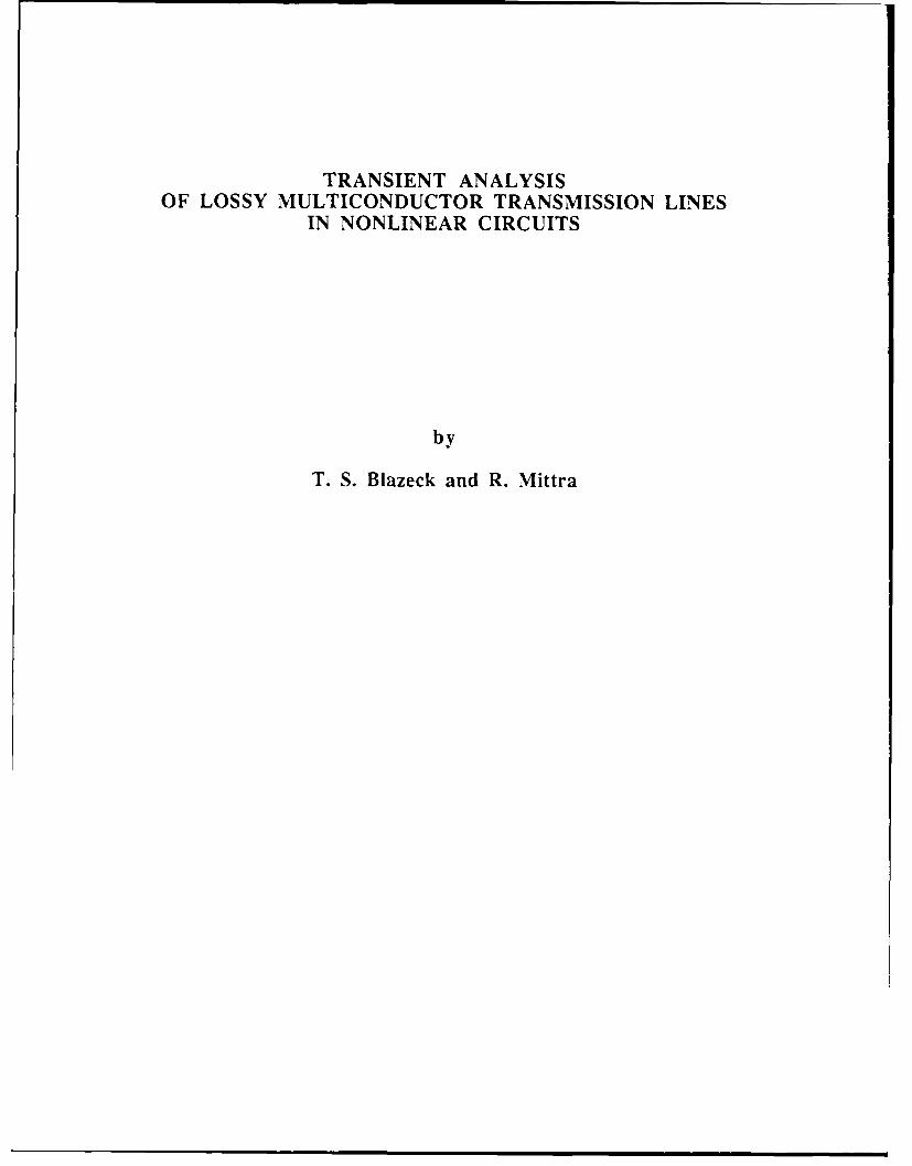
A linear capacitor is illustrated in Fig. 2.1 (a). The branch equations for the capaci-
tor are
qd= =i dq=Cv
dr
where C is the capacitance, v is the voltage across the capacitor, q is the charge on one of
its plates, and i is the current through the capacitor from node y to node z. Using the trap-
ezoidal method to discretize = i at time tk~1 results in
hqk+l = qk + '(ik + ik+)
Substituting Cv for q and solving for ik+1 yield
ik+1 = 2Cvk+i - CVk + i k (2.8)
As shown in Fig. 2. 1(b), Eq. (2.8) can be realized as a resistor with conductance 2C/h in
parallel with a current source of value 2Cvdh + ik. The conductance value is fixed because
the time step h is constant, but due to the memory inherent in this energy-storage element,
11
ik +I
+
V C k +1 hl2C Vk2C/h +i k
z zo
(a) (b)
y z
y ... 2-C -..2C vy k+ I2CVk+ih h h
z_< -C..2C.. vz k+ (C, kh h
A x b
(c)
y z
y +1 Vyk+1
Z Vz k+I -
branch ... ik+t 2V + iequation h h "+
A x b
(d)
Figure 2.1 Linear capacitor: (a) symbol and definitions, (b) companion model at timetk+1, (c) element stamp, (d) element stamp with branch current as a variable.

12
the current source depends on the previous capacitor voltage and current. This means that
the current source will have to be updated at each time step.
Following the rules of MNA, one can visualize writing KCL at nodes y and z to
arrive at the nonzero entries, shown in Fig. 2.1 (c), of the coefficient matrix A and source
vector b. Since the current through the capacitor is expressible as a function of the voltage
across it, it was not necessary to introduce the current as a variable when implementing
KCL. However, it is sometimes convenient to do so, particularly when the current is
desired as an output variable, or when it is needed for a current-controlled element. In such
cases KCL is written at each node with the current as the variable, and then the discretized
branch equation, Eq. (2.8), is appended to get the nonzero entries of A and b indicated in
Fig. 2.1(d).
An analogous procedure is used to derive the companion model for a linear inductor
and its corresponding element stamp. The necessary equations for the inductor depicted in
Fig. 2.2(a) are
q Li do = v
where L is the inductance, v is the voltage across the inductor, 0 is the flux linking the
inductor coils, and i is the current through the inductor from node y to node z. Following
steps identical to those just used for the capacitor, the discretized branch equation for the
inductor at time tk+I is easily found to be
Vk+I = -L'k+ t - (.Lik + Vk (2.9)
This equation leads to the companion model illustrated in Fig. 2.2(b). Since a voltage
source is contained in the model, the stamp for this element is derived by writing KCL at
each terminal of the element using the current through the inductor as the variable, and then
Eq. (2.9) is added to get the A and b entries shown in Fig. 2.2(c).

13
+k+1
i 2L1h+ V k -Ii
i k 2L/h +vk
z z
(a) (b)
y' '
y y+1
+1 Vy k+l
Z-1 Vz k+l -
branch +1 -1 -2L ik+ + Vkequation h h -- ik + Vk)
A x b
(c)
Figure 2.2 Linear inductor: (a) symbol and definitions, (b) companion model at time tk+I ,(c) element stamp.

14
2.3.2 Controlled sources and coupled elements
Controlled sources are easily included in computer-aided circuit analysis programs
that utilize the modified nodal approach. The current-controlled current source (CCCS) is
employed as an example here.
The symbol for the CCCS is illustrated in Fig. 2.3(a). The branch equation for this
element is i = a ia, where ia is the controlling current through some element a, and a is the
gain of the source. The CCCS is a memoryless element; consequently, its companion
model at any time step is just the source itself. This model is shown in Fig. 2.3(b) and the
corresponding element stamps are depicted in Figs. 2.3(c) and 2.3(d). When constructing
these stamps, the controlling current ia was assumed to be available as a circuit variable.
The stamps of other types of controlled sources are derived in much the same manner.
Coupled elements can generally be characterized by some combination of linear
resistors and controlled sources. Take for instance the coupled inductors illustrated in Fig.
2.4(a). The equations for this element can be written compactly in matrix form as
(p=Li d-- - v
where v is a vector of branch voltages, (p a vector of related fluxes, i a vector of branch
currents, and L the inductance matrix. Discretizing v = v at time tk+I, substituting Li for
(p, and solving for Vk+1 yield
Vk+I = -!Lik+l - (Lik + vk (2.10)
h k-ih
Expanding Eq. (2.10), the following is obtained:
V1 k+I = -L i k+I + -Mi2kl - " LIli k + -Mi 2 k + VI k) (2.11 a)
V2 k* Mi k-I + 2 2 k+ - (2. k+ Li VTMI1 2 2 i 2 k) (2.1 lb)
h h

15
+ + +1
V Vak +1v ai a la k +1
z z 0
(a) (b)
y "ia'"
-- ay ... +-a
a branch la k.lequation ... •
A x b
(c)
Figure 2.3 Linear current-controlled current source: (a) symbol and definitions, (b) com-panion model at time tk+1, (c) element stamp.

16.
Y22
M
V2 v LitL 22
z1
-2
(a)
+2 2 k4- Ik
2L, 1/h 2L22/h
V 2 k +1 V i k + + 2 k 1 M h+ i k 1 M h
+ 2/h(LI ji1 kc + Mi2 k) + 2/h(Mil k + L 22 i2 kc)
z1 0
Z2 3
(b)
Figure 2.4 Linear coupled inductors: (a) symbol and definitions, (b) companion model attime tk+t.

17
Y i z i Y 2 2 " .. i2 "
Y, ... +1
zI -1
Y2 +1
Z2 -1
+1 -1 2L 11 2Mbranch . h h
equations +1 -1 _2L/~ ~ ~ ~ ~ 2 +-1,._ML,..,.
h h
A
Vy, k+ 1
Vzt k+lI
Vy2 k+ 1
xVZ 2 k+ 1
ik"h(L klil + Mi 2 k) - VI k
i2 k+I - k(Mi I + L22i2 k) - V2kh
x b
(c)
Figure 2.4 (cont.) Linear coupled inductors: (c) element stamp.

18
From Eq. (2.11) one can see that the diagonal elements of L multiplied by 2/h are resis-
tance values, while the off-diagonal elements multiplied by 2/h are transresistance values of
gain for current-controlled voltage sources. The last terms on the right-hand sides of Eqs.
(2.1 La) and (2.1 lb) can be represented by independent voltage sources.
The companion model for the coupled inductors is shown in Fig. 2.4(b). The
stamp is constructed in a manner similar to that for a single inductor and is presented in
Fig. 2.4(c).
2.3.3 The nonlinear capacitor
Nonlinear resistors and capacitors are the nonlinear elements most needed when
modeling digital devices. Since the nonlinear capacitor actually contains a nonlinear resis-
tor in its companion model, the capacitor will be used as the demonstration element here.
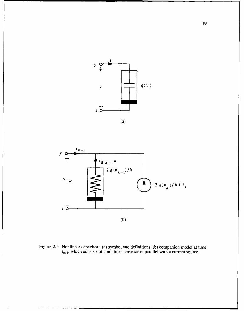
Figure 2.5(a) shows a nonlinear capacitor. Most nonlinear capacitors encountered
are voltage controlled and can be represented analytically by the following equations:
q = q(v) dqcit
where q, v, and i are charge, voltage, and current, respectively, and q(v) indicates that the
charge is some nonlinear function of the voltage. Discretizing the time derivative of the
charge using the trapezoidal rule and solving for ik+1 result in
ik+1 = 2 q vk+1) - ( 2 q(vk) + ikJ (2.12)
This equation can be represented by the equivalent circuit shown in Fig. 2.5(b). It is simi-
lar to the model for the linear capacitor of Fig. 2.1(b), except that now the resistor is non-
linear.
From Eq. (2.12) and Fig. 2.5(b), one can see that the current through the nonlinear
resistor obeys the equation iR = 2q(v)/h. A sample v-iR curve for this function has been
19
iyG-
+
vq(v)
z
(a)
ik +1y o 0
+iR k +1
2 q (v k +1)1h
v k+1 2 q(v k l h + i k
zo
(b)
Figure 2.5 Nonlinear capacitor: (a) symbol and definitions, (b) companion model at timetk+1, which consists of a nonlinear resistor in parallel with a current source.

20
drawn in Fig. 2.6(a). Suppose that the solution for the network had been found at time tk.
This result can be used to initiate an iteration scheme to find the solution at time tkI.After
the (j)th iteration, the solution for the nonlinear resistor will be a particular point on its v-iR
curve. Designating this point as PO on the sample curve of Fig. 2.6(a), the operation of
the resistor can be approximated by the line drawn tangent to the curve at that point. The
equation for this line is
U,, ) - .(j W j) U)(iR k+ = k+ k+ +S (2.13)
where
() 2 aq(v)v k+1
is the slope at point PU') and IS () is the 1R intercept. Solving Eq. (2.13) for this interceptSk+1
yields
I () W (j) (j) W JSk+I =- R k+1 - gk+lvc+l
Now substituting I') I back into Eq. (2.13), and updating the iteration count on the
unknown variables iR k+I and Vk+1, the following recursive formula is obtained:
(Q+1) = (j) (j+i) (j)iR k+I =gk 6vk+l + iS k+1 (2.14)
Equation (2.14) can be modeled by the parallel combination of resistor and current source
shown in Fig. 2.6(b). Substituting Eq. (2.14) into Eq. (2.12) yields (since iR = 2q(v)/h)
(j+l) (j) (s+i) () (2q( +) kq(v.15)Q+1 = +IS,1 -+ Is+ k (2.15)
Equation (2.15) leads to the overall companion model of Fig. 2.7(a) for the nonlinear
capacitor. This model characterizes the capacitor for iteration (j+l) at time tk+1. The

21
'R
'R 2q(v)Ih
(a)
(j +1)
iR P +)
+,~
; +1) k )
zO
(b)
Figure 2.6 Nonlinear resistor of Eq. (2.12) and Fig. 2.5(b): (a) sample v-iR curve,(o) companion model for iteration (j+l1) at time tr+.
=~~~~~~~~~~~ +a1ilIl •l i

22
(j +1)k I
y N+
(j+1) (j) (j) 2q(v )/h +iVk+1 (+1 is k +1k
z
(a)
y z
Uy() 2q(vk)/h + i1 - USk)
. igk+l Vyk+1 iS k1
- .1 . gk)+1 ... z kI - 2q(Vk)/h + ik
'"+ + k+1
A x b
(b)
y z
Vy k+ 1
-1 Vz k+l -
branch W -1 ik+I 2q(vk)/h + ik -equation "" ki -+l I S k+I
A x b
(c)
Figure 2.7 Nonlinear capacitor: (a) companion model for iteration (j+1) at time tk+ 1,
(b) element stamp, (c) element stamp with branch current as a variable.

23
linearization method presented here can be shown to be identical to the Newton-Raphson
method discussed in Section 2.2 [341.
Comparing the companion model for the nonlinear capacitor here with that of the
linear capacitor of Fig. 2.1(b), it can be seen that they have the same form. This being the
case, the element stamps for the nonlinear capacitor are easily constructed and are illustrated
in Figs. 2.7(b) and 2.7(c). When using the stamp of Fig. 2.7(b), convergence of the volt-
age within the prescribed limits does not always mean that sufficient convergence of the
current has occurred. For this reason, the stamp of Fig. 2.7(c) is generally preferred for
nonlinear elements since the current is available as a variable and may be subjected to the
same convergence requirements as the voltage.
2.4 Conclusions
In this chapter, a commonly used and completely general method of computer-aided
circuit analysis was presented. Implementation of a particular element in a circuit analysis
program consists of developing a companion model for that element and substituting the
element's stamp into the coefficient matrix A and source vector b. The overall solution of a
network amounts to solving a sequence of nonlinear resistive circuits by iterating a se-
quence of linear resistive circuits. In the following chapter, two different companion
models and their corresponding element stamps are developed for a lossy multiconductor
transmission line in order that it may be included in a circuit analysis program of the type
discussed in this chapter.

24
CHAPTER 3
LOSSY MULTICONDUCTOR TRANSMISSION LINES
3.1 Introduction
The analysis of nonlinear circuits, in the general case, can be performed only in the
time domain. On the other hand, the analysis of lossy transmission lines, particularly those
with frequency-dependent parameters, is handled most conveniently in the frequency
domain. Therefore, in order to devise a method of analysis for lossy multiconductor
transmission lines in nonlinear circuits, it is necessary to combine solutions from the two
domains. Assuming that the transmission lines are linear, the inverse Fourier transform
can be used to convert frequency-domain characterizations of the lines to the time domain.
Boundary conditions at the interface of the lossy distributed lines and lumped nonlinear
networks can then be matched at discrete time steps. [31 ]
In this chapter, the lossy multiconductor transmission line equations are first solved
in the frequency domain; then, the inverse Fourier transform is utilized to switch to the time
domain where two different companion models are developed to represent the multicon-
ductor line at its endpoints. One of the models consists of a discretized Thevenin equiva-
lent circuit for each end of the line, while the other model consists of discretized Norton
equivalent circuits. Depending on the properties of the line, it may be advantageous to use
one or the other. In addition, numerical issues are discussed for calculating and imple-
menting the models in a general circuit analysis program.
3.2 Frequency-Domain Solutions
A lossy (n+l)-conductor transmission I ne of .lGoth d i4 k hrwrin Fig. 3.1. The
telegrapher's equations for this transmission line can be expressed in matrix form as [35]

25
V1(x,:) (x,) i+
V2(x,t) :)2
1 (x 0
R, L, G, C
C reference I
x=0 x=d
Figure 3.1 Lossy (n+1)-conductor transmission line of length d.

26
avx,t) a (x,t)ax RI(x,t) + L- (3. 1a)
- = GV(x,t) + C------- (3.1 b)
where x and t are the spacial and temporal variables, respectively; V(xt) is an n x 1 vector
of line voltages; I(x,t) is an n x 1 vector of line currents; and R, L, G, and C are the n x n
per-unit-length resistance, inductance, conductance, and capacitance matrices, respectively.
The jth element of V(x,t), Vj(x,t), and the jth element of I(x,t), I(x,t), are the voltage and
current, respectively, on line j. In the formulation above, the line-parameter matrices are
constant; this is of limited usefulness since for even relatively slowly varying signals the
relationship betwecn voltage and current on most trinsmission systems is actually more
complicated [35]. Once Eq. (3.1) has been transformed into the frequency domain, this
restriction on the time rate of change of voltages and currents can be overcome in many
cases by allowing the line-parameter matrices R, L, G, and C to be frequency dependent.
Proceeding in this manner, the Fourier transform of Eq. (3.1) with respect to time t yields
V(x,ov)VX = (R + joL)I(x, )
3I(x, co)ax = (G +jcoC)V(x.a))
where o) is the radian frequency; then, explicitly showing the frequency dependence of the
line-parameter matrices leads to
V(x,cv) (.aa(x'C = [R(o) +jaL()]I(x,o) = Z(o)I(x,o)) (3.2a)
0l(x,acv)
x = [G(co) +jo)C(co)IV(x,o) = Y(ov)V(x,ov) (3.2b)
where the impedance per unit length, Z(co) = R(co) +jo)L(o)), and the admittance per unit
length, Y(o)) = G(o) +jo)C(o), have been introduced. As a consequence of reciprocity,

27
R(w), L(o), G(o)), and C(co) are symmetric; therefore, so are Z(wo) and Y(co). A physical
interpretation of R(co), L(a)), G(o)), and C(o) is given later in Sec. 3.2.1. The calculation
of these matrices is not a part of this work. In this study, for any simulation, values for
R(o), L(o), G(wo), and C(o) will be assumed to be available for each transmission line
encountered; they can be measured or calculated by one of the several available techniques
[36]-[41].
In order to characterize multiconductor systems by the line-parameter matrices, the
modes of propagation must be transverse electromagnetic (TEM) or quasi-TEM. In multi-
conductor transmission line systems with conductor losses, whether the systems are con-
structed with homogeneous or nonhomogeneous dielectrics, the existence of purely TEM
modes is nut possible; however, as long as the losses are small, quasi-TEM modes can
propagate. In fact, as long as the wavelength of the highest frequency under consideration
is long compared to the greatest cross-sectional distance of the system, only quasi-TEM
modes can propagate. In addition to these implicit constraints, it also will be assumed that
the line is of uniform cross section throughout its length; that is, R, L, G, and C are
assumed to be constant with respect to the spacial variable x.
Proceeding now to the solution of Eq. (3.2), substituting Eq. (3.2b) into the
derivative of Eq. (3.2a) and Eq. (3.2a) into the derivative of Eq. (3.2b) yields one equation
in terms of the line voltages and another in terms of the line currents:
a2Va2 = zYv = r2 V (3.3a)ax2
2
where the propagation matrix F has been introduced. In Eq. (3.3a), F2 = ZY has been
defined, and due to the symmetry of Z and Y, YZ then equals (F 2) as shown in Eq.
(3.3b). In general, even though Z and Y are symmetric, 1- 2 is not. If the existence of two

28
nonsingular square matrices E and J is assumed, then left-multiplying both sides of Eq.
(3.3a) by E-1 and both sides of Eq. (3.3b) by J results in
a2E-1V = E- 1F2EE-?V (3.4a)
a2~3x 2
a 3- I JI(F2)Tjj-1I (3.4b)
ax2
where the identity matrix has been inserted in the right-hand sides of Eqs. (3.4a) and (3.4b)
as EE-1 and JJ-l, respectively. The matrix products E- r E and J-(F )TJ in Eq. (3.4)
represent similarity transformations of r2 and (F2)T, respectively. If there exists n inde-
pendent eigenvectors of r2 and n independent eigenvectors of (r2)T, and the columns of E
and J are chosen, respectively, to be these eigenvectors, then the aforementioned similarity
transformations result in diagonal matrices. The existence of eigenvectors that diagonalize
r-2 and (F:)T will be assumed throughout this investigation. In fact, it is well known that a
matrix and its transpose are similar to the same diagonal matrix [42]; designating this matrix
as A2 yields
A2 = E-1F2E = j-(F2)Tj (3.5)
2 2 T7The diagonal elements of A ae the eigenvalues of F and (-2) . Their square roots are the
complex quasi-TEM propagation modes of the lossy multiconductor transmission line; for
this reason, A will be referred to as the modal propagation matrix. The jth columns of E
and J are the voltage and current eigenvectors, respectively, associated with thejth eigen-
2value of A . Now substituting Eq. (3.5) into Eq. (3.4) and defining the modal variables
Vm = E-iV and Im = J-1I lead to
a2V ,-V, (3.6a)
ax2

29
D2Im 2=AIm (3.6b)x2
The modal voltage equation, Eq. (3.6a), and the modal current equation, Eq. (3.6b), can be
solved independently of one another. First, the solution to the voltage equation will be
derived. Since A2 is diagonal, the individual equations in Eq. (3.6a) are decoupled. This
means, for instance, that modal voltage Vim, the jth element of Vm, depends only on the
derivative of Vj, and no other modal voltages; therefore, Eq. (3.6a) is actually n separate
scalar equations of the form
ax 2 = im
where Aj is the jth diagonal element of A and is the propagation constant for mode j. The
solution of this equation is
V =eYxV + + ekfVvjm = e m jm
where Vm + and Vjm- are scalar constants that depend on the boundary conditions. Conse-
quently, the solution of Eq. (3.6a) can be written in matrix form as
-AxV,,m=e -,m+e eAV, (3.7)
where e-A , the modal exponential propagation matrix, is a diagonal matrix whose jth
diagonal element is e-A7X, and Vm and Vm are vector constants. Multiplying each side of
Eq. (3.7) on the left by E and inserting the identity matrix as E-1E in each term on the
right-hand side result in
EVm = Ee-A E-1 EV +Ee A EV,,

30
Making use of a previous definition relating modal voltages and line voltages [V = EVm]
and the fact from matrix algebra that Ee-xE- 1 = e-EAE- [421 yields
V = e-EA- 1xv + + eEAE- 1xv -
where line-voltage constants V = EVm+ and V- = EVm- have been defined. Now utiliz-
ing the definition of A from Eq. (3.5), the solution for the voltage as a function of x is
obtained:
V = e-rXV+ + erXV - (3.8)
where e- rx, the exponential propagation matrix, has been introduced. The first term on the
right-hand side of Eq. (3.8) describes a vector of positive traveling waves, while the
second term represents a vector of negative traveling waves. To find the solution for the
current, Eq. (3.8) is substituted into Eq. (3.2a). Taking the derivative and rearranging
some terms lead to
Z01 = e-rXV + - e rxV - (3.9)
where
z 0 = r-Iz (3.10)
is called the characteristic impedance matrix. From Eqs. (3.8) and (3.9), it can be seen that
Z0 relates the positive and negative traveling voltage waves to the positive and negative
traveling current waves, respectively. As shown in Sec. 3.2.2, the characteristic
impedance matrix Z0 is symmetric. Equations (3.8) and (3.9) are the solution to the lossy
multiconductor transmission line equation, Eq. (3.2). Note that the solution has 2n inde-
pendent constants V+ and V- that depend on the boundary conditions.

31
A different form of the solution of Eq. (3.2) can be obtained by solving the modal
current equation, Eq. (3.6b). If this is done, the solutions for the current and voltage are
obtained as
T TI = e-r Xl+ - erXr (3.1 la)
T TYoV = e-r Xl+ + erx (3.1 lb)
where
YO = (F T)-Y (3.12)
is the characteristic admittance matrix and I" and 1 are constant vectors. The minus sign
preceding the second term in Eq. (3.1 la) arises from the fact that I- is defined as positive
in the opposite direction of I4*, which has the same reference direction as the total current I
(see Fig. 3.1). As might be expected, Y0 is the inverse of Z0 . This is shown to be the
case in Sec. 3.2.2. Note that this means that Y0 is also symmetric.
Equations (3.8), (3.9), (3.11a), and (3.1 lb) will be used in Sec. 3.3 to derive two
time-domain models for a lossy multiconductor transmission line. But first, in the next two
subsections, a discussion of the line-parameter matrices and several auxiliary proofs are
given.
3.2.1 Interpretation of the line-parameter matrices
A physical interpretation of R(co), L(w), G(w), and C(w) may be obtained by gen-
eralizing the definitions of their corresponding scalar-valued parameters. Referring to Fig.
3.1, say that linej has been charged to one volt (in the time-harmonic sense) with all other
lines held at a voltage of zero; then, Ci, the ijth entry of C, is equal to the charge per unit
length induced on line i. The off-diagonal elements of C, sometimes called electrostatic
inductance coefficients, are always negative. The diagonal entries, on the other hand, are
always positive and are the self-capacitances of the individual lines of the n-line system.

32
The conductance matrix G can be analyzed in a similar manner. Again, with linej charged
to one volt and all other lines at zero volts, the net current leaving line i per unit length is
entry Gii of G. As is the case with the capacitance entries, Gij < 0 for i *j, while Gj > O.
As one might expect, an entry in L, such as Lij, measures the flux per unit length linking
the loop formed by line i and the reference conductor due to a one-amp current flowing in
line ]. Of course, diagonal entries represent self-inductances while off-diagonal entries are
referred to as mutual inductances. Entry Rii of R measures the voltage drop along line i per
unit length due to a one-amp current flowing in line j. For i =j, this is simply the usual line
resistance. For i #j, it may seem impossible that current in a conductor can cause a voltage
drop in a conductor other than itself. Strictly speaking it cannot; however, just as the skin
effect of an isolated conductor can cause a redistribution of current that results in an effec-
tive increase in resistance of that conductor, the time-varying current in a line can also cause
a redistribution of current in a neighboring line. Therefore, the effective resistance of a
conductor in the neighborhood of other current-carrying conductors depends on those cur-
rents. This dependency is modeled by the off-diagonal elements of R.
3.2.2 Proof that Z0 = ZoT and Y0 = Z0- 1
That Zo is symmetric and its inverse equal to Y0 are commonly used facts; never-
theless, complete and efficient proofs are hard to find. For instance, the symmetry of Z0
has been argued based on reciprocity [4] even though such reasoning should be reserved
for fundamental physical relations such as the line-parameter matrices; other proofs have
been either incomplete [5] or, in the corresponding lossless-line case, inefficient [18].
First, it must be shown that the matrix product E-1 ZJ commutes with A- , that is,
E-IZJA -1 = A-1E-'ZJ (3.13)
The starting point is the definition of A2 from Eq. (3.5):
E- F2E = J- (F2) J = A

33
Substituting ZY for 1"2 and remembering that Z and Y are symmetric yield
E-1 ZYE = J-1YZJ = A2
Inserting the identity matrix as jj-1 into one definition of A2 and as EE-1 into the other
definition results in
E-1ZJJ-1YE = j-'YEE-1 ZJ = A2
Defining Az - E-1 ZJ and Ay = J-lYE, the preceding equation can be rewritten as
AzAy = AyA z = A2
Now, since Az and Ay commute with each other, they also commute with their product A2
and its inverse A-2. Also, since A-2 is diagonal, its square root A-' is diagonal.
Therefore, Az and Ay also commute with A-1, and Eq. (3.13) is proved.
To show that Zo = ZoT, one begins with Zo = r-Z [Eq. (3.10)]; then,
ZoT = (F"1z)T = Z(Fr)-l = ZJA-1j-l = EE- ZJA-lj-1
Using Eq. (3.13) yields the desired result:
Z0 =EA-IE-iZjj-1 = EA-1E-1Z = F-Z = Zo
Next, multiplying Zo = F-IZ by Y0 = (FT)-tY [Eq. (3.12)], one obtains
ZoY 0 = r - y = EA-IE-tZjA-tj-tY
Using Eq. (3.13) again leads to
ZoYO = EA-IA-IE-1ZJJ- 1Y = F- 2F 2 = 1
where 1 is the identity matrix, and so Yo = Zo-

34
3.3 Time-Domain Models
In this section, two time-domain models for a lossy multiconductor transmission
line are developed. One of these is based on Eqs. (3.8) and (3.9), the solution to the modal
voltage equation, and results in a discretized Thevenin equivalent circuit for each end of the
transmission line; the other is based on Eqs. (3.1 la) and (3.11 b), the solution to the modal
current equation, and leads to discretized Norton equivalent circuits. The Thevenin equiv-
alent model will be developed first. Both the space dependence and frequency/time depen-
dence of the equations will be needed; consequently, they will be shown explicitly in the
following derivation. Equations (3.8) and (3.9) are rewritten here for convenience:
V(x,co) = e-r(W0)xV+(o) + er(wi)xv-(w) (3.14a)
Z0(co)I(x,oj) = e-r(°w)xV+(a) - e r(a)xv-(C) (3.14b)
Defining V+(x,co) = e-r((a)xV+(o) and V-(x,ao) = er(wxV-(o) and evaluating these equa-
tions at x = 0 yield
V+(x,oj) = er(c))xV+(0o) (3.15a)
V-(x,o) = er(w)xV-(0, o) (3.15b)
Substituting Eq. (3.15) into Eq. (3.14) and evaluating the result at x = 0 lead to
V(0,Co) = V+(O,a) + V-(0,c0) (3.16a)
Z0 (o)I(0,w) = V+(0,0) - V-(0,ow) (3.16b)
From Eq.(3.15b), one notices that V-(O,o) can be expressed as V-(d,o))e r(a)a where d is
the length of the multiconductor line. If this expression is substituted into Eqs. (3.16a) and
(3.16b), then adding the respective sides of the two resulting equations and rearranging
terms yield

35
V(O,o) = 2e-r(w)dV-(d,wo) + Zo(o)I(Og) (3.17)
Equation (3.17) expresses the near-end (x = 0) voltage in terms of the near-end current, the
far-end (x = d) reflected voltages, and the transfer function matrices Zo(Co) and e -r ( a .
Similarly, starting with Eq. (3.14) evaluated at the far end:
V(do)) = e-r(o)dV+(0,o) + e (M)d V-(O,O)) (3.18a)
-Z0(o(d, o) = e-r(w)d V+(0,o) - er(W)dV-(0,O)) (3.18b)
an equation is obtained that expresses the voltage at the far end in terms of the far-end cur-
rents, the near-end reflected voltages, and the transfer function matrices:
V(d,co) = 2e-r(W)dV (0,o) + Zo(o)I(d,(o) (3.19)
Note that a negative sign appears on the left-hand side of Eq. (3.18b) where its seems there
should be none. In the original lossy multiconductor transmission line equations, Eq.
(3.2), the reference direction for the current was chosen in the positive x direction as
depicted in Fig. 3.1. For symmetry purposes, it is more convenient to choose the reference
direction for the current at each end of the line to be into the line. This necessitates the
introduction of the negative sign in Eq. (3.18b).
Before transforming Eqs. (3.17) and (3.19) to the time domain, a modification will
be made to the characteristic impedance matrix Z0 . In general, as o) approaches infinity,
Z0 (wo) approaches a real constant matrix; therefore, Z0 will be separated into the sum of
two terms as shown below:
Z0 (O) = Zo,(o) + Ro (3.20)
where RO is defined as the limit of Zo(w) as o goes to infinity:
R0= lim Z0(o) (3.21)
nullnuulmllUnil lmm unll nn Illl m i4 n u

36
Equations (3.20) and (3.21) can be taken to define the "shifted" characteristic impedance
matrix Zo0 (o). The time-domain Thevenin companion model for the lossy multiconductor
transmission line can now be constructed. Since Eqs. (3.17) and (3.19) have the same
form, it will be necessary to show a detailed derivation for only one end of the line.
Working with the far end, Eq. (3.20) is substituted into Eq. (3.19) to obtain
V(d,o) = 2e-r(W)d V+(Oo) + Z0s(o)I(d,o) + RoI(do) (3.22)
Switching to the time domain, the inverse Fourier transform of this equation is taken with
respect to o to arrive at
V(d,t) = 2H(d,t) * V+(0,t) + Z0s(t) * I(d,t) + R01(d,t) (3.23)
where the asterisk denotes convolution and
H(dt) = 9 - l {e-r(&) I
in which 9 denotes the Fourier transform with respect to t. Explicitly showing the convo-
lution integral evaluated at time t = tk leads to
V(d,tk) = 2j H(d,r)V+(O,tk-)d'r +jk Zos(r)I(d,tk-r)dr + RoI(d,tk) (3.24)
In the computer implementation of this equation, the integrals must be approximated by
finite sums. Rewriting Eq. (3.24) using finite sums results in
k-1 k-1
V(d,tk) = 2XH(d,t)V (O,tk-t+l)At + XZos(tt)I(d,tk-t+l)At + RoI(d,tk) (3.25)_=0 1=0
The vector V+(0,t1), 1=1,...,k, shown in the first term on the right-hand side of the above
equation consists of all of the reflected voltages that have been placed on the line at the near
end since the beginning of the simulation. In Eq. (3.24) H(d,r) and Z0s(r) are impulse

37
response matrices; this means, for instance, that H(d,tt), 1=0...,k-l, in Eq. (3.25) is a
pulse response matrix. This pulse response matrix takes the pulses V+(O,tt)At, 1=1,...,k,
that are placed on the line at x = 0 and propagates them down the line to the far end; there-
fore, the summation in the first term is just the positive-going voltage wave vector arriving
at x = d at time tk, that is, V+(d,tk). The second summation on the right-hand side of Eq.
(3.25) involves the product of the pulse response matrix Zos(t), 1=0...,k-l, and a vector
of past current pulses at the far end of the line. It results in a "past-history" voltage source
that represents, to a certain extent, the history at the boundary between the line and its
termination at the far end since the beginning of the simulation. This voltage source will be
designated Vh(d,to. Summarizing, the following variables have been defined:
k-I
V+(d,tk) = H(d,tl)V (O,tk-tI+b)At (3.26a)1=0
k-I
Vh(dtk) = I ZS(tI)I(dtk-tI+)At (3.26b)1=0
Substituting these variables into Eq. (3.25) leads to
V(d,tk) = 2V+(d,tk) + Vh(d,tk) + R0l(d,tk) (3.27)
This equation expresses the voltage at the far end at time t k in terms of the far-end currents,
the constant resistance matrix R0, and two known voltages; it is the time domain counter-
part of Eq. (3.19). A similar derivation leads to an equation for the. near end of the line.
This equation may be written as
V(O,tk) = 2 V-(O,tk) + Vh(O,tk) + ROI(0,tk) (3.28)
where
k-I
V-(Otk) = XH(d,tI)V-(d,tk-tl+l)At (3.29a)1=0

38
k-I
Vh(0,t k) =Y Zos(t)I(O,tk-t+l )At (3.29b)1_-0
A lumped-element companion model for the lossy multiconductor line can now be
developed from Eqs. (3.27) and (3.28). The first two terms of the right-hand side of each
equation can be represented by a voltage source, while the third term indicates that the cur-
rents at each end of the line pass through a system of coupled resistances. The value of the
voltage source is the open-circuit voltage at time tk that results from an incident wave. The
set of coupled resistances represented by the matrix R0 is the instantaneous resistance
looking back into an infinite lossy multiconductor transmission line. This justifies the use
of the term Thevenin companion model for the equivalent circuit illustrated in Fig. 3.2. In
this figure, the resistance matrices are shown in block-diagram form. These matrices can
be implemented in a manner identical to the resistance matrix encountered in Chapter 2 for
the discretized coupled inductors: the diagonal elements of the matrix can be modeled as
two-terminal resistors, and the off-diagonal elements as current-controlled voltage sources.
Since the model for the lossy multiconductor transmission line can be expressed as an
assemblage of lumped elements, it can be easily included in any circuit analysis program.
This has been a major goal of this research.
The element stamp for the far end of the line is shown in Fig. 3.3. Since the model
contains voltage sources in each line, the line currents are also introduced as variables via
the branch equations, Eq. (3.27). These currents are needed in any case because their
values must be saved so that they are available for convolution with Zos(t). The topology
of the stamp for the near end of the line is identical to that for the far end and, therefore, is
not shown.
A Norton companion model for the lossy multiconductor transmission line, con-
sisting of current sources in parallel with coupled conductances, can be derived starting

39
IPA) +Vh(O~tk)+Vlhjdtk)I dy1 0+ L"- Z,
+ +
2Vft-(O,tk) 2Vfl4(dtk)
ypt)+V hOtk Vhdt:
Fiur 3.2 Thv+ncmainmdla ie t o os (n1)codt trnmiso
l2(ine of legt d.d~k

40
Z 1 z2 z, 11t 4727 6I,1
zi +1
z2 +1
zn +1
+1 -Ro 11 -Ro 12 -Ro in
branch +1 -Ro 2 1 -Ro 22 -Ro 2,equations
+1 -Ro0 n -Ro2 -R0n
A
V1 (d,tk-)
V2(d,tk)
Vn(d,tk)
xl(d,tk) 2Vl+(dtk) + Vlh(d,tk)
12(d,tk) 2V2 (d,tk) + V2h(d,tk)
I(d,tk) 2Vn+(dtk) + Vnh(d,tk)
x b
Figure 3.3 Element stamp associated with the Thevenin companion model of Figure 3.2.This stamp is for the far end of the line only.

41
from Eqs. (3.1 la) and (3.1 lb). These are repeated here for convenience with the indepen-
dent variables explicitly shown:
I(x,o) = e-rT(o)xI+(O,wo) - err(o)x I-(O,o) (3.30a)
Yo(CO)V(x, o) = e-rT(o,)xj+(Owo) + e r(°o)xr"(O,w) (3.30b)
Following a development analogous to that conducted for the modal voltage equation, one
arrives at the following equations that describe the line-end currents as functions of the line-
end voltages, the reflected currents at the opposite end, and the transfer function matrices
Yo(o)) and e- r (o) rT "
I(0,co) = -2e-r(o))dr (d,o) + Yo(co)V(O,o.) (3.31 a)
I(d,wo) = -2e - r(o)) dI+(O,o) + Y0(co)V(d, o) (3.3 1b)
Transforming these to the time domain and discretizing them in a manner similar to the
development of the Thevenin companion model lead to
I(0,tk) = -2-(O,tk) + Ih(O,tk) + GoV(O,tk) (3.32a)
1(d,tk) = -2I+(d,tk) + Ih(d,tk) + GOV(d,tk) (3.32b)
where
Go = lir Yo(o.)
Yos()) = Yo(wo) - Go
k-I
I-(0,tk) = E HT(dtt)I-(dtk-t+l)At1=0
k-I
Ih(0,tk) = Y Yo(tl)V (Otk-tiI)At1=0

42
k-i
l+(dtk) = I HT(dtt)I+(Otk-tl+l)At/=0
k-I
Ih(d'tk) = Y0 s(t1)V(dtk-t+t)AtI=O
The companion model corresponding to Eqs. (3.32a) and (3.32b) is shown in Fig. 3.4,
and the corresponding elez-nt stamp for the far end of the line is given in Fig. 3.5. Again,
the topology of the stamp for the near end of the line is the same as that for the far end.
3.3.1 Interpretation of the impulse response matrices
It is interesting to consider the physical interpretation of the impulse response
matrices H(d,t) and Z0 (t) encountered in this section. Referring to Fig. 3.6, a doubly-infi-
nite (n+l)-conductor transmission line with a voltage source of value 23(t), where 6(t) is
the impulse function, is showr inserted into line j at x = 0. Upon application of the
impulse at t = 0, a voltage of value 6(t) is introduced on line j at x = 0 +, and one of value
-3(t) is introduced at x = 0-. The signal at x = 0+ will then propagate in the positive x
direction. From the solution to the multiconductor Lransmission line equations given by
Eq. (3.8), and making use of the causality condition and the inverse Fourier transform, the
value of the voltage at x = d is easily found to be
V(d,t) = H(d,t) * [0"" 0 ((t) 0'". 0] (3.33)
where the impulse occurs in the jth row of the vector. From Eq. (3.33) it is e-en that
Hij(d,t), the ijth entiy of H(dt), is the voltage at x = d of linc i in the circuit of Fig. 3.6.
Similarly., another doubly-infinite (n+l)-conductor transmission line is shown in
Fig. 37, this time with a current source of value 23(t) connected between linej and the
reference conductor at x = 0. Upon application of the impulse at t = 0, half the current will
travel in the positive x direction and the other half will flow in the negative x direction. The

43
YI 0 l~o~k) I(d,tk) V1- (d,
V1 (0, tk) 21hI) 1+dk ,(d,tk)
y2 v ( -j 12j(d,t) z
V2O~k)22(Ok)± 42(dtk) V(~k
*2 0 Z
+ +
Yn n
+ I +
Figure 3.4 Norton companion model at time tk for a lossy (n+ 1)-conductor transmissionline of length d.

44
ZI Z2 z, "11" "12 "i.n
Z1 ... +1
Z2 +1
Zn +1
Go 11 Go 1 2 Go1n -1
branch Go 2 1 Go 22 Go -1equations ...
Go nl Gon2 Go ,j -1
A
VI (d,tk)
V2(d,tk)
Vn(d,tk)
x-
I1 (d,tk) 2l,+(d,tk) - 11 h(d,tk)
12(d,tk) 21 2 (d,tk) - 12h(d,tk)
In(d rk) 2IJn(d,tk) - lh(d,tk)
x b
Figure 3.5 Element stamp associated with the Norton companion model of Figure 3.4.This stamp is for the far end of the line only.

45
Vi(dt) = H..(d t)
-O 28(t)l
,~Q I
I n1 R(o), L(wo), G(co), C(ct) ,
SI referenceI
x=O x=d
Figure 3.6 Physical interpretation of the impulse response H$d,).
1I
Vi(O,t) . Zoij(t)
, I
28(t)
nI
R(co), L(o), G(o)), C(co)
I reference iI
x=0 x-d
Figure 3.7 Physical interpretation of the impulse response Zo0 j(t).

46
current flowing in the positive direction will see an impedance equal to the characteristic
impedance of the line or Z0(o)). Therefore, in the time domain the voltage at x = 0 is
V(0,) = Z0t * [0"" 0 8(t) ... 01Q T (3.34)
where again the impulse occurs in the jth row of the vector. From Eq. (3.34) it is seen that
Zosj(t), the ijth entry of Z0(t), is the voltage at x = 0 of line i in the circuit of Fig. 3.7.
Since the multiconductor transmission lines in Figs. 3.6 and 3.7 are infinite in each
direction, no reflections will occur at any time. In a lossless system, the impulse response
is an impulse at t = 0 for each entry of Zo(r) and the sum of n impulses delayed in time for
each entry of H(d,t). In general, the delays are of different length. Since there are no
reflections in the responses, their durations are finite; if the lines had been terminated by an
impedance other than Z0 (o), the responses would exist for all time. In the case of lossy
lines, each impulse response will have a "tail" that is due to the distortion of the line. In
some sense, the length (in time) of this tail, until the value of the response is negligible, is a
measure of the severity of the distortion caused by the line. As with the lossless case, the
impulse responses will still be relatively short since no reflections occur. The shorter
impulse responses make it simpler to carry out the inverse Fourier transform and also
decrease the amount of past-history values that need to be stored. This is an inherent
advantage of the modeling method presented in this chapter.
3.4 Numerical Considerations
This section contains a discussion of what is involved numerically in calculating
and implementing the lossy multiconductor transmission line models in a general circuit
analysis program.

47
The actual calculation of the matrix functions e-r(01)d or e -r(a) rd and Zo(O) or Y0 (o)
is quite involved. The derivation from Eq. (3.7) to Eq. (3.8) yields the means of com-
puting e-r(w)d:
e-r(o)d = E(o)e-A(w)dE(o))-t
Since C (W)Td = [e-r(w)d]T , it need not be considered further. Recalling the definitions of
Zo(w) and Yo(cp) from Eqs. (3.10) and (3.12):
Zo(co) = (w)-I Z(.o) Yo(w) = [l"()rly(o))
then making use of Eq. (3.5) and some matrix algebra lead to
Z0 o(o) = E(o)A(w)-iE(o)-t Z(co)
Y0(w) =J A(co)- J(o))-'Y(O)
However, because Y0(o)T = Y0(o) and Y(Wco)T= Y(o),
Y0 (o) = Y(co)r(a) -1 = Y(o)E(o,)A(a)-lE()) -
Consequently, only the voltage eigenvectors need to be calculated no matter which trans-
mission line model is used. Before calculating the inverse transform of the variables above
by a fast Fourier transform, values must be computed at discrete frequencies. This is
complicated by the fact that, in general, the eigenvalues and eigenvectors of F(o)) are fre-
quency dependent. The numerical computation of the eigenvalues and eigenvectors of a
complex matrix is a difficult and time-consuming procedure; however, because they remain
constant throughout a simulation, the impulse responses need only be .,alculated once for
each lossy multiconductor transmission line of the circuit.
Because the transmission lines dealt with here are linear, the companion model for
the lossy (n+l)-conductor transmission line need only be updated at each time step of a

48
simulation and not at each Newton-Raphson iteration. The summations in Eqs. (3.26a),
(3.26b), (3.29a), and (3.29b) must be performed at each time step. Over the course of a
simulation, each summation constitutes one-half of a convolution integral being performed
in the time domain. These convolutions represent the most time-consuming operation of
the analysis technique described herein. However, newer computers that use vectorized
arithmetic units have the capability of performing multiplications in parallel. The convo-
lution as developed in this investigation is essentially a dot product which is a vectorizable
operation. Existing computers have the capability of speeding up this operation by a factor
of fifty. In the near future, a speedup of a full two orders of magnitude may be expected.
The calculation of the inverse Fourier transforms is the most difficult numerical
procedure involved in the formulation of the time-domain models. In general, each entry of
Zo(t) or Y0(t) contains an impulse and a discontinuity at t = 0. The impulse occurs because
Z0 (w) and Y0(w) approach constant nonzero matrices as o nears infinity. These impulses
can be extracted easily enough by shifting the frequency domain counterpart of these matri-
ces as was done in Sec. 3.3. A simple procedure can be used to remove the discontinuity
from the shifted response that remains. Since the impulse responses are real, it follows that
Zos*(wo) = Zos(-co), for example, where the asterisk as a superscript indicates complex
conjugate; then
2 Re{Zos(o)} = Zos(o) + Z0,* ()) = Z0s(0)) + Z0s(-o)
Now the inverse Fourier transform of Zos(-co) is Zos(-t); therefore, 2 Re{Z 0,(a)} and
Z0,(t) + Zo,(-t) form a Fourier transform pair. But Z0,(t) and Z0s(-t) do not overlap
because Z0s(t) is causal; as a result, Z0s(t) can be recovered by taking the positive-t portion
of the Z0s(t) + Z0s(-t) sum. The sum of these two terms is real and even; consequently,
the discontinuity at the origin has been eliminated. Similar reasoning applies to the com-
putation of Yos(t).

49
Special problems arise whenever R or G is zero. In many practical cases, a solu-
tion of sufficient accuracy may be obtained by taking G to be 0, the zero matrix. Upon
close examination of Eq. (3.10), it is seen that Z0 (w) will then be undefined (infinite)
whenever o = 0. However, Y0 (co) is the inverse of Z0 (co); consequently, YD(co) will be
equal to zero for o = 0. Therefore, it would seem to be advantageous to use the second
formulation of the time domain model, the one that results in the Norton companion model
of Fig. 3.4, whenever G is zero or chosen to be so. Likewise, whenever R is zero at
o = 0 and G is not, it is easier to use the companion model of Fig. 3.2. If R and G both
approach iilfinity as o goes to zero, then in real transmission lines, both Y0(CO) and Z0 (co)
are also zero and either method may be used.
The inverse transform of the exponential propagation matrix e- r (w)d is slightly more
difficult to calculate than that of the impedance or admittance matrix. Imbedded in each
element of the exponential matrix are n delays that correspond to the n propagation modes
of an n-line system. As the frequency nears infinity, the real part of each entry of er(a))d
approaches a sum of n sinusoids. As was mentioned in Sec. 3.3. 1, this means that H(d,t)
contains a sum of n impulse functions delayed in time by the amount that it takes the corre-
sponding lossless modes to propagate from one end of the line to the other end. Once the
modal exponential propagation matrix e- A(w)d has been recombined to the full-matrix form,
there is no simple procedure to extract these impulse functions as was done for Y0(w) and
Z0 (co). In Y0(CO) and Zo(co), these impulse functions all occur at t = 0 in both the modal
and full-matrix forms. The effect is that e- ' ( " )d goes to a periodic function as Co approaches
infinity. Numerically, the inverse fast Fourier transform must be of finite length; conse-
quently, e-r~' 1) must be multiplied by some window function before the transform can be
calculated. A number of window functions are available for this purpose. Among these
are the rectangular, triangular, von Hann, and Hamming windows. It was found that the
Hamming window provided the best results. The Hamming window w(co) is shown here
to be

50
w(Co) = 0.54 + 0.46 cos (oA) -7r(At) < o < r/(At)
w(W) = 0 otherwise
Therefore, H(dt) is calculated as
H(d,t)=0 t <0
H(d,t) = -1{2 Re{e-r (l))}w(Co)} t _ 0
where the real-and-even scheme discussed earlier in the calculation of Zo,(t) is also used
above. The windowing results in a minor spreading of the final results that are nearly
imperceptible.
Each single or multiconductor transmission line represents an inherent delay in the
propagation of a signal or signals during a transient simulation. This can be seen in the
impulse response matrix H(d,t). Because of this propagation delay, the value of H(d,0) is
always equal to the zero mnatrix for any transmission line whether it is lossless or lossy.
This means that during any transient simulation, lumped-element networks separated by
transmission lines are effectively decoupled; that is, they do not depend upon one another.
Consequently, the coefficient matrix A can always be reordered into a block diagonal form,
and each block solved separately for each iteration of each time step. If the Thevenin
companion model of Fig. 3.2 is used, for example, each half of the equivalent circuit can
be considered a part of the lumped network to which it is connected. For large networks, a
significant savings of computer time may result since the number of multiplications re-
quired to solve a system of linear equations varies as the cube of the order of the system.
(If sparse matrix techniques are used, the number of multiplications for typical electrical
networks still varies at an exponential rate of approximately 1.5.) In the typical circuit
analysis program, the user must number the nodes consecutively starting from one with the
reference node being zero. In order to ease the implementation of this technique in the
program written for this thesis, the user must indicate the number of lumped element

51
networks involved in the simulation, number the nodes in each of these networks consecu-
tively, and indicate the largest node value for each lumped-element network.
3.5 Conclusions
In the time-domain analysis of nonlinear circuits, lossy multiconductor transmission
lines can be represented at each time step by discretized Thevenin equivalent circuits or
discretized Norton equivalent circuits. These models contain only lumped elements so they
can be easily implemented in a general circuit analysis program. The major obstacles
appear to be numerical in nature, but they do not seem to be severe enough to alter the
viability of the technique presented.

52
CHAPTER 4
RESULTS AND ANALYSIS
4.1 Introduction
In order to verify the analytical and numerical techniques developed in Chapter 3, a
computer program compatible with the circuit analysis method of Chapter 2 was written
incorporating the lossy multiconductor transmission line models [43]. It is an extension of
an earlier program written to include lossless multiconductor transmission lines [44]. The
new program can be used for the transient analysis of nonlinear circuits containing any
number of lossy frequency-dependent multiconductor transmission lines. It can also
handle coupled inductors and coupled capacitors of any order, as well as junction diodes
and bipolar transistors. As discussed in Chapter 2, the program uses modified nodal anal-
ysis to formulate the circuit equations, the trapezoidal algorithm (with a fixed time step) for
discrete integration, and the Newton-Raphson algorithm to iteratively solve systems of
nonlinear equations. In this chapter, the program is demonstrated for several circuit con-
figurations.
4.2 Simulation Examr'*s
The first example consists of a single transmission line (with ground return) termi-
nated by TI 74S04 (Schottky "ITL) inverters. As shown in Fig. 4.1, one inverter is used
as the driver of the line, and a fan-out of three inverters is used to terminate the line. The
transmission line is 10.0 in. (0.254 m) long with an inductance L of 307.1 nH/m and a
capacitance C of 85.3 pF/m. The frequency-dependent skin effect was modeled by a
resistance R = max(6.8,0.26'I7/10 3) 0/in. = max{267.7, 10.244-f/103) Q/m wheref is
the frequency in Hertz. The conductance G of the dielectric was assumed to be negligible.

53
1 22 40time (ns)
Figure 4.1 Single lossy transmission line interconnecting TI 74S04 inverters. The output
of the driver D is made to switch from low to high at 1 ns and then from high
to low at 22 ns. For the inverters: rise time = 2.2 ns, fall time = 2.2 ns, Cin =5.4 pF, Cout = 5.0 pF. For the transmission line: R = max(6.8, 0.26 fj/103}D/in. = max(267.7, 10.24'f /1O3} Q/m, L = 307.1 ni/m, G = 0.0 S/m, andC = 85.3 pF/m. When losses are neglected the characteristic impedance is 60 Q.

54
These parameters are those of a high-density interconnect used to transmit data in fast
computers [45].
For computational efficiency, a simplified model [46] was used to represent the
digital devices. When the inverter is used as a load, its input is modeled as a parallel
combination of a constant capacitance and a voltage-dependent nonlinear resistor as shown
in Fig. 4.2(a). When the inverter is used as a driver, its output is modeled in a manner
similar to that of its input, except that now the nonlinear resistor is time varying. This
nh el is shown in Fig. 4.2(b). As an example, the v-i curves of the nonlinear resistors
used for the TI 74S04 inverter are shown in Fig. 4.3. The input curve is shown in Fig.
4.3(a), ard the output curves are shown in Fig. 4.3(b). The input curve, output-low
curie, and output-high curve are generated from static measurements [47]. The transition
curves between the two output curves are generated by the program.
When the driver is initially triggered by the pulse (see Fig. 4.1), the device is oper-
ating on the output-low curve of Fig. 4.3(b). During a period corresponding to the rise
time of the inverter, the model passes through the transition curves to the output-high curve
where it remains as long as the input to the driver is held low. When the input to the
inverter is switched back to high, the output switches back to the low state via the same
transition curves during the fall time specified for the device. A number of researchers
have had good experimental agreement using a model of this type [401,[46].
The computer simulation of the circuit of Fig. 4.1 was first conducted using the
methods developed in Chapter 3 to model the transmission line and then using the lumped
delay elements of Fig. 4.4 to model the line. Ten lumped delay elements were used to
approximate the line; the low-frequency resistance was used since frequency dependence
cannot be modeled by the delay elements. A comparison of the resulting waveforms is
shown in Fig. 4.5. In Fig. 4.5(a) the two simulations are compared at the drive end, and
in Fig. 4.5(b) they are compared at the load end. Except for a small difference in the
steady-state values for the output-high state of the driver, the results are nearly identical.

55
0 1R in
(a)
+
0-
(b)
Figure 4.2 Inverter circuit model: (a) for the input when used as a load, (b) for the outputwhen used as a driver.

56
Inverter Input v-i Curve
125
75
' 25
-25
-75 . " . . p-2 0 2 4 6 8
Voltage (V)
(a)
Inverter Output v-i Curves
125
Output Low75 Transition Curves
S25-
.25 Output High
-75 , , ,-2 0 2 4 6 8
Voltage (V)
(b)
Figure 4.3 TI 74S04 inverter v-i curves.

57
6.8 ! 7.8 nH
2.167 pF
Figure 4.4 Lumped delay element: one of ten cascaded to model the lossy transmissionline of Fig. 4.1.
An RC effect in the rise and fall times that results from the conductor losses can be seen in
the figures. This is a major problem facing users of fast digital chips.
The next example consists of the lossless lines terminated by linear resistors and
capacitors as depicted in Fig. 4.6(a). The inductance and capacitance matrices and resulting
characteristic impedance matrix for the coupled lossless lines are shown in Fig. 4.6(b).
Even though the primary goal of this thesis has been to compute the transient responses of
lossy transmission lines with nonlinear terminations, this example can serve as a test for the
program since the results will be compared to a Laplace transform solution and an experi-
mental solution r32]. The solution obtained when the method of Chapter 3 is employed is
shown in Fig. 4.7(a); the solution by the method of Laplace transforms is shown in Fig.
4.7(b); and the experimental results are shown in Fig. 4.7(c). The two numerical solutions
are nearly identical as one would expect. The experimental solutions agree within sufficient
accuracy.
The literature is sparse concerning experiments that consist of pulse responses to
lossy multiconductor transmission lines. However, the article by Gruodis and Chang [301
contains such an experiment, and the next example compares simulated results using the
methods developed in this investigation to their experimental results. The circuit used for

58
Drive End4- A
3-
, 2
0 10 20 30 40
time (ns)
Load EndA
B!
3
J2-
I
00 10 20 30 40
time (ns)
Figure 4.5 Comparison between simulated waveforms for the circuit of Fig. 4.1 when thetransmission line is modeled by the method of Chapter 3 with a frequency-dependent resistance (curves A) and when it is modeled by lumped delayelements of the type in Fig. 4.4 (ect-,"ves B)

59
500) ). 14 in. =
~Signal Line
-_--~~5 2 p516 5F
2 3 time (ns) 1 6 5
Sense Line
50 Q 50 pF
(a)
f55 147 99 -22] [9.4 19.0]
L= _ 4 nH/m C=pF/m 0 =147 455_ 99 119.0 69.4]
(b)
Figure 4.6 Coupled lossless transmission line with linear terminations for numerical sim-ulations and experimental measurement: (a) circuit configuration, (b) induc-tance and capacitance matrices and resulting characteristic impedance matrix.

60
Signal Line at Drive End 0.8 Sense Line at Drive End
0.63--%0.4
2- 20.2
0 0
" 0.20"-0.4
- I -0.6 • , ' • , I I "0 10 20 30 40 0 10 20 30 40
time (ns) time (ns)
Signal Line at Drive End Sense Line at Drive End0.8-
3- 0.6-
S0.4
S0.2
C40.0.
-0.2
0-0.4
-I- . -0.6-
10 20 30 40 0 10 20 30 40time (ns) time (ns)
*imniruiiiuiuniimn
*EEEERh
Figure 4.7 Comparison among two types of simulated waveforms and experir.entalwaveforms for the circuit of Fig. 4.6: top, waveforms simulated by themethod of Chapter 3; middle, waveforms simulated by the Laplace transformmethod; bottom, experimental waveforms. For the experimental waveforms,the attenuation is a factor of 40 for the signal line and 10 for the sense line.

61
the experimental setup is shown in Fig. 4.8. Gruodis and Chang confined their experiment
to low frequencies (around 1 MHz) in order to minimize the effects of discontinuities in-
herent in connecting the line to the signal generator and terminating resistors. The trans-
mission line made use of a commercial telecommunication cable consisting of four #22-
AWG conductors. One wire of one of the two twisted pairs of which the cable consisted
was used as the signal line. The other wire of the same twisted pair was used as the sense
line. The second twisted pair along with the aluminum-coated mylar wrapping and braided
shield formed the ground return. The measured parameters of the transmission line are
shown in Table 4.1. The experimental results are given in Fig. 4.9(a) and the simulated
results are given in Fig. 4.9(b). As can easily be seen, all waveforms are very nearly
identical except for the load end of the signal line in which the simulated results do not
experience the slight rise-time degradation that occurs in the experimental case. However,
the results are well within acceptable limits of accuracy.
Note that for this simple example of two symmetrical lines, the eigenvector matrix
E turns out to be independent of frequency:
E--[1-1]
consisting of only the common and differential modes. The method described herein is not
limited to this case, and a more general case is considered in the final example.
Of important concern in the transmission of high-speed pulse signals is the effect of
discontinuities in the multiconductor lines used to interconnect digital circuits. In Fig. 4.10
a set of FAIR 74F04 (Advanced Schottky TI'L) inverters is shown interconnected by two
(4+1)-conductor transmission lines joined by a connector. Figure 4.11 shows the micro-
strip used for the multiconductor transmission lines along with its inductance L and capac-
itance C matrices. The L and C matrices were calculated by the method of Chan and Mittra
[41]. The microstrip dielectric had a relative permittivity er of 4.5. The relative width of

62
50 Q2 1' 123 m --
PULSEI50k
, I
0.3 0.8 4.1 4.6 6.5time (pIs)
Sense Line
50 50
Figure 4.8 Coupled lossy transmission line with linear terminations. A telecommunicationcable consisting of four #22-AWG conductors in two twisted pairs is used forthe transmission line. The signal line consists of one wire of one of the twistedpairs, and the sense line consists of the other wire of the same twisted pair.The second twisted pair along with the aluminum-coated mylar wrapping andbraided shield form the ground return. The measured parameters of the trans-mission line are shown in Table 4. 1.

63
Table 4.1 Coupled transmission line parameters [30].
Resistance (fl/km)Freq. (kHz) RI, R12 R22
0.0 64.06 12.83 64.062.0 64.01 12.19 64.015.0 63.93 12.26 63.93
10.0 64.90 12.45 64.9020.0 68.29 13.25 68.2950.0 77.93 17.36 77.93
100.0 101.47 23.59 101.47200.0 125.72 26.09 125.72
Inductance (H/km)
Freq. (kHz) LI L12 L2
0.0 510.5 99.5 510.52.C 510.5 99.5 510.55.0 498.0 98.3 498.0
10.0 492.0 96.4 492.020.0 477.7 94.3 477.750.0 451.1 81.8 451.1
100.0 435.4 81.8 435.4200.0 402.2 68.8 402.2500.0 360.1 58.8 360.1
1000.0 340.9 58.0 340.9
Conductance (S/km)Freq. (Wz) GI G12 G22
all 0.0 0.0 0.0
Capacitance (nF/krm)Freq. (kHz) C11 C12
0.0 86.2 -14.0 86.22.0 74.0 -12.1 74.05.0 74.5 -12.7 74.5
10.0 75.0 -14.1 75.020.0 75.2 -15.9 75.250.0 75.6 -14.0 75.6
100.0 75.4 -15.3 75.4200.0 76.8 -14.7 76.8500.0 76.8 -14.2 76.8
1000.0 76.6 -14.6 76.6

64
Experimental Waveforms
A
1.0
U
o I 2 3 ,46
Simulated Waveforms1.6"
1.4"
OA A
1.2
>c
1.0-
S 0.8-
0.6-
" 0.4-
0.2-
0.0 " D
-0.2--0.4
0 1 2 3 4 5 6
time (microseconds)
Figure 4.9 Experimental [30] and simulated waveforms for the circuit of Fig. 4.8. CurveA, one-half of drive signal; curve B, drive end of signal line; curve C, l"-d endof signal line; curve D, drive end of sense line; curve E, load end of sense line.

65
l~1 in. 13 o in. i~
pC
D N_
5 V All digital devices are FAIR 74F04 inverters
PULSE
1 30 60time (ns)
Figure 4.10 Multiconductor transmission lines joined by a connector and terminated byFAIR 74F04 inverters. The output of the driver D is made to switch fromlow to high at 1 ns and then from high to low at 30 ns. For the inverters: risetime = 2.75 ns, fall time = 1.25 ns, Cin = 4.6 pF, Cu t = 5.0 pF. The geom-etry of the multiconductor lines is depicted in Fig. 4.11 along with their L andC matrices. When the lines are lossy, R = 50 x I 92/m, where 1 is the iden-tity matrix, and G = 0 S/m. The L, and C, matrices for the connector aregiven in Fig. 4.12.

66
0 Dimensions indicated are relative
I !::::iii:% ::::i~iii!:i~i::iiiii! '':ii~ii~I ............
(a)
422.1 75.8 25.3 11.9 85.85 -8.55 -0.64 -0.28
75.8 420.1 75.4 25.3 -8.55 86.96 -8.48 -0.64L= nH/m C= pF/m
25.3 75.4 420.1 75.8 -0.64 -8.48 86.96 -8.55
11.8 25.3 75.8 422.1 -0.28 -0.64 -8.55 85.85
(b)
70.41 9.84 2.67 1.14
9.84 70.08 9.77 2.67= 2.67 9.77 70.08 9.84
1.14 2.67 9.84 70.41
(c)
Figure 4.11 Microstrip used for the multiconductor transmission lines in the circuit of Fig.4.10: (a) cross section, (b) inductance and capacitance matrices, (c) charac-teristic impedance matrix when the microstrip is lossless.

67
27.3 16.4 15.0 16.2 1582 -736 -154 -520
16.4 27.1 16.1 12.0 -736 1536 -727 -160Lc =nH Cc = flF
15.0 16.1 27.3 15.9 -154 -727 1516 -349
16.2 12.0 15.9 27.9 -520 -160 -349 1589
Figure 4.12 Inductance and capacitance matrices for the connector in the circuit of Fig. 4.10.
the conductors, spacing between the conductors, and the depth of the dielectric were taken
to be one. When the lines were lossy, a diagonal resistance matrix with non-zero va!, cs of
53 f./m was chosen. The conductance of the dielectric was neglected. This is a reasonable
assumption for the frequency range (up to a few gigahertz) of digital signal transmission.
The connector was modeled by a 7t-equivalent circuit with inductance L c and capacitance
CC matrices as shown in Fig. 4.12. (The capacitance matrix was split between the two
halves of the it-equivalent circuit.)
Figure 4.13 shows a comparison between simulated waveforms for the signal line
of the circuit of Fig. 4.10 when the transmission lines are lossless and when they are lossy;
Fig. 4.14 shows the same for the sense line indicated in Fig. 4.10. In general, the losses
caused significant attenuation and smoothing in both the signal and sense lines, but only a
minor reduction of rise and fall times. Although not obvious from these plots, the effect of
the connector is the small extra delay in the propagation time of the signal. This should not
be surprising since the model for it is a lumped delay element, albeit one that includes cou-
pled elements.
4.3 Conclusions
A number of simulation examples were presented to exercise the lousy multicon-
ductor transmission line model in circuits that contain linear and nonlinear elements. The

68
Signal Line at Drive End5-
4
S 3-2 lossless
S 2-lossy
0
0 10 20 30 40 50 60
time (ns)
Signal Line at Load End
54-
3-
2 lossless21
lossy
0-4;,. 1
0 10 20 30 40 50 60
time (ns)
Figure 4.13 Comparison between simulated waveforms for the signal line of the circuit ofFig. 4.10 when the transmission lines are lossless and when they are lossy.

69
Sense Line at Drive End1.5
1.0
0.5. lossless
0.0 - lossy
-0.5
0 10 20 30 40 50 60
time (ns)
Sense Line at Load End1.5"
1.0
_ 0.5- lossless
0.0 lossy
-0.5
-1.00 10 20 30 40 50 60
time (ns)
Figure 4.14 Comparison between simulated waveforms for the sense line of the circuit ofFig. 4.10 when the transmission lines are lossless and when they are lossy.

70
examples highlighted the interconnection of high-speed digital circuits by lossy multicon-
ductor transmission lines with and without discontinuities. Simulation results showed
good agreement with experimental results for both lossless and lossy multiconductor
transmission lines.

71
CHAPTER 5
CONCLUSIONS
Using the frequency-dependent transmission line parameters, two time-domain
models were developed for lossy multiconductor transmissions lines. It was shown that
the endpoints of a lossy multiconductor line could be represented at each time step by dis-
cretized Thevenin or Norton equivalent circuits. Because these models contain only
lumped elements, they can be easily implemented in a general circuit analysis program for
simulating the transient responses of nonlinear circuits. A number of transient simulations
were conducted in order to test the viability of the program. The program was found to
give good results and to be of a very general nature.
Of particular interest was the interconnection of high-speed digital circuits by lossy
multiconductor transmission lines containing discontinuities. The technique was demon-
strated for the most general case of lossy multiconductor transmission lines with nonlinear
terminations in which the modal transformation matrices were necessarily frequency
dependent. This case has been avoided very adroitly in the literature. Results have only
been shown for the simplest case of two symmetric conductors over a ground plane [30]-
[32]. In this particular case, the modal transformation matrices result in an even and odd
mode no matter what the frequency; therefore, the most general case is avoided. Also, the
capability of incorporating discontinuities into the transmission line structure was presented
for the first time.
A unique feature of the analysis procedure developed in this study was the exclu-
sive use of infinite-line impulse responses in the formulation of the time-domain models.
Because infinite lines are matched, there were no reflections in the impulse responses. The
result is that these impulse responses are necessarily shorter than those for the quasi-
matched case, such as the modified short-circuit parameters of Djordjevic et al. [311 and the

72
scattering parameters of Schutt-Aine [32]. Shorter impulse responses reduce the problem
of aliasing encountered when taking the inverse transform and decrease the amount of
computation that needs to be performed in the time domain. Techniques were presented to
facilitate the implementation of the fast Fourier transform which is utilized to convert
frequency-domain transfer functions to time-domain impulse responses.
The most serious drawback of the proposed technique is that direct integration of
the convolution integrals is carried out in the time domain. Since the number of multiplica-
2tions that must be performed is of the order of N , where N is the number of steps in the
simulation, this is indeed a very serious consideration. However, newer computers that
use vectorized arithmetic units have the capability of performing multiplications in parallel.
The convolution as developed in this investigation is essentially a dot product which is a
vectorizable operation. Existing computers have the capability of speeding up this opera-
tion by a factor of fifty. In the near future, a speedup of a full two orders of magnitude can
be expected.
There appears to be two possible solutions to the problem mentioned above. In the
first of these, the impulse responses are approximated by sums of exponentials; then, the
convolutions can be accomplished recursively. In the second, the transfer functions are
approximated by rational polynomials directly in the frequency domain so that state-variable
techniques may be used. In both of these methods, the amount of computation reeded to
calculate the convolutions is greatly reduced and the need to store past-history values of
voltage and current eliminated. The second procedure has been attempted by Gruodis and
Chang [301 in a method similar to the one presented herein. They use the diagonal form of
the exponential propagation matrix. The delays are extracted from the exponential func-
tions, and modal signals are propagated along the transmission line by shifting them at each
time step as is standard for lossless-line simulations. The waves are then shaped at the
opposite end of the line by the remaining portions of the propagation functions. However,
in converting between modal variables and line variables, they neglect the fact that the

73
transformation matrices are frequency-dependent. A physical interpretation of these trans-
formation functions is not possible; consequently, their approximation is necessarily more
difficult since they may be noncausal.
The inclusion of the lossy multiconductor transmission line models into an existing
circuit simulator such as SPICE is the most obvious future need. Current computer-aided
design tools for nonlinear circuits have the ability to model single lossless lines or use RC
ladders to model single resistive lines. They cannot accurately portray the multiline cou-
pling and frequency-dependent losses that arise when high-speed signals propagate
between digital circuits. The method presented in this study is currently limited to uniform
transmission lines. Tapered lines are also used by the computer and telecommunication
industries; as a result, the inclusion of nonuniform lines is also of importance. In addition,
the inclusion of nonlinear lines may be needed eventually, but a totally new procedure
would have to be devised since the Fourier transform could no longer be used. This will
probably not be necessary for digital circuit interconnections in the near future.

74
REFERENCES
[1] J. R. Carson and R. S. Hoyt, "Propagation of periodic currents over a system ofparallel wires," Bell Syst. Tech. J., vol. 6, pp. 495-545, July 1927.
[2] L. V. Bewley, Traveling Waves on Transmission Systems. New York: John Wileyand Sons, 1933.
[3] L. A. Pipes, "Matrix theory of multiconductor transmission lines," Phil. Mag., ser.7, vol. 24, pp. 97-113, July 1937.
[4] S. 0. Rice, "Steady state solutions of transmission line equations," Bell Syst. Tech.J., vol. 20, pp. 131-178, April 1941.
[5] L. M. Wedepohl, "Application of matrix methods to the solution of travelling-wavephenomena in polyphase systems," Proc. Inst. Electr. Eng., vol. 110, pp. 2200-2212, December 1963.
[6] J. R. Carson, "Wave propagation over parallel wires: the proximity effect," Phil.Mag., ser. 6, vol. 41, pp. 607-633, April 1921.
[7] J. R. Carson, "Wave propagation in overhead wires with ground return," Bell Syst.Tech. J., vol. 5, pp. 539-554, October 1926.
[8] J. P. Bickford and P. S. Doepel, "Calculation of switching transients with particularreference to line energisation," Proc. Inst. Electr. Eng., vol. 114, pp. 465-477, April1967.
[9] M. J. Battisson, S. J. Day, N. Mullineux, K. C. Parton, and J. R. Reed, "Calcula-tion of switching phenomena in power systems," Proc. Inst. Electr. Eng., vol. 114,pp. 478-486, April 1967.
[10] L. M. Wedepohl and S. E. T. Mohamed, "Multiconductor transmission lines-theoryof natural modes and Fourier integral applied to transient analysis," Proc. Inst. Electr.Eng., vol. 116, pp. 1553-1563, September 1969.
[111 D. B. Jarvis, "The effects of interconnections on high-speed logic circuits," IEEETrans. Electron. Comput., vol. EC-12, pp. 476-487, October 1963.
[12] A. Feller, H. R. Kaupp and J. J. Digiacomo, "Crosstalk and reflections in high-speed digital systems," AFIPS Conf. Proc., vol. 27, part 1, 1965 Fall Joint Com-puter Conf., pp. 511-525, 1965.
[131 1. Catt, "Crosstalk (noise) in digital systems," IEEE Trans. Electron. Comput., vol.EC-16, pp. 743-763, December 1967.
[141 J. A. DeFalco, "Reflection and crosstalk in logic circuit interconnections," IEEESpectrum, vol. 7, pp. 44-50, July 1970.
[15] H. Amemiya, "Time-domain analysis of multiple parallel transmission lines," RCARev., vol. 28, pp. 241-276, June 1967.

75
[16] H. W. Dommel, "Digital computer solution of electromagnetic transients in single-and multiphase networks," IEEE Trans. Power Apparatus Syst., vol. PAS-88, pp.388-399, April 1969.
[17] F.-Y. Chang, "Transient analysis of lossless coupled transmission lines in a nonho-mogeneous dielectric medium," IEEE Trans. Microwave Theory Tech., vol. MTh''-18, pp. 616-626, September 1970.
[18] C. W. Ho, "Theory and computer-aided analysis of lossless transmission lines,"IBM J. Res. Dev., vol. 17, pp. 249-255, May 1973.
[191 K. D. Marx, "Propagation modes, equivalent circuits, and characteristic terminationsfor multiconductor transmission lines with inhomogeneous dielectrics," IEEE Trans.Microwave Theory Tech., vol. MTT-21, pp. 450-457, July 1973.
[20] V. K. Tripathi and J. B Rettig, "A SPICE model for multiple coupled microstrips andother transmission lines," IEEE Trans. Microwave Theory Tech., vol. MTT-33, pp.1513-1518, December 1985.
[211 M. Silverberg and 0. Wing, "Time domain computer solutions for networks con-taining lumped nonlinear elements," IEEE Trans. Circuit Theory, vol. CT-15, pp.292-294, September 1968.
[22] A. Budner, "Introduction of frequency-dependent line parameters into an electromag-netic transients program," IEEE Trans. Power Apparatus Syst., vol. PAS-89, pp.88-97, January 1970.
[23] J. K. Snelson, "Propagation of travelling waves on transmission lines-frequencydependent parameters," IEEE Trans. Power Apparatus Syst., vol. PAS-91, pp. 85-91, January/February 1972.
[24] W. S. Meyer and H. W. Dommel, "Numerical modelling of frequency-dependenttransmission-line parameters in an electromagnetic transients program," IEEE Trans.Power Apparatus Syst., vol. PAS-93, pp. 1401-1409, September/October 1974.
[25] A. Semlyen and A. Dabuleanu, "Fast and accurate switching transient calculations ontransmission lines with ground return using recursive convolutions," IEEE Trans.Power Apparatus Syst., vol. PAS-94, pp. 561-57 1, March/April 1975.
[26] A. Ametani, "A highly efficient method for calculating transmission line transients,"IEEE Trans. Power Apparatus Syst., vol. PAS-95, pp. 1545-1551, Septem-ber/October 1976.
[271 A. Semlyen, "Contributions to the theory of calculation of electromagnetic transientson transmission lines with frequency dependent parameters," IEEE Trans. PowerApparatus Syst., vol. PAS- 100, pp. 848-856, February 1981.
[281 J. R. Marti, "Accurate modelling of frequency-dependent transmission lines in elec-tromagnetic transient simulations," IEEE Trans. Power Apparatus Syst., vol. PAS-101, pp. 147-155, January 1982.
[291 D. M. Triezenberg, "An efficient state variable transmission line model," IEEE Trans.Power Apparatus Syst., vol. PAS-98, pp. 484-492, March/April 1979.

76
[30] A. J. Gruodis and C. S. Chang, "Coupled lossy transmission line characterizationand simulation," IBM J. Res. Dev., vol. 25, pp. 25-41, January 1981.
[31] A. R. Djordjevic, T. K. Sarkar, and R. F. Harrington, "Analysis of lossy transmis-sion lines with arbitrary nonlinear terminal networks," IEEE Trans. MicrowaveTheory Tech., vol. MTT-34, pp. 660-666, June 1986.
[32] J. E. Schutt-Aine, "Modeling and Simulation of High-Speed Digital Circuit Intercon-nections," Ph.D. dissertation, University of Illinois, Urbana, IL, 1988.
[33] C.-W. Ho, A. E. Ruehli, and P. A. Brennan, "The modified nodal approach to net-work analysis," IEEE Trans. Circuits Syst., vol. CAS-22, pp. 504-509, June 1975.
[34] L. 0. Chua and P.-M. Lin, Computer-Aided Analysis of Electronic Circuits: Algo-rithms and Computational Techniques. Englewood Cliffs, NJ: Prc ntice-Hall, 1975.
[351 S. A. Schelkunoff, "Conversion of Maxwell's equations into generalized telegra-phist's equations," Bell Syst. Tech. J., vol. 34, pp. 995-1043, September 1955.
[36] F.-Y. Chang, "Computer-aided characterization of coupled TEM transmission lines,"IEEE Trans. Circuits Syst., vol. CAS-27, pp. 1194-1205, December 1980.
[371 C. Wei, R F. Harrington, J. R. Mautz, and T. K. Sarkar, "Multiconductor trans-mission lines in multilayered dielectric media," IEEE Trans. Microwave TheoryTech., vol. 32, pp. 439-449, April 1984.
[38] R. F. Harrington and C. Wei, "Losses on multiconductor transmission lines in mul-tilayered dielectric media," IEEE Trans. Microwave Theory Tech., vol. MTT-32, pp.705-710, July 1984.
[39] A. R. Djordjevic and T. K. Sarkar, "Frequency behaviour of multiconductor trans-mission line inductances and resistances," Archivfiir Elektronik und Ubertragung-stechnik (AEU), Band 40, Heft 4, pp. 254-256, July/August 1986.
[40] S. P. Castillo, "Electromagnetic Modeling of High-Speed Digital Circuits," Ph.D.dissertation, University of Illinois, Urbana, IL, 1987.
[41] C. H. Chan and R. Mittra, "Analysis of MMIC structures using an efficient iterativeapproach," IEEE Trans. Microwave Theory Tech., vol. 36, pp. 96-105, January1988.
[421 S. Perlis, Theory of Matrices. Cambridge, MA: Addison-Wesley, 1952.
[43] T. S. Blazeck, Computer code MTLTDA, Electromagnetic Communication Labora-tory, University of Illinois, Urbana, IL, 1989.
[441 J. R. Sutton, Computer code TDA, Electromagnetic Communication Laboratory,University of Illinois, Urbana, IL, 1987.
(45] Digital Equipment Corporation, Data for high-density interconnects, 1988.

77
[46] J. R. Sutton, "Computer-Aided Design of Nonlinear Networks with N-ConductorTransmission Line Systems," M.S. thesis, University of Illinois, Urbana, IL, 1987.
[47] GTE Corporation, Data for inverter v-i curves, 1984.

APPENDIX C

tEEE'riANs,,CT1ONS ON MICROWAVE TIIMORY AND TEclNIQUES. VOL 36. NO. 3, MARC|! 198 529
Scattering Parameter Transient Analysisof Transmission Lines Loaded with
Nonlinear TerminationsJOSE E. SCHUTT-AINE, STUDENT MEXMER, IEEE, AND RAJ MITTRA, FELLOW, IEEE
Ahitract -MThis work presents a new approach for the time-domain digital systems such as gallium arsenide integrated circuits.simulation of transients on a dispersive and lossy transmission line For microwave or digital applications, printed circuitterminated with active devices. The method combines the scattering matrix boards, chip carriers, and modeling of these networksof an arbitrary line and the nonlinear causal impedance functions at theloads to derive expressions for the signals at the near and far ends. represent the first step toward implementing reliable de-
The problems of line losses, dispersion, and nonlinearities are first sign guidelines. A complete CAD tool for studying theseinvestigated. A time-domain formulation is then proposed using the scatter- effects would require a frequency-domain characterizationing matrix representation. The algorithm assumes that dispersion and loss of the transmission line with higher-order modes includedmodels for the transmission lines are available and that the frequency to account for dispersion. Numerous authors have investi-dependence is known. Large-signal equivalent circuits for the termination%are assumed to be given. Experimental and computer-simulated results are gated the properties of microstrip lines at high frequenciescompared for the lossless dispersionless ease, and the effects of losses and and derived expressions relating the propagation character-dispersion are predicted. istics to frequency (1]-[10]. Full-wave and simplified mod-
els have been proposed to describe these effects and toI. hrRoDUCTIoN derive the frequency dependence of the characteristic im-
N TODAY'S MANY applications of integrated circuits pedance and the propagation constant. Other geometries,and printed circuit boards, transmission lines and inter- such as stripline, buried microstrip, and coplanar, have
connections play an instrumental role at virtually every thus far received less attention but obey the same restric-level of integration. With the design of fast devices having tions imposed on the electrical performance of microstripswitching times in the picosecond range, transmitting data at microwave frequencies.at high megabaud rates has become very commonplace in Of equal importance is the analysis of a high-speed ormodern digital computers and switching networks used for high-frequency signal propagating on a dispersive andtelecommunication. Signal delays and rise times are more lossy transmission line. Such an analysis requires a com-and more limited by interconnection lengths rather than plete and accurate frequency characterization of the struc-by device speed and represent a potential obstacle to the ture of interest and, for practicality, must implement theultimate scaling on VLSI technology. In recent years, nonlinear and time-changing behaviors of the termina-modeling interconnections has become a major focus of tions, which are transistors, logic gates, or other types ofinterest in the implementation of digital and microwave active devices. Several investigators have attempted to setcircuits. Shorter rise and fall times as well as higher up analytical models describing wave propagation in suchfrequency signals have compelled most trnnsmission lines systems. Solutions for lossless lines with arbitrary termina-to operate within ranges where dispersion is no longer tions were obtained by Mohammadian et al. [12] using anegligible. Skin effect and losses contribute to signal cor- forward and backward wave approach. Veghte and Balanisruption leading to waveform attenuation as well as pulse [13] have analyzed the distortion of a pulse due to dis-rise and fall time degradations. In wafer-scale integration, persion along a microstrip transmission line. Caniggiathese losses can become very significant and may lead to [141 combined macromodels for transmission lines andan RC type behavior of the lines. Finally, in the case of terminations, and Djordjevic et al. [111 used a Green'smulticonductor lines, cross-coupling between neighboring function approach to simulate the time-domain transientlines may increase the level of distortion in excited lines on a multiconductor array with nonlinear terminations.which can initiate false signals in nonexcited lines. In this study, a combined frequency-domain, time-
The implementation of a high-density-compatible pack- domain approach is used to formulate the propagationaging scheme is essential for the design of high-speed equations on a dispersive and lossy line with nonlinear be-
havior at the terminations. The novelty of the method
Manuscript received August 1. 1987; revised October 4. 1987. resides in the formulation, which separates the linear ex-The authors are with the Electromagnetic Communication Laboratory. pressions for the transmission line from the nonlinear
Dpartment of Electrical and Computer Engineering. University of I- expressions for the terminations by means of scatteringlinois. Urbana. IL 61801.
IEEE Log Number R71SR65. parameters and the use of an auxiliary reference imped-
0018-9480/88/0300-0529$01.00 a©1988 IEEE

530 iiEE I"RANSACTIONS ON MICROWAVE Tiii:OKY AND II:CIINQIUIS. VOL 36. NO. 3, MARCh 198K
ance. A time-domain flow-graph representation of the A,------_
solution is also derived. In the lossless case, the solution OEreduces to very simple expressions which greatly increase Z1 () 1 __ .P W z(7computational efficiency. vsI) -
1I. FORMULATIONFig. 1. Transmission line with nonlinear terminations and source
Consider an arbitrary transmission line with arbitrary generator.loads at both ends (see Fig. 1). The differential equationsrelating the voltage V and the current I along the line are of the line, but also because the evaluation of the coeffi-expressed by cients A and B requires an a priori knowledge of the
av 01 time-dependent load functions. A formulation in which the- - L'- + Ro l (Ia) causality of the boundary conditions is implied thus be-
X at1 comes necessary. The use of scattering parameters allowsdi DV one to define the properties of the transmission line indc-
x -rC . GOV (Ib) pendently from those of the terminations; consequently,where L0, C0 , R0, and GO are the inductance, capacitance, by properly combining load and line relations, a simple
resistance, and conductance per unit length, respectively, expression for the solutions can be derived.The solutions for time-harmonic excitation are usually TlH. SCAT-rERING PARAMETER FoL MULAroNwritten in the frequency domain as (w = 21f is angular Any linear two-port network can be described as a set offrequency) scattering parameters (S parameters) which relate incident
V(., x) = Ae" + Be" '" (2a) and reflected voltage waves. These waves are variablesI which depend on the total voltages and currents at
I( ,x) = [Ae- x- Be"'] (2b) the two-port. If ideal (lossless and dispersionless) transmis-sion lines of known characteristic (reference) impedance
where Zr, are connected to both ports of a linear network, then+Ro + jwL ° the voltage waves on the reference lines (see Fig. 2)
a,, bl, a,, b, are defined as the incident and reflectedGo + wCo waves from port I and port 2, respectively. The scattering
(3) parameters are then known to satisfy the frequency-domainrelation
Here y and Zo are complex, leading to an attenuation of + . ,aj (the signal as it propagates through the medium. If the Y1201 (6)terminations are linear and time-invariant (i.e., Z,(t) and b, -Sa 1 + ,a,. (7)Z(t) are constant with time), the coefficients A and B , and are regarded as scattering reflection coeffi-can be determined by matching boundary conditions at ciens, are rearded as scattering tionscoefio-
x 0ad =I nx, n nere orirtrnsom p cients, whereas §,, and ,, are the scattering transmissioncoefficients of the network. The total voltages in ports I
proach can be used to solve for the time-domain solution. and 2 are, respectively, given byOn the other hand, if the terminations are nonlinear ortime-changing, then the boundary conditions must be for- V, - a, + bi (8)mulated in the time domain as V2 = a2 + b, (9)
V,(t) V(t,O) + Z,(t)I(t.0) (4) and the expressions for the currents are
Z , ( ) t ( ,I ) = V ( t ,I ) ( 5 ) , i ( 1 0where V(t) is the source voltage. Z1(t) and Z,(t) indicate Zref (10)
the time variations of the source and load terminations, b,respectively. For any time greater than t, Z,(t) and Z 2(t) '2 ". (1l)are not known, since they depend on the voltage and Zref Ztfcurrent solutions at time t, In fact, the evaluation of Z(t) A relation between the propagation characteristics of aand Z,(t) may involve several iterations that involve solv- transmission line and the associated scattering parametersing the terminal network equations with trial values until can then be easily derived. For a single mode of propa-convergence to the true impedance values. Transforming gation, it can be shown that for a given transmission lineconditions (4) and (5) into the frequency domain is inap-propriate, and a time-domain formulation is thus neces- 0 ., - &)p - - (1 - p2 )asary. Likewise, (2) and (3) cannot conveniently be analyti- "1 22 1 - 2 " = S2 1 p- (12)cally inverted into the time domain and constrained to 0()- Zc.satisfy (4) and (5). This limitation arises not only because a = e - p = (13)of the dispersive and frequency-dependent characteristics Z0 (.) + Zrd

SCIIUTrT-AINE AND UTlTRA: SCATTERING PARAMETER TRANSIENT ANALYSIS .531
zob) °. respectively:
, , ) 02 ztZ , r -t)= z,()+z, (18)
In (14) and (15). each of the convolution terms can be
expressed as
Fig. 2. Transmission line and rrequency-Jomain flow-graph representa- -_t
tion using scattering parameters. S j 0a i , (r)aj r~d..- (19)
Since the algorithm to be derived must be amenable toZ. t T L. Lz m computer usage, it is desirable to discretize (19) and isolate
+ a(t) in a manner analogous to [11, eqs. (12) and (13)1:
2", I Sj(t)*aj(t) E E Sj(1t-r)a,(r) ArII t-1
T,(t) eaII- szd,)* 0,51,, S1 (t)*aj(t) =Sj(O)aj(t)Ar+ , Sj(t- r)aj(Tr)Ar
0) S Ztt ) * 1 7 1 (20)
b,-" s12(,)* ,az' T2 ) g2(,) or
rig. 3. Time-domain circuit and flow-graph representation o arbitrary Sj(t)',j(t) =S,(O)a.(t)+ J(t) (21)transrr:ssion line (TL) with nonlinear terminations at time t. The sign * where &,r is the time step and S (0) - Sij(O)Ar. Hj(t ) -indicates a convolution between time-domain scattering parametersand the independent voltage waves a t and a, as per (14) and (15). - 'r)aj(r)Ar represents the history of the line
and depends on information up to time t-1. Causality
where a(w) and Zo(w) account for the dispersive and insures that the aj's are known for 1r < r, which allows the
lossy behaviors of the line. Zo(w) is the characteristic use of this information for the determination of the a1 's at
impedance of the line to be analyzed and must be dis- ' t. We first substitute (21) into (14) and (15) and obtain
tinguished from Z,,,, the characteristic impedance of the b1 (t) =S,(O)a (t)+SI,(O)a2 (t)+ H 1(t)+ H 12(;)reference lines which support the voltage waves associated (22)with the S parameters. The scattering parameters of atransmission line depend only on its electricai characteris- b2 (t) = S1,'(O)a,(t) + S.,.(0)a,(t) + 1 21 (t) + H,,(t).tics and are not influenced by the source and load voltages (23)at the terminations; however, the overall response of thesystem is a combination of line and termination responses Combining the above equations with those for the forwardand can be obtained by cascading the various sections of waves (16) and (17), one gets
the network. We can then write the time-domain equations (i - ',(t)S2 '2 (0)] [T1(t)g 1(t)+ P1(t)M(t)]relating the voltage waves of an arbitrary line terminated a1 (t) - A()with nonlinear loads (Fig. 3). We get (subscripts I and 2refer to near end and far end, respectively) + F(t)S;,(O)[T2(t)g,(t ) + r2(t)M,(t)]
b1(t) =S,,(t)at(t)+Si,(t)*a,(t) (14) A(('b,(t) = St t * t t + S,, t*1 t ([5 [l- rt(t )S ,(O)][ 7,_(0 920 ))+ [,(t) M ,(t)
where indicates a convolution in the time domain. The a2 (t) = A(t)scattering parameters S1l(t),S1,(t),S 2 1(),S,,(t) are theinverse transforms of the frequency-domain S parameters +ar,] can be viewed as Green's functions associated with the A(t)time-domain response of the transmission line, due to a A(t) [i - rj()s 1 (o)1[- rs;2(o)]single frequency source at the terminations. The loadconditions ot the near and far ends are now directly - r1(t)SI2(O)r2 ()S' 1 (O) (26)
expressed in the time domain by looking at the flow-graph where M() = H 1(t) + HU(), and M,(t) - H,,(;) +representation of the system (see Fig. 3) H,2.(). The variables b,(i) and b,(t) are recovered using
at(t) -- ()h 1(t)+T(t)g.(t) (16) (22) and (23). and the total voltages at ports 1 and 2, bya ,(t t)b,(t) + T(t)g2(t) (17) using (8) and (9). Fig. 4 shows the flow-graph representa-
, tion for the transmission line at time t in which the
in which r1(t), ,(t), T1(t), T2(t) are the reflection and memory of the complete network has been included in thetransmission coefficients associated with near and far ends, terms Ml(t) and M,(t). The independent terms are g|(t)

532 IEEE TRANSACTIONS ON MICROWAVE THEORY AND TWCINIQUES. VOL 36. No. 3, MARat 1"X1
q,(il TIM I o,1t) S wol b2(t) I M2(1 Therefore, the time-domain Green's functions associated
rI~tl~sI;o) ~with the scattering parameters arer,) ,;(.l s, (o) r.(1) SII(t) - S 2(t) - 0 (4
M ,(t) b,,t) sjo, Oa ,) TZ(I) qZ , S12() - s (t)- (t - (35)
Fig. 4. Equivalent flow.graph representation of arbitrary transmission M(t ) - ai(t - I/o) (36)line with nonlinear time-varying terminations at time t. The history ofthe network is included via the memory variables Ms(t) and M2(t). M2(t) - a,(t - 1/,) (37)Note that this representation involves only multiplications in the timedomain. At) 1. (38)
We then obtain simple expressions for the forward andand g2 (t). M(t) and M2(t) are also independent and backward waves:contain the information pertinent to the history of the line. () - + r1 (t)a 2 (t - I/u) (39)Numerical efficiency is of practical importance for thesimulation since it determines the speed of the computa- a.(t) - T(t)2 g(t)+ r2 (t)a(t - 1/U) (40)tions involved. Expressions (24)-(26) can be further re- bt(t ) -a2(t-!/U) (41)ducedby observing that for transmission lines with* n(n-zero length, S112(0) and S2'1(0) must vanish, since a finite b2 (t) - a(t - I/u). (42)duration is required for an arbitrary signal to propagate The advantage of the above expressions lies in theirthrough the line. The above relations then become computational efficiency, since only a search is involved in
:1= [1-,()S~(O)][T()g(t)+()M(t)] the evaluation of the history of the network, and noI)t) =summations of previously calculated terms are needed.~(27a)
( (2a) IV. MODELS FOR TERMINATIONS AND DEVICES[1-rl(t)sI'(o)] [r,(t)g(t) + r,(t)M(t)]Thus far, this study concentrated on simulating the
A(t) time-domain transient response for arbitrary transmission
(27b) lines terminated with nonlinear devices. In this section, weexamine the nature of the terminations and the manner in
t)= Sl 10 1(t) + M 1(t) (27c) which they are to be represented in a form consistent withb,(t) = S' 2(0)a,(t) + M,(1) (27d) the relations derived. Several techniques are available that
wvith convert reactive elements and nonlinear devices to time-A(t) = (I -,(t)S(I(0)][(1 - (t)S22(O)j. (28) varying causal resistances as well as voltage or current
1 1 - sources. We briefly overview two of these techniques,
Computational limitations in these expressions are es- namely, the trapezoidal algorithm and the Newton-sentially determined by M,(t) and M,(t), which con- Raphson (NR) algorithm. A more detailed developmenttain the history of the network and involve the voltage can be found in [15]. Since formulation and solution are inwave solutions from previous time steps. !n the case where the time domain, every element must have an equivalentlosses and dispersion are neglected, the frequency-domain network in the time domain. The trapezoidal algorithm is ascattering parameters associated with the transmission line numerical integration algorithm, and its use in repre-become senting reactive elements in the time domain is illustrated
(l j ,/o,) below. Consider a capacitor C, with a current -voltage§ s11(() 2)(-e j/,)P (29) relation given by
dV,(w°) = ( (1- p 2 )e t/v 31 IC-. (43)
222wl (30) +dtp e- If we discretize the time variable by choosing a time step
where h, then the voltage V,.+ at time t,+ =(n +l)h can beZo -Z. approximated in terms of variables at t nh as
= Zo + Z," (31) h h (44)
Since Z0 , the characteristic impedance of the line, is con-stant with time, and since Z,,, the reference impedance, is where the superscript indicates 1 derivative with respectarbitrary, one can choose Zf - Z0, which leads to p - 0 to time. Making use of (43), we get
a 22(W (32) - h (45)
§12(w) - S21(w) = e-. /'. (33) Equation (45) can then be represented by the equivalent

SCIIUTT-AINE AND MITTA: SCATITERIN PARAMETER TRANSIENT ANALYSIS 533
NR scheme for linearization at a given time, then steppingin the time domain while replacing linear complex elc-
c'' v 2-- i ments by time-varying resistances and generators.
0- V. APPLICATIONS AND PRACTICAL CONSIDERATIONS
Fig. 5. Linear capacitor and equivalent time-domain trapezoidal al Many applications in microwave and digital communi-goithm representation.Mayapiain nmroaendigtlomu-cations require the use of transmission lines terminated
with nonlinear devices. Distortion and noise arise when theterminations are not matched to the line impedance. More-
I*v over, if losses and dispersion are 'present in the line,attenuation and time delay come into account. The combi-V 3K ix nation of these effects needs to be modeled and simulatedon a reliable computer-aided design (CAD) tool. Simula-
- tions of pulse propagation through lossy transmission linesV, v "terminated with active devices can be very useful in pre-
slop. Gx dicting signal distortion, attenuation, rise and fall timedegradation which occur along the transmission path. Thenecessary information for such a tool are the line parame-
Fig. 6. Geometrical and circuit interpretation of the Newton-Raphson ters over a wide frequency range and complete devicealgorithm at the k th iteration, characteristics. The line parameters can be found from a
frequency-domain full-wave dispersion analysis which in-linear one-port model at time , = (n + 1)h (see Fig. 5) cludes the effects of losses. Device data are usually ob-
2C 2C tained from the current-voltage. characteristics providedwith conductance G = - and current source J,, V bn
I h by the manufacturers.+ i.. An analogous derivation can be performed for induc- Several computer simulation programs were developedrances as well. The efficiency of the method depends on a to simulate waveform distortion on various combinationsproper choice of the time step which determines the stabil- of transmission lines and terminations. First, a losslessity of the numerical solution. Several other techniques of stripline structure terminated with advanced Schottky (AS)numerical integration are also available which offer greater TTL inverters was studied (see Fig. 7). The length of thestability at the price of numerical complexity [151. line was 50 in (1.27 m) with Z. = 73 0, v = 0.142 m/ns.
Nonlinear elements such as diodes and transistors must The line was excited by the output of an AS04 inverterbe reduced to equivalent networks with linear elements at (driver). The receiving end of the line was connected to thetime t. If the nonlinear current voltage relation for these inputs of eight AS240 inverters. For computational ef-elements is known, then an iterative scheme such as the ficiency, a simple dynamic nonlinear equivalent circuit wasNewton-Raphson algorithm can be used to seek a solu- used to model the output of the driver. The networktion. The circuit representation of the Newton-Raphson consisted of a voltage generator in series with a voltage-technique is illustrated in Fig. 6. At a particular time, a dependent resistor. An 8 pF capacitor was placed in paral-guess value for the voltage is chosen to which a current is lel with the combination to model rise and fall timeassociated via the I- V relations that determine the operat- degradation and RC time delays (see Fig. 7(b)). The gener-ing point Q. The next guess is then related to the previous ator provided a pulse with a magnitude of 4.2 V. Theone by voltage dependence of the resistance is shown in Fig. 7(b).
r d[ -t The quick jump in resistance is used to model the cutoffVkI I k -- Ik. (46) point of one output transistor of the TTL inverter. The
LV -Iinput of each AS240 inverter was modeled as a reverse-bi-
At each iteration step, the resulting equivalent circuit ased Schottky diode in parallel with an 8 pF capacitor (seeis composed of a linear conductance of value Gk = dl/dV Fig. 7(c)). The simulation process involved first choosing aat Vk and a current source with value given by Jk - time interval and then stepping in time and determining!(Vk)-Gy k V. Solving the combined transmission line the voltage variables as per (39)-(42). The trapezoidalNewton-Raphson equivalent circuit problem at each itera- scheme was used to convert capacitors to linear sourcestion step will lead to the actual representation of the and resistances. Likewise, the Newton-Raphson algorithmtermination at time t. made it possible to convert the Schottky diodes into a
Once linearization and discretization are performed, linearized equivalcnt circuit. The time steps were found totime-domain values are available for the equivalent resis- have no significant effects on the accuracy of the solutionstances or generators. These expressions are causal, since due to the good stability properties of the trapezoidaltheir values at any time t depend on the history of the algorithm. Experimental results are compared with thenetwork which renders impossible an a priori knowledge simulations in Fig. 8(a) and (b). Minor discrepancies wereof the time variations of the termination impedance. Non- attributed to pin and socket inductances, which were notlinear complex elements can be handled by first using the accounted for in the model. Likewise, charge control ef-

534 IEEE TRANSACTIONS ON MICROWAVE THEORY AND TECIINIQUES vot. 36. No. 3,JIARCII 19K8
AS240 Near EndInverlers
4-
AS04 3.
Inverter " "2
ed FarI
Longth-1.27 moetrs 0
Chratriestic Impdance- 73 no
Propagation velocity 0.142 m elers ns " 1 0100 200
8ad Time [ha)(a)
Z, (Vo) ,s," .n'-
'° , .V I R N N I
VO (volts)
+
V 8 pF 6- FarEnd
T4 -Fig. 7. (a) Configuration used for simulation of transients on a stripline
structure with nonlinear loads. (b) Model used for AS04 driver withvoltage dependence of impedance, C, - 8 pF. V,(t) has the following ocharacteristics: width -108 os, rise time - 5 as, fall time -4 ns.(c) Model used for the input of each AS240 receiver. The diode has a 1saturation current I, _t10-t 12 .2
0 00 O0
fects, which determine rise and fall time degradation as Time (ns)
well as time delay through the inverters, were not modeled.The otherwise overall good agreement indicated the valid-ity of the simplified device models.
Losses were also analyzed using (27). First, thefrequency-domain scattering parameters were calculatedfor the transmission line shown in Fig. 9. Skin effect in theconductor was accounted by a ¢7 behavior of the resis-tance per unit length. Once the frequency dependence of Nthe scattering parameter was determined, a fast Fouriertransform (FF1) algorithm was used to solve for thetime-domain Green's functions associated with the Sparameters. Then (20)-(28) were used to calculate thevoltage waves. Fig. 9 shows the configuration used topredict and compare waveforms on lossless and lossy (b)microstrip lines. The low-frequency characteristics of the Rg. 8. Comparison of theoretical (plots) and experimental (photo-
line were: Lo - 539 nH/n and Co- 39 pF/m. The resis- graphs) simulations for the stnipline structure terminated with ASinverters of Fig. 7 at (a) the near end and (h) the far end. Vertical
tance per unit length for the lossy case was Ro scales in experimental simulations have a probe attenuation factor of
= f (in GHz) 1 k(/m. Dielectric losses were neglected to.

S;ttlTr-AINE AND MITTRA: SCATTERING PARAMETER TRANSIENT ANALYSIS
- o - Far J dispersive) transmission line over a wide frequency rangeMicrostrip (up to 18 GHz). Time-domain Green's functions can then
PlLn. 2S I,,ha" & be numerically computed and used to calculate the associ-Ganratw Zo (l, fnqulcy - tso a ated response.
Propagatlon velocity . 0.217 m.telnS
Fig,. 9. Microstrip configuration used to simulate the effects of losses. V. CONCLUSION-Line length -25 inches (0.635 meters). Low-frequency electrical char.acteristics:_L - 539 nH/rm. Co - 39 pF/m. Loss characteristics: Ro - This study explored some important aspects of intercon-Vf in GHz 1 kW2/m and Go - 0 mhos/mter. Pulse characteristics:magnitude - 4 V, width - 20 ns, rise and fall times -I s. nections for digital and microwave applications. The prob-
lems of losses, dispersion, and load nonlinearities wereanalyzed. A simple algorithm was derived for the simula-
Near End tion of an arbitrary time-domain signal on a structure4. having all the above properties. The algorithm assumed
that the frequency-dependent characteristics of the line3- were available as well as large-signal models for the
terminations. Futurc work includes the derivation of a2 suitable loss and dispersion model and the extension of the
- I.a-- I!golithm for modeling n-line multiconductor systems.
0
REFERENC.s0 10 20 30 40 so (I1 W. 1. Getsinger, "Microstrip dispersion model," IEEE Trans. Mi.
crowave 7heory Tech., vol. MTT-21, pp. 34-39, Jan. 1973."nm(,in,) [21 W. 1. Getsinger, "Measurement and modeling of the apparent
(a) characteristic impedance of microstrip," IEEE Trans. MicrowaveTheory Tech., vol. MTT-31. pp. 624-632, Aug. 1983.
Far End 131 P. Bhartia and P. Pramanick. "New microstrip dispersion model."IEEE Trans. Microwave Theory Tech., vol. MTT-32. pp. 1379-1384.
s Oct. 1984.(41 H. J. Carlin, "A simplified circuit model for microstrip," IEEE
4 Trans. Microwave Theory Tech., vol. MTT-21, pp. 589-591, Sept.1973.
[SfE. J1. Denlinger, "A frequency dependent solution for microstriptransmission lines," IEEE Trans. Microwave Theory Tech., vol.
. bosy MTT, pp. 30-39, Jan. 1971.I oubssl 161 T. Itoh and R. Mittra. 'Spectral-domain approach for calculating
the dispersion characteristics of microstrip lines," IEEE 'ranr.0 Microwave Theory Tech., vol. MI -21, pp. 496-499, July 1973..1 [71 R. Mittra and T. Itoh, "New technique for the analysis of the
dispersion characteristics of microstrip lines," IEEE Trans. Micro-. ___,_2_. . . . wave Theory Tech.. vol. MTT-19. pp. 47-56, Jan. 1971.
0 1o 20a 30 40 so (8) E. F. Kuester and D. C. Chang, "Theory of dispersion in micro-Time (no) strip of arbitrary width." IEEE Trans. Microwave Theory Tech.,
vol. M'T-28, pp. 259-265, Mar. 1980.(b) [91 M. Hashimoto, "A rigorous solution for dispersive microstrip,"
IEEE Trans. Microwave Theory Tech., vol. MTT-33, pp. 1131-1137,Fig. 10. Comparisons between responses for lossless and lossy cases for Nov. 1985.the microstrip structure of Fig. 9 at (a) the near end and (b) the far end. [101 T. C. Edwards and R.. P. Owens, "2-18 GHz dispersion measure-
ment on 10-100 fl microstrip lines on sapphire," IEEE Trans.Microwave Theory Tech., vol. MTT-24. pp. 506-513, Aug. 1976.
fnll A. R. Djordjevic, T. K. Sarkar, and R. F. Harrington. "Analysis of(Go = 0), which is a good representation of many intercon- transmission lines with arbitrary nonlinear terminal networks."nections in integrated circuit design. The above configura- IEEE Trans. Microwave Theory Tech., vol. MTT-21. pp. 660-666lion was excited by a 4 V pulse generator with an internal June 1986.impedance of 50 2, and a termination impedance of 1 k2. [12] H. Mohammadian and C. T. Tai, "A general method of transient
analysis for lossless transmission lines and its analytical solution toA comparison between lossy and lossless cases is shown in time.varying resistive terminations," IEEE Trans. Artennas Prnpa-Fig. 10. As anticipated, the introduction of losses led to ( gar.. vol. AP-32 pp. 309-312, Mar. 1984.
R131 R.L. Veghte and C. A. Balanis, "Dispersion of transient signals inrise and fall time degradation and waveform attenuation. microstrip transmission lines," IEEE Trans. Microwate Theon.Experimental simulations were not available due to the Tech., vol. M'TT.34, pp. 1427-1436, Dec. 1986.lack of reliable measurement techniques for accurately 1141 S. Caniggia, "EMC design of digital systems using macromodeling
procedures for integrated circuits and their interconnections," indetermining the frequency dependence of microstrip loss Proc. EMC Syrup., 1983, pp. 465-470.parameters. Such information is essential in developing 1151 L. 0. Chua and P. M. Lin, Computer-.4ided .4naoisis of Elecrronicmodels to be used in conjunction with the simulations. Circuits. Englewood Cliffs, NJ: Prentice [fall. 1975.
1161 D. K. Ferry. J. M, Golio, and R. 0. Grondin. "InterconncctionsOther alternatives would include providing a set of mea- and limitations in VLSI." in Proc. VLI Multilerel Interconiteuilonsured scattering parameters for an arbitrary (lossy and Corf.. 19R5, pp. 408-415.

.. 6 . icE TKANSACI IONS ON 1,ICROWAVE TIICOKY AND TVICNIQUES., VOL 16, KO.6.1,0M.MAs :I
Jo" E. Schutt-Aine (S'87)) Raj Misty. (S'54- 7-Sw69-F71) is de ID.0111601 DIle received the I rctor of the Elcwromopwac CauinmaE..B.S. degree in clcctrical engineering from the Laboratory o( h Elecu"id Comisia En.Massachusetts Institute of Technology, Cam. f gincering Dcpartmerm sad Researc ?rofm a
,.bridge, in 1981. From 1981 to 1983;.he worked at the Coordinated Science Laboraty a de. ,the Hewlett-Packard Technology Center in Santa versity of Illinois. He is a Par-Prsidm of t
:, . *JRosa, CA. He received the M.S. degree in electri- IEEE Antennas and Propstgtio Sodety. 1kcal engineering trom the University of Illinois, serves as a consultant o s k1d2 mw andUrbana, in 1984 and is currently pursuing the governmental orpnlatialSo in dw Uaed Sas.Ph.D. degree at the same institution. His professional interests ikx%& the or
analytical and cornpatr-aided decai opics,high-speed digital circuits, radar scattering. satMllite waen uand millimeter-wave inlegried ciuits, frequean sdecive wf•wcsBand EMC analysis, and the interaction of electronsavaefi wa wishbiological media.