contained with: series 11 artworksmithsonianchips.si.edu/ice/ice_lsi_dra1969_1970s11.pdf · on a...
TRANSCRIPT

ICE Collection Accession 1996.0089 Archive Center No. 600 LITERAL TRANSCRIPTION – Sparky Terry, SI Volunteer – CHIP COLLECTION
CONTAINED WITH: Series 11 Artwork
3-Ring Binder
LSI/DRA MARKET COMMUNICATIONS 1969-1970 Tab 1 – Merchandising Program Aviation Week January 5, 1970 February 2, 1970 Electronics January 5, 1970 February 2, 1970 (Contains the following advertising copy, bulletins, brochures & application reports) Advertising Copy – 10399 – Wait no longer…LSI is here! Bulletin CB-113 – The dollars and sense of LSI/DRA from Texas Instruments Brochure – September 1969 – LSI/DRA from Texas Instruments: Digital Differential Analyzer Type DRA-1001 Brochure – 11/69 – LSI/DRA from Texas Instruments: High-Speed shift registers Types 2001, 2002, 2003 Application Report (Preliminary) – September 1969 – LARGE SCALE INTEGRATION: Digital Differential Analyzer Type DRA-1001 Bulletin CA-139 – December 1969 - A Texas Instruments Application Report: LSI in systems design Texas Instruments LSI/DRA Design Data: Large Scale Integrated Circuits Brochure – July 1969 – LSI DIGITAL DIFFERENTIAL ANALYZER
Tab 2 – 1969 IEEE Press Conference LSI – THE PRACTICAL APPROACH William E. Wickes Texas Instruments Incorporated 13500 North Central Expressway Dallas, Texas 75222 Presented at 1969 IEEE Convention
LSI – THE PRACTICAL APPROACH
William E. Wickes Texas Instruments
Incorporated 13500 North Central Expressway
Dallas, Texas 75222
Texas Instruments has completed fabrication of a general purpose computer for the Air Force under Contract AF 33(615)-3546 using discretionary LSI (Large Scale Integration) bipolar arrays. It is composed of 34 individual arrays (14 different types) with an average of over 200 logic gates per array. These 34 arrays replace 1735 integrated circuit flat packs. The computer is a TI 2502 which had previously been built in integrated circuits and was selected to serve as a demonstration vehicle for the discretionary LSI technology. It is a 16-bit word machine with a 2 MHz clock rate and is designed into the MERA solid state radar program. The intent of the program has been to demonstrate
1) a monolithic wafer could be fabricated which contained a distribution of standard logic circuits (logic gates and flip-flops);
2) a probe system could test each gate and flip-flop cell to determine the location of the good
circuits;
3) a Multi-level Interconnect generating (MIG) hardware and software system could produce the necessary interconnecting photomasks;
4) a multi-level metal interconnecting technology could use these photomasks to accomplish
interconnection of the appropriate gates and flip-flops on the substrate;
5) adequate test techniques would result in verification that the logic array was functioning properly.
Functionally, these problems are the same that face engineers in the fabrication of printed circuit boards and integrated circuits. That is, a selection of logic types is made available to the logic designer, good IC’s have to be sorted from the bad ones, photomasks have to be generated for the required printed circuit boards, interconnecting metallization is used to interconnect the IC’s on the board, and test techniques must provide sufficient confidence that the PC board is functioning properly. Thus, in terms of discretionary LSI, a PC board containing 70 flatpacks (this is about 200 logic gates assuming a 3 gate-per-flatpack complexity) can be replaced with a single monolithic silicon wafer. This represents a packing density of better than 100 gates per square inch. The discretionary LSI program at IT has served to demonstrate that practical solutions have been found for the above problems. Large wafers have been fabricated containing a variety of cell types. Thus, it is possible to fabricate wafers containing intermixes of gates, flip-flops, full adders, or any unique circuit type required for a given logic function. It has been established that probe tests on the wafer will provide reliable data as to good and bad cell locations. Computer controlled equipment has been developed which will generate unique interconnection masks for each wafer at a low cost. Multi-level metal interconnect technology has progressed to where current densities, yield, and pin holes are no longer a major problem. Test routines have been developed from computer programs which provide a high level of confidence that the wafer is valid. At the present time there are two standard LSI slice types available. The logic slice contains 128 J-K flip-flops along with 646 one, three, five and seven input NAND gates. This is a general purpose logic slice and can be used to implement any required logic function of up to 250 gate complexity. The circuits are equivalent to standard TI series SN 5400 TTL logic. This slice has been used to implement custom logic as well as standard products such as a Digital Differential Analyzer, 20 bit up/down synchronous counter and an 8 bit adder with look-ahead carry. The shift register slice is the other standard type and it can be used to obtain four separate 253-bit registers or two 501 bit shift registers (among others) and is characterized as TTL compatible and capable of operation from DC to over 10 MHz. A paper covering this device was presented at the International Electron Device meeting, October, 1968. The computer program and the above standard type products demonstrate the versatility of the TI discretionary LSI program. The shift register demonstrates the potential that discretionary interconnection of cells on a monolithic wafer can be used to achieve. That is, it contains an interconnection of over 1000 master-slave flip-flops which is equivalent to 4000 gates. In conventional IC’s the silicon wafer is made up of a large number of cells or bars. All cells contain the same function and are tested, scribed, separated, and mounted in packages. In discretionary LSI the wafer is processed in a like manner until testing. The test procedures are much more through, however, and each cell may contain a different logic function. The wafer is not scribed and it remains intact throughout the remaining processes. While the general purpose logic slice contains only one gate or one flip-flop in a cell, there is no reason why it cannot be designed such that a cell contains a full adder, an exclusive-OR network an AND/TR network, a multiple stage counter or, in fact, any circuit that could be characterized and designed in a single cell with one level of metal. This approach to LSI results in a very definite low volume type of product as contrasted with the high volume requirements generally associated with IC components. The interface requirements for using this approach are a basic logic diagram utilizing the gates and flip-flops available on the wafer. This logic diagram can be the result of the customer’s design or it can be our own systems staff implementation of the customer’s equations. However, because of the complexity of these products, it is normally desirable that the interface take place upon mutual grounds with the systems requirements being the platform. Partitioning is a major key to effective utilization of the logic capability, minimizing input-output pins and providing functional units. At the present time a moderate fixed fee cost per array type generally covers these interface conditions. When more than on type is involved, the costs are reduced since many of the fixed interface conditions can be amortized over the lot. The turn-around time on initial interface is generally three to six months in order to establish mutually agreeable conditions and implementations. Once the first lot has been
produced a turn-around time of four weeks can be anticipated. It should be pointed out that a change in implementation can be accomplished by a single change in node interconnection data, since each wafer is discretionarily wired. Thus, discretionary LSI can provide a practical approach to breadboarding, modifying, and finalizing digital equipment design. Interface with this technology can be as simple as a logic diagram and computer programs are available to verify the logic, simulate performance, create required routings and generate test programs. Finally, it has the capability of providing 1 or 1000 arrays of high complexity, custom logic designs, in a short time period and at a cost well below that normally required for custom implementation.
[image/illustration/figure unavailable]
Figure 1. The TI 2502 General Purpose Computer Implemented in
1735 IC Flat Packs and Printed Circuit Boards. [image/illustration/figure unavailable]
Figure 2. The TI 2502 General Purpose Computer Implemented in
34 Discretionary LSI Logic Arrays [image/illustration/figure unavailable]
Figure 3.
A 250 Gate Logic Array mounted in the 156 pin square ceramic package. The next step involves scaling a ceramic lid over the array.
The package is approximately 2.125 inches on a side and the leads are on 50 mil centers. [image/illustration/figure unavailable]
NEWS RELEASE – UNITED STATES AIR FORCE OFFICE, SECRETARY OF THE AIR FORCE NEW YORK OFFICE OF INFORMATION – ROOM 340 663 FIFTH AVENUE, NEW YORK, NEW YORK 10022 Contact: R. Quayle PIO 212-PL3-5609 Wright-Patterson AFB (513) 255-2726 L. LeVieux Components Group Texas Instruments (214) 238-3741 New York, March 26 - - The Air Force will take delivery of the first piece of hardware using large-scale integration (LSI) techniques in April, after an avionics computer is publicly unveiled by the Air Force and the contractor, Texas Instruments of Dallas, Texas. LSI is a technique of interconnecting large numbers of discrete circuits or devices on a wafer (round disk) to perform a specific function without first physically separating them. LSI is a logical extension of integrated circuitry which was jointly pioneered in the early 1960’s by the Air Force at Wright-Patterson Air Force Base, Ohio, and Texas Instruments to increase the reliability of electronic systems used in hardware. A secondary benefit of integrated circuitry is a great reduction in size and weight - - an estimated 1,000% reduction was achieved. Integrated circuitry, which was proposed in the early 1950’s, has been termed one of the major electronic breakthroughs of this century. Its use has changed the electronics industry, causing many major companies to establish new divisions and opening the way for establishment of many smaller, specialized companies. The new discretionary-routed LSI computer was developed by Texas Instruments, Components Group, under a contract awarded by the Air Force Avionics Laboratory at Wright-Patterson Air Force Base. Project officials say that LSI techniques would have been developed without Air Force leadership, but that hardware applications would have come at least two years later. The $2.125-million contract called for the development of LSI technology and its application to a research vehicle. The cost of the contract was shared by the Air Force and
Texas Instruments - - Government $1.4 million, and industry $725,000. However, the cost of the last year of the program was borne by Texas Instruments. The computer chosen as a demonstration vehicle is similar to Texas Instruments’ model TI2502, which previously had been built with conventional integrated circuits. It is composed of 34 individual arrays (14 different types), with an average of over 200 transistor-transistor logic (TTL) gates per array. These 34 arrays replace 1,735 integrated-circuit flat packs (the basic integrated-circuit component). The computer is a 16-bit-word machine with a 2 MHz clock rate, and has been designed to be compatible with the MERA (Molecular Electronics for Radar Applications) radar system which the Air Force now has under development. Development of integrated circuits, and subsequently LSI, has been pursued by the Air Force because of the continuing trend of electronics equipment to become so immensely complex that component and interconnection failures seriously threatened the accomplishment of even routine operational tasks. An equally serious problem was the rapid increase in dollars, manpower and time necessary for support functions - - such as supply, maintenance and training. The Air Force reasoned - - and correctly so, in view of the progress of integrated circuits - - that the fewer connections and interconnections that could malfunction, the better the reliability of the system. Therefore, the Air Force started looking at Molecular Electronics, of which integrated circuits is a part. Molecular Electronics is a concept of a single piece of solid material synthesized to achieve a complete circuit function. The implications of improved reliability are just starting to become apparent. These include increased system effectiveness and operating time, reduced maintenance time, and lower spare parts requirements. Project Director Robert M. Werner, of the Avionics Laboratory, believes that discretionary-routed LSI now is ready to provide a practical approach to breadboarding and finalizing digital-equipment design at a cost below that normally required for custom implementation. “Early non-computer application of LSI might well come in the communication-receiver and airborne-radar, real-time processing areas.” Werner said. “Commercial applications will be in computers, machines using digital techniques (adding machines, etc.), and possibly in switching circuits for telephone systems.” Although LSI has been successfully built into only one piece of military hardware, the Air Force is so convinced of its applicability that advanced development contracts for such things as multi-processor computers are already specifying LSI techniques. The
Avionics Laboratory now has one such contract with Burroughs Corporation, and another for an air-to-surface missile-guidance computer with Litton Systems, Inc. and Bunker-Ramo Company. What is the future for Molecular Electronics? “We will improve LSI techniques and develop uses for it. We will be working to discover the optimum complexity of integrated circuitry, determining the point of diminishing return,” Werner said. Future planned applications for LSI technology will also include development of digital filters for radar and communications equipment. During the past three years, the LSI computer contract program has been successful in the following significant areas:
1. A monolithic 1-1/2-inch wafer containing a distribution of 128 J-K flip flops along with 646 1-, 3-, 5-, and 7-input Nand gates.
2. An automatic probe system which can determine the exact location of every
functional gate and flip-flop.
3. A multi-level Interconnect Generator system which designs and then displays on a cathode-ray tube the second – and third-level routing patterns necessary for the inter-connection of good gates and flip-flops. The development of computer programs to achieve this wiring routing is one of the most significant accomplishments of the program, and is critical to providing a fast turnaround time for customer requirements.
4. A 2-metal molybdenum and gold) interconnect techniques which provides a
compatible and reliable 3-level metallization scheme when separated by insulating layers of radio-frequency-sputtered and silane-deposited silicon dioxide.
5. An automatic test program which generates the proper test sequence for each
array applies the proper input signals, and determines if the array is functioning properly.
A secondary benefit is a size/weight reduction of 25%, but project engineers are quick to point out that no attempt or effort was made to significantly reduce size or weight. They feel that with the best possible packaging, the weight and size reduction could reach 75%.

COMPUTER DESIGN / MAY 1969 – Page 32 DEVELOPMENTS – TI gears up for LSI; first bipolar devices due this month… The first complete production line for LSI arrays at Texas Instruments will be set up in the new Houston plant around November. Presently, TI’s LSI work is in the developmental and pilot production stages, divided about evenly between Dallas and Houston. Ultimately all of it will be moved to Houston [Electronics, March 17, p. 36]. This month, TI will begin introducing an off-the-shelf line of its bipolar, discretionary-wired LSI. First device to be announced will be a digital differential analyzer. TI is tentatively planning to bring out about one LSI array product a month over the next several months. In the works are five LSI device types including a 1,000-bit shift register. The primary aim in announcing these standard LSI arrays is to get across to potential customers TI’s position that it has the ability to supply arrays now. The company still sees at least 80% to 90% of the future LSI market as being custom-designed products. Its LSI product line is aimed primarily at giving customers something they can feel and touch. TI gets customer resistance when it has nothing to show - something the company went through in the early days of integrated circuits. DEVELOPMENTS – TI Develops LSI Avionics Computer Using a discretionary-routing technique, Texas Instruments of Dallas, Texas has developed a LSI avionics computer under a contract awarded by the Air Force Avionics Laboratory at Wright-Patterson Air Force Base. The computer, chosen as a demonstration vehicle, is similar to TI’s model 2502 which previously had been built with conventional ICs. It is composed of 34 individual arrays (14 different types), with an average of over 200 TTL gates per array. These 34 arrays replace 1,735 IC flat packs. The computer is a 16-bit machine with a 2 MHz clock rate that has been designed to be compatible with the MERA (Molecular Electronics for Radar Applications) radar system which the Air Force now has under development. The LSI discretionary-routing technique developed by TI offers numerous advantages to equipment designers in the form of customized arrays to meet specific requirements. With design automation, 200 plus – gate arrays require only a short cycle time from logic-equation inputs to finished prototypes. High resolution processing is used to fabricate unit cells, which may be gates and flip-flops or memory storage cells, either separate or in combination on the full 1-1/2”

silicon slice. After a LSI wafer has been probe-tested to determine the location of good cells, this information along with customer logic requirements is fed to a computer. A high resolution CRT at the computed input then generates the composite pattern of the multi-layer discretionary routing on a photomask.
Caption: Composite pattern of the multi-layer discretionary routing on a typical LSI wafer. [image/illustration/figure unavailable]
ELECTRONIC NEWS – August 25, 1969 TI Develops Chip Analyzer Houston. – A digital differential analyzer (DDA) computing unit on a single slice of silicon, has been developed by Texas Instruments. The DDA using discretionary large-scale integration routing technology, is a special-purpose incremental computer {indecipherable words} … of differential equations. Inter-connection of two of these DDAs will provide the incremental solution to the sine and cosine functions. This is accomplished by having one DDA compute the sine while the other unit computes the cosine. The unit is particularly suited to any application where radian measurements are required, such as a radar antenna or a machine tool control, TI said. The DDA, designed with high-speed TTL parallel logic implementation, can operate with an input clock rate of 2 MHz. The resolution on the input angular pulse is better than 1 mrad. Power dissipation is about 2.1 W per array and operates from a 5-V dc power supply. Evaluation quantities of the DDA, available 8 weeks after receipt of order, are priced at $750 each in quantities off 1 to 4. The DDA is supplied in a 156-pin ceramic package. ELECTRONIC DESIGN 20, September 27, 1969 LSI digital analyzer is on-chip computer…
Caption: Texas Instruments Inc., Components Group, P.O. Box 5012, Dallas, Tex. Phone: (214) 238-2011. P&A: $750; 8 wks.
[image/illustration/figure unavailable]
Using large-scale integration techniques to fit 253 equivalent gates on a single slice of silicon, a new digital differential analyzer is a special-purpose incremental computer for the solution of differential equations. Model DRA {indecipherable numerals.. 01} employs high-speed TTL parallel logic and can operate with an input clock rate of 2 MHz. Power dissipation is approximately 2.1 W. august 1969 / electronic products – 151 Aerospace computer utilizes customized LSI arrays
Caption: LSI discretionary-routing technique… is used to fabricate unit cells, which can be gates and flip-flops or memory storage cells, either separate or in combination on the full 1-1/2” silicon
slice. And individual LSI wafers can be mounted in 156-lead ceramic packages. [image/illustration/figure unavailable]
THE FIRST AEROSPACE computer utilizing discretionary-routed LSI arrays was recently delivered to the Air Force by Texas Instruments Incorporated. The unit’s 34 customized LSI arrays replace the equivalent of 1,735 IC flatpacks used in an earlier computer. This 16-bit-word machine with a 2-MHz clock rate was designed to serve as a demonstration vehicle for advanced LSI technology. Availability of customized LSI arrays that meet equipment designers’ specific requirements is a major advantage of the LSI discretionary-routing technique. The conductor patterns, called “discretionary routing,” are generated by a computer on the face of a CRT. Photographic masks are made of the two levels of discretionary-routing conductors on the CRT face and reproduced to interconnect the desired elements on the LSI wafer into a final circuit. And with discretionary-routed arrays, with computers handling most of the work, circuitry can be production-ready in a matter of weeks. A library of standard wafers is inventoried by TI. – W.I.H.
Mfr: Texas Instruments Incorporated, Components Group THE STOCK MARKET MAGAZINE – MAY, 1969
TI: THE SECOND GENERATION

At first glance, it looks like a piece of costume jewelry, with golden rays emanating from a psychedelic wafer. A microscope can clearly show that this half-dollar-sized disk is a new electronic circuit composed of more individual parts that 50 color television sets or a thousand pocket radios. Called LSI (for ‘large scale integration”), the new Texas Instruments circuit demonstrates that computers can design electronic equipment so exotic that it would be obsolete before humans could get it off their drawing boards. Although based on the same technology that made transistors and integrated circuits possible, LSI promises manufacturing processes so low in cost, and design reductions so dramatic, that its principal applications will be for equipment that never gets beyond the pipe-dream stage today – perhaps giant super-speed machine-to-machine computers that make today’s best data processors seem as slow as a Chinese abacus by comparison. Or a computer for every household, coordinating and cooking meals, keeping track of the pantry and family finances, controlling the temperature of every room in the house – even helping the kids with their homework. One of Texas Instrument’s (TI) first LSI packages can replace about 70 of the latest computer-type integrated circuits -- or 1000-4000 transistors, 1500 diodes, and more than 5000 resistors from prior-generation circuitry. Furthermore, this half-dollar-size wafer, which draws less power than a Christmas-tree bulb, does a better job than an equivalent circuit built of approximately 700 vacuum tubes and associated components like those used in the first computer – a circuit which would draw enough power to light up a hundred suburban living rooms. LSI offers the most powerful cost and time savings ever anticipated in electronics, because it is computer designed, interconnected and tested – all from the basic mathematical equations that must be translated by hand into circuit diagrams, and then into prototypes. Thus, it eliminates the most expensive parts of making solid-state equipment – the seas of drafting rooms, design laboratories, and much of the production area.
Caption: THE WAFER [image/illustration/figure unavailable]
Back in the earliest days of radio, the heart of radio, the heart of every crystal set was a small chunk of stone called galena, a compound of sulfur and lead. Galena converts incoming radio waves into electrical pulses that can drive a pair of earphones. Galena is a kind of semiconductor – that is, it conducts well in one direction, but poorly when the current flow is reversed. Vacuum tubes put semiconductors into the background for almost 40 years, until 1948, when three Bell Labs researchers discovered that semiconductors could be built that

would act like electron valves – just like vacuum tubes. These solid-state valves were called transistors. Despite their small size and power consumption, transistors did not have widespread impact until 1953, when TI developed the first transistor radio. A year later, TI engineer Gorden Teal headed a team which invented the first silicon transistor, and the modern semiconductor industry was born. In 1959, TI announced that one of its engineers, Jack Kilby, had taken the technology a giant step forward by building not just transistors out of semiconductors, but the whole circuit – wiring and all. Because all these components were formed of the same small bit of semiconductor, the complete network was called an “integrated circuit.” IC had all the advantages of transistors plus more – they reduced much of the hand assembly of electronic equipment. This improved equipment reliability, since hand-made connections are the most common cause of break-downs. And because all the components in a circuit were extremely close together, electrons didn’t have to travel as far from one part to the next, letting computers switch data faster. To understand how LSI takes advantages of the IC many steps further, one must understand at least basically how integrated electronic components are made. The process begins with a crystal of silicon drawn under extreme heat into a rod about a foot long and 1-1/2 or 2 inches in diameter. The rod is then sliced into wafers with a diamond saw, and each wafer polished to a mirror finish. To convert each shiny disk into 5000 – 1000 integrated circuits, selected areas on the wafer must be treated with chemical vapors that change the silicon’s electrical properties. First, a computer-controlled drafting machine cuts a series of large plastic stencils, perhaps several square feet in size. These stencils, each an overlay for selected component areas, are then reduced photographically, usually 500 times, to exact IC size – about 1/20th of an inch or less on a side. The reduced image of each stencil, now called a photomask, is then reproduced repeatedly on a glass plate, so that there are hundreds of tiny identical photomasks, side by side. Complex photographic and chemical steps transfer the perhaps 1000 images on the plate to the surface of the silicon wafer. After covering the wafer with photomasks, technicians subject the exposed silicon areas to vaporized elements such as phosphorous and boron, called “dopants.”
Depending on the combination of mask configurations used, this series of exposures creates the desired transistors and other semiconductor components by diffusing varying concentrations of “dopants” into adjacent strata within the silicon wafer. To interconnect these components into a complete circuit, the wafer is coated with a conductive material such as aluminum. With circuit routes determined by still another photomask, the unwanted conducting material is etched away, leaving a microscopic raised web – the IC equivalent of “wiring.” This web is the first level of metallization. Then, each of the many complete circuits on the wafer are tested individually. A worker using a microscope cuts the wafer into individual circuits called “chips” with a diamond stylus, discarding all the chips which failed inspection.
Caption: THE CIRCUITRY
[image/illustration/figure unavailable]
The good chips are attached to spider-like metal frames, and technicians using microscopes and tiny electrical welders bond up to 16 gold wires – much thinner than human hair – from the edges of the IC to heavy leads on the metal frame. The chip is then sealed into plastic, ceramic or metal, ready for final testing before installation in a computer, a dollar bill changer or, a department store credit card validating system. Since 1959, IC’s have become more and more complex, so that the average IC available today is many times more complicated than the one Jack Kilby built a decade ago. Through LSI, however, circuits many hundreds of times larger are practical. The processing of an LSI wafer closely resembles that of a wafer full of IC’s, up to the point where testing is completed. Then, instead of cutting the wafer apart, mounting and packaging the chips for shipment to companies where they are wired into electronic systems, the entire process is done by computer – right on the full wafer. Then, the computer calculates how to connect the available chips in the wafer into the circuit desired by the customer – and generates the routing pattern for two layers of metallization conductors that connect the many wafer elements into a finished LSI circuit. The conductor patterns, called “discretionary routing,” are generated by computer on the face of a cathode-ray tube – much like a TV picture tube. Photographic masks are made of the two levels of discretionary-routing conductors on the CRT face, and reproduced to interconnect the desired elements on the LSI wafer into a final circuit. The technical and economic implications, of LSI are so vast that projecting their impact at this point would be about as difficult as projecting the impact of today’s
automobile at the moment the first rolled off Henry Ford’s earliest production line. Here are a few of these implications:
1. Today, it takes many months of expensive human labor to make a product from mathematical concept to production-ready circuitry. With discretionary-routed arrays, the interval can be condensed to a matter of weeks, with computers handling most of the work. The accelerating pace of technology will demand this telescoping of design time, if equipment is to have any meaningful life span at all, much less the ability to take advantage of up-to-date design concepts.
2. Discretionary routing combines the cost advantages of high-volume, standard-product manufacturing with performance advantages of customized circuitry. This is possible because the wafers are manufactured as standard products through the process steps of diffusion and first-level metallization. A library of standard wafers is inventoried by TI. The customization of these standard wafers to a specific customer requirement is accomplished with special computer-generated interconnection patterns. These patterns, called second and third levels of metallization, are insulated by layers of silicon dioxide. Tiny “windows” etched through these insulating layers allow the different layers to interconnect into the desired custom circuit.
3. Most of the cost of developing electronic equipment lies in the design and development area being replaced by computer-generated LSI. But LSI will impact production-line costs, too. Even today, a single LSI wafer mounted in a 156-lead package replaces 70 current integrated circuits mounted in 16 pin packages. This means only 156 connections will have to be made on the production line instead of 1120 for the equivalent in ICs, or more than 10,000 for the equivalent in transistorized circuitry.
Caption: ONE HALF DOLLAR WAFER INSTEAD OF….. [image/illustration/figure unavailable]
4. Electronic service costs have skyrocketed to the point where the hardware replaced
is insignificant in cost to the labor involved. And individual semiconductor components have become so reliable that today, the major cause of electronic equipment failure is a bad connection between one of those components and the rest of the circuit – a corroded solder joint, a broken wire, an oxidized switch contact. LSI offers immediate 10-1 reductions in the number of failure-prone interconnections – and the ratio will continue to improve.
5. For the semiconductor industry, packaging and circuit handling cost more than the circuits themselves. LSI offers an immediate 70-1 decrease in the number of packaging operations – and this ratio will also improve with time.
Caption: The men who sparked the wafer
[image/illustration/figure unavailable]

These are just a few of the immediate benefits possible with LSI. LSI can also alleviate the shortage of computer programmers by performing many calculations electronically – for example, square root – that today must be written into computer language by a programmer. It will also change the state of the electronics industry that spawned it. Instead of semiconductor manufacturers selling components out of which customers make systems and subsystems, the semiconductor makers of today may supply fewer than 35 LSI packages that plug together to make a complete computer. Since the electronics manufacturing will largely be done for the customer, the companies of tomorrow who lead the electronics equipment industry won’t base their leadership on their circuitry know-how, but how well they can meet the needs of their customers.

TEXAS INSTRUMENTS 10-YEAR STATISTICS (In Thousands)
Years Ended December 31
Operations 1968 1967 1966 1965 1964 1963 1962 1961 1960 1959 Net sales $671,230 $568,507 $580,314 $436,369 $327,579 $276,477 $240,693 $233,223 $232,713 $193,213 Income before provisions for income taxes, redeterminations, and renegotiations
50,362
41,098
63,722
46,273
34,857
25,087
16,381
19,892
29,435
28,855
Provisions for income taxes, redeterminations, and renegotiations
24,038
18,243 29,768
21,434
16,816
12,948
7,824
10,446
13,947
14,712
Net income
26,324
22,855
33,954
24,839
18,041
12,139
8,557
9,446
15,488
14,143
Earned per common share -average outstanding during year
2.41
2.11
3.30
2.46
1.80
1.22
.85
.95
1.57
1.44
-outstanding at years end
2.41
2.10
3.14
2.46
1.80
1.21
.85
.94
1.57
1.43
Cash dividends paid per common share
.80
.75
.55
.50
.40
.32
.24
--
--
--
Financial Condition Total current assets $277,393 $242,915 $253,706 $186,721 $123,500 $105,967 $90,263 $82,479 $72,351 $64,842 Total current liabilities 120,235 97,520 112,142 89,072 65,627 50,985 37,216 36,280 35,197 37,266 Working Capital 157,158 145,395 141,563 97,649 57,873 54,982 53,047 46,199 37,154 27,576 Property, plant and equipment at cost 270,956 242,579 200,126 139,175 106,349 93,510 81,651 78,736 73,676 60,806 Accumulated depreciation 125,121 103,696 76,374 57,960 49,995 45,658 39,017 33,699 27,646 20,083 Property, plant and equipment (net) 145,835 138,883 123,752 81,215 56,354 47,852 42,634 45,037 46,030 40,723 Other non-recurrent assets 5,326 5,564 5,903 3,544 1,003 627 433 453 285 429 308,319 289,842 271,218 182,408 115,230 103,461 96,114 91,689 83,469 68,728 Long-term debt, less current portion 52,927 54,265 51,935 48,708 3,937 5,700 7,463 9,225 10,988 12,000 Deferred incentive compensation 1,930 1,443 1,963 1,082 -- -- -- -- -- -- Shareowners’ equity $253,462 $234,134 $217,320 $132,618 $111,293 $ 97,761 $ 88,651 $ 82,164 $ 72,481 $ 56,728 Common shares (average outstanding during year)
10,909,686
10,845,663
10,291,973
10,091,248
10,011,217
9,894,919
9,866,837
9,836,509
9,801,803
9,755,055

THE WALL STREET JOURNAL – March 27, 1969 New Aircraft Computer Has Advanced Circuitry By a WALL STREET JOURNAL Staff Reporter NEW YORK – The Air Force announced development of an aircraft computer built by Texas Instruments, Inc. with so-called large-scale integrated electronic circuits. Large-scale integration is the effort, being made by many electronic components makers, to cram more electronic functions into tinier units. It’s an extension of the integrated circuits that are being used increasingly in commercial equipment. Texas Instruments, Inc., of Dallas, said at a news conference here that a circuit on a wafer the diameter of a half dollar can do the jobs of 1,000 to 4,000 individual transistors, 1,500 diodes, and more than 5,000 resistors. This LSI circuit, it said, thus can replace about 70 of the latest computer-type integrated circuits. The greatest advantages in LSI are in reliability and manufacturing efficiencies and costs, however, rather than in size and weight reductions. The Air Force said the first of the new computers made with LSI circuits is to be delivered next month. It said the computer is made with 31 LSI circuits, compared with the 1,735 integrated circuits in a previous, similar model. The New York Times – THURSDAY, MARCH 27, 1969 New LSI Computer is Unveiled Device’s Tiny Heart Holds More Parts Than 50 TV Sets – by GENE SMITH A new avionics computer took the spotlight here yesterday as the annual convention of the Institute of Electrical and Electronics Engineers drew near its close. The computer, which uses large-scale integration (LSI) techniques, was demonstrated at a news conference yesterday morning at the Hotel Pierre by Texas Instruments, Inc. The Air Force will take delivery of the unit next month. LSI represents a new generation of solid-state electronics. Heart of the unit is a half-dollar-size disk that is composed of more individual parts than 50 color TV sets or a thousand pocket radios. The computer uses 34 LSI arrays that replace the equivalent of 1,735 integrated circuit flat packs used in an earlier model. Reliability Held Improved

The device weighs 37 pounds but is said to represent a better than 5-to-1 ratio in improved reliability. Commercial uses are expected to be directed toward computers, adding machines and other digital techniques and possibly an electronic switching for telephone systems. William E. Wickes of Texas Instruments, Inc., compares An LSI (large-scale integration) package, right,
with an integrated circuit board it is capable of replacing. [image/illustration/figure unavailable]
ELECTRONIC NEWS – March 31, 1969 LSI Starts Fast; MSI Shelf Item At Booths in IEEE – by JAMES LYDON New York. – High priced, high density monolithic microcircuits got off to a running start at IEEE exhibits last week, after two years’ gestation at technical sessions. While off-the-shelf medium-scale integration (MSI) set an even pace at the Signetics, Sylvania and RCA kiosks, large scale integration (LSI) made a dramatic sprint at mid-week in Texas Instruments’ avionics computer now on its way to Wright-Patterson AFB in Dayton. A project of sweat, money, and patience; a year late, and a target of much industry criticism of its exotic fabrication techniques, the computer is expected to move the impact of integrated circuitry into a new phase, and alter the economics of the semiconductor industry. The computer snugly houses 34 bipolar arrays averaging 200-gates in complexity carried to the outside world by 156 pins on 50 mil centers. Most of the circuits at the Coliseum ranged from 40 to 60 gates on the chip, but there were hints that much greater densities in bipolar logic were in the camera room.
Two Programs Through the LSI circuits for the MERA program are not likely to be off-the-shelf for a while, TI in proving the feasibility of the discretionary routing approach, has embarked on LSI programs. “We are building computer-like equipment with arrays of similar complexity for two of our industrial customers,” said Jack Kilby, assistant vice-president and manager of customer requirements. Mr. Kilby indicated that while the initial costs to the user would be relatively higher than conventional circuits, the ultimate savings would be in package count and interconnection costs. The 34 MERA arrays replace 1735 flat pack ICs of the TI 2502, a general purpose unit after which the new computer is patterned.
Neither Mr. Kilby nor other TI officials would identify the industrial LSI customers. The MERA computer was unveiled at the Pierre Hotel Wednesday, while other members of TI’s IEEE contingent bruited industrial applications of conventional ICs to Coliseum visitors. ELECTRONIC NEWS – March 31, 1969 (NEWS IN BRIEF) LSI-Up From Paper Sessions After a two-year run at technical sessions, high priced, high density monolithic microcircuits took the stage at the IEEE exhibits last week. Off-the-shelf medium-scale integration showed at Signetics, Sylvania and RCA booths while large-scale integration popped up at a Texas Instruments parley at a hotel.
LSI ARRAY: The LSI discretionary-routing technique developed by Texas Instruments features over 200 gate arrays requiring only a Short cycle time from logic-equation inputs to finished prototypes.
[image/illustration/figure unavailable] ELECTRONIC ENGINEER, MAY 1969, p 10 (EE UP TO DATE) LSI: Better late than never… Few are the companies that can deliver one year later than contracted for, yet still manage to please the customer (in this case the Avionics Lab at the Air Force’s Wright-Patterson base). Texas Instruments, in delivering the hardware for the first system to make full use of large-scale-integration techniques, has pulled it off. The integrated subsystems in question were 34 arrays: 16 arithmetic units, six input/output blocks, and 12 control-logic components. Average complexity of the transistor-transistor-logic devices was 200 gates per chip, well beyond the 100-gate threshold of LSI (see The Electronic Engineer, Feb. 1969, p. 53). These arrays replace over 1700 individual first-generation ICs in an updated version of an avionics computer. The equipment itself is a 16-bit machine with a 2-MHz clock rate, part of the Air Force’s MERA radar system. Countdown Besides the obvious benefit of smaller size, the LSI approach imparted other advantages: a 50:1 savings in parts, a 6:1 reduction in interconnections, and a reliability improvement of 50:1. And it reduced the build time (for the computer) to half of what it used to take with standard ICs.
TI achieved a number of other objectives, all of which pertain to its ability to provide other customers with LSI products:
- The fabrication of standard LSI wafers that contain both flip-flops and various-input (1,3,5, and 7) gate circuits.
- The establishment of an automatic probe system that determines the exact location of every functional gate and flip-flop on a wafer.
- A working, computer-programmed, multi-level inter-connect generator system for fast turnaround time.
- A compatible, 3-level metallization scheme that is applicable to other arrays. - An automatic test program for checking array functioning.
TI would not reveal if and when any of the arrays would be marketed on an off-the-shelf basis. But one company official was quick to point out, “We already have standard LSI products, such as 100-gate memories, and other arrays will be introduced later this year.” A decade of integrated circuit achievement, IC inventor Jack Kilby (center), Texas Instruments, holds
the first all-IC “computer,” a 1961 unit that demonstrated practicality of the IC concept. Flanking Air Force officials display portions of new all-LSI computer: at left is subsystem board composed of first-
generation ICs; at right is a 250-plus gate array that replaces it. [image/illustration/figure unavailable]
EDN, May 1, 1969 (Design News) PROOF OF THE PUDDING. Discretionary wiring for LSI is off the drawing board and into hardware. Texas Instruments unveiled hardware at IEEE last month that incorporates its controversial discretionary wiring approach to LSI. TI is delivering an avionics computer to the Air Force Avionics Lab at Wright-Patterson Air Force Base for use in the MERA (Molecular Electronics for Radar Applications) radar system. The computer, TI’s proof that discretionary wiring works, is a redesign of TI2502, originally built with 1735 IC flat packs, but now using 34 individual arrays (14 different types) with an average of more than 200 logic gates per array. All are LSI (Large Scale Integration) bipolar arrays made by TI’s discretionary wiring approach. With conventional IC’s the silicon wafer contains a large number of completed circuits. All circuits contain the same function and are tested, scribed, separated and mounted in packages. With TI’s LSI approach, wafers are fabricated with first-layer metal to form basic cells. A probe system tests each cell (gate or flip-flop) on the wafer and locates the working (good) cells. This information is stored for future use. Slices prepared this way come in two standard types. One is a general-purpose logic slice with 128 J-K flip-flops and 664 multiple-input NAND gates. This slice implements any required logic function up to 150-gate complexity. The other is a shift-register slice that contains four separate 253-bit registers or two 501-bit shift-registers. TI places these standard slices on the shelf and awaits customer logic requirements. These requirements then are fed into a computer along with the information on the good cells of each shelf slice to be used, and custom photomasks are generated for each slice (the key to the name discretionary wiring). A multilevel metal interconnecting technique interconnects the substrate’s appropriate gates and flip-flops, resulting in up to three layers of metal on a wafer. The logic array then is computer-tested to see if it is functioning properly. TI claims that discretionary-routed LSI technology can provide 1 or 1000 arrays of complex custom logic designs in a short time (4 weeks’ turnaround time after the first lot is produced) and at a cost well below that normally required for custom implementation. From its development work on the new Air Force computer TI feels that its computer software will do what all its critics have been skeptical of – verify the logic, simulate performance, create required routings and generate test programs.
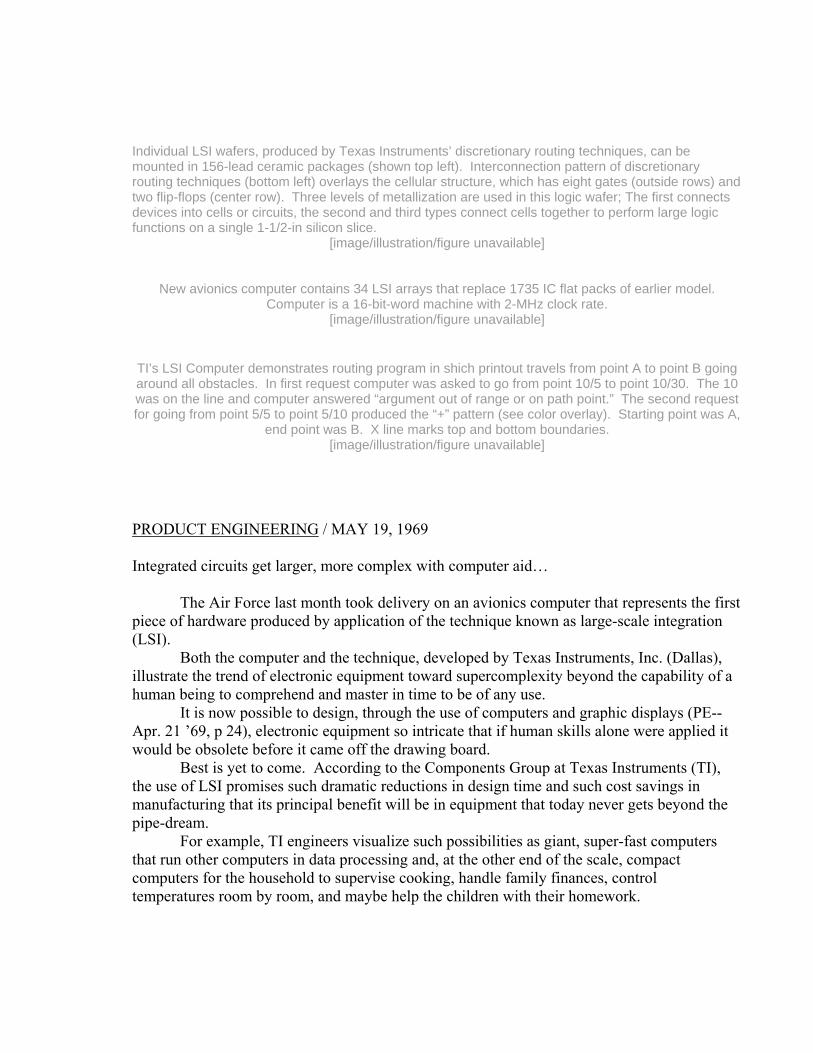
Individual LSI wafers, produced by Texas Instruments’ discretionary routing techniques, can be mounted in 156-lead ceramic packages (shown top left). Interconnection pattern of discretionary routing techniques (bottom left) overlays the cellular structure, which has eight gates (outside rows) and two flip-flops (center row). Three levels of metallization are used in this logic wafer; The first connects devices into cells or circuits, the second and third types connect cells together to perform large logic functions on a single 1-1/2-in silicon slice.
[image/illustration/figure unavailable]
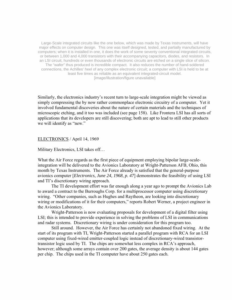
New avionics computer contains 34 LSI arrays that replace 1735 IC flat packs of earlier model. Computer is a 16-bit-word machine with 2-MHz clock rate.
[image/illustration/figure unavailable] TI’s LSI Computer demonstrates routing program in shich printout travels from point A to point B going around all obstacles. In first request computer was asked to go from point 10/5 to point 10/30. The 10 was on the line and computer answered “argument out of range or on path point.” The second request for going from point 5/5 to point 5/10 produced the “+” pattern (see color overlay). Starting point was A,
end point was B. X line marks top and bottom boundaries. [image/illustration/figure unavailable]
PRODUCT ENGINEERING / MAY 19, 1969 Integrated circuits get larger, more complex with computer aid… The Air Force last month took delivery on an avionics computer that represents the first piece of hardware produced by application of the technique known as large-scale integration (LSI). Both the computer and the technique, developed by Texas Instruments, Inc. (Dallas), illustrate the trend of electronic equipment toward supercomplexity beyond the capability of a human being to comprehend and master in time to be of any use. It is now possible to design, through the use of computers and graphic displays (PE-- Apr. 21 ’69, p 24), electronic equipment so intricate that if human skills alone were applied it would be obsolete before it came off the drawing board. Best is yet to come. According to the Components Group at Texas Instruments (TI), the use of LSI promises such dramatic reductions in design time and such cost savings in manufacturing that its principal benefit will be in equipment that today never gets beyond the pipe-dream. For example, TI engineers visualize such possibilities as giant, super-fast computers that run other computers in data processing and, at the other end of the scale, compact computers for the household to supervise cooking, handle family finances, control temperatures room by room, and maybe help the children with their homework.

Composite pattern of multi-layer discretionary routing on LSI wafer is generated by photomasking on cathode-ray tube hooked up to computer. System will quickly custom-design 1 or 1000 arrays of high-complexity logic as circuitry requires.
[image/illustration/figure unavailable] Packing a punch. LSI is a method of interconnection large numbers of discrete circuits or devices on a wafer of a material such as silicon, to handle a specific function, without separating the components. The interconnections are so complex that only a computer can design and test them. But this procedure eliminates the greatest expense in manufacture of solid-state equipment: the acres of drafting rooms and design laboratories and some production area. The computer works from the basic mathematical equations, the same ones that would otherwise require manual translation into circuit diagrams and then into prototypes. New computer. The new discretionary-routed LSI computer, chosen as a demonstration model for the Air Force, is similar to one previously built with conventional integrated circuits. It contains 34 arrays of 14 different types, averaging more than 200 transistor-transistor logic (TTL) gates per array. The 34 arrays supplant 1735 IC flat-packs. With 16 bits per word and a 2-MHz clock rate, the computer has been designed to be compatible with the Molecular Electronics for Radar Applications (MERA) radar system that’s being developed by the Air Force. The Air Force is concerned over the trend toward such complexity in equipment that failure of components and their interconnections imperils accomplishment even of some routine operations. The military people are equally concerned over the rapid increase in money, manpower, and time required for such support functions as supply, maintenance, and operator training. Hence the Air Force’s interest in development of ICs and especially of large-scale integration. Less to go wrong. Its thinking is that, with fewer interconnections, a system such as MERA will be subject to far fewer malfunctions, raising the reliability of the whole operation. The best way to reduce connections, the Air Force decided, was to take the molecular electronics approach, in which a piece of solid material is synthesized so as to perform a complete circuit function, as in the example of the IC. According to Robert M. Werner, project director of the Avionics Laboratory at Wright-Patterson Air Force Base, discretionary-routed LSI can now provide a practical means of breadboarding and perfecting design of digital equipment at much less cost than for the custom approach to development Aside from computers, the early applications of LSI may be in such real-time processing areas as communications receivers and airborne radar, Werner suggests. He foresees commercial applications in business and scientific computers, devices such as adding machines that use digital techniques, and perhaps switching circuits for tomorrow’s telephone systems. Advanced manufacture. Processing of an LSI wafer is similar to that of a wafer full of ICs, up to the point where testing of individual circuits is completed.

At this point, conventionally the wafer is cut apart, the chips are separately mounted and packaged, and the assortment is shipped to companies that then wire them into electronic systems. In the LSI process, the circuits are completed and tested under direction of computer, right on the intact wafer. The computer is programmed with the mathematical equations for the desired circuitry and also with instructions for placing the appropriate ICs on the wafer. It calculates the connections required to join the available chips into the desired circuit. It also generates the routing pattern for two or more layers of conductors in a metallization step to link the many elements on the wafer into a finished LSI circuit. Graphic display. These conductor patterns, the discretionary routing in an LSI, are generated by the computer on the face of a cathode-ray tube, from which a photographic mask can be made of each level of conductors. From the masks, these routes are reproduced in metal too fine to be assembled by any other method. Working out the routing alone would take months of high-paid human labor. When computers do most of the job, production-ready circuitry in discretionary-routed displays can be turned out in weeks.
Individual LSI wafers can be mounted in a 156-lead ceramic package like this. Unit cells can be fabricated separately or in combination on the 1-1/2 in. dia. wafer.
[image/illustration/figure unavailable]
With discretionary-routed LSI, one monolithic silicon array with packaging density of over 100 gates per
square inch can replace printed circuit board containing more than 80 IC flat packs. [image/illustration/figure unavailable]
FORTUNE – May 15, 1969 SOME OF THE YEAR’S NEW PRODUCTS While the 500 largest industrials obviously have plenty of competition in new-product development, their laboratories still come up with an extraordinary proportion of the new goods and systems that hit the market every year. All the new products in this portfolio were developed by the 500; all were marketed or tested during the past year. There is no very satisfactory way to differentiate between a totally new product and a mere refinement or modification of an existing one. Versatile synthetic fibers, for instance, are as old as nylon – i.e., they have been around for thirty years – but Tenneco’s Frontera is made from sculptured polymers, by an entirely different process, can do a number of things that no fiber has ever done before, and altogether seemed quite a lot “newer” than other recent fibers. (It is displayed in the pictures at the right.)
Large-Scale integrated circuits like the one below, which was made by Texas Instruments, will have major effects on computer design. This one was itself designed, tested, and partially manufactured by
computers; when it is installed in one, it does the work of some seventy conventional integrated circuits, or between 1,000 and 4,000 transistors with their accompanying capacitors, diodes, and resistors. In an LSI circuit, hundreds or even thousands of electronic circuits are etched on a single slice of silicon.
The “wafer” thus produced is incredible compact. It also reduces the number of hand-soldered connections, the Achilles’ heel of any complex electronic circuit; a computer with LSI is held to be at
least five times as reliable as an equivalent integrated-circuit model. [image/illustration/figure unavailable]
Similarly, the electronics industry’s recent turn to large-scale integration might be viewed as simply compressing the by now rather commonplace electronic circuitry of a computer. Yet it involved fundamental discoveries about the nature of certain materials and the techniques of microscopic etching, and it too was included (see page 158). Like Frontera LSI has all sorts of applications that its developers are still discovering; both are apt to lead to still other products we will identify as “new.” ELECTRONICS / April 14, 1969 Military Electronics, LSI takes off… What the Air Force regards as the first piece of equipment employing bipolar large-scale-integration will be delivered to the Avionics Laboratory at Wright-Patterson AFB, Ohio, this month by Texas Instruments. The Air Force already is satisfied that the general-purpose avionics computer [Electronics, June 24, 1968, p. 47] demonstrates the feasibility of using LSI and TI’s discretionary wiring approach. The TI development effort was far enough along a year ago to prompt the Avionics Lab to award a contract to the Burroughs Corp. for a multiprocessor computer using discretionary wiring. “Other companies, such as Hughes and Raytheon, are looking into discretionary wiring or modifications of it for their computers,” reports Robert Werner, a project engineer in the Avionics Laboratory. Wright-Patterson is now evaluating proposals for development of a digital filter using LSI; this is intended to provide experience in solving the problems of LSI in communications and radar systems. Discretionary wiring is under consideration for this program too. Still around. However, the Air Force has certainly not abandoned fixed wiring. At the start of its program with TI, Wright-Patterson started a parallel program with RCA for an LSI computer using fixed-wired emitter-coupled logic instead of discretionary-wired transistor-transistor logic used by TI. The chips are somewhat less complex in RCA’s approach, however; although some arrays contain over 200 gates, the average density is about 144 gates per chip. The chips used in the TI computer have about 250 gates each.
Handy, New TI airborne computer is about half size of old version [image/illustration/figure unavailable]
RCA’s program will be completed next month, on schedule, according to Werner. With TI, the Air Force also asked for a three-year program, but TI engineers felt they could do it in two. As it turned out, they had to ask for a year’s extension. “It did take longer than we anticipated,” says TI’s Jack Kilby, “because of the difficulty of getting all the technologies to work together.” Kilby is referring to the combined problems of partitioning, computer routing of interconnections, mask making, multilevel metallization, and packaging.
All lined up. A composite of the two masks for a typical circuit in the Computer. CRT traces the hundreds of paths in just 132 seconds. [image/illustration/figure unavailable]
TI plans to exploit commercially the techniques it developed during the program. The company will introduce in the next few months such discretionary-wired LSI circuits as a digital differential analyzer, a 1,000-bit shift register, and an eight-bit adder. As far as the TI’s LSI computer effort, the Air Force wasn’t too concerned about the piece of equipment used to prove LSI feasibility, according to Werner. “We just wanted one that would present the realistic problems in the development of the circuit and the partitioning of the arrays – getting the right logic on the chip.” The computer was “just a convenient vehicle” to demonstrate discretionary-wired LSI, he noted. Solution. TI, the prime advocate of the discretionary wiring technique, views it as a solution to the yield problem in LSI. Instead of using a fixed metallization pattern to interconnect the 100-or-more circuits on the chip, TI uses a computer to do the metallization layout. The computer remembers where the defective circuits are and avoids them when it designs the interconnection pattern. Although critics regard discretionary wiring as overly complex, expensive, and – at best – an interim solution, TI now points to actual hardware as a vindication of its technique. The computer uses 34 LSI arrays of 14 different types. The arithmetic section uses 16 of one type,……..[NOTE: Continued on next page – which is missing.] ELECTRONIC DESIGN – April 12, 1969 Air Force computer uses LSI arrays…
An avionics computer, with 34 large-scale-integration arrays replacing integrated-circuit flat-packs in a previous design, is being delivered to the Air Force this month. The 16-bit-per-word machine with a 2-MHz clock rate was built by Texas Instruments under a $2.1-million contract. The Air Force will use the computer as part of its MERA (Molecular Electronics for Radar Applications) solid-state radar systems, now under development. Fourteen types of discretionary-routed LSI bipolar arrays are used in the computer, with an average of over 200 TTL logic gates per array. The project – designated that complex arrays can be fabricated on 1-1/2-inch silicon wafers; that an automatic probe system can determine the exact location of every gate and flip-flop, and that an automatic test program can verify proper functioning of the completed array. Three levels of metallization are used in the array design. The first layer connects devices into circuits or cells; the other two interconnect cells to achieve the desired function. RESEARCH/DEVELOPMENT – May 1969 Discretionary Routing Makes Small-Run LSI Practical… Delivery of an avionics computer to the Air Force by Texas Instruments last month can be viewed as a large step towards increased reliability and perhaps lower cost of complex electronic circuits. Replacing 1735 integrated circuit flat packs of an earlier model of the computer were 34 LSI’s (large-scale integrated circuits) with an average of over 200 logic gates each. This represents reductions of 10:1 in interconnections and 70:1 in packaging operations. More important, 14 types of circuits were represented by the 34 arrays; these were produced by a technique called discretionary routing from only two basic LSI wafers. One type contains 128 flip-flops and 646 NAND gates on a 1-1/2-inch diameter wafer; the other, over 1000 master-slave flip-flops for use as a shift register. After circuits have been formed on the wafer, it is tested and the test results fed into a computer. Then the computer is instructed as to the type of function to be performed, it then controls equipment that generates a unique set of masks for interconnecting the circuits on a particular wafer so that that function will be performed. William E. Wickes of Texas Instruments sees the result of this approach as “a very definite low volume type of product as contrasted with the high volume requirements generally associated with IC components,” and talks of producing 1 or 1000 arrays “at a cost well below that normally required for custom implementation.” Could this make LSI circuits feasible for scientific instrumentation? BUSINESS WEEK – April 5, 1969
Cramming circuits onto a tiny silicon chip… (T)he art of large-scale integration (LSI) – has been given a new twist that could speed the miniaturization of electronic products. Texas Instruments, Inc., recently demonstrated a computer consisting of 34 LSI chips, each containing a variety of circuits. It was developed under an Air Force contract to prove TI’s “discretionary routed array” process. This is a computer-aided method of designing the conducting metal pattern that puts the largest possible number of circuits on each chip. It also means that logic chips can be furnished to order on six to eight weeks’ notice. By 1970, says TI, lead time could be down to a week. DATA SYSTEMS NEWS – April 1969 The 1969 IEEE International Convention and Exhibit held in New York, Mar. 24-27, was said to attract 65,000 engineers from around the world. Over 200 papers were read in 52 technical sessions. Among the introductions were a new avionics computer using large-scale integration (LSI) by Texas Instruments, Inc.; an electrically operated car from Alden (Electronics) Self-Transit; from 3M Co. a dry record system for oscillography; so-called hardened integrated circuits by radiation introduced by Radiation Inc.; and the use of a laser beam by RCA to transfer TV pictures and scientific electronic data to photographic film 40 times sharper than on home sets. TECHNICAL SURVEY WEEKLY, April 5, 1969 Texas Instruments new aircraft computer built with LSI electronic circuits, containing 34 LSI circuits, vs 1735 integrated circuits previously. A circuit on a wafer the dia(meter) of a 50 (cent) coin can do the work of 1000-4000 transistors, 1500 diodes and over 5000 resistors (12a). …..New airliner wing designed to reduce drag: the Brit “aft-loading concept” is being used on BAC’s Three-Eleven short-haul jetliner to improve lift and reduce drag. This wing is simpler in design and less ambitious in performance than NASA’s new “supercritical” wing (Financial Times (London), 2/12, p 24. CONTROL ENGINEERING – MAY 1969 AF Gets LSI Computer From Texas Instruments… New York – Still another significant step has been taken toward the “computer on a chip.” At a joint press conference, Texas Instruments, and U.S. Air Force officials unveiled an operating computer built with 34 lsi (large scale integration) wafers. Development of the new

computer, known as the TI 2502, is due in large part to the final success of “discretionary wiring” techniques pioneered by TI several years ago. This scheme permits the interconnection of good circuits on a typical 1.5-in. diam silicon wafer via these steps: O A wafer with a number of logic cells (say flipflops and gates) is made. O All cells on the wafer are tested and the location of good cells is noted and stored on tape in a computer. O The customer’s logic diagram is examined and a computer generates an optimum interconnection pattern based on the location of good cells. O Using this pattern, the computer, by means of a crt, prepares the interconnection masks (one horizontal and the other vertical). O Finally, wiring of the good cells is done. O The wafer is then tested in accordance with the customer’s logic diagram. Demonstrating the feasibility of this technique is a 16-bit computer with 2-Mcps clock rate. It will become a part of the MERA (Molecular Electronics for Radar Applications) radar system now being developed by the Air Force. To the commercial market, TI is offering its expertise in a similar way. Say a computer manufacturer presents TI with a set of logic diagrams. TI then will select suitable lsi wafers from their “shelf” and make the desired logic configurations. Maximum integrity for customer and vendor is assured: TI does not even have to know what the logic is intended for. The company simply produces the required number of units (and in fairly short time – six weeks’ delivery is presently envisioned) and then and there ends its involvement with the customer. At the present time there are two standard lsi slice types available: logic and the shift register. The logic slice contains 128 J-K flipflops and 648 one-, three-, five-, and seven-input NAND gates. The shift register slice can be used to obtain 253-bit registers or two 501-bit shift registers. Tab 3 – Digital Differential Analyzer – August 1969 TI NEWS RELEASE NR 324 FOR IMMEDIATE RELEASE AUGUST 21, 1969 TEXAS INSTRUMENTS INCORPORATED 13500 NORTH CENTRAL EXPRESSWAY DALLAS, TEXAS COMPONENTS GROUP CONTACT: Jon Campbell
In Dallas (214) 238-3741 Bill Groves In Houston (713) 522-9871 LSI DIGITAL DIFFERENTIAL ANALYZER – Special Purpose Computer HOUSTON, August 21…A Digital Differential Analyzer (DDA) computing unit on a single slice of silicon using discretionary Large Scale integration routing technology is available from Texas Instruments. The DDA is a special-purpose, incremental computer for the solution of differential equations. Inter-connection of two of these DDA’s will provide the incremental solution to the sine and cosine functions. This is accomplished by having one DDA compute the sine while the other unit computes the cosine. It is particularly suited to any application where radian measurements are required such as a radar antenna or a machine tool control. To produce a large improvement in speed and interfacing capability, the type DRA 1001 (DDA) incorporates a 10 bit up-down binary counter and 10 bit add-subtract accumulator (essentially, the accumulation is a 10 bit adder-subtractor with a 10 bit output buffer). It also incorporates a directional control with two independent inputs, a sign bit output (which also feeds into the direction controls internally), and a special false count suppression circuit which prevents ambiguous conditions from occurring. The DDA 1001, even at 253 equivalent gates, represents only a medium complexity LSI array (note that a flip-flop is considered as six equivalent gates). When two DRA 1001 DDA units are cross-connected properly, they will accept a serial incremental radian measurement, such as the pulse train from an Azimuth Change Pulse (ACP) generator connected to a radar antenna, and compute the relevant sine-cosine pairs at roughly one milliradian increments. Since digital computations are unaffected by temperature, voltage variations, etc., the output depends only on the incremental radian steps. The DDA’s have been designed with high speed TTL parallel logic implementation and can operate with an input clock rate of 2 MHz. The resolution on the input angular pulse is better than 1 milliradian. Power dissipation is approximately 2.1 watts per array and it operates from a 5 V dc power supply. Evaluation quantities of the DDA are available 8 weeks after receipt of order at a price of $750.00 each in 1 to 4 quantities. The DDA is supplied in a 156-pin ceramic package.
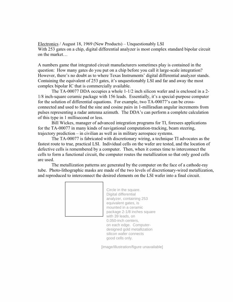
Electronics / August 18, 1969 (New Products) – Unquestionably LSI With 253 gates on a chip, digital differential analyzer is most complex standard bipolar circuit on the market… A numbers game that integrated circuit manufacturers sometimes play is contained in the question: How many gates do you put on a chip before you call it large-scale integration? However, there’s no doubt as to where Texas Instruments’ digital differential analyzer stands. Containing the equivalent of 253 gates, it’s unquestionably LSI and far and away the most complex bipolar IC that is commercially available. The TA-00077 DDA occupies a whole 1-1/2 inch silicon wafer and is enclosed in a 2-1/8 inch-square ceramic package with 156 leads. Essentially, it’s a special-purpose computer for the solution of differential equations. For example, two TA-00077’s can be cross-connected and used to find the sine and cosine pairs in 1-milliradian angular increments from pulses representing a radar antenna azimuth. The DDA’s can perform a complete calculation of this type in 1 millisecond or less. Bill Wickes, manager of advanced integration programs for TI, foresees applications for the TA-00077 in many kinds of navigational computation-tracking, beam steering, trajectory prediction – in civilian as well as in military aerospace systems. The TA-00077 is fabricated with discretionary wiring, a technique TI advocates as the fastest route to true, practical LSI. Individual cells on the wafer are tested, and the location of defective cells is remembered by a computer. Then, when it comes time to interconnect the cells to form a functional circuit, the computer routes the metallization so that only good cells are used. The metallization patterns are generated by the computer on the face of a cathode-ray tube. Photo-lithographic masks are made of the two levels of discretionary-wired metallization, and reproduced to interconnect the desired elements on the LSI wafer into a final circuit. Circle in the square. Digital differential analyzer, containing 253 equivalent gates, is mounted in a ceramic package 2-1/8 inches square with 39 leads, on 0.050-inch centers, on each edge. Computer- designed gold metallization silicon wafer connects good cells only.
[image/illustration/figure unavailable]

The DDA slice contains 128 J-K flip-flops and 646 one-, three-, five-, and seven-input NAND gates. TI describes the unmetalized IC as a “general-purpose logic slice” that can be used to implement any logic function of up to 250-gate complexity. Besides the DDA, it can be used for a 20-bit up-down synchronous counter and an eight-bit adder with look-ahead entry, for example. The DDA is an outgrowth of a program that TI conducted for the Air Force to develop an LSI computer [Electronics, April 14, p. 56]. It’s only the first in a series of LSI circuits that TI will introduce commercially [Electronics, Aug. 4, p. 33]. Although the company’s marketing men believe that almost all LSI circuits will be custom designed, they’re introducing standard LSI products anyway. The reason: experience has taught them that before users will order custom designs, they want the reassurance provided by standard, commercially available circuits.
Sine and cosine. Two DDA’s can be hooked up to compute the sine and cosine functions pertaining to radar antenna position. Navigation is the prime
field of applications for the DDA-on-a-chip. [image/illustration/figure unavailable]
With a 90-day delivery time, TI isn’t claiming “off-the-shelf” availability. This lead time, however, is shorter than for custom-designed circuits. Price is $750 for quantities of one to four. Because the manufacturer is marketing the circuits as design samples, it does not expect many orders in excess of this quantity. The TA-00077 includes as built-in features a 10-bit up-down binary counter and a 10-bit add-subtract accumulator. It has direction control inputs, a sign-bit input (which also feeds the direction control internally), and a false-count suppression circuit that prevents cumulative error resulting from rounding-out. The DDA utilizes high-speed parallel-transistor logic, and operates at a clock rate of 2 megahertz. Recommended supply voltage Vcc is 4.5 to 5.5 volts; at 5 volts, power dissipation is 2.5 watts. Operating case-temperature range is -55º to +125ºC. The low output voltage, at -8 milliamperes and a 5.5-volt Vcc, is no more than 0.4 volts. High output voltage, at 4 ma and 4.5-volt Vcc is at least 2.4 volts. With a “load” defined as 1.6 ma, the circuit can fan out to at least 5 loads. The antenna count pulse (ACP) fan-in, the external directional control (D′) fan-in, and the internal directional control fan-ins (X and Y) are two loads each. Fan-ins are 1 load each for Count, Nmax, and Nzero (which set the up-down counter to all 1’s and all 0’s, respectively), “true north” synchronizing pulse T′N, and accumulator synchronizing pulses NPA and NPB. ELECTRONIC NEWS – 8/25/69 – COMPUTER SECTION
TI Develops Chip Analyzer Houston. — A digital differential analyzer (DDA) computing unit on a single slice of silicon, has been developed by Texas Instruments. The DDA, using discretionary large-scale integration routing technology; is a special-purpose incremental computer {undecipherable}… of differential equations. Inter-connection of two of these DDAs will provide the incremental solution to the sine and cosine functions. This is accomplished by having one DDA compute the sine while the other unit computes the cosine. The unit is particularly suited to any application where radian measurements are required, such as a radar antenna or a machine tool control, TI said. The DDA, designed with high-speed TTL parallel logic implementation, can operate with an input clock rate of 2 MHz. The resolution on the input angular pulse is better than 1 mrad. Power dissipation is about 2.1 W per array and operates from a 5-V dc power supply. Evaluation quantities of the DDA, available l8 weeks after receipt of order, are priced at $750 each in quantities of 1 to 4. The DDA is supplied in a 156-pin ceramic package. ELECTRONICS WORLD / Dec., 1969 LARGE-SCALE INTEGRATION by David L. Heiserman — Is this the beginning of the LSI era? Here are some of the problems confronting semiconductor manufacturers in going to LSI, along with the main features of presently available LSI devices.
LSI Instruments In April 1969, Texas Instruments delivered the first LSI computer system to the U.S. Air Force. The system contains 34 LSI packages that replace 1735 IC’s needed for an earlier version of the same system. The LSI packages are divided into 14 different kinds of circuits, fabricated from only two different wafers. One of the wafers contains 128 flip-flops and 646 nand gates on a 1-1/2” monolithic chip while the other chip contains over 1000 flip-flop shift-register elements. The 14 different packages were made from two basic monolithic LSI chips by a programmable discretionary routing technique. This LSI computer system represents a 10:1 reduction in the number of circuit interconnections and a 70:1 decrease in the number of circuit assembly operations. If LSI circuits do indeed represent the last logical step in the evolution of semiconductor technology, it follows that future laboratory efforts will be devoted mainly to producing larger, more complex, and less costly LSI devices and systems.
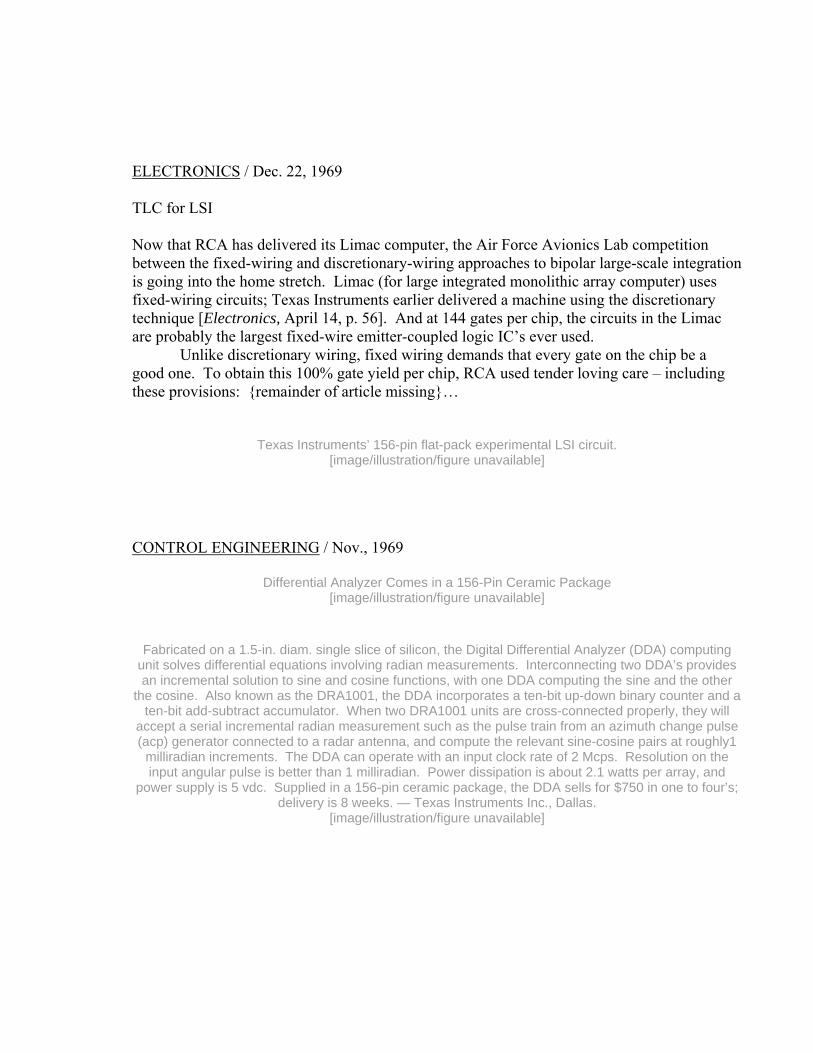
ELECTRONICS / Dec. 22, 1969 TLC for LSI Now that RCA has delivered its Limac computer, the Air Force Avionics Lab competition between the fixed-wiring and discretionary-wiring approaches to bipolar large-scale integration is going into the home stretch. Limac (for large integrated monolithic array computer) uses fixed-wiring circuits; Texas Instruments earlier delivered a machine using the discretionary technique [Electronics, April 14, p. 56]. And at 144 gates per chip, the circuits in the Limac are probably the largest fixed-wire emitter-coupled logic IC’s ever used. Unlike discretionary wiring, fixed wiring demands that every gate on the chip be a good one. To obtain this 100% gate yield per chip, RCA used tender loving care – including these provisions: {remainder of article missing}…
Texas Instruments’ 156-pin flat-pack experimental LSI circuit. [image/illustration/figure unavailable]
CONTROL ENGINEERING / Nov., 1969
Differential Analyzer Comes in a 156-Pin Ceramic Package [image/illustration/figure unavailable]
Fabricated on a 1.5-in. diam. single slice of silicon, the Digital Differential Analyzer (DDA) computing unit solves differential equations involving radian measurements. Interconnecting two DDA’s provides an incremental solution to sine and cosine functions, with one DDA computing the sine and the other
the cosine. Also known as the DRA1001, the DDA incorporates a ten-bit up-down binary counter and a ten-bit add-subtract accumulator. When two DRA1001 units are cross-connected properly, they will
accept a serial incremental radian measurement such as the pulse train from an azimuth change pulse (acp) generator connected to a radar antenna, and compute the relevant sine-cosine pairs at roughly1
milliradian increments. The DDA can operate with an input clock rate of 2 Mcps. Resolution on the input angular pulse is better than 1 milliradian. Power dissipation is about 2.1 watts per array, and
power supply is 5 vdc. Supplied in a 156-pin ceramic package, the DDA sells for $750 in one to four’s; delivery is 8 weeks. — Texas Instruments Inc., Dallas.
[image/illustration/figure unavailable]

PROGRESS IN MICROELECTRONICS New discretionary-wired DDA IC comes in 156-pin square flat-pack In another impressive demonstration of what can be done with discretionary wiring, Texas Instruments has announced the availability of a 156-pin monolithic DDA. The new bipolar DDA (digital differential analyzer), designated the DR1001, is called the equivalent of 253 gates (equivalency is based on comparable complexity: a flip-flop, for example, is considered the equivalent of six gates). The DR1001 is intended for applications involving radian measurements such as would be required for radar antenna and some industrial and machine-tool controls. The DDA is an incremental computer designed to solve differential equations. By interconnecting two of the TI DDA ICs, the engineer can obtain the incremental solution for sine and cosine functions (one DDA computes the sine, the other the cosine).
TI DR1001 IC, a digital differential analyzer, is the equivalent of 253 gates. [image/illustration/figure unavailable]
Two properly connected DR1001 ICs can accept a serial incremental radian measurement, such as the pulse train from an azimuth-change-pulse (ACP) generator connected to a radar antenna, and compute the applicable sine-cosine pairs at approximately 1-milliradian increments. Since digital computations are unaffected by temperature or voltage variations in a properly designed system, the output will depend only on the incremental radian steps. Counter plus accumulator The DRA1001 contains a 10-bit up-down binary counter and a 10-bit add-subtract accumulator (essentially, the accumulator is a 10-bit adder-subtractor with a 10-bit output buffer). The IC also includes a directional control with two independent inputs, a sign bit output (which also feeds into the direction controls internally), and a false-count suppression circuit which prevents ambiguous conditions from occurring. Rated for an input clock rate of 2 MHz, the DRA1001 can be implemented by TTL parallel logic such as provided by Series 54/74 ICs. The resolution on the input angular pulse is better than one milliradian. The IC is operated from a 5-Vdc power supply; it dissipates approximately 2.1 W. In quantities of 1-4 units, the DRA1001 sells for $750. Eight weeks should be allowed for delivery.
Discretionary-wired LSI The DR1001 joins a select group of discretionary-wired IC’s built by TI and packaged in 156-pin ceramic flat packs. Other devices, also supplied in the 156-pin case, include a quad 253-bit array and a dual 349-bit array. The quad 253-bit array, available for about a year, contains approximately 4300 transistors and 4300 resistors, 1800 inter-level connections, 70 inches of second-level metallization and 20,000 cross-overs. To figure out the interconnection schemes for its discretionary-wired ICs, TI uses a computer-driven CRT mask-making system called MIG (Multi-level Interconnection Generating System). The MIG is fed probe data revealing the locations of good circuits along with the desired array configuration. Using this information, it produces a routing-program output tape which determines the mask layout.
[image/illustration/figure unavailable]
ELECTRONIC PRODUCTS / NOV 1, 1969 Digital differential analyzer… Type DRA-1001 digital differential analyzer is contained on a single silicon slice and makes use of discretionary wiring. It is for use as a special-purpose incremental computer for the solution of differential equations. Package is a 156-pin ceramic atpack. Unit incorporates a 10-bit up-down binary counter and 10-bit add-subtract accumulator. Also a part of the circuit is a directional control with two independent inputs, a sign bit output and a special false count suppression circuit. Basic logic is TTL, allowing an input clock rate of 2 Mhz. Power dissipation is 2.1 w. Price: $750 ea (1 to 4). Avail: 8 wk. Mfr: Texas Instruments, Incorporated. Other Products: See eem pp 2602-2619. MACHINE DESIGN / SEPT. 1969 – Page 106
A true computer on a chip, this LSI digital differential analyzer, manufactured by Texas Instruments, Dallas, Tex, solves differential equations. Two of them can be connetedto solve sine and cosine
functions. These special-purpose computers, intended for use in such applications as radar systems and machine tools are forerunners of tomorrow’s miniaturized general-purpose machines.
[image/illustration/figure unavailable] EDN – Oct. 1, 1969

Digital Differential Analyzer DRA 1001 is fabricated on a single slice of silicon that uses discretionary
LSI routing technology. [image/illustration/figure unavailable]
The unit is a special-purpose incremental computer for the solution of differential equations and includes a 10-bit up-down binary counter, 10-bit add-subtract accumulator, directional control with two independent inputs, a sign-bit output and a special false-count suppression circuit that prevents ambiguous conditions from occurring. The unit operates with an input clock rate of 2 MHz. Power dissipation is approximately 2.1 W/array and operation is from a 5V dc power supply. In quantities of 1 to 4 units, price is $750 each for the 156-pin ceramic-package unit. electronic products / November 1, 1969 Digital differential analyzer Type DRA-1001 digital differential analyzer is contained on a single silicon slice and makes use of discretionary wiring. It is for use as a special-purpose incremental computer for the solution of differential equations. Package is a 156-pin ceramic flatpack. Unit incorporates a 10-bit up-down binary counter and 10-bit add-subtract accumulator. Also a part of the circuit is a directional control with two independent inputs, a sign bit output and a special false count suppression circuit. Basic logic is TTL, allowing an input clock rate of 2 Mhz. Power dissipation is 2.1 w. Price: $750 ea (1 to 4). Avail: 8 wk. Mfr: Texas Instruments, Incorporated. Other Products: See eem pp 2602-2619. MARKET COMMUNICATIONS / Oct. 1969 – p. 75 Coming from TI: discretionary-wired shift registers…and 16 more TTL devices Texas Instruments isn’t wasting time. Just last summer it introduced the first commercial discretionary-wired product, an LSI digital differential analyzer [Electronics, Aug. 18, p. 145]. Making their bow next month will be three dynamic bipolar devices – a dual 253-bit unit, a dual-349 device, and a dual-501 unit. They will sell initially for about 40 cents per bit in medium quantities, but TI officials see the price dropping to less than 20 cents per bit in the next two years. Unlike the DDA introduced first, which has three layers of metallization, these products have only two metal layers, one of which is discretionary routed.

TI is also continuing to fill out its nondiscretionary wired transistor-transistor logic line. Sixteen more products will be unveiled by year’s end, four of which employ two layers of metallization. These devices – a synchronous decade counter, a synchronous binary counter, a six-bit binary rate multiplier, and a 64-bit read-write memory – have been furnished on a custom basis. Jack Carsten, TTL marketing manager, says Fairchild has also sold some custom devices using two layers of metal, but the new TI products will be available in production quantities. And, he says, the two-layer devices will be medium- and large-scale integrated TTL. Carsten expects the extra cost of a second metal layer to be offset by higher yield because the dies can be made smaller. TI won’t use two layers of metal for “much less than 50 gates,” Carsten says. Aviation Week & Space Technology / September 1, 1969 Complete digital differential analyzer built on a single silicon chip, containing 253 bi-polar gates, is being introduced by Texas Instruments. Two such devices can be used to compute sine and cosine functions from digital pickoff in a radar antenna, for example. The device operates at an input clock rate of 2 mc, and has a resolution of better than one milliradian. The Type DRA-1001 comes in a ceramic flat-pack with 156 leads. Tab 4 – High Speed Shift Registers (November, 1969) TI NEWS RELEASE NR 330 FOR IMMEDIATE RELEASE TEXAS INSTRUMENTS INCORPORATED 13500 NORTH CENTRAL EXPRESSWAY DALLAS, TEXAS COMPONENTS GROUP CONTACT: Jon Campbell In Dallas
(214) 238-3741 Bill Groves In Houston (713) 522-9871 HIGH SPEED LSI SHIFT REGISTERS Houston, November 3, 1969….Three long bit lengths are now available from Texas Instruments in the new Large Scale Integrated shift registers. These are the first bipolar LSI shift registers ever offered for sale. Standard units include a dual 253, a dual 349, and a dual 501-bit shift registers using standard TTL circuitry with TI’s exclusive discretionary routing technology to interconnect individual shift register cells on a single monolithic 1 ½-inch diameter slice of silicon. Custom lengths are also available. The Discretionary Route Arrays (DRA) have very short internal connections which minimizes capacitive coupling resulting in high noise immunity. These LSI shift registers operate from dc to 10 MHz over the full temperature range of -55 to +125ºC. Special internal low voltage circuitry has greatly reduced power dissipation per bit resulting in a very high speed-to-power ratio. The repetitive nature of the shift register circuits make it feasible to produce very long registers with all of the inherent high reliability, speed, and design flexibility of conventional Series 54 TTL circuitry. The shift registers contain cells of four bits each discretionarily routed in series plus an additional one-bit output driver. This makes chains available in lengths of (4N + 1) bits. LSI shift registers also offer a low cost per bit when compared to discrete and MSI assembled systems capable of comparable performance. Less than 40 cents per bit is easily realized with bipolar LSI shift registers. These registers are five times longer and 10 times faster than currently available static MOS shift registers.
LSI/DRA BIPOLAR SHIFT REGISTERS TYPE NUMBER OF BITS PRICE 100 TO 249 QTY DRA-2001 Dual 253 $295.00 Each DRA-2002 Dual 349 $335.00 Each DRA-2003 Dual 501 $390.00 Each Arrays are packaged in standard 78-pin 2 1/8-inch square ceramic package. Small quantity delivery is quoted as eight weeks ARO. NOTE TO THE EDITOR: To help us respond quickly to your readers requests

For additional information, please send inquiries to: Texas Instruments Incorporated Inquiry Answering Service P. O. Box 5012 – M/S 308 Dallas, Texas 75222 To avoid unnecessary delays in forwarding inquiries, PLEASE DO NOT SENT TO ANY OTHER ADDRESS.
[image/illustration/figure unavailable]
COMPUTER DESIGN / NOVEMBER 1969 (CD PRODUCT FEATURE) Bipolar LSI Shift Registers Offer Design Flexibility
TEXAS INSTRUMENTS, INC. [image/illustration/figure unavailable] Components Group Houston, Texas Three bipolar LSI shift registers from Texas Instruments now make it feasible to produce very long shift registers with all the inherent reliability, speed and flexibility of conventional Series 54 TTL circuitry. Standard units include a dual 253, a dual 349 and a dual 501-bit register using standard TTL logic with TI’s discretionary routing technology to interconnect individual register cells on a monolithic slice of silicon 1 ½ inches in diameter. Discretionary routing minimizes capacitive coupling resulting in high noise immunity. The LSI registers operate from dc to 10 MHz over the full temperature range of -55 to +125ºC, and a special internal low voltage circuitry greatly reduces power dissipation per bit resulting in a very high speed-to-power ratio. Cells of four bits each discretely routed in series plus an additional one-bit output driver compose each register. This makes chains available in lengths of (4N + 1) bits. Representative of the registers is the DRA-2002, a dual 349-bit serial-in serial-out device. The two shift register chains are independently clocked by two sets of clock drivers included in the array. Also contained in the array is an output buffer stage at the end of each chain which insures output levels compatible with the Series 54 TTL and provides fan-out of 5 from both true and complement outputs. Internally, the master-slave shift register bits are operated by a two phase clock system (ø-master clock, ø-slave clock). Clock drive for each phase is developed by drivers on the
array. ø1 and ø2 are not allowed in the 0 state simultaneously, for, if they are, data will ripple through more than one stage. Both true and complement data must be supplied. Data is clocked into the first bit upon the transition of ø1 from logical 1 to logical 0. Transfer of information to the output terminals occurs when ø1 goes from a logical 0 to a logical 1.
Functional diagram of DRA-2002, dual 349 shift register for 78-pin package. [image/illustration/figure unavailable]
Recommended Operating Conditions Min Typ Max Units Supply voltage Vcc (Note 1) 4.5 5.0 5.5 V Supply voltage Vbb (Note 1) 2.2 2.4 2.6 V Fan-out from each output 5 Width of any clock pulse 40 ns Clock frequency 0 10 MHz Price and Delivery Type NUMBER OF BITS PRICE 100 to 249 QTY DRA-2001 Dual 253 $295.00 Each DRA-2002 Dual 349 $335.00 Each DRA-2003 Dual 501 $395.00 Each Arrays are packaged in a standard 78-pin 2 ½-inch square ceramic package. Small quantity delivery is quoted as eight weeks ARO. Electronics / December 8, 1969 COMPONENTS GROUP MARKET COMMUNICATIONS
NEWS CLIPS Concerning TI Products, Processes or people
At last, a bipolar shift register with the same bit capacity as MOS
At 1,000 bits per wafer, discretionary-wired bipolar IC’s not only match
MOS circuits in complexity but also surpass them in shift rate with no need for data refreshing; speeds of 40 MHz are possible. By Roger Dunn & Glenn Hartsell Texas Instruments, Dallas Why would anyone want a bipolar shift register integrated circuit with 1,000-bit capacity when excellent MOS IC’s are already available at a lower price? There are compelling reasons; only bipolar circuitry combines the virtues of speed with the capacity for long periods of storage. It’s true that metal oxide semiconductor shift registers are attractive when dynamic storage can be used, but in many systems this isn’t possible; data must wait for long periods between shifting. And if the system operates at high speed, static MOS is no alternative, since it has only a fraction of the speed of a dynamic MOS shift register unless the complicated technique of multiplexing is used. Furthermore, static MOS occupies more chip area per function, and consumes more power than dynamic MOS. The design of the clock distribution line also becomes critical. In short, MOS of this type offers few of the advantages usually attributed to MOS technology as a whole. Then there’s the added complication of extra power supplies and buffer circuitry to interface MOS with transistor-transistor logic. Bipolar circuitry, then, is the answer in high-speed, high capacity, static shift registers. And this is the approach that Texas Instruments selected for an airborne digital-signal-processing application, in which shift registers are needed for video integration to replace analog delay lines, for digital filtering in moving-target indication to eliminate range-gate analog analog filters, and for correlation. A thousand bits on a bipolar chip is certainly large-scale integration, and is probably the most ambitious of current advanced integration projects. A typical 1,000-bit shift register contains 9,000 components, 1,800 feedthroughs, 20,000 crossovers, and 70 inches of metal just in one of the two inter-connection layers. This complexity is only possible at this stage of bipolar technology through the use of discretionary wiring, a highly automated technique in which only good cells are interconnected on the chip. [Electronics, Feb. 20, 1967, page 143]. Discretionary wiring increases the component density of bipolar circuits by two orders of magnitude and also greatly reduces the power consumption per bit because internal circuitry can be operated at lower voltage levels. At 16 megahertz, the new shift register operates at 3 milliwatts per bit, or one-eight of the power level of the SN5491 eight-bit TTL shift register. The speed of the LSI 1,000-bit register is much greater than that of a register of the same capacity made from several conventional integrated circuits. This is because the propagation delay caused by connections between IC’s is eliminated. Thus, the LSI register can operate at the 16 MHz shift rates. Moreover, multiplexing with TTL circuits can be done very simply because of the similar input and output levels, and with this technique, shift rates in excess of 40 MHz can be attained.

Predictably, the extremely large number of components on the chip – and their density – created some critical questions that had to be resolved by the design engineers: ▪ What circuit should be selected for the basic shift register cell that would be tolerant of wide variations in device parameters and thus give a high yield of good cells? ▪ Could a power supply distribution network be designed that could handle the 2 amperes that flow into the circuit without excess voltage drop? ▪ What would be the optimum number of cells per stage that will neither waste chip real estate nor adversely affect yield? The circuit selected for the basic bit is composed of simple master and slave flip-flops with four resistors and four multiple-emitter transistors per bit, shown on page 87. This cell operates from a two-phase clock and the voltage difference between the two input signals. The clock signals are timed so that they’re never high simultaneously. When clock 1 is high, the low side of the input from previous bits (or from the input to the chain) sets the master flip-flop. When the clocks are reversed, clock 1 is low and the master data is stored, producing a differential output signal VBE-VCE(sat) -- the difference between base-emitter voltage and the collector-emitter saturation voltage. Now, with clock 2 high, this differential signal sets the slave, and current from both master and slave flows into the clock 1 line. To make sure that the differential signal from each flip-flop is enough to trigger the following one, the transistors’ base resistance is made rather high so that VBE-VCE(sat) equals VBE, the local forward-biased base-collector voltage. This high base resistance has the added advantage of limiting the saturation current and the leakage of the reverse-biased emitters. Occupation. LSI bipolar shift register occupies entire 1-1/2 inch slice of silicon. For efficient distribution
of signals and power, clock drivers are arrayed in center of wafer, output buffers at edge. Circuit contains 9,000 components.
[image/illustration/figure unavailable] One of the transistors in a bistable will be in saturation, and hence produce an output difference, as long as: hFE > 2VBB - 2VCL - 2VCE(sat)
2VBB - 2VCL - 2VBE - 2VCE(sat) This equation pertains to bistables with matched resistors, as is the case in IC’s. VBB is the power supply voltage, and VCL is the clock voltage. This equation explains why the cell has such a high immunity to parameter variation. It can still operate without loss of information with, for example, current gain, hFE, less than 10 and VBB as low as 1.7 volts. The relationship between speed and power is always a vital concern in digital circuits, and the basic cell selected for the shift register offers excellent performance in this respect. At a shift rate of 16 MHz, the array dissipates only 3 mw per bit.
Slowest set the pace Actually, in a large-capacity shift register, the maximum shift rate is determined by the slowest bit in the chain, not by the typical bit. The parameter-variation tolerance of the basic bit, shown on page 87, stands it in good stead here too; it will operate at high speed (10 MHz or more) over a VBB power supply range of 2.0 to 2.8 volts. The discretionary wiring technique helps maintain a high shift speed, since it detects slow bits during probe testing and prevents them from being connected in the chain. Power supply distribution was an extremely important issue as the large number of bits requires the distribution of a large total current – large for an IC. Use of differential signals at the input and outputs of the bistables helps somewhat. Nevertheless, the circuit must handle 1 amphere total current for each of the two clock drivers. The solution was to scatter 20 clock drivers with 60 milliampere ratings across the wafer, paralleling the inputs and outputs. This number of clocks in parallel would be impossible with discrete IC’s, because the parameter variations from circuit to circuit would introduce skew problems in which the time separation between clock edges at two adjacent flip-flops is excessive. But in an LSI circuit, with clock cells on the same slice, the variations are small. To further aid in distribution, the wafer is laid out with the clocks in the center, dividing the wafer in two equal halves. Locating the clocks in the center minimizes the voltage drop along the clock lines and reduces lead congestion at the periphery of the wafer. An output buffer is required to translate the low-level output from the shift register to TTL levels. Again, to minimize voltage drop and also to conserve wafer area, these output buffers are located at the edge of the wafer. Unfortunately, this is where wafer defects are most numerous, and yields are therefore lower than on the rest of the wafer. To compensate, extra output circuits are put on the wafer. The distribution bus leads for ground, power supplies, and clock are contained in the first of the two metallization layers (the first metal layer also contains the intra-cell connections). For any functional combination of cells, the maximum voltage drop is 125 mv on ground lines, 100 mv on power lines, and 50 mv on clock lines.
(block diagram) Application. One use of TI’s 1,000-bit circuit is as a delay unit in a two-stage filter with feedback for an
airborne moving-target indicator. [image/illustration/figure unavailable]
The basic bit occupies an area 0.014 by 0.014 inch. It would be inefficient to probe-test each bit individually, since test pads would have to be provided for each and would take up too much area (test pads are 0.003 inch square, and seven would be needed for each bit.) Instead, groups of bits should be connected in stages, with one set of input and output pads for each stage. Setting the stage
The question is how many bits should be connected in a stage. On the basis of the data plotted on facing page, Texas Instruments selected a stage length of four bits. A shorter stage – two bits, for example – would occupy too much area per bit, as indicated by the number of good circuits per square inch on the vertical axis of the diagram. This effect becomes more pronounced at higher yields.
{stage length matrix} Effect of stage length on yield and inter-layer connections
[image/illustration/figure unavailable] On the other hand, longer stages such as eight bits provide efficient utilization of surface area as long as the yield is very high, but this utilization efficiency drops off drastically if the yield is lower. The four-bit stage is the best compromise. With test-pads, it requires only 9% more area per bit than an eight-bit stage, and the number of good stages per square inch varies much less with yield than for the eight-bit stage. The output buffers and the clocks function individually, not in stages. There are 48 clock drivers for each half of the wafer. This is enough to drive 1,200 bits in each half, or 2,400 bits for the entire wafer. Even if the yield of clock cells were as low as 70%, there would still be enough to drive 850 bits in each half. The situation isn’t really this simple, however, because an uneven distribution of good circuits has to be taken into account. For example, if two clock frequencies are used for all bits in a quad 253 array, as in the TI 1,000-bit register, each quadrant must have 12 good clock drivers. So it’s not enough for the wafer to have at least 48 good clock drivers; they must have to be distributed appropriately, too. In general, clock-cell yield and the geometrical distribution of the yield are no problem, largely because the center of the wafer, with its relatively low defect density, is a favorable location.
(shift register schematic) Bit. Basic unit of shift register is a master-slave flip-flop (light color). Four such bits are combined to
form a stage. [image/illustration/figure unavailable]
Extra buffers provide margin There are 48 output buffers. Each quadrant has two segments as shown on page 85, one with eight buffers and the other with four. To keep yield from becoming a problem in the unfavorable portions of the wafer in which the buffers are located, many extra buffer cells are provided. Only one good buffer is needed in each segment, corresponding to a 25% yield in the four-buffer segments and 12.5% in the longer ones.
(graph)
Optimum. Selection of stage length is a compromise between conserving wafer area and obtaining an adequate number of good stages.
Texas instruments uses four bits per stage in its shift register. [image/illustration/figure unavailable]
Closely related to the question of optimum bit length for the shift register stages was the problem of making connections between the metalization layers. Selection of a four-bit stage length for the shift register means that eight inter-layer connections are needed per 0.0023 square inch, or 2,975 feedthroughs per square inch. This density is well within the capability of the cathode-ray tube technique for generating metalization masks and of the metal deposition process. Metalization line width is 0.002 inch, and the minimum separation between lines is 0.002 inch. A two-bit stage length, however, would place excessive demands on the multilayer-metalization process, requiring a feedthrough density of 5,230 per square inch.
{Insert Multilevel image here.} Multilevels. Good bits are interconnected by means of two metal layers separated by an oxide layer. For conductivity and adhesion, the metal layers are composites of gold, molybdenum, and aluminum.
[image/illustration/figure unavailable] The lower metallization level is an aluminum-molybdenum-gold-molybdenum composite, selected to give both adhesion and high conductivity. The upper metallization layer is similar but lacks the top skin of molybdenum, since it’s not needed for adhesion. Separating the two metallization layers is a 15,000-angstrom-thick layer of silicon dioxide with 0.0006-inch diameter feedthrough holes.■ Complex IC development has been the major work of Roger Dunn and Glenn Hartsell, who wrote the
article starting on page 84. Dunn is manager of custom MSI programs at Texas Instruments; his particular interest is computer-aided (design) of TTL memories, both main frame and scratch pad, for TI.
Hartsell has been in LSI since joining TI in 1966; he helped develop a prototype of the shift register described in the article. He now heads the LSI design section.
[image/illustration/figure unavailable] ELECTRONICS / DEC 8, 1969 Technical Articles – Solid state At last, a bipolar shift register with the same bit capacity as MOS At 1,000 bits per wafer, discretionary wired bipolar IC’s not only match MOS circuits in complexity but also surpass them in shift rate with no need for data refreshing; speeds of 40 MHz are possible.

Roger Dunn and Glenn Hartsell, Texas Instruments ELECTRONIC NEWS / Monday, Nov. 10, 1969 New Bipolar Shift Registers by TI Houston. -- Texas Instruments has introduced a series of bipolar shift registers, here. The dual 253-, 359- and 501-bit registers use standard TTL circuitry and TI’s discretionary routing technology. Discretionary routed arrays interconnect individual shift register cells on a single 1½-inch diameter slice of silicon, TI said. The registers operate from dc-10 MHz over -55º to +125º C. Price range is $295-$390 for 100-249, depending on type and number of bits. AMERICAN MACHINIST / Dec. 1969 Small, expensive package… Riddle: What is 1½ in. in diameter, under 1/10 in. thick, operates at any temperature from 55º below zero to 125º C above, and costs $390.00? Only in quantities of 100 to 250, at that “volume” price. The answer is a bipolar LSI shift register, which is a kind of integrated electronic circuit made by Texas Instruments. Exactly what it does and what its circuit diagram looks like no rational mechanic would want to know. But it is an advance in the state of the computer art, and it will ultimately have a reducing effect on costs. And, our NC experts say, it is really a giant abacus for lightning-speed counting. CIRCUITS MANUFACTURING / Oct., 1969 EXOTICA – LSI DIGITAL DIFFERENTIAL ANALYZER Scouting around for a special purpose incremental computer on a single slice of silicon that provides the solution to differential equations? You’re in luck. Inter-connection of two of these Digital Differential Analyzers (DDA’s) provides the incremental solution to the sine and cosine functions. The DRA 1001 (DDA) incorporates a 10 bit up-down binary counter and 10 bit add-subtract accumulator and incorporates a directional control with two independent
inputs, a sign bit output (which also feeds into the direction controls internally) and a special false count suppression circuit which prevents ambiguous conditions from occurring. DDA’s use high speed TTL parallel logic implementation, operate with an input clock rate of 2 MHz and offer resolution on the input angular pulse better than 1 milliradian.
[image/illustration/figure unavailable] Power dissipation, approx 2.1 w/array. Unit operates from a 5 v dc power supply and comes in a 156-
pin ceramic package.
Price: $750 each in quantities of 1 to 4. Delivery, 8 wks. Texas Instruments, Inc., P.O. Box 5012, Dallas, Tex. 75222. (214) 238-3741. ELECTRONIC DESIGN / Dec. 1969 (New SC’s)
LSI shift registers operate to 10 MHz [image/illustration/figure unavailable]
Texas Instruments, Inc. Box 5012-MS308, Dallas, Tex. P&A: $295, $335 or $$390 per 100; 8 wks. Three new bipolar LSI shift registers, including a dual 253-bit, a dual 349-bit and a dual 501-bit model operate from dc to 10 MHz over a temperature range of -55 to +125º C. Types DSA-2001, -2002 and -2003 are packaged in a 78-pin, 2-1/8 in. – square ceramic package and contain cells of four bits each discretionally routed in series plus a one-bit output driver. ELECTRONIC DESIGN / Dec. 1969
[image/illustration/figure unavailable] New SC’s High speed LSI Shift Registers include a dual 253-, a dual 349- and a dual 501-bit register. By using standard TTL circuitry and discretionary routing technology, shift-register cells are interconnected on a single monolithic 1-1/2-in-diam slice of silicon. Units operate from dc to 10 MHz over the range -55 to 125º C and are packaged in a standard 78-pin, 2-1/8-in-square ceramic package. Prices are $295 (dual 253), $335 (dual 349) and $390 (dual 501), in lots of 100 to 249. Texas Instruments Incorporated*

*Texas Instruments Incorporated, Inquiry Answering Service, Box 5012, M.S. 308, Dallas, Tex. 75222 WEN / Dec. 1969, p. 36 High speed LSI shift registers ■ Three long bit lengths have been made available by Texas Instruments in new bipolar Large Scale Integrated shift registers. The company said they are the first bipolar shift registers ever offered for sale. Standard units include a dual 253, a dual 349, and a dual 501-bit shift registers using standard TTL circuitry with TI’s exclusive discretionary routing technology to interconnect individual shift register cells on a single monolithic 1½ in. diameter slice of silicon. Custom lengths also are available. The firm said the discretionary routed arrays have very short internal connections which minimize capacitive coupling resulting in high noise immunity. The registers operate from dc to 10 MHz over the full temperature range of -55 to +125ºC.
[image/illustration/figure unavailable] Special internal low voltage circuitry, the company stated, has reduced power dissipation per bit resulting in a very high speed-to-power ratio. The repetitive nature of the shift register circuits makes it feasible to produce very long registers with all of the inherent high reliability, speed and design flexibility of conventional Series 54 TTL circuitry. (Texas Instruments, Inc., Inquiry Answering Service, O.O. Box 5012, M/S 308, Dallas, Texas 75333) Tab 5 – Major Articles ELECTRO-TECHNOLOGY / OCT 1969 Emerging technology – large scale integration in systems design – bipolar technology (by William E. Wicks, Manager, Advanced Integration Programs, Texas Instruments Inc., Dallas) A new technology – the ability to create complete logic networks on a single monolithic silicon structure – is born. The complete large scale integration (LSI), discretionary-routed arrays duplicate the effect of interconnecting logic circuits in packages on a multilayer printed circuit board. The importance of this rapidly growing technology is covered in this article.

The rate-of-change in electronic equipment, since the development of the transistor, has no technological parallel. The transistor, still a young device, has been outpaced by integrated circuit. The large-scale integration, discretionary-routed array (LSI/DRA) is a natural extension of integrated-circuit technology. The evolution of electronics Although innovations in electronic equipment have been most prolific since the transistor, review of all stages in the evolution is necessary to properly understand the significance of LSI, the fourth generation of electronic components. The vacuum tube, the first generation electronics, is a result of man’s curiosity into the control of electric fields and emerged in the early 20th century. The components associated with tube circuits have gone through numerous materials changes in efforts to improve stability and performance, but the resistor remains a component which reacts in accordance to Ohm’s law. Transistors, the second generation electronics, were developed in 1948 at Bell Laboratories by the American physicists William Shockley, Walter Brattain, and John Bardeen. They are the result of investigations into semiconducting materials. Subsequent research has produced solid-state devices which can be used to perform almost all the functions of the vacuum tube at greatly reduced power requirements and with much higher reliability.
Author Bill Wickes exhibits the standard LSI packaging with epoxy-sealed lid. [image/illustration/figure unavailable]
The integrated circuit, electronics’ third generation, was invented by Jack Kilby of Texas Instruments in 1958. It was made possible by the fact that resistors and capacitors can be formed from the same semiconductor material which is used to produce the transistor. The transistor, resistors, and capacitors make up the active and passive elements of a circuit. By processing all three components in a silicon substrate and subsequently joining them with low-resistance metallization, a complete circuit is realized. ICs yield high circuit densities The silicon substrate (semiconductor material) usually is in the form of a thin slice of silicon cut from a round rod of pure crystal silicon. The area required by the integrated circuit is minuscule relative to the silicon slice, so many integrated circuits are fabricated on a single slice of silicon at the same time.
ICs BEGIN with a grown silicon rod
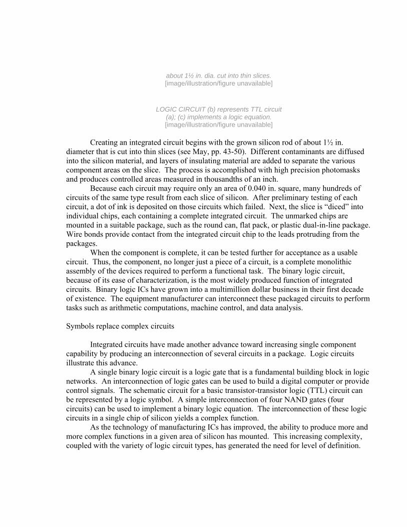
about 1½ in. dia. cut into thin slices. [image/illustration/figure unavailable]
LOGIC CIRCUIT (b) represents TTL circuit (a); (c) implements a logic equation. [image/illustration/figure unavailable]
Creating an integrated circuit begins with the grown silicon rod of about 1½ in. diameter that is cut into thin slices (see May, pp. 43-50). Different contaminants are diffused into the silicon material, and layers of insulating material are added to separate the various component areas on the slice. The process is accomplished with high precision photomasks and produces controlled areas measured in thousandths of an inch. Because each circuit may require only an area of 0.040 in. square, many hundreds of circuits of the same type result from each slice of silicon. After preliminary testing of each circuit, a dot of ink is deposited on those circuits which failed. Next, the slice is “diced” into individual chips, each containing a complete integrated circuit. The unmarked chips are mounted in a suitable package, such as the round can, flat pack, or plastic dual-in-line package. Wire bonds provide contact from the integrated circuit chip to the leads protruding from the packages. When the component is complete, it can be tested further for acceptance as a usable circuit. Thus, the component, no longer just a piece of a circuit, is a complete monolithic assembly of the devices required to perform a functional task. The binary logic circuit, because of its ease of characterization, is the most widely produced function of integrated circuits. Binary logic ICs have grown into a multimillion dollar business in their first decade of existence. The equipment manufacturer can interconnect these packaged circuits to perform tasks such as arithmetic computations, machine control, and data analysis. Symbols replace complex circuits Integrated circuits have made another advance toward increasing single component capability by producing an interconnection of several circuits in a package. Logic circuits illustrate this advance. A single binary logic circuit is a logic gate that is a fundamental building block in logic networks. An interconnection of logic gates can be used to build a digital computer or provide control signals. The schematic circuit for a basic transistor-transistor logic (TTL) circuit can be represented by a logic symbol. A simple interconnection of four NAND gates (four circuits) can be used to implement a binary logic equation. The interconnection of these logic circuits in a single chip of silicon yields a complex function. As the technology of manufacturing ICs has improved, the ability to produce more and more complex functions in a given area of silicon has mounted. This increasing complexity, coupled with the variety of logic circuit types, has generated the need for level of definition.

For purposes of this article, the following terminology is adopted. The conventional integrated circuit (IC) is assumed to contain one to 12 equivalent logic gates. Medium scale integration (MSI) is a device containing from 12 to less than 100 equivalent gates. Large scale integration (LSI) is a package containing 100 or more equivalent gates. These definitions refer to a monolithic structure of semiconductor material and do not include hybrid assemblies. The packaged chip or bar of silicon which can be produced economically has now grown to about 0.125 in. on the side. The diameter of the silicon slice which is processed has increased from the original 1 in. diameter to 2 and sometimes 2½ in. There have been reports of silicon rods as large as 3 in. being grown for sawing into slices. This increase in both the diameter of the basic silicon slice and in the area of the single packaged chip is an attempt to take advantage of the batch processing of ICs and create more logic circuits at lower prices. The size of a single-circuit-function chip is limited by yield. A 2-in. slice can contain 2,000 chips which are 0.040 in. square or about 300 chips which are 0.100 in. square. Assuming a 5% yield, this results in 100 or 15 chips, respectively. If it cost $50 to process the slice and produce the chips, the 0.040 in. square chip will cost 50¢ while the 0.100 in. square chip will cost $3.33. This procedure can be extended to a chip which is 0.200 in. square. There can be about 80 chips of this size in a 2 in. wafer (ignoring edge loss) and this will yield (at 5%) 4 chips. At $50 for the process, the individual chips will cost $12.50. But these assumptions ignore the fact that defects in semi-conductor processing are random in number and size. This means that yield of a 0.200 in. square bar is significantly less than the yield of a 0.040 in. square bar. Because of the decreased yields, trying to produce large size circuits where the circuit must be 100% good before it can be useful becomes uneconomical. Discretionary routing to produce ICs The discretionary routing approach to large scale integration conceived by TI in 1964 is based upon the following concepts: □ A large number of small area circuits can be processed on a slice of silicon. □Circuits do not necessarily have to be of the same type; i.e., different circuit types can be fabricated on a slice of silicon at the same time by a common process. □ Circuits can be tested as part of the slice of silicon to a degree sufficient to identify the good circuits. □ A computer program can be developed which will generate automatically an inter-connection pattern of randomly located good circuits to form a large block of circuits. □ This computer program can accomplish the task in an economical and reliable fashion. □ Precision cathode ray tube photomask generation equipment can be invented which would make the required multilevel metallization and insulation masks at a low cost.
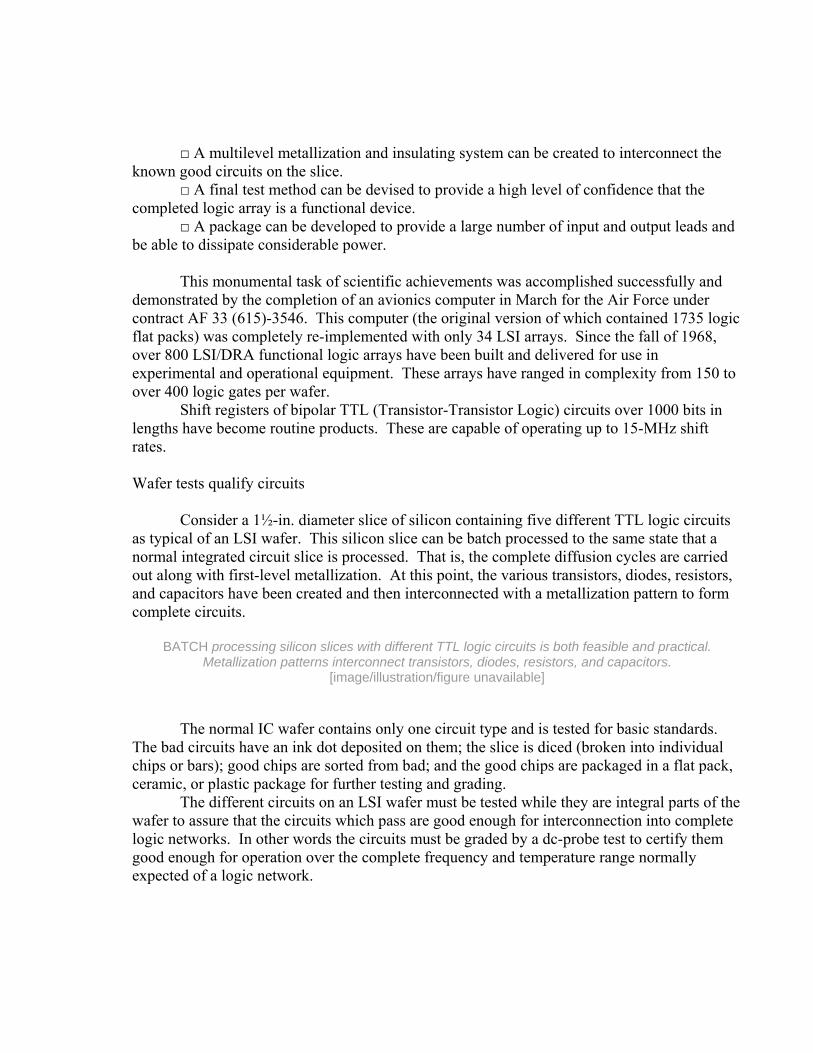
□ A multilevel metallization and insulating system can be created to interconnect the known good circuits on the slice. □ A final test method can be devised to provide a high level of confidence that the completed logic array is a functional device. □ A package can be developed to provide a large number of input and output leads and be able to dissipate considerable power. This monumental task of scientific achievements was accomplished successfully and demonstrated by the completion of an avionics computer in March for the Air Force under contract AF 33 (615)-3546. This computer (the original version of which contained 1735 logic flat packs) was completely re-implemented with only 34 LSI arrays. Since the fall of 1968, over 800 LSI/DRA functional logic arrays have been built and delivered for use in experimental and operational equipment. These arrays have ranged in complexity from 150 to over 400 logic gates per wafer. Shift registers of bipolar TTL (Transistor-Transistor Logic) circuits over 1000 bits in lengths have become routine products. These are capable of operating up to 15-MHz shift rates. Wafer tests qualify circuits Consider a 1½-in. diameter slice of silicon containing five different TTL logic circuits as typical of an LSI wafer. This silicon slice can be batch processed to the same state that a normal integrated circuit slice is processed. That is, the complete diffusion cycles are carried out along with first-level metallization. At this point, the various transistors, diodes, resistors, and capacitors have been created and then interconnected with a metallization pattern to form complete circuits.
BATCH processing silicon slices with different TTL logic circuits is both feasible and practical. Metallization patterns interconnect transistors, diodes, resistors, and capacitors.
[image/illustration/figure unavailable] The normal IC wafer contains only one circuit type and is tested for basic standards. The bad circuits have an ink dot deposited on them; the slice is diced (broken into individual chips or bars); good chips are sorted from bad; and the good chips are packaged in a flat pack, ceramic, or plastic package for further testing and grading. The different circuits on an LSI wafer must be tested while they are integral parts of the wafer to assure that the circuits which pass are good enough for interconnection into complete logic networks. In other words the circuits must be graded by a dc-probe test to certify them good enough for operation over the complete frequency and temperature range normally expected of a logic network.
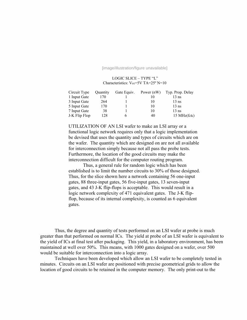
[image/illustration/figure unavailable]
LOGIC SLICE – TYPE “L” Characteristics: Vcc=5V TA=25º N=10
Circuit Type Quantity Gate Equiv. Power (nW) Typ. Prop. Delay 1 Input Gate 170 1 10 13 ns 3 Input Gate 264 1 10 13 ns 5 Input Gate 170 1 10 13 ns 7 Input Gate 38 1 10 13 ns J-K Flip Flop 128 6 40 15 MHz(fclk) UTILIZATION OF AN LSI wafer to make an LSI array or a functional logic network requires only that a logic implementation be devised that uses the quantity and types of circuits which are on the wafer. The quantity which are designed on are not all available for interconnection simply because not all pass the probe tests. Furthermore, the location of the good circuits may make the interconnection difficult for the computer routing program. Thus, a general rule for random logic which has been established is to limit the number circuits to 30% of those designed. Thus, for the slice shown here a network containing 56 one-input gates, 88 three-input gates, 56 five-input gates, 13 seven-input gates, and 43 J-K flip-flops is acceptable. This would result in a logic network complexity of 471 equivalent gates. The J-K flip-flop, because of its internal complexity, is counted as 6 equivalent gates.
Thus, the degree and quantity of tests performed on an LSI wafer at probe is much greater than that performed on normal ICs. The yield at probe of an LSI wafer is equivalent to the yield of ICs at final test after packaging. This yield, in a laboratory environment, has been maintained at well over 50%. This means, with 1000 gates designed on a wafer, over 500 would be suitable for interconnection into a logic array. Techniques have been developed which allow an LSI wafer to be completely tested in minutes. Circuits on an LSI wafer are positioned with precise geometrical grids to allow the location of good circuits to be retained in the computer memory. The only print-out to the
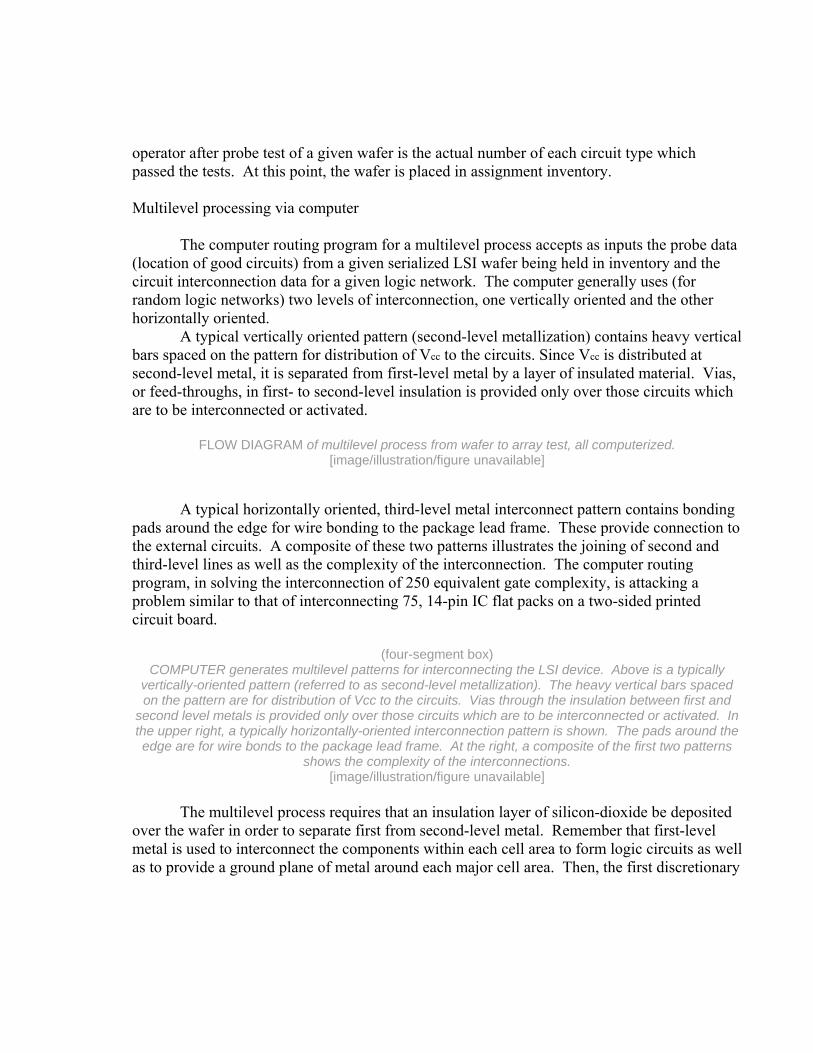
operator after probe test of a given wafer is the actual number of each circuit type which passed the tests. At this point, the wafer is placed in assignment inventory. Multilevel processing via computer The computer routing program for a multilevel process accepts as inputs the probe data (location of good circuits) from a given serialized LSI wafer being held in inventory and the circuit interconnection data for a given logic network. The computer generally uses (for random logic networks) two levels of interconnection, one vertically oriented and the other horizontally oriented. A typical vertically oriented pattern (second-level metallization) contains heavy vertical bars spaced on the pattern for distribution of Vcc to the circuits. Since Vcc is distributed at second-level metal, it is separated from first-level metal by a layer of insulated material. Vias, or feed-throughs, in first- to second-level insulation is provided only over those circuits which are to be interconnected or activated.
FLOW DIAGRAM of multilevel process from wafer to array test, all computerized. [image/illustration/figure unavailable]
A typical horizontally oriented, third-level metal interconnect pattern contains bonding pads around the edge for wire bonding to the package lead frame. These provide connection to the external circuits. A composite of these two patterns illustrates the joining of second and third-level lines as well as the complexity of the interconnection. The computer routing program, in solving the interconnection of 250 equivalent gate complexity, is attacking a problem similar to that of interconnecting 75, 14-pin IC flat packs on a two-sided printed circuit board.
(four-segment box) COMPUTER generates multilevel patterns for interconnecting the LSI device. Above is a typically
vertically-oriented pattern (referred to as second-level metallization). The heavy vertical bars spaced on the pattern are for distribution of Vcc to the circuits. Vias through the insulation between first and
second level metals is provided only over those circuits which are to be interconnected or activated. In the upper right, a typically horizontally-oriented interconnection pattern is shown. The pads around the edge are for wire bonds to the package lead frame. At the right, a composite of the first two patterns
shows the complexity of the interconnections. [image/illustration/figure unavailable]
The multilevel process requires that an insulation layer of silicon-dioxide be deposited over the wafer in order to separate first from second-level metal. Remember that first-level metal is used to interconnect the components within each cell area to form logic circuits as well as to provide a ground plane of metal around each major cell area. Then, the first discretionary

mask is one of vias through this insulation to provide connections between first and second-level metal. Often many thousands of vias are required. Both the first- and second-level metal interconnections are composed of a sandwich of molybdenum-gold-molybdenum about 17,000 ang thick and 2.5 mils wide. The molybdenum separates the gold conductor from the silicon insulation. This metallization was chosen, after much research, for its stability and current-carrying capacity. The third level discretionary interconnect, composed of molybdenum-gold, is also about 17,000 ang thick and 2.5 mils wide. The output from the computer discretionary-routing program is a set of instructions which will cause a direct-view cathode ray tube with a 1-mil spot to be deflected in x-y coordinated movements. A 2:1 reducing lens focuses this spot onto a 70-mm film strip. The camera shutter is left open during a given sequence so that all movements of the cathode ray tube spot are traced on the film. There are four basic sets of instructions from the computer program and subsequent film masks required for each wafer: a) set of vias in the insulation between first and second-level metal; b) second-level metal interconnections; c) set of vias in insulation between second- and third-level metal; and d) third-level metal. Then, the film is processed, cut into appropriate sections, and used as direct-contact masks on the serialized wafer for the multilevel metallization process. Array testing completes phase The final phase of the process of creating an LSI array is the testing of the completed array to verify that the interconnections are valid and that the array will perform in accordance with the logic diagram. TI has developed a “single-fault modeling” approach, since testing an input logic array with all possible combinations of inputs that can occur is impractical. However, testing for a single type of fault at each node within the logic network is both practical and effective. This approach assumes that a set of inputs can be defined which not only will exercise each circuit output but also will test for the output being stuck-at-one or stuck-at-zero. The number of tests required for a 200- to 400-gate array is in the thousands. But this is a reasonable number to generate and test through the use of computer programs and computer-controlled test equipment. The equipment at TI is capable of applying 5,000 tests per second to a 156 pin LSI. This approach to tests does not require knowledge of the functional capability of a logic array. Therefore, a logic diagram can be provided, the multilevel interconnection accomplished, and the completed array tested without the operator knowing what the array does functionally. This gives the customer confidence that his circuit innovations are protected. In addition, he is guaranteed that his information is treated on a proprietary basis. Packaging the LSI for industry
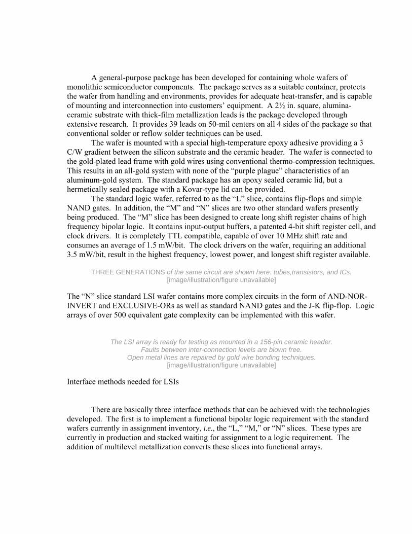
A general-purpose package has been developed for containing whole wafers of monolithic semiconductor components. The package serves as a suitable container, protects the wafer from handling and environments, provides for adequate heat-transfer, and is capable of mounting and interconnection into customers’ equipment. A 2½ in. square, alumina-ceramic substrate with thick-film metallization leads is the package developed through extensive research. It provides 39 leads on 50-mil centers on all 4 sides of the package so that conventional solder or reflow solder techniques can be used. The wafer is mounted with a special high-temperature epoxy adhesive providing a 3 C/W gradient between the silicon substrate and the ceramic header. The wafer is connected to the gold-plated lead frame with gold wires using conventional thermo-compression techniques. This results in an all-gold system with none of the “purple plague” characteristics of an aluminum-gold system. The standard package has an epoxy sealed ceramic lid, but a hermetically sealed package with a Kovar-type lid can be provided. The standard logic wafer, referred to as the “L” slice, contains flip-flops and simple NAND gates. In addition, the “M” and “N” slices are two other standard wafers presently being produced. The “M” slice has been designed to create long shift register chains of high frequency bipolar logic. It contains input-output buffers, a patented 4-bit shift register cell, and clock drivers. It is completely TTL compatible, capable of over 10 MHz shift rate and consumes an average of 1.5 mW/bit. The clock drivers on the wafer, requiring an additional 3.5 mW/bit, result in the highest frequency, lowest power, and longest shift register available.
THREE GENERATIONS of the same circuit are shown here: tubes,transistors, and ICs. [image/illustration/figure unavailable]
The “N” slice standard LSI wafer contains more complex circuits in the form of AND-NOR-INVERT and EXCLUSIVE-ORs as well as standard NAND gates and the J-K flip-flop. Logic arrays of over 500 equivalent gate complexity can be implemented with this wafer.
The LSI array is ready for testing as mounted in a 156-pin ceramic header. Faults between inter-connection levels are blown free.
Open metal lines are repaired by gold wire bonding techniques. [image/illustration/figure unavailable]
Interface methods needed for LSIs There are basically three interface methods that can be achieved with the technologies developed. The first is to implement a functional bipolar logic requirement with the standard wafers currently in assignment inventory, i.e., the “L,” “M,” or “N” slices. These types are currently in production and stacked waiting for assignment to a logic requirement. The addition of multilevel metallization converts these slices into functional arrays.
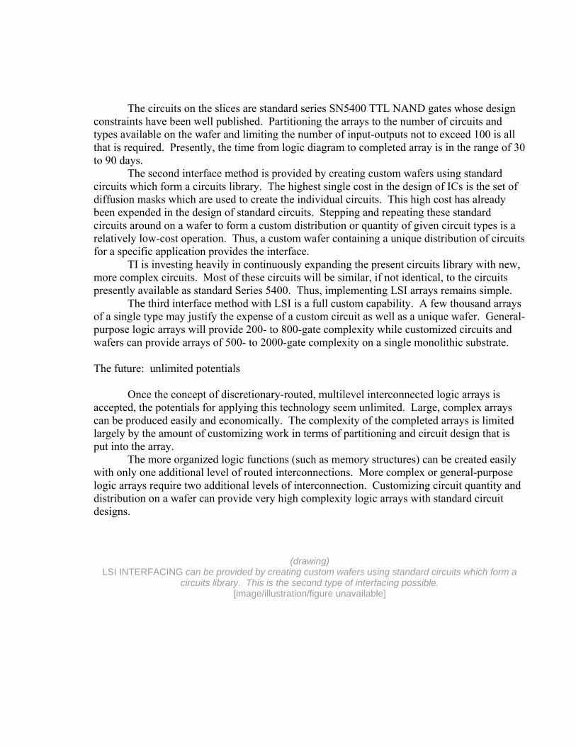
The circuits on the slices are standard series SN5400 TTL NAND gates whose design constraints have been well published. Partitioning the arrays to the number of circuits and types available on the wafer and limiting the number of input-outputs not to exceed 100 is all that is required. Presently, the time from logic diagram to completed array is in the range of 30 to 90 days. The second interface method is provided by creating custom wafers using standard circuits which form a circuits library. The highest single cost in the design of ICs is the set of diffusion masks which are used to create the individual circuits. This high cost has already been expended in the design of standard circuits. Stepping and repeating these standard circuits around on a wafer to form a custom distribution or quantity of given circuit types is a relatively low-cost operation. Thus, a custom wafer containing a unique distribution of circuits for a specific application provides the interface. TI is investing heavily in continuously expanding the present circuits library with new, more complex circuits. Most of these circuits will be similar, if not identical, to the circuits presently available as standard Series 5400. Thus, implementing LSI arrays remains simple. The third interface method with LSI is a full custom capability. A few thousand arrays of a single type may justify the expense of a custom circuit as well as a unique wafer. General-purpose logic arrays will provide 200- to 800-gate complexity while customized circuits and wafers can provide arrays of 500- to 2000-gate complexity on a single monolithic substrate. The future: unlimited potentials Once the concept of discretionary-routed, multilevel interconnected logic arrays is accepted, the potentials for applying this technology seem unlimited. Large, complex arrays can be produced easily and economically. The complexity of the completed arrays is limited largely by the amount of customizing work in terms of partitioning and circuit design that is put into the array. The more organized logic functions (such as memory structures) can be created easily with only one additional level of routed interconnections. More complex or general-purpose logic arrays require two additional levels of interconnection. Customizing circuit quantity and distribution on a wafer can provide very high complexity logic arrays with standard circuit designs.
(drawing) LSI INTERFACING can be provided by creating custom wafers using standard circuits which form a
circuits library. This is the second type of interfacing possible. [image/illustration/figure unavailable]

Radiation-hardened structures (which take relatively large silicon areas, multilevel metal resistors, and aluminum interconnections) appear to be suited naturally to the technologies which have been developed. Discretionary-routed, multilevel interconnections can provide semiconductor monolithic memories of huge sizes once a multi-level structure for MOS is developed. The short length of interconnections on the monolithic substrate is well suited to the high-speed requirements of ECL circuits. These radiation-hardened circuits, and many more, provide opportunities for application and exploration of discretionary-routed, multilevel technology.■ electronics products / december 1969
FORUM ON MSI/LSI by George Flynn, Senior Associate Editor Call it what you want – MSI, LSI or big IC – there’s a revolution in motion and it’s going to change everything by at least an order of magnitude. Maybe two.
FARR MINGIONE STEWART FARR of Data Systems – “I think most of the initial applications will be large quantities of LSI in small computers. Right now we see the greatest application of LSI/MOS in desk calculators. In a large computer you have the problem of partitioning so as to use a large number of devices repetitively, and this is going to be a complex applications problem.”
[image/illustration/figure unavailable] MINGIONE of American Micro-systems – “Sometimes a customer wants to duplicate exactly what he already has in his logic. But the best way is to work within the technology and use it to maximum advantage.” STEWART OF Hughes Aircraft – “Most of the applications in the military area tend to be small black boxes. If these are MOS you have to worry about driving a lot of capacitance, or you have high fan-out or similar things. There are so many interfacing circuits it hurts and you’re into problems in a hurry.” WHILE AGREEMENT about what MSI and LSI really are is hard come by, everybody agrees that they are the embodiment of the next revolution in electronics. They promise almost

everything you want in a circuit, but especially low cost and small size. Low cost means you can afford them; small size means you can have great complexity. LSI is new, really new, and very few of its characteristics – capabilities, limitations, cost effectiveness, reliability – are clearly understood. Some people believe LSI is going to shake down into a fairly well-defined group of standard building blocks, quite similar although more complex than IC’s. Others believe LSI devices will – almost by definition – always be custom. Many, many other questions can and will be raised about LSI before it finally is completely understood. One thing at least is certain: Electronics in the decade of the seventies is going to be slapped hither and thither by a very large tail called LSI. How complex can you get? One of the premises of LSI is that you can put more and more circuitry into fewer and fewer packages and thereby reap some important advantages; namely, lowest possible cost per circuit function, smallest possible size, and increased reliability. And strangely enough, all the advantages are real. You actually get them; and what you have to give up, at least to some extent, is well worth it. What, exactly, do you have to give up? What are the tradeoffs you make as you move toward ever more complex chips? And what, if any, are the limitations on complexity? Can we get all the complexity we can possibly use, or will we have to stop somewhere because technology fails us? Not all the answers are in, but some appear to be clear. Some idea of how complex LSI is today can be obtained from the table on page 29. Read-only memories with more than 2,000 bits, for example are available off-the-shelf. These are off-the-shelf devices, remember. Considerable greater complexity is available in custom devices. “With today’s technology,” says Richard Stewart of Hughes Aircraft, “that is, standard diffusion and masking tolerances, as opposed to the interconnecting approach (discretionary wiring), we can easily produce LSI devices having 500 or more bipolar gates. In the very near future – a couple of years at most – we will be able to have things like 8- to 16-thousand bits of random read-only memory (ROM) in MOS. And that does not assume that you are pushing basic technology in terms of basic diffusion techniques. But it does assume the addition of an interconnection approach such as discretionary wiring.” William Wickes, of Texas Instruments believes we are just at the beginning of the LSI game. “I think there is no question that the complexity will continue to accelerate as our technological and mask-making capabilities improve. MOS is probably going to have the most dramatic effect with respect to such things as devices per unit area. But I think we will also have some break-throughs in bipolar technology that will rival MOS. In our current discretionary wiring approach, for example, we have a dual shift register, where each bit is master-slave flip-flop. If you define each bit as four gates, you have 4,000 gates or 20,000 components. And those are only the ones we interconnect. So the limitation on LSI

complexity will not be technology, but the characteristics of the thing you’re making and the ability to interconnect them, whether they be hybrid, discrete components, beam leads, or what have you.” As parts get more and more complex, you eventually come up against the concept of a system on a chip – such as a TV set, a computer memory, or a spectrum analyzer. And you have to ask questions like: “How far do we really want to go?” Harry Schaffer of the Singer Co..’s Friden Div., has this viewpoint: “There’s no doubt that we can use a lot more complexity than we can get now. There are opportunities to reduce almost everything we build, if the technology were at the level where we could depend on getting IC’s (or MSI/LSI) that would do it. We could take a large size logic card and reduce it to one small IC package if technology would permit it. So I don’t see any limits on complexity coming up soon.” Richard Loumeau of TRW Systems says “we can use more complexity than can be provided, assuming you beg the question of maintainability and throw-away modules, which definitely are costs that have to be considered. If you want to put everything on one chip – and why not? – then the manufacturer will start to talk about yield and cost, and are you ever going to be able to get one unit off the end of the line? So while we’d like to put the whole system in one package, there are limitations that must be recognized and solved.”
{table) MOST COMPLEX OFF-THE-SHELF MSI/LSI DEVICE
[image/illustration/figure unavailable] Where we are The state of the art of MSI/LSI as revealed by a questionnaire mailed to all known manufacturers in the field is suggested by the table above. Note first of all that the chart is specifically limited to off-the-shelf devices. Within this limitation, the manufacturers came up with a total of 389 MSI’s and 58 LSI’s for a total of 447 MSI/LSI devices (exclusive of various packaging permutations). The availability of MSI/LSI devices is further illuminated by the second-source column where we find, so far as a company’s most complex device is concerned, that few second sources exist. However, the most complex circuits are also in general the newest, and thus the fact that a few second sources already exist for some devices may be considered encouraging rather than otherwise. (Note: Philco-Ford will second source Fairchild’s 930 MSI family, and will begin sampling after January 1, 1970. Electronic Arrays has a cross licensing agreement with North American Philips Corp.) Regardless of second sources, the total number of different types of MSI/LSI devices available today is small when compared with IC’s or transistors. Some companies, however, don’t even recognize off-the-shelf devices as LSI type circuits, so this adds another complication. The complexity of off-the-shelf devices ranges from several hundred equivalent components to 4,000, or from a few gates to several hundred; but valid comparisons along these lines appear difficult and perhaps impossible. Also, the number of pins per device varies widely, and while a large number of pins probably signifies complexity, a small number does not necessarily signify lack of same. Custom LSI devices having far greater complexity than anything shown in the table have already been built and many more are in the offing, but many of the people who are designing LSI into product today don’t want to talk much about it until they can announce a fait accompi.

Every manufacturer listed in the table, with the exception of National Semiconductor, makes custom LSI and even they make a few “specials” for unspecified customers. In addition, you can get custom LSI from Ragen Semiconductor (Check 707) and Collins Radio (Check 708). Playing somewhat the role of devil’s advocate in the complexity debate is Samuel Nissim, of Electronic Arrays. He’s for complexity all right, but he doesn’t want to get there in a troika pulled by maddened horses and driven by a sales-manager who has smoked too much LSI. Nissim speaks, for one thing, about the “cost of ownership” that a user must pay, and this includes such things as upkeep and maintenance – the classic worst-case being perhaps, the Minotaur, who devoured seven youths and seven maidens every year. “Even if you think can put the whole computer on a chip,” he says, “you’re making a mistake. I have been involved in that field a long time and I haven’t yet seen a computer where human error has not reflected itself in changes, and the changes are very costly. You have to anticipate changes and not ask for complexity that will make it costly to effect design changes. If you insist on complexity, with attendant inflexibility, it is going to cost you your shirt, maybe.” Nissim also sees another possible limitation on complexity. “Power dissipation in a given area may cause very serious problems, and I believe the complexity in the future is going to be limited more by the problems of thermal coupling between components on the chip than by the ability of technology to put more and more on a chip. Power limitation, however, is definitely not a problem today.” SULLIVAN of Raytheon Semiconductor “I think the main use for MSI/LSI will be standard circuits, not custom, and for the same reasons people use standard IC’s – cost and availability, and they can be tested. Obviously there will be some market for customs but the main thing will be standards. { photo } { photo } {photo}
Specializing in MOS technology, Electronic Arrays provides MSI and IC devices for digital circuits. Shown here is a typical 40-pin package.
[image/illustration/figure unavailable]
Custom vs Standard Probably no single decision agitates LSI users more than the choice between a custom and a standard device, and with it, the question of a second source. If you wait for a circuit to
become standard (meaning in wide use by many users) and thus with assured second sources, will your product, when you finally get in on the street be obsolete, or perhaps an also-ran? If you go the custom road, and your supplier for the LSI bugs out on you, whom do you run to? “But”, you may ask, “can’t I go custom, and then, if trouble comes, can’t I pick up my masks and go play on the other side of the street?” Maybe you can and maybe you can’t. It all depends on whom you want to believe. Let Robert Graham, of Intel, Inc., put the problem into perspective as he sees it. “Having a sole source is not the biggest problem. The biggest problem is, ‘Do you have a source at all?’ And if you do have a source, then you are not in too bad a shape. When we had transistor built by a jillion guys – all different technologies – it was very difficult to get two that looked alike. Today, that isn’t the case. Our interfaces are DTL or TTL and we know the levels they need; whether they are built one way or another doesn’t matter. If you pick a source, sole or otherwise, that can deliver, you will probably wind up with a second source just as quickly as the second guy can come along.”
[image/illustration/figure unavailable]
SIDORSKY – Left of General Instruments “For the large volume user customers are ideal because there is basically no waste. For the medium and small volume user standards are the way to go. I think the market is split half and half between custom and standard and I think its going to remain split.”
THACKER – Right of Berkeley Computer “One severe problem right now is the interface between the user and the manufacturer. The manufacturer says he can build us a 10,000-gate array, but we, as a user, have no feeling about how he can interconnect them. There is a very little information about this.”
{ photo }
In any case, the objective in the LSI game is to end up with a lot of circuit functions crammed into one small package. And how you get to that small package may not be too important. One way is to go hybrid, wherein a bunch of IC or MSI chips get hooked together before the whole kluge gets into a package. This kind of LSI is apparently just as good as any other kind. The classic concept of LSI, of course, is the 100% yield idea, where the circuit comes out of the furnace complete and ready for testing and packaging. The trouble here is that only about 1% to 5% of the chips cut from the wafer are 100% good – the other 95% to 99% of the chips are n.g. The discretionary wiring concept is an effort to reach LSI complexity by interconnecting IC size areas into LSI complexity chips. The IC areas are small enough to produce yields of 65% or so before dicing, thus the potential for improved yield per wafer is there. Before you can come out alive, however, you first have to test the wafer to locate the good IC’s, then you have to generate an interconnecting pattern to form the LSI, and then you have to generate the metallization masks to make the interconnections. And when the next wafer comes along, with a different pattern of good and bad IC areas, you’ve got to do the whole thing all over again.

Discretionary wiring sounds difficult, and tedious. And it probably would be if it weren’t for the computer, which does the whole thing including drawing the metallization patterns. But computers cost money and programming costs money, and so far the concept hasn’t been able to make it on the economics front. Not that it won’t. “We are selling thousands of discretionary-wired shift registers at $750,” says Wickes. “We also have a complete digital differential analyzer on a slice which we will sell at a sampling price of $750 – and well below that on quantity orders. Getting the price for the device down to about $100 will come very rapidly. It is really a question of how efficiently you can make the product. The costs are not in the front end of the product. They are in the interfacing and in the complexity of the testing process.” One of the paradoxes of LSI is that the more you put into one chip, the fewer chips you need, and thus you are reducing the possibility for large volume. The volume is not in the number of LSI chips, but in some abstraction compounded of number of chips times chip complexity. Gene Jones in the Microelectronic Products Div. of Autonetics, makes LSI chips. One of his potential customers is Don Farr, also of Autonetics, but in the Data Systems Div. “Don has capability within his own division,” says Jones, “to design custom circuits, but he can also get large volume custom circuits from our LSI manufacturing facility. Unfortunately, they don’t build a lot of airplanes these days, and certain circuits show up once per airplane. So we face some really severe problems caused by low volume. The most recent approach is to build some basic building blocks to which you then add a limited number of custom circuits to meet a unique, specific requirement.” Donald Farr then provided more details on how the building block concept has worked in practice. “Using these standard building blocks (each having about 200 terms, where each term is defined by a logic equation with one to 15 inputs) we’ve looked at a variety of machines using 16-, 24- or 32-bit words – both simple and complex construction sets – and we’ve been quite successful in mechanizing these machines out of the standard blocks, customizing only in the construction of micro-program controls. We think we will be successful with this approach and that the blocks will become good products for other people to use. HOMANN of Educational Computer
Corp. “Labor uncertainties and other hidden costs tend to make built-up circuits deceptively cheap on paper as they are expensive in equipment. An LSI array from multiple sources makes lots of sense and potentially lots of dollar too.” (photo)
(Undecipherable text) {photo)

[image/illustration/figure unavailable] IC, MSI or LSI? As circuit complexity per chip increases beyond what used to be usual for an IC, we run into the problem of what to call the new devices. As long as a seller and buyer of a complex chip know the specific circuit they’re working with, it doesn’t matter whether they call it IC, MSI or LSI – they’re still talking about the same thing. But when manufacturer A is selling you a glamorour LSI that is less complex than manufacturer B’s dowdy MSI or even prosaic IC, you the user may find yourself in a confusing and perhaps dangerous communications muddle – lost on a semantic sea. The solution to the semantic problem is simply a meeting of the minds among the various parties to any discussion about a complex chip. Here’s a sampling of what you can run into if you haven’t come to an agreement on what you’re talking about: Wickes: “We have tried to establish that LSI is greater than 100 gates, MSI is 12 to 100 gates and IC’s are one to 12. We are not necessarily making any distinction between hybrids, monolithic, MOS, bipolar or anything else.” Drew: “I tend to feel that any chip where you can’t identify the gates to the outside world is MSI, whether it has six gates, 10, or 50. But at the 100 gate level, it’s LSI.” Kvamme: “Everything the users are designing today they call LSI. Everything a manufacturer is selling today he calls MSI, and what he is going to sell you tomorrow he calls LSI.” Homann: “You might define it in terms of testing complexity but that fails, too, because with some big chips such as long shift registers, you can almost test with pulse generators. Perhaps in the future you might define it – except for power devices – just on the real estate.” Thacker: “When you have to surround the thing with a lot of peripheral gating and structure to make it do its job, its MSI. But we’re very much functionally oriented and just not interested in nit-picking about the number of gates in a package.” Hays: “What’s really available on the market today is MSI. What’s coming is LSI.” Sullivan: “The most to hope for is to come up with something reasonable useful. And a hundred gates for LSI is about as good as any, although there is going to be a lot of exercising about what a gate is.” Loumeau: “I tend to think of LSI as something which is complex combinatorial logic and was probably built using design automation. Something you buy off-the-shelf, usually bipolar, and what some semiconductor guy wants to sell hundreds of, is MSI.”

Stewart: “I don’t see anything unique about MSI – it’s a normal evolution of IC’s. The further we go, the better we get, and the more stuff we put on a chip. MOS – whether you call it LSI or MSI – is a different animal. I have to talk to program manager types and customer types and it is one hell of a confusion whether it’s hybrid LSI, or silicon on sapphire, that we read about today and expect to get 10 years from now. So I think the names do make a little difference.” Note: Motorola Semiconductor Products takes the position that standard off-the-shelf units are MSI and that LSI is essentially a complete subsystem and therefore largely custom. Most companies want to get as much standards, and as much custom, business as they can handle. Wickes believes the discretionary wiring technique allows T.I. “to form large complex devices in a semi-standard, semi-custom way. We intend to produce a variety of circuits on the same wafer, so that the user has available the same sort of things he might find in an IC flatpack catalog and he then specifies how these building blocks are to be interconnected. What we’re trying to standardize is the technology, not the components, so the user can get devices that are more customized for him and thus give him more leverage in making his own unique product.” Arthur Sidorsky of General Instruments has still another viewpoint. “I think people have been at fault in pushing the ease of making custom MOS circuits. We ran a study on a particular circuit which we thought had pretty general application. We had an outside consultant and a good part, but when we took it to three or four customers they each wanted something different. I really believe we’re a little too early in the LSI business to come out with a heavy, standard product line. What we have today is one-half standard and one-half custom.” Fairchild has taken a somewhat different tack, “We decided we would take the 100% yield approach.” Says Richard Kors of Fairchild Semiconductor Div. “That is, we would build smaller arrays, make every array on the chip identical and try to improve our yield. As the yield improves, we would build larger and larger arrays. At this point in time, we can build a custom 100-gate array for $15,000 and deliver in about 12 weeks. If you say ‘I want 200 or 300 gates,’ we’ll say ‘all right, we’ll build you two or three arrays and hybrid them into one package.’ We feel that this approach is the cheapest way of getting circuits of higher and higher complexity.” And there are still other approaches to LSI. “We at National Semiconductor,” says E. Floyd Kvamme, “are a standard circuit house. We have categorically refused orders for custom combinatorial logic devices. We don’t want the business. The only things we make custom are special register lengths, and ROM’s, and those we have the capability to turn out in volume via standard processing. We also believe that one of the mistakes users make is to say the system is going to be exclusively MOS, or TTL or something else. We’re strong believers in mixing the two technologies.”

If you insist on custom LSI, and only custom LSI, Joe Mingione of American Micro-Systems has a few words for you. “I feel that if people can’t use the size, weight and power tradeoffs that they get with LSI, the only thing that’s left is economics. Basically, it’s volume oriented. If you have many, many systems to build and you’re willing to invest quite a bit of money, then the name of the game is low cost per function and custom LSI can provide it. But it doesn’t take care of the small volume user who can’t afford the high initial cost.” Finally, we come again to the question of the second source. And the assumption here is that if you have a lot of second sources, you’ve got a standard circuit. Kvamme suggest a powerful test to discover whether a given catalog item is likely to be available for a long time and from more than one vendor, in case the first source gets bitten by a snake or something. “Ask him who is using the item,” says Kvamme, “If you discover you’re the only one who is using it, you might want to do a little thinking.”
SCHAFFER of Friden Div., The Singer Company “I vaguely define a unifunctional circuit, such as a counter, as medium scale integration. Something that goes appreciably beyond that such as a chip, that represents all the electronics of a calculator, is large scale integration. The dividing line is not really {undecipherable word}” {photo}
LOUMEAU of TRW Systems “Our thinking is toward very complex systems; not only LSI, but very large LSI. Such increased complexity will tend to preclude the use of off-the-shelf, product-line, LSI packages and will necessitate custom designs.” {photo}
[image/illustration/figure unavailable]
Laurence Drew of Viatron Computer Systems, has another possible and very practical solution to the second source problem: “If you have need for only a limited number of parts, and you buy all you need the first time around, you don’t need a second source. You’ve got all you need in stock.” Mingione: “I think it’s all based on volume. The initial approach will be custom because volume warrants it, and I think because of volume you are going to have multiple

sourcing and it is going to become standard very, very quickly. One point must be made clear in any discussion of custom vs. standard. A custom part that is proprietary will not be second-sourced nor will it become a standard until the original owner sets it free. But that doesn’t mean that somebody else can’t come out with something similar that does identically the same thing. (Pin for pin? Why not.) APPLICATIONS When you put the equivalent of almost one million components on to a thin sheet of silicon having an area of a few square inches (Intel: 4000-component circuits, 200 per wafer, 2” dia. wafer), you begin to open a door into another world. Circuit complexity no longer need bar us from doing the kinds of things that were obviously desirable before LSI but which were also obviously impossible because the world just couldn’t build that many transistors. “The two areas,” says Nissim, “where the brunt of MSI/LSI technology will be felt during the next decade will be in the consumer area – like washing machine timers and the electronic organ – and in the area of data acquisition and management. That is where the explosion is going to come, because it will permit penetration into markets just waiting for the right price.” For an example of data processing and management, Nissim cites the use of a cassette recorder for taking down inventory data and transmitting it over telephone lines. In October, Digitronics Corporation announced such an inventory control system for use by grocery stores and other outlets having fast turnover for a myriad of products. Such systems take much of the time delay out of the inventory chain and allow improvement at every step in the operation.
MOS memory system uses 32 MSI circuits to obtain 256 words of 8-bits each. Note also the IC’s and discrete components.
Motorola Semiconductor Products Inc. [image/illustration/figure unavailable]
Kvamme sees “an absolutely fantastic number of new applications. I think the advent of these circuits is going to bring the computer into more common use – into real management decisions. Another area is the replacement of mechanical type things – desk top calculators are going electronic, and many, many other things that used to be relay-oriented are going electronic.”
Kvamme also provided an interesting sidelight on applications. “The people who are
proving to be most interested in MSI and LSI are, with one or two notable exceptions, the industrial people, and not the military. This is a switch. I don’t know if this is because the military got burned by MOS in the early days, but it is an accomplished fact.”

WICKES SLAYMAKER DREW [image/illustration/figure unavailable]
Although MSI/LSI devices are certain to have a fantastic proliferation, both in fashion and quantity, the largest selling items today are shift registers and read-only memories. But this is only a reference condition to let you know where you are today. Tomorrow it may be different. Systems The real force of LSI is going to be felt at the systems level. Although LSI devices are as suited to analog or linear circuits as they are to digital, the real LSI picture today seems to be digital. Kvamme says that modern IC OP amps are in the same complexity class as LSI and the point is well taken, especially as you look forward to complete radios and TV receivers on one or two chips. But right now, says Loumeau, “I think the trend and the biggest gains are in the digital parts of the systems. We are still digitizing filters and things of that sort.” The biggest digital clunk of all remains the computer, and here LSI is clearly going to raise various kinds of hell. “LSI,” says Wickes, “whether it’s 100 or 500 or 1000 gates per package, and especially with respect to ROM’s, will begin to change the architecture of computers quite drastically. Just MSI devices are making hardwired computers more readily available. To think of a hardwired computer five years ago was completely out of the question. But today you can afford hardwired computers for such special purpose applications as signal processing, data collection and special computational problems. An airframe is an example where you can either bring all the data to a central computer, or you can have little special purpose computing blocks all around the airplane.” David Methvin of Computer Automation, reinforces this kind of thinking with a different approach. “In our 16-bit computer we have an instruction called Search, which is actually a table lookup instruction which we accomplish with ROM instead of having to write a small subroutine in software. So you put more stuff in the processor logic to save on the cost and the utilization of memory. When you use a 2000-word memory instead of 4000 words, or 6000 instead of 12,000, and also cut down on programming, you save yourself a lot of money. Memory typically is much more expensive than logic circuits. So, you try to get the cost of memory down, and you also try to make more efficient use of memory by putting more capability in the processor. It is being brought about by low cost MSI and, in time, I think, by some of what we call LSI.”

KVAMME of National Semiconductor “We are finding, in the industrial market, that the demand for off-the-shelf products to meet critical design time requirements is very, very important.” {photo}
GRAHAM of Intel “I think that LSI will be used across the board from a voltmeter to a mass memory. There are few pieces of equipment that will not be enhanced by the ability to store pieces of information.” {photo}
[image/illustration/figure unavailable]
So going LSI can be good. But to get to LSI land, you’ve got to get past a couple of checkpoints. When you throw almost everything into just a few LSI’s, you better throw the right things into the right LSI. This is called partitioning, or what goes where. “I consider partitioning one of the arts of the business,” says Loumeau, “and more of an art than a science. So one of the problems a user faces is, how hard should he try to squeeze everything onto one particular chip and when should he quit and say ‘I’ll design another chip’?” To put partitioning into a frame of reference, look at the problem that faced the designers of the multiplexed entertainment systems of the jumbo jets. By using multiplexing techniques and MSI/LSI, Hughes Aircraft was able to build a system using about 2000 MSI devices, as contrasted with an alternative of using 20,000 IC’s or about 700,000 transistors, (See EPM, May 1969, pg 28). The question then arises: Can we LSI a system of this type and end up with maybe one chip? Remember now that in this case we are serving about 200 to 500 seats, each with earphones, volume control, selector switches, etc. “In a case of this kind,” says Sidorsky, “you obviously can’t go down to one chip, because you’d have one chip with 5000 leads on it. So clever partitioning is one of the most important parts of system design.” Thus the characteristics of the system are one of the significant factors affecting how much LSI devices can be asked to do. How about MSI? Is it a transient phase between IC’s and LSI or is it something that can have a life of its own? Stewart, for example, says, “Devices which have the vague connotation of MSI are about the worst possible partitioning so far as making system design easy. If it were simpler it would be normal IC and you could as least make a computer out of six or eight functions or so. If it is any more complex – 200 or 500 or 1000 gates – you can whittle it up pretty nicely. If it’s 30 to 100 gates, it requires both more parts and more pins. If you go to a few hundred gates – at least for military stuff – it begins to
correspond to what in the past we called a printed circuit board. With a few hundred gates and 80 to 100 pins, that fits LSI.” Certain other factors militate against the one-chip system. Charles Thacker of Berkeley Computer says, for example, “It’s still a question of what you can buy. In a large system, for instance, it seems to me that we’re never going to get away from IC’s, because manufacturers are just not willing to make certain parts for any reasonable amount of money. We talk about ROM’s, but they’re not fast enough for a really fast system. So while these techniques are going to be very, very useful – for memory especially – there are still going to be applications where it won’t be suitable or you will not be able to buy it.” Kors, on the other hand, says that the MSI available now is still better than any alternative approach. Stewart points to another roadblock in the path of the one-chip or the minimum-chip system. “If you go to one chip, you’re implying that perhaps you can go to a lot more expense for that one chip than you would for a 2000-chip system and perhaps you also had better go up quite a ways in reliability. Most of the parts we’re talking about are worth a few hundred dollars at most, and you want your reliability with it. Certainly you could build it, but it probably wouldn’t be practical, due to the high reliability that must be shown to the customer before he will accept the one, higher priced, chip system. You can’t carry it to the limit.” In any case, with MSI and LSI building blocks available, system design has to change somewhat. “With MSI,” says Wickes, “we still have gates and flip-flops but we tend to think more in terms of collections of gates – counters, shift registers, ROM’s. It has made the job a little more complicated because we have these more complex building blocks. If LSI takes the route of customized circuits, where you make masks to satisfy a particular need, then you may very well go back to designing with gates and flip-flops again.”
JONES of Microelectronic Products Div., Autonetics “For the record, we have delivered 1024-bit shift registers and have also built 512-bit read/write memories for internal applications.” {photo }
METHVIN of Computer Automation “If there is only one source for a device then it is either MSI jor LSI and it may be bad news. If you can find two or three sources, then it’s a standard product and you can call it anything you want to.” {photo }
[image/illustration/figure unavailable]
Reliability One of the significant promises of LSI is increased reliability. The expectation arises because no matter how complex an individual LSI device may be, it is still only one component. And since reliability improves as part count goes down, the mathematics looks good. About the only real negative aspect is that the number of pins may increase. While increasing pins and resultant connections militates against reliability, the decrease in part count far overbalances all other factors. Major questions are: It is for real? How far can a decreasing part count carry you toward satisfactory reliability? And, can you afford it? One of the strongest premises in the reliability debate is the tie-in with economics. First, of course, you have to build reliability into the part, but that’s only some of the story. “I wish to state categorically,” says Wickes, “that reliability has to do with testing and it has to do with economics. Users want to buy a part for ten cents and have it last five years. The two do not go hand in hand. If you want reliability, you have to test it; if you want to test it, you have to pay for it.” Wickes’ remarks, if taken out of context or too literally, can lead to misinterpretation, but the tie-in with economics receives wide support. Burn-in for example, weeds out most of the bad IC’s before they get into finished equipment and that’s the main idea. “A simple burn-in today on an IC costs about 70¢,” says Paul Sullivan of Raytheon Semiconductor, “and if you want to pay 70¢, plus or minus, you will get a far more reliable part. If you buy 100 units, you pay $70 extra and eliminate perhaps one bad IC that would otherwise have gone into your equipment. If the replacement cost for that one IC is more than $70, then you should have them all burned-in. I think you can prove every time that you should not buy (or use) a part that is not burned-in.” The same concepts apply to LSI, except that burn-in may cost more per chip; but with LSI, you’re supposed to use fewer chips. More detailed answers will have to wait until more LSI devices have racked up more hours. As to whether current LSI devices are more reliable than current IC’s, Drew says, “I see no reason why they shouldn’t be. But nobody really knows anything about them. There hasn’t been enough use.” Graham, however, is confident that LSI will have improved reliability. “Our testing to date has shown that reliability is a function of the package. Whether you have 500 bits in it – or 50, or 5,000 – the reliability tends to be based on the kind of package you are putting it in. What it’s got in it tends to be secondary.” This point of view is supported by Mingione who says, “the biggest failure mechanism has been the mechanical handling and packaging, not the die itself.”

But we don’t find unanimity on the causes and cures of reliability. Drew, for example, while conceding LSI the “potential for reliability,” indicts semiconductor manufacturers with some grevious sins, especially taking “any package that can function and shipping it out the door. This leads them to do things like putting bonding wire down two, three, four, or five times on the same pad – sometimes literally tacking it on, literally eating up the metal – which leads to unreliable circuits, although they do function when they go out the door.” Sullivan sums up by bringing us back to economics: “The vendors can make much better parts, use much better packaging, test things like crazy and ship better parts having reliability, but everything has to be tuned to what the customer will pay.” Computer-aided design One of the holy grails of technology is the idea of computer-aided design. If we can just get it all into the program, it all ought to run pretty smoothly. The programmers just nod and smile and they’ll take the CAD road with you just as far as you want to go – maybe farther. “Computer-aided design is a very nice thing,” says Graham, “and I have a lot of faith that it will work. But at the moment, perhaps outside of Fairchild, NSA and Texas Instruments, who’ve probably spent the most money over the longest period of time, there really isn’t a CAD program that first, is universal, second, readily available to most engineers, and third, can be swapped around from one vendor to another. If you ask Fairchild and Texas Instruments to make chips from the same information, their approach is totally difference.” He says, further, “that is one of the reasons we are going to emphasize memory, because there you don’t need it. Read-only memories, for example, are easy to lay out. Random logic is very difficult to lay out.” But, even so, CAD is not cheap. “Five million,” says Graham, “is the beginning price for doing the kind of work Texas Instruments, Fairchild and some of the others are doing.” If you have your own masks for bipolar LSI, you can have two different houses build devices for you, but you may find that both are working along different lines, because, says Wickes, “you cannot transfer technology from one house to another. In MOS however, it is transferable a lot more easily, and here you can have two companies work from your mask and do the same job. But it will probably cost you more than if you went to just one and asked them to optimize.” Sidorsky says that the mask transferring process may be the trend in MOS and he points to the cross-licensing agreement between General Instruments and Signetics. “I’m sure you’ll see more of it because the industry has been insisting that there should be second sources.”

Still another approach is being explored by Autonetics. “We have a complete set of logic equations” says Farr, “and a documented layout in terms of composites and these can be used by the second vendor to substantially reduce his cost in laying out and developing his mask. We don’t intend to supply masks because the different processes may require different spacings for the various diffusions. One of the big problems in MOS is that of noise coupling through crossovers, and it is a very meticulous job to lay out a device to minimize crossovers. So we’re giving them that information and we expect it will substantially shorten design time.” So computer aided design in LSI is stirring a little, especially in T.I.’s discretionary wiring approach, and Fairchild’s Micromatrix and Micro-mosaic programs. But otherwise it’s got some distance to go. How do you test it? The testing problem with LSI is somewhat scary, at least with digital LSI. In certain types of digital LSI circuits, the number of different states the device can assume is too large for complete testing. Test problems of this type are typical of large digital systems and many, many computers, as well as programs, have bugs that can show up at any time, or more likely, will never be discovered. And even if complete testing of an LSI device is practical, it may not be economic. “With an LSI device,” says Drew, “what are you testing it for – its function? Or, if the chip has, say, 4000 devices, do you test just to see that each one is hooked up? If you look at it from the standpoint of combinatorial logic, then you can come up with some horrendous tests. Or, you can look at it from a semiconductor point of view, where you’re just interested in finding out if you made every oxide cut, if the holes are in the right place, and if everything is connected. This gives you a totally different picture and a much shorter test.” Drew cited the case of a 150-gate chip that would need 3000 bits in series to exercise all useful – not all possible – conditions. But by setting up a test that will “get every node to, say, diddle once, you come down to around 250 bits.” Loumeau also has had experience with having the supplier perform a test that puts every node in both its true and its false state rather than attempt to go through the total number of possible logic functions. And all the logic functions may not be useful anyway. He says, “we still give the device a dynamic functional test in our own house because there are some conditions that do not show up in a node test.”

The testing question points out one of the significant differences between MSI and LSI. “All the MSI’s that I am aware of,” says Kvamme, “are completely tested. You can test up-down counters and shift registers in seconds or fractions thereof. Read-only memories take a little longer and the programs are complex but they are completely tested.” The testing situation today in LSI, as Wickes sees it, is that with 200- to 500-gate arrays, “the functional test or truth-table test has long been abandoned. Although it is bandied about, it is never implemented because of the time and economics involved. What we do have, is automated testing where we do 5000 tests a second, and in that time we can go through enough combinatorial routines to have exercised every node. So our customers come back and say, ‘What level of confidence do we have that the device will work under all combinatorial conditions?’ We tell them 98% to 99%, and we have not had anything come back.” Nissim, however, say that “a clock rate of 5 kc does not begin to approach the requirements for function testing LSI arrays such as memories.” Companies in this area have already developed special testers for operation at up to 2 Mhz for testing wafers and packaged units; the equipment is not available commercially. So LSI is a complex device and it looks like we’re going to end up with the kind of numbers you end up with in reliability – such and such a reliability to such and such a level of confidence. The age of LSI LSI today is still an emerging technology and it faces a lot of questions. The available packages, for example, are not universally regarded as completely acceptable. Sullivan and Drew want to get rid of the package entirely and replace it with something else. Sullivan says “the beam lead silicon nitride chip goes a long way toward solving the problem and we already have chips that don’t need a package at all.” Then, mechanical handling. The number of leads on current MSI/LSI devices spans the range from 10 to 156 (see table on page 29). Machines having the ability to handle these packages – first for testing and then perhaps for automatic insertion – are notable by their scarcity. On the other hand, since we will be handling fewer devices, do we need as much automation? The MSI/LSI age is here. Complex devices are doing many things already and they will be asked to do many more. And they will probably be keeping company with IC’s and discrete components for a long time into the “seventies.” ●
PARTICIPANTS IN THE FORUM San Francisco, Calif., June 26, 1969
Moderators: GEORGE FLYNN and BILL SEGALLIS
LAURENCE DREW DAVID METHVIN Viatron Computer Systems Computer Automation, Inc. DONALD L. FARR JOE MINGIONE Data Systems Division, American Micro-Systems, Autonetics Inc. ROBERT GRAHAM SAMUEL NISSIM Intel, Inc. Electronic Arrays JOHN HAYS HARRY G. SCHAFFER Sprague Electric Company Friden Div., The Singer Company ALFRED HOMANN ARTHUR SIDORSKY Educational Computer Corp. General Instruments EUGENE E. JONES WILLIAM SLAYMAKER Microelectronics Prod. Div. Signetics Corporation Autonetics RICHARD KORS RICHARD F. STEWART Fairchild Controls Division Hughes Aircraft Company Fairchild Camera & Instruments Corp. PAUL SULLIVAN Raytheon Semiconductor E. FLOYD KVAMME CHARLES P. THACKER National Semiconductor Berkeley Computer Company RICHARD LOUMEAU WILLIAM WICKES TRW Systems Texas Instruments
SPACE/AERONAUTICS / Dec., 1969 p. 56 COMPUTER-AIDED DESIGN Russell M. Narahara, Scientist-Specialist, Western Div., McDonnell Douglas Astronautics Co.
Design is an iterative process of trying, learning and trying again. If it were not, computer-aided design would be an older, more familiar discipline. Design being what it is, a really useful designer’s computer must be capable of continuous conversational interaction. That’s what has been so hard to get. Tab 6 – Miscellaneous LSI News Clips EDN MAGAZINE / Jan. 1, 1970 p.38 LSI’s Same in ‘70 “LSI packages in 1970 should remain unchanged from TI’s present approach – that is, the 2-1/8-in², 156-pin flatpack. However, this package is hermetically sealed and is expected to meet applicable requirements of MIL-STD 883. Late in 1970 or early ’71, we will probably see 2-in and possibly 3-in slices being packaged. “More emphasis will be put on maximum compatibility of the LSI package with its interconnection into its next higher level of assembly. One method of achieving improved LSI package compatibility may be to develop an etch-card, plug-in ceramic package – probably available late in 1970.”
Bob Evans, Mgr. Advanced Integrated Packaging Components Group, Texas Instruments Incorporated.
[image/illustration/figure unavailable] ELECTRONIC NEWS / Jan. 5, 1970 p. 36 LSI to Pace Semicon Technology of 70’s The technology of the 1970’s will pivot on advancing the semiconductor art, with large-scale integration emerging full force in a variety of hardware. Tom Hyltin, manager of strategic marketing for the Advanced Technology and Strategic Planning division, Texas Instruments, Inc., notes: “Every year has seen a higher performance level reached in component technology and 1970 will certainly be no exception.” “Basically, the major technological pushes will be aimed at lowering cost, making components available for more applications and improved testing capabilities. “Large Scale Integration (LSI) is, of course, one of the prime technology areas which will open new markets in the 1970’s. It has taken about 8 years for integrated circuits to move up from single-gate complexities to the current readily available MSI complexities of 20 to 50 gates.

“We still see that there is difficulty involved in the customer being able to work in the realm of 300-400-gate logic complexity. There is no question that the logic complexity will continue to increase in the coming years. One of the important applications of MOS, he said, will be in computer memories, with most major manufacturers pushing programs of various sizes in this area. TI has a variety of MOS memory products that will be announced in the first quarter. “The major thrust in optoelectronics will be toward reducing product price so that optoelectronic devices which have been available for two or three years can be very broadly applied. These products include detectors, emitters, optical couplers, etc. “In microwave, there are two things going – increased frequency and power capability of the devices (a transistor that operates at 8 GHz, for example, has been developed). Microwave IC’s are fanning out into a number of military nomenclature equipments in 1970.” A spokesman for Motorola Semiconductor Products Division in Phoenix also agreed that in the next 10 years linear integrated circuits will be moving into the MSI and LSI categories. This will occur chiefly in the area of analog-digital interface circuitry, it was said. Also, linears will show significant increases in voltage and current handling capability. Currents of 10 to 20 amps and voltages of 50 to 200 volts are not out of the question, Motorola believes. Larger chip sizes will push linears into the 200 watt region. In the digital integrated circuit area, LSI will be made economically feasible by continued advances in understanding and control of material and process technologies, it was said. Two of the most significant developments of the next decade in this area will probably be semiconductors in the memory function and the evolution of accurate, low cost computer aided design. Motorola believes semiconductor memories will provide much greater performance at reasonable costs, while main-frame random-access memory of 100 nanosecond cycle times will be purchased for less than a penny per bit. Magnetic bubble memories will possibly reach a feasible position depending on whether ferrite single crystal growth advances rapidly enough or whether a thin-film technique can be developed. In radiation hardened systems, both discrete and integrated semiconductors will become less sensitive to radiation effects than other components in the system. The next decade also will see a great refinement in the III-V compound semiconductor technology, making possible low-cost devices using such materials. Examples will be infrared light emitters and bulk-effect microwave devices. Speaking generally about all discrete semiconductors, Motorola expects voltage, current, power and frequency limits will continue to expand, increasing usage of semiconductors where vacuum tubes and electro-mechanical devices are presently being used. Associated Press Wire (A series of identical photographs) published in:
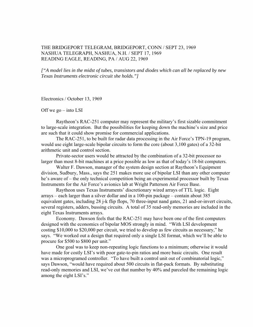
THE BRIDGEPORT TELEGRAM, BRIDGEPORT, CONN / SEPT 23, 1969 NASHUA TELEGRAPH, NASHUA, N.H. / SEPT 17, 1969 READING EAGLE, READING, PA / AUG 22, 1969 [“A model lies in the midst of tubes, transistors and diodes which can all be replaced by new Texas Instruments electronic circuit she holds.”] Electronics / October 13, 1969 Off we go – into LSI Raytheon’s RAC-251 computer may represent the military’s first sizable commitment to large-scale integration. But the possibilities for keeping down the machine’s size and price are such that it could show promise for commercial applications. The RAC-251, to be built for radar data processing in the Air Force’s TPN-19 program, would use eight large-scale bipolar circuits to form the core (about 3,100 gates) of a 32-bit arithmetic unit and control section. Private-sector users would be attracted by the combination of a 32-bit processor no larger than most 8-bit machines at a price possible as low as that of today’s 18-bit computers. Walter F. Dawson, manager of the system design section at Raytheon’s Equipment division, Sudbury, Mass., says the 251 makes more use of bipolar LSI than any other computer he’s aware of – the only technical competition being an experimental processor built by Texas Instruments for the Air Force’s avionics lab at Wright Patterson Air Force Base. Raytheon uses Texas Instruments’ discretionary wired arrays of TTL logic. Eight arrays – each larger than a silver dollar and in a 100-pin package – contain about 385 equivalent gates, including 28 j-k flip flops, 70 three-input nand gates, 21 and-or-invert circuits, several registers, adders, bussing circuits. A total of 35 read-only memories are included in the eight Texas Instruments arrays. Economy. Dawson feels that the RAC-251 may have been one of the first computers designed with the economics of bipolar MOS strongly in mind. “With LSI development costing $10,000 to $20,000 per circuit, we tried to develop as few circuits as necessary,” he says. “We worked out a design that required only a single LSI format, which we’ll be able to procure for $500 to $800 per unit.” One goal was to keep non-repeating logic functions to a minimum; otherwise it would have made for costly LSI’s with poor gate-to-pin ratios and more basic circuits. One result was a microprogramed controller. “To have built a control unit out of combinatorial logic,” says Dawson, “would have required about 500 circuits in flat-pack formats. By substituting read-only memories and LSI, we’ve cut that number by 40% and parceled the remaining logic among the eight LSI’s.”
Smaller IC’s still are necessary, he adds, because some functions just don’t repeat often enough to make LSI economical. Thus there are 17 printed-circuit cards, each measuring five by seven inches, containing ordinary integrated circuits. Much of the development of the RAC-251 came from the RAC-250, an in-house development program, during 1968 and 1969. The TI arrays used in the 250 had only about 300 equivalent gates, “but TI’s yields kept going up, and their process began to look much more repeatable as time passed,” says Dawson. “So we changed the metallization to add bussing and some other features to the LSI’s and improve our economics.” TI, he says, has never had LSI delivery problems. Two preproduction models of the RAC-251 are assembled now. They should go into checkout very soon, and should be operating by years’ end. By the final quarter of 1970, Raytheon should begin producing the 251 in enough quantity to soak up 1,000 arrays or more by 1972. Dawson already has done some thinking about the 251’s commercial possibilities. “The 251 could cost only about $20,000 if produced at 100 to 200 units a year,” he says.
Texas Instruments Reference Accession 1987.0487 Archive Center No. 697 LITERAL TRANSCRIPTION – Sparky Terry, SI Volunteer – CHIP COLLECTION