constructing a simple processor
TRANSCRIPT

Constructing a
Simple Processor
FALL 2010 – COMPUTER ARCHITECTURE I
INSTRUCTOR: MITCHELL D. THEYS

- - -
single bit 4:1 multiplexer is composed of 2 pieces: a 2-to-4 line decoder and a 4x2 AND-OR. In order
to describe the functionality of a single bit 4-to-1 multiplexer, we must show the functionality of the 2
pieces.
2-To-4 Line Decoder
Schematic of a 2-to-4 line decoder
The general definition of a decoder is converting an n bit input in order to produce an m bit output. An n
bit input can represent 2n distinct elements, with n ≤ m ≤ 2n. For a 2-to-4 line decoder, n = 2 and m = 4
which means this particular decoder can represent 22 = 4 distinct elements. There are two inputs: S0 and
S1, and four outputs: D0, D1, D2, and D3.
Each output can be described with a unique equation:

We can produce a waveform that simulates each possible input combination on our circuit. Cyan blocks
represent undefined states.
Waveform for a 2-to-4 line decoder
To check that our circuit (and waveform) is correct is, we can construct a truth table for each of the
possible input and output combinations:
S0 S1 D0 D1 D2 D3
0 0 1 0 0 0
0 1 0 1 0 0
1 0 0 0 1 0
1 1 0 0 0 1
Inputs Outputs
Truth table for a 2-to-4 line decoder
A 2-to-4 line decoder has a gate input cost.
Gate Input Cost = 2 ( 1 gates) + 4 ( 2 gates) = 2 + 8 = 10
Although the design of a 2-to-4 line decoder is relatively small, we can create an alternative sub-design
symbol for it. Throughout this report, a 2-to-4 line decoder will be illustrated with the following symbol:
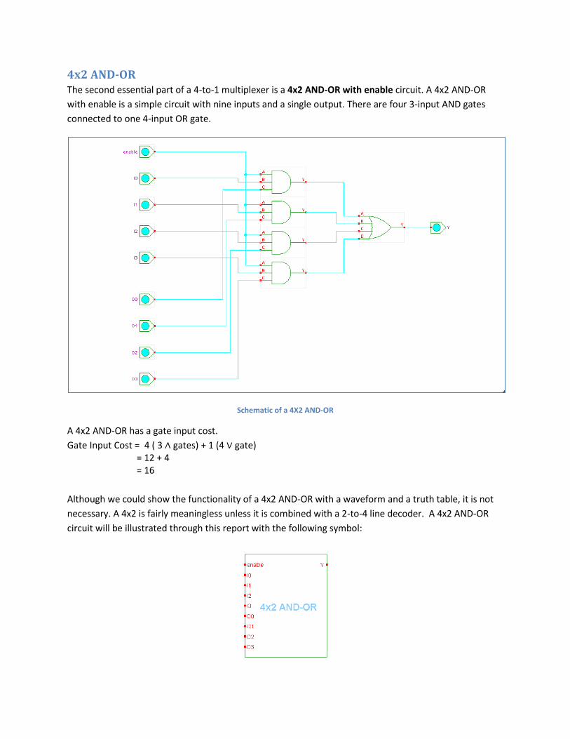
4x2 AND-OR The second essential part of a 4-to-1 multiplexer is a 4x2 AND-OR with enable circuit. A 4x2 AND-OR
with enable is a simple circuit with nine inputs and a single output. There are four 3-input AND gates
connected to one 4-input OR gate.
Schematic of a 4X2 AND-OR
A 4x2 AND-OR has a gate input cost.
Gate Input Cost = 4 ( 3 gates) + 1 (4 gate) = 12 + 4 = 16
Although we could show the functionality of a 4x2 AND-OR with a waveform and a truth table, it is not
necessary. A 4x2 is fairly meaningless unless it is combined with a 2-to-4 line decoder. A 4x2 AND-OR
circuit will be illustrated through this report with the following symbol:

Single Bit 4-To-1 Multiplexer When a 4x2 AND-OR with enable is combined with a 2-to-4 line decoder, we can create a 4-to-1
multiplexer. A 4-to-1 multiplexer has a total of 7 inputs: An enable bit, S0 and S1 represent the selector
bits, while I0, I1, I2, I3 represent the inputs to the 4x2 AND-OR circuit. A 4-to-1 multiplexer has a single
output, Y.
Schematic of a single bit 4-to-1 multiplexer
The enable input acts as an on and off switch for the circuit. When enable = 0, other input values (S0 and
S1) are unable to pass any values through the circuit, causing Y = 0. When enable = 1, S0 and S1 are
allowed to pass values through the circuit. If we wanted to represent each possible input combination
for this circuit, our truth table would require 27 = 128 lines. Instead, a condensed truth table can be
constructed for a 4-to-1 multiplexer. The X’s represent “don’t cares”; regardless of what S0 and S1 values
are, the output will always be 0:
Outputs
enable S1 S0 Y
0 X X 0
1 0 0 I0
1 0 1 I1
1 1 0 I2
1 1 1 I3
Inputs
Truth table for a 4-to-1 multiplexer

We can also produce a product-of-sums equation for a 4-to-1 multiplexer:
A waveform can allow us to interpret the behavior of a single bit 4-to-1 multiplexer. For this waveform,
I0 and I2, have been preset to 0, I1 and I3 and have been preset to be 1. The cyan blocks are undefined
states. By interpreting the waveform, we can conclude that the waveform and the truth table are
identical.
Waveform for a 4-to-1 multiplexer
A 4-to-1 multiplexer has a gate input cost.
Gate Input Cost = (2-to-4 line decoder gate input cost) + (4x2 AND-OR gate input cost) = 10 + 16 = 26

8-Bit 4-To-1 Multiplexer An 8-bit 4-to-1 multiplexer has a total of seven inputs: An enable bit, S0 and S1 represent the selector
bits to the 2-to-4 line decoder, while A8, B8, C8, D8 represent the inputs to eight 4x2 AND-OR circuits. An
8-bit 4-to-1 multiplexer has a single output, Y8. An 8-bit 4-to-1 multiplexer operates quite similarly to a
single bit 4-to-1 multiplexer. To illustrate the similarities between the two circuits, we can demonstrate
a few examples.
Verification Four test cases will be presented in this section to show the functionality of an 8-bit 4-to-1 multiplexer.
Test Case 1
8-bit 4-to-1 multiplexer, where Y = A8 = 6
In the above diagram, the enable input is active. Inputs A8 and B8 are located in the top left corner of the
diagram, while C8 and D8 are located near the bottom left corner of the diagram. When S0 and S1 are set
to 0, the value of A8 = 6 propagates through the eight 4x2 AND-OR circuits and is delivered to the output
bit Y.

Test Case 2
8-bit 4-to-1 multiplexer, where Y = B8 = 47
The enable input is active. When S0 = 1 and S1 = 0, the value of B8 = 47 propagates through the eight 4x2
AND-OR circuits and is delivered to the output bit Y.

Test Case 3
8-bit 4-to-1 multiplexer, where Y = C8 = 102
The enable input is active. When S0 = 0 and S1 = 1, the value of C8 = 102 propagates through the eight
4x2 AND-OR circuits and is delivered to the output bit Y.

Test Case 4
8-bit 4-to-1 multiplexer, where Y = D8 = 233
The enable input is active. When S0 and S1 are both equal to 1, the value of D8 = 233 propagates through
the eight 4x2 AND-OR circuits and is delivered to the output bit Y.
An 8-bit 4-to-1 multiplexer has a gate input cost.
Gate Input Cost = 1 (2-to-4 line decoder gate input cost) + 8(4x2 AND-OR gate input cost) = 10 + 8(16) = 10 + 128 = 138
A final waveform illustrating these test cases is shown below:
Waveform of an 8-bit 4-to-1 multiplexer
-
efore assembling an 8-bit full adder, we must first construct a single bit full adder.
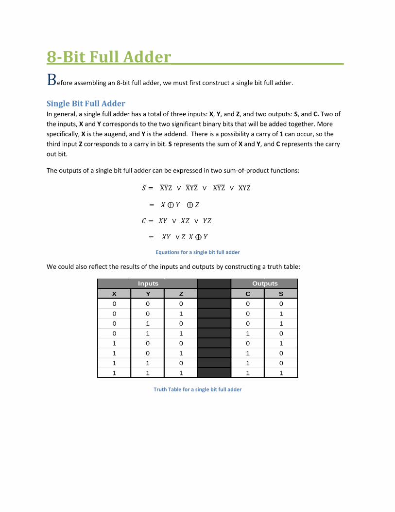
Single Bit Full Adder In general, a single full adder has a total of three inputs: X, Y, and Z, and two outputs: S, and C. Two of
the inputs, X and Y corresponds to the two significant binary bits that will be added together. More
specifically, X is the augend, and Y is the addend. There is a possibility a carry of 1 can occur, so the
third input Z corresponds to a carry in bit. S represents the sum of X and Y, and C represents the carry
out bit.
The outputs of a single bit full adder can be expressed in two sum-of-product functions:
Equations for a single bit full adder
We could also reflect the results of the inputs and outputs by constructing a truth table:
X Y Z C S
0 0 0 0 0
0 0 1 0 1
0 1 0 0 1
0 1 1 1 0
1 0 0 0 1
1 0 1 1 0
1 1 0 1 0
1 1 1 1 1
Inputs Outputs
Truth Table for a single bit full adder
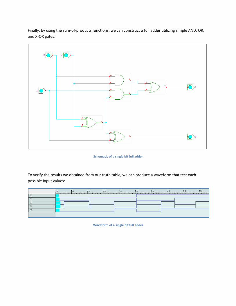
Finally, by using the sum-of-products functions, we can construct a full adder utilizing simple AND, OR,
and X-OR gates:
Schematic of a single bit full adder
To verify the results we obtained from our truth table, we can produce a waveform that test each
possible input values:
Waveform of a single bit full adder

We interpret our waveform by observing how the values of the inputs produce outputs. Cyan blocks on
the waveform represent undefined states.
Interval
X Y Z C S
0 0 0 0 0 0.3-0.5
0 0 1 0 1 0.5-2.1
0 1 0 0 1 2.1-3.6
0 1 1 1 0 3.6-5.05
1 0 0 0 1 5.05-6.6
1 0 1 1 0 6.6-7.4
1 1 0 1 0 7.4-8.7
1 1 1 1 1 8.7-9.6
Inputs Outputs
Waveform input and output values with time intervals.
The truth table and the outcomes in the waveform show that the two are equivalent.
A single bit full adder also has a gate input cost.
Gate Input Cost = 2 ( 2 gates) + 2 ( 2 gates) + 1 ( 2 gates) = 4 + 4 + 2 = 10
The symbol for a full adder is shown below:
8-Bit Ripple Carry Adder Ripple carry adders are beneficial, because they allow the computer to perform simple arithmetic sums.
A ripple carry adder uses n consecutive full adders, with each input bit producing a sum. Full adders are
connected to one another by their Z input (carry in) and C output (carry out). If a carry of 1 occurs in the
least significant bit, its value propagates to the next full adder, and so on. For an 8-bit ripple carry adder,
n = 8.

Schematic of an 8-bit full adder
The design of an 8-bit full adder is rather complex. There are three inputs: X8, Y8 and Z, and two
outputs: S8 and C. The inputs and outputs still have similar definitions as those presented in a single bit
full adder. However, X8, Y8, and S8 are 8-bit values. Each full adder is placed in a specific position, such
that full adder 0 is placed in the least significant bit position and full adder 7 is place in the most
significant bit position.
Since we previously understand how a single bit full adder operates, we are not required to produce a
truth table for an 8-bit full adder. If we wanted to set up a truth table we will need 216 = 65,536 lines.
Not only is 65,536 lines a great deal of information, half of it is unnecessary because of repetition.
Instead, we can use the information we introduced earlier to show that our 8-bit full adder is functional.

Verification Seven test cases will be presented in this section to show the functionality of an 8-bit full adder.
Test Case 1
Illustrating 1 + 1 = 2
In this example, X = 1 and Y = 1. When we add X + Y, a carry of 1 occurs in Full Adder 0. When this
occurs, the 1 propagates into full adder 1. Since Full Adder 0 and Full Adder 1 are both structured the
same way, Full Adder 1 will simply process the carry in value as if it were a single full adder. Once the
addition is complete, and no other carry in’s occur, the output value is delivered to the S output pin. The
result of X + Y = 2.

Test Case 2
Illustrating 11 + 1 = 12
In this example, X = 11 and Y = 1. When we add X + Y, a carry of 1 occurs in Full Adder 0. When this
occurs, the 1 propagates into Full Adder 1. Another carry of 1 occurs in Full Adder 1, and similarly,
propagates to Full Adder 2. Full Adder 0, Full Adder 1, Full Adder 2 are both structured the same way,
Full Adder 2 will simply process the carry in value as if it were a single full adder. Once the addition is
complete, and no other carry in’s occur, the output value is delivered to the S output pin. The result of X
+ Y = 12.

Test Case 3
Illustrating 23 + 7 = 30
In this example, X =23 and Y = 7. Like the previous two examples, the same pattern holds. When we add
X + Y, a carry of 1 occurs in Full Adder 0. When this occurs, the 1 propagates into Full Adder 1. Another
carry of 1 occurs in Full Adder 1, and similarly, propagates to Full Adder 2. A final carry of 1 occurs in Full
Adder 2, and is propagated into Full Adder 3. Once the addition is complete, and no other carry in’s
occur, the output value is delivered to the S output pin. The result of X + Y = 30.

Test Case 4
Illustrating 11 + 5 = 16
In this example, X =11 and Y = 5. Like the previous three examples, the same pattern holds. When we
add X + Y, a carry of 1 occurs in Full Adder 0, and is carried into Full Adder 1. Another carry of 1 occurs in
Full Adder 1, and is carried into to Full Adder 2. Another carry of 1 occurs in Full Adder 2, and is carried
into Full Adder 3. A final carry of 1 occurs in Full Adder 3, and is carried into Full Adder 4. Once the
addition is complete, and no other carry in’s occur, the output value is delivered to the S output pin. The
result of X + Y = 16.

Test Case 5
Illustrating 23 + 9 = 32
In this example, X =23 and Y = 9. A carry in of 1 occurs in Full Adder 0 and propagates from Full Adder 0
to Full Adder 5. Once the addition is complete, and no other carry in’s occur, the output value is
delivered to the S output pin. The result of X + Y = 32.

Test Case 6
Illustrating 55 + 9 = 64
In this example, X =55 and Y = 9. Like the previous examples, the same pattern holds. A carry in of 1
occurs in Full Adder 0 and propagates from Full Adder 0 to Full Adder 6. Once the addition is complete,
and no other carry in’s occur, the output value is delivered to the S output pin. The result of X + Y = 64.

Test Case 7
Illustrating 255 + 255 = 510
In this example, X =255 and Y = 255. Like the previous examples, the same pattern holds. A carry in of 1
occurs in Full Adder 0 and propagates from Full Adder 0 to Full Adder 7. However, another carry of 1
occurs in Full Adder 7, and its value is delivered to C. There simply isn’t enough bit position available in
S, and an overflow occurs. The result of X + Y = 510.
Gate Input Cost = 8 (1 Single Bit Full Adder) = 8 (10) = 80
A final waveform illustrating these test cases is shown below, along with each occurrence of the carry
out values for each Full Adder:
Waveform of an 8-bit full adder