concept of plasmonic waveguide inspired by half … very compact as its width extends only over a...
TRANSCRIPT
Concept of Plasmonic Waveguide Inspired by Half-ModeSubstrate-Integrated Waveguide
Dirk Baumann∗, Christophe Fumeaux†, Withawat Withayachumnankul†, Rudiger Vahldieck∗∗Laboratory for Electromagnetic Fields and Microwave Electronics, ETH Zurich, 8092 Zurich, Switzerland†School of Electrical and Electronic Engineering, The University of Adelaide, Adelaide 5005, Australia
Email: [email protected], [email protected]
Abstract— A new concept of a plasmonic waveguide foroptical frequencies is introduced. The waveguide is inspiredby the half-mode substrate-integrated waveguide (HMSIW),which is in use in the microwave regime. The design of theplasmonic HMSIW however requires to take into accountthe particularities of the materials in the optical regime,which leads to modified design rules compared to microwavefrequencies. It is shown that the proposed nanoscale plas-monic HMSIW is able to guide electromagnetic waves overa short distance while being characterized by very compactsize. The design parameters found in this paper are derivedfrom electromagnetic simulations based on the Finite-VolumeTime-Domain (FVTD) method.
Index Terms— Plasmonics, SPP, HMSIW, FVTD.
I. INTRODUCTION
Guiding electromagnetic waves at optical frequenciesin the nanoscale regime is a challenging task because ofthe diffraction limit. However, in order to build nanoscale-optical waveguides, this limit can be circumvented byemploying surface plasmon polaritons (SPPs) that can beexcited at an interface between dielectrics and metals [1].Metals, such as gold or silver, can support SPPs at opticalfrequencies owing to their appropriate complex permittiv-ity, i.e. a negative real part and a small absolute imagi-nary part. These SPPs can be exploited to guide wavesalong dielectric-metal interfaces, taking advantage of thesubwavelength confinement of electromagnetic waves [2].
In this paper, a new concept of an optical plasmonicwaveguide is introduced. This concept is inspired by thehalf-mode substrate integrated waveguide (HMSIW) [3],which is scaled and adapted to be manufacturable andoperable at optical frequencies. This plasmonic HMSIWis very compact as its width extends only over a smallfraction of the excitation wavelength while it is able toguide electromagnetic waves over a distance equivalentto a few wavelengths. At this early stage, the basicoperation of the waveguide is investigated through ananalysis of its propagation constant, realized using 3Dfull-wave electromagnetic simulations. This is especiallychallenging because of the dispersive nature of metal atoptical frequencies and because of the thin dielectric layer,sandwiched in between thicker gold layers. The vicinityof the dielectric-gold interface in the guide requires avery fine discretization in order to capture the propagating
mode. Such a structure can be efficiently modeled withan unstructured grid, where the size of the elements canquickly grow within a few grid layers. A method which hasbeen shown to successfully model plasmonic structures isthe Finite-Volume Time-Domain (FVTD) method [4], [5].
After a brief introduction of the FVTD method, the basicdesign of the plasmonic HMSIW is presented. Principledesign rules for an optimal operation of the waveguideare deduced from its FVTD analysis, and the difference tothe microwave version are highlighted.
II. SIMULATION METHOD: FVTD
Since the end of the 1980s, the FVTD method is suc-cessfully applied in computational electromagnetics. Themethod is especially well suited for multi-scale problems.Its explicit time-stepping scheme results in linear memorygrowth and at the same time the application in an unstruc-tured, tetrahedral mesh provides the means to minimizethe overall number of elements required for discretizingmulti-scale problems. Additionally, a geometry-matchedlocal-time stepping scheme provides a further reductionof the CPU time, commonly around a factor of 3 to5 [6]. For long structures, such as waveguides, a conformalPML facilitates the size minimization of the computationaldomain while keeping the unintended reflections from theboundary at the same level as spherical PMLs [7].
III. DESIGN OF PLASMONIC HMSIW
The concept of a substrate-integrated waveguide (SIW)surfaced in 2001 in order to simplify the transition from amicrostrip line to a rectangular waveguide [8]. Tradition-ally, the SIW side walls are realized as a row of vias. Fiveyears later, a further size reduction was achieved with thehalf-mode substrate integrated waveguide (HMSIW) [9],[3]. In this paper, the concept of a HMSIW is scaled andadapted to optical frequencies resulting in the design ofa compact nanoscale waveguide. The principle design ofthis plasmonic HMSIW is shown in Fig. 1. Its dimensionsand materials are consistent with standard capabilitiesof modern nano-fabrication techniques. Similarly to theconventional HMSIW, a layer of conductor (gold [10]) ispartly surrounding a very thin dielectric SiO2 (εr = 2.31)layer. This constitutes one half of a rectangular waveguide
978-1-4673-1088-8/12/$31.00 ©2012 IEEE

Au
SiO2
dw
hd
d
substrate
plasmonic
HMSIW
Fig. 1. Profile and dimensions of the plasmonic waveguide.
with height h and width w, where a half quasi-TE10 modecan propagate. As an important difference to a scaledmicrowave counterpart, the optical electromagnetic field ispenetrating significantly into the gold because of a smallnegative permittivity. Therefore, the waveguide walls haveto have a certain thickness in order to permit the plasmonicmode to build and propagate. Here the thickness is chosenas d = 40 nm. The plasmonic HMSIW is modeled in
0
-20
-40
-80
-100200 250 300 350 400 500450
-60
Pe
rmit
tiv
ity
Frequency (THz)
real
imaginary
Fig. 2. Complex permittivity of gold in between 200 and 500 THz [4].
ABC
SiOsubstrate
2
Port
PML
z
y
x
Au
SiO2
Mesh
Fig. 3. Open view of the FVTD model of the plasmonic HMSIW. Theinsets show the port and the fine mesh employed at the waveguide region.
FVTD according to the geometry described above, withwaveguide height h = 5 nm, various widths in betweenw = 10 . . . 80 nm, and with a length of L = 1.5µm.The dispersive characteristic of gold, as plotted in Fig. 2,is approximated with a double-Lorentz single-Drude polemodel, with parameters as in [4]. In order to capture theplasmonic effects of the waveguide, the SiO2 inside thewaveguide and the surrounding gold layer are discretized
with a maximal linear cell size of 2 nm. This set-up resultsin a total of 4 to 7 million tetrahedral cells. An openview of the FVTD model is shown in Fig. 3. In theFVTD simulation, the mode in the guide is excited ashalf the TE10 mode of a perfect rectangular waveguide.A conformal PML boundary condition is applied on thecylindrical outer computational boundary.
IV. RESULTS
The propagation constant γ = α+jβ is determined fromthe FVTD simulations. The phase constant β is evaluatedbased on the guided wavelength λg which is measuredby the average distance between two maxima of thepropagating wave inside the waveguide. The attenuationconstant α is determined by considering two points atdistance z1 and z2 from the source in the guide
α = (z2 − z1)−1 · ln |Ex(z1)/Ex(z2)| . (1)
For the analysis points z1 and z2 are chosen at a distancefrom the waveguide ends to avoid any detrimental effectsfrom the source and from the absorbing termination.
100 nm PML
PML
PMLw = 80nm
w = 20nm
w = 35nm
Fig. 4. Capped amplitude of the electric field at 300THz inside thewaveguide.
As an illustrating example, Fig. 4 shows the electric fieldamplitude at f = 300THz inside a plasmonic HMSIWwith SiO2 layer height h = 5 nm. For a width of w =20 nm, the mode is below cut-off, whereas for w = 35 nmand w = 80 nm the mode is propagating.
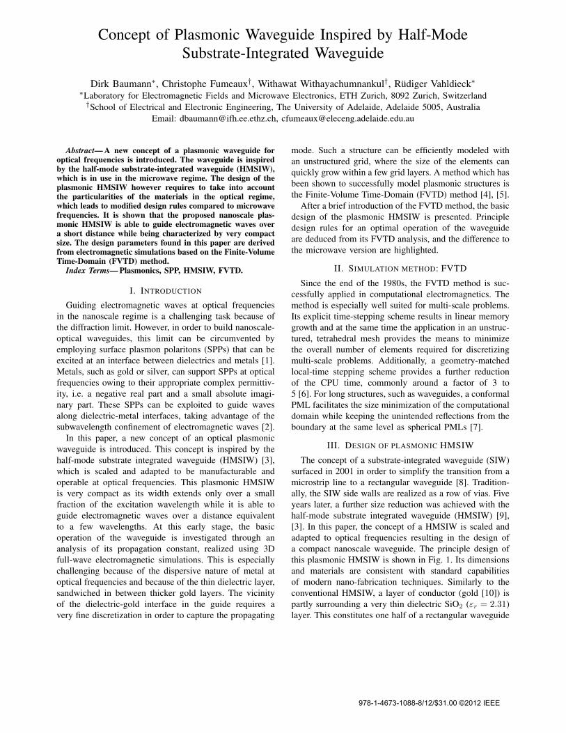
The phase constant for waveguides with height h =5 nm and different widths w is plotted in Fig. 5. The cut-off frequency is clearly observed in this frequency rangefor w = 15 nm, 20 nm and 35 nm showing that therecan be only propagation for frequencies above the width-dependent cut-off.
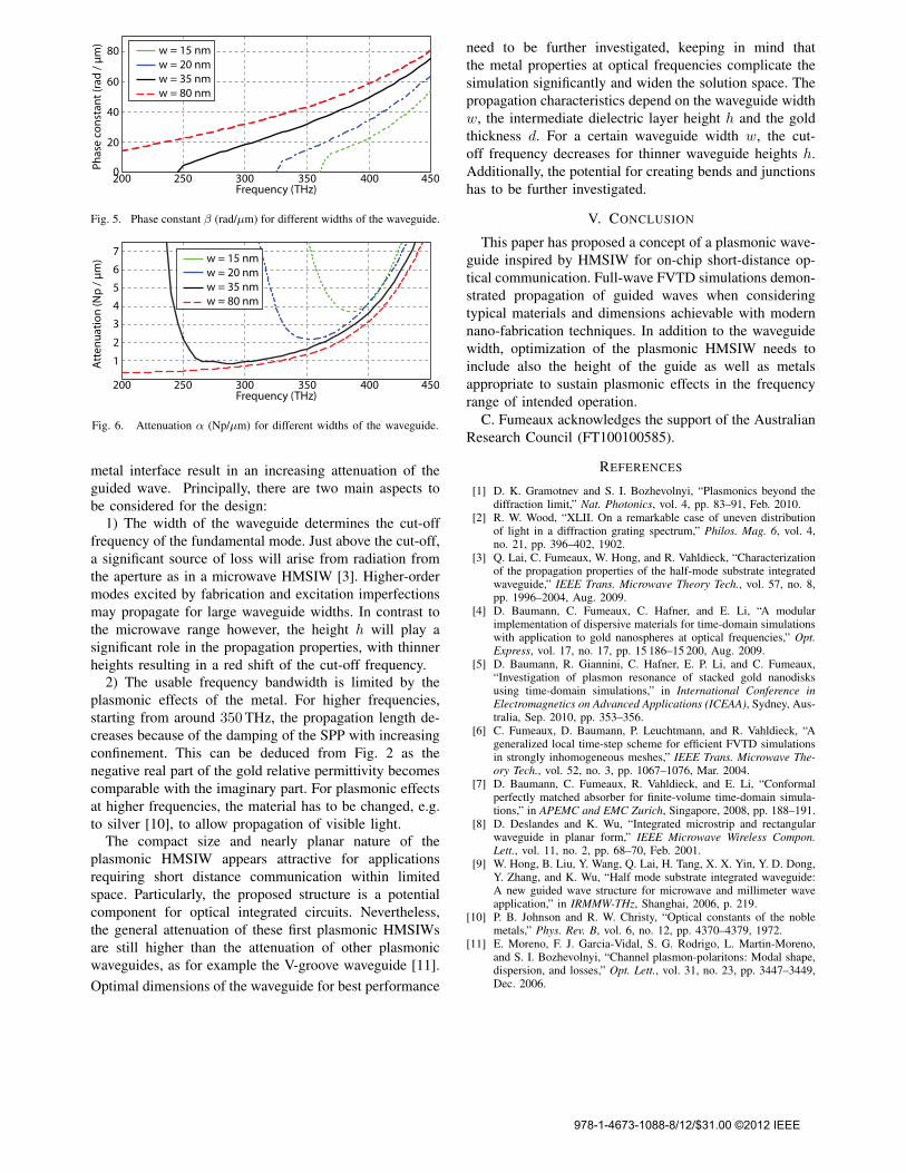
The attenuation constant is plotted in Fig. 6. For w =15 nm, 20 nm and 35 nm, as the propagating mode justabove cut-off is a fast wave, radiation losses from theaperture are observed as strong attenuation which de-creases very quickly with increasing frequency. For allwaveguide widths, above a frequency of approximately350THz, the SPPs confinement properties at the dielectric
978-1-4673-1088-8/12/$31.00 ©2012 IEEE
w = 15 nm
w = 20 nm
w = 35 nm
w = 80 nm
80
60
40
20
0
Ph
ase
co
nst
an
t (r
ad
/ μ
m)
200 250 300 350 400 450Frequency (THz)
Fig. 5. Phase constant β (rad/µm) for different widths of the waveguide.
7
6
5
3
4
1
2
Att
en
ua
tio
n (
Np
/ μ
m)
200 250 300 350 400 450Frequency (THz)
w = 15 nm
w = 20 nm
w = 35 nm
w = 80 nm
Fig. 6. Attenuation α (Np/µm) for different widths of the waveguide.
metal interface result in an increasing attenuation of theguided wave. Principally, there are two main aspects tobe considered for the design:
1) The width of the waveguide determines the cut-offfrequency of the fundamental mode. Just above the cut-off,a significant source of loss will arise from radiation fromthe aperture as in a microwave HMSIW [3]. Higher-ordermodes excited by fabrication and excitation imperfectionsmay propagate for large waveguide widths. In contrast tothe microwave range however, the height h will play asignificant role in the propagation properties, with thinnerheights resulting in a red shift of the cut-off frequency.
2) The usable frequency bandwidth is limited by theplasmonic effects of the metal. For higher frequencies,starting from around 350THz, the propagation length de-creases because of the damping of the SPP with increasingconfinement. This can be deduced from Fig. 2 as thenegative real part of the gold relative permittivity becomescomparable with the imaginary part. For plasmonic effectsat higher frequencies, the material has to be changed, e.g.to silver [10], to allow propagation of visible light.
The compact size and nearly planar nature of theplasmonic HMSIW appears attractive for applicationsrequiring short distance communication within limitedspace. Particularly, the proposed structure is a potentialcomponent for optical integrated circuits. Nevertheless,the general attenuation of these first plasmonic HMSIWsare still higher than the attenuation of other plasmonicwaveguides, as for example the V-groove waveguide [11].Optimal dimensions of the waveguide for best performance
need to be further investigated, keeping in mind thatthe metal properties at optical frequencies complicate thesimulation significantly and widen the solution space. Thepropagation characteristics depend on the waveguide widthw, the intermediate dielectric layer height h and the goldthickness d. For a certain waveguide width w, the cut-off frequency decreases for thinner waveguide heights h.Additionally, the potential for creating bends and junctionshas to be further investigated.
V. CONCLUSION
This paper has proposed a concept of a plasmonic wave-guide inspired by HMSIW for on-chip short-distance op-tical communication. Full-wave FVTD simulations demon-strated propagation of guided waves when consideringtypical materials and dimensions achievable with modernnano-fabrication techniques. In addition to the waveguidewidth, optimization of the plasmonic HMSIW needs toinclude also the height of the guide as well as metalsappropriate to sustain plasmonic effects in the frequencyrange of intended operation.
C. Fumeaux acknowledges the support of the AustralianResearch Council (FT100100585).
REFERENCES
[1] D. K. Gramotnev and S. I. Bozhevolnyi, “Plasmonics beyond thediffraction limit,” Nat. Photonics, vol. 4, pp. 83–91, Feb. 2010.
[2] R. W. Wood, “XLII. On a remarkable case of uneven distributionof light in a diffraction grating spectrum,” Philos. Mag. 6, vol. 4,no. 21, pp. 396–402, 1902.
[3] Q. Lai, C. Fumeaux, W. Hong, and R. Vahldieck, “Characterizationof the propagation properties of the half-mode substrate integratedwaveguide,” IEEE Trans. Microwave Theory Tech., vol. 57, no. 8,pp. 1996–2004, Aug. 2009.
[4] D. Baumann, C. Fumeaux, C. Hafner, and E. Li, “A modularimplementation of dispersive materials for time-domain simulationswith application to gold nanospheres at optical frequencies,” Opt.Express, vol. 17, no. 17, pp. 15 186–15 200, Aug. 2009.
[5] D. Baumann, R. Giannini, C. Hafner, E. P. Li, and C. Fumeaux,“Investigation of plasmon resonance of stacked gold nanodisksusing time-domain simulations,” in International Conference inElectromagnetics on Advanced Applications (ICEAA), Sydney, Aus-tralia, Sep. 2010, pp. 353–356.
[6] C. Fumeaux, D. Baumann, P. Leuchtmann, and R. Vahldieck, “Ageneralized local time-step scheme for efficient FVTD simulationsin strongly inhomogeneous meshes,” IEEE Trans. Microwave The-ory Tech., vol. 52, no. 3, pp. 1067–1076, Mar. 2004.
[7] D. Baumann, C. Fumeaux, R. Vahldieck, and E. Li, “Conformalperfectly matched absorber for finite-volume time-domain simula-tions,” in APEMC and EMC Zurich, Singapore, 2008, pp. 188–191.
[8] D. Deslandes and K. Wu, “Integrated microstrip and rectangularwaveguide in planar form,” IEEE Microwave Wireless Compon.Lett., vol. 11, no. 2, pp. 68–70, Feb. 2001.
[9] W. Hong, B. Liu, Y. Wang, Q. Lai, H. Tang, X. X. Yin, Y. D. Dong,Y. Zhang, and K. Wu, “Half mode substrate integrated waveguide:A new guided wave structure for microwave and millimeter waveapplication,” in IRMMW-THz, Shanghai, 2006, p. 219.
[10] P. B. Johnson and R. W. Christy, “Optical constants of the noblemetals,” Phys. Rev. B, vol. 6, no. 12, pp. 4370–4379, 1972.
[11] E. Moreno, F. J. Garcia-Vidal, S. G. Rodrigo, L. Martin-Moreno,and S. I. Bozhevolnyi, “Channel plasmon-polaritons: Modal shape,dispersion, and losses,” Opt. Lett., vol. 31, no. 23, pp. 3447–3449,Dec. 2006.
978-1-4673-1088-8/12/$31.00 ©2012 IEEE