comx communication modules - hilscher.com...design guide comx communication modules hilscher...
TRANSCRIPT
Design Guide COMX Communication Modules
Hilscher Gesellschaft für Systemautomation mbH www.hilscher.com
DOC100901DG21EN | Revision 21 | English | 2015-11 | Released | Public
Introduction 2/79
COMX Communication Modules | Design Guide DOC100901DG21EN | Revision 21 | English | 2015-11 | Released | Public © Hilscher, 2002-2015
Table of Contents 1 Introduction.............................................................................................................................................4
1.1 About this document ......................................................................................................................4 1.2 Comparison COMX and COM modules.........................................................................................5 1.3 List of revisions ..............................................................................................................................6 1.4 Technical features..........................................................................................................................7 1.5 Module names................................................................................................................................9 1.6 References to documents ............................................................................................................10 1.7 Legal notes...................................................................................................................................11
1.7.1 Copyright ......................................................................................................................................... 11 1.7.2 Important notes ............................................................................................................................... 11 1.7.3 Exclusion of liability ......................................................................................................................... 12 1.7.4 Warranty.......................................................................................................................................... 12 1.7.5 Export regulations ........................................................................................................................... 12
2 Design-in - Mechanical aspects..........................................................................................................13 2.1 Type of COMX modules...............................................................................................................13 2.2 Mechanical dimensions................................................................................................................15
2.2.1 Common mechanical dimensions for COMX modules .................................................................... 15 2.2.2 Mechanical dimensions of COMX modules ..................................................................................... 15
2.3 Type of connector ........................................................................................................................25 2.3.1 Storage and contact reliability of host-side connector ..................................................................... 27
2.4 Mounting of COMX modules........................................................................................................28 2.5 Material recommendation for the faceplate..................................................................................34 2.6 Designation of the COMX module ...............................................................................................34 2.7 Meaning of the address switch ....................................................................................................34
2.7.1 PROFIBUS DP Slave ...................................................................................................................... 34 2.7.2 CANopen Slave............................................................................................................................... 35 2.7.3 DeviceNet Slave.............................................................................................................................. 35 2.7.4 CC-Link Slave ................................................................................................................................. 36
2.7.4.1 COMX 10CA-CCS and COMX 10CN-CCS....................................................................... 36 2.7.4.2 COMX 50CA-CCS ............................................................................................................ 37
3 Design-in - Electrical aspects .............................................................................................................39 3.1 Host interface ...............................................................................................................................39
3.1.1 Host interface overview: Dual-port memory sizes and modes......................................................... 39 3.1.2 Host interface: Parallel or serial dual-port memory mode................................................................ 40
3.1.2.1 COMX 50 and COMX 100 ................................................................................................ 40 3.1.2.2 COMX 10 and COMX 51 .................................................................................................. 40
3.1.3 COMX pin assignment of the system bus connector X1 Parallel mode........................................ 42 3.1.4 COMX pin assignment of the system bus connector X1 Serial mode .......................................... 44 3.1.5 PAD type explanation ...................................................................................................................... 45 3.1.6 Signal overview and pin assignment of the fieldbus connector X2 on COMX CN ........................... 47
3.1.6.1 Fieldbus connector X2 for CC-Link Slave ......................................................................... 47 3.1.6.2 Fieldbus Connector X2 for CANopen-Master/-Slave ........................................................ 48 3.1.6.3 Fieldbus Connector X2 for DeviceNet-Master/-Slave ....................................................... 49 3.1.6.4 Fieldbus Connector X2 for PROFIBUS-Master/-Slave...................................................... 50 3.1.6.5 Fieldbus Connector X2 for Real Time Ethernet ................................................................ 51
3.1.7 Common signals of the host interface ............................................................................................. 53 3.1.7.1 Power supply of the COMX modules ................................................................................ 53 3.1.7.2 RESET signal ................................................................................................................... 53
3.1.8 Signals of the host interface Parallel dual-port memory mode ..................................................... 53 3.1.8.1 The dual-port memory bus of COMX ................................................................................ 53 3.1.8.2 Address Bus and Data Bus............................................................................................... 54 3.1.8.3 Dual-Port Memory Control Lines....................................................................................... 54 3.1.8.4 Interrupt Line to the Host System ..................................................................................... 54 3.1.8.5 BUSY Line to the Host System......................................................................................... 55 3.1.8.6 Interfacing to the Dual-Port Memory for COMX ................................................................ 55 3.1.8.7 Timing Diagram parallel Dual-Port Memory Interface ....................................................... 56 3.1.8.8 Integration of COMX Module into a Host System ............................................................. 58
3.1.9 Signals of the host interface Serial dual-port memory mode ........................................................ 59 3.2 Fieldbus interface.........................................................................................................................60 3.3 LEDs.............................................................................................................................................61 3.4 Diagnostic interface......................................................................................................................63
3.4.1 Diagnostic interface RS232C .......................................................................................................... 63
Introduction 3/79
COMX Communication Modules | Design Guide DOC100901DG21EN | Revision 21 | English | 2015-11 | Released | Public © Hilscher, 2002-2015
3.4.2 Diagnostic interface USB................................................................................................................. 64 3.5 SYNC signals ...............................................................................................................................67
4 Technical data.......................................................................................................................................68 4.1 Product tests ................................................................................................................................70
4.1.1 COMX 10CA-CCS........................................................................................................................... 70 4.1.2 COMX 10CN-CCS........................................................................................................................... 70 4.1.3 COMX 10CA-COS........................................................................................................................... 70 4.1.4 COMX 10CN-COS .......................................................................................................................... 71 4.1.5 COMX 10CA-DPS ........................................................................................................................... 71 4.1.6 COMX 10CN-DPS........................................................................................................................... 71 4.1.7 COMX 10CA-DNS........................................................................................................................... 72 4.1.8 COMX 10CN-DNS........................................................................................................................... 72 4.1.9 COMX 50CA-REFO ........................................................................................................................ 72 4.1.10 COMX 50CA-CCS........................................................................................................................... 73 4.1.11 COMX 51CA-RE ............................................................................................................................. 73 4.1.12 COMX 51CN-RE ............................................................................................................................. 73 4.1.13 COMX 100CA-CO ........................................................................................................................... 74 4.1.14 COMX 100CA-DN ........................................................................................................................... 74 4.1.15 COMX 100CA-DP ........................................................................................................................... 74 4.1.16 COMX 100CA-RE ........................................................................................................................... 75 4.1.17 COMX 100CN-CO........................................................................................................................... 75 4.1.18 COMX 100CN-DN ........................................................................................................................... 75 4.1.19 COMX 100CN-DP ........................................................................................................................... 76 4.1.20 COMX 100CN-RE ........................................................................................................................... 76
5 Appendix ...............................................................................................................................................77 5.1 List of tables .................................................................................................................................77 5.2 List of figures................................................................................................................................78 5.3 Contacts .......................................................................................................................................79

Introduction 4/79
COMX Communication Modules | Design Guide DOC100901DG21EN | Revision 21 | English | 2015-11 | Released | Public © Hilscher, 2002-2015
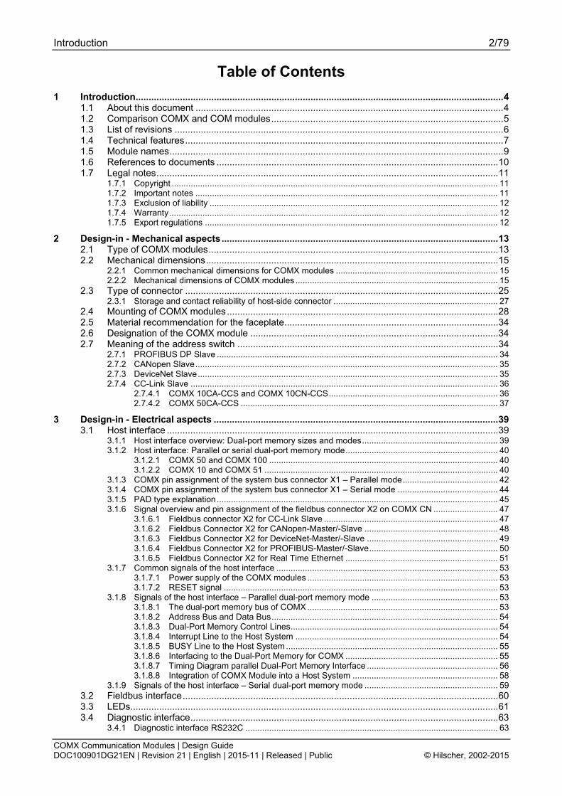
1 Introduction 1.1 About this document COMX means Communication Modules netX. These modules provide a universal and easy to use fieldbus interface for integration on various host systems. Through the set of standard application interfaces and the same board dimensions in each COMX family it is easy to switch between the different fieldbus systems, e.g. PROFIBUS DP, CANopen, DeviceNet, CC-Link or Ethernet by changing the module. This manual describes only the hardware part of the modules. The COMX communication modules is a generation of Modules and offer beside fieldbus commu-nication also Real-Time Ethernet communication. The application interface is different (not com-patible) compared to COM Modules. The application interface of the COMX Modules is common to all our COMX communication modules, and PC cards CIFX and netJACK communication modules described in our toolkit manual, dual-port memory interface manual and the Real Time Ethernet respectively fieldbus related details are defined in our Protocol API Manuals. COM Modules are the previous generation of communication modules. The COM Modules are de-scribed in an own manual. The following two tables give a comparison of both COM and COMX Modules.
Introduction 5/79
COMX Communication Modules | Design Guide DOC100901DG21EN | Revision 21 | English | 2015-11 | Released | Public © Hilscher, 2002-2015
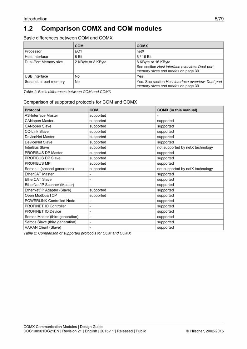
1.2 Comparison COMX and COM modules Basic differences between COM and COMX
COM COMX Processor EC1 netX Host Interface 8 Bit 8 / 16 Bit Dual-Port Memory size 2 KByte or 8 KByte 8 KByte or 16 KByte
See section Host interface overview: Dual-port memory sizes and modes on page 39.
USB Interface No Yes Serial dual-port memory No Yes. See section Host interface overview: Dual-port
memory sizes and modes on page 39. Table 1: Basic differences between COM and COMX
Comparison of supported protocols for COM and COMX
Protocol COM COMX (in this manual) AS-Interface Master supported - CANopen Master supported supported CANopen Slave supported supported CC-Link Slave supported supported DeviceNet Master supported supported DeviceNet Slave supported supported InterBus Slave supported not supported by netX technology PROFIBUS DP Master supported supported PROFIBUS DP Slave supported supported PROFIBUS MPI supported supported Sercos II (second generation) supported not supported by netX technology EtherCAT Master - supported EtherCAT Slave - supported EtherNet/IP Scanner (Master) - supported EtherNet/IP Adapter (Slave) supported supported Open Modbus/TCP supported supported POWERLINK Controlled Node - supported PROFINET IO Controller - supported PROFINET IO Device - supported Sercos Master (third generation) - supported Sercos Slave (third generation) - supported VARAN Client (Slave) - supported
Table 2: Comparison of supported protocols for COM and COMX
Introduction 6/79
COMX Communication Modules | Design Guide DOC100901DG21EN | Revision 21 | English | 2015-11 | Released | Public © Hilscher, 2002-2015
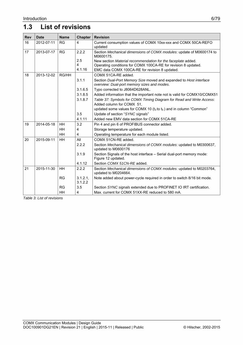
1.3 List of revisions Rev Date Name Chapter Revision 16 2012-07-11 RG 4 Current consumption values of COMX 10xx-xxx and COMX 50CA-REFO
updated 17 2013-07-17 RG 2.2.2
2.5 4 4.1.16
Section Mechanical dimensions of COMX modules: update of M0600174 to M0600175. New section Material recommendation for the faceplate added. Operating conditions for COMX 100CA-RE for revision 8 updated. EMC data COMX 100CA-RE for revision 8 updated.
18 2013-12-02 RG/HH COMX 51CA-RE added. 3.1.1 Section Dual-Port Memory Size moved and expanded to Host interface
overview: Dual-port memory sizes and modes. 3.1.6.5 Typo corrected to J8064D628ANL. 3.1.8.5 Added information that the important note not is valid for COMX10/COMX51 3.1.8.7 Table 37: Symbols for COMX Timing Diagram for Read and Write Access:
Added column for COMX 51, updated some values for COMX 10 (t3 to t5 ) and in column Common
3.5 Update of section SYNC signals 4.1.11 Added new EMV data section for COMX 51CA-RE 19 2014-05-18 HH 3.2 Pin 4 and pin 6 of PROFIBUS connector added. HH 4 Storage temperature updated. HH 4 Operating temperature for each module listed. 20 2015-09-11 HH All COMX 51CN-RE added. 2.2.2 Section Mechanical dimensions of COMX modules: updated to M0300637,
updated to M0600176 3.1.9 Section Signals of the host interface Serial dual-port memory mode:
Figure 12 updated. 4.1.12 Section COMX 51CN-RE added. 21 2015-11-30 HH 2.2.2 Section Mechanical dimensions of COMX modules: updated to M0203764,
updated to M0204664. RG 3.1.2.1,
3.1.2.2 Note added about power-cycle required in order to switch 8/16 bit mode.
RG 3.5 Section SYNC signals extended due to PROFINET IO IRT certification. HH 4 Max. current for COMX 51XX-RE reduced to 580 mA.
Table 3: List of revisions
Introduction 7/79
COMX Communication Modules | Design Guide DOC100901DG21EN | Revision 21 | English | 2015-11 | Released | Public © Hilscher, 2002-2015
1.4 Technical features Common technical features for COMX
! All leading Fieldbus and Real Time Ethernet Protocols available as Master and Slave ! One common hardware for all Real Time Ethernet Protocols ! Easy to use dual-port memory interface, with additional serial and diagnostic interface ! USB or serial diagnostic interface at COMX ! Host interface is designed for 8 KBytes (COMX 10) and for 16 KByte (COMX 50, COMX 51
and COMX 100) address space of the dual-port memory with selectable bus width of 8 or 16 bit.
! 3.3 V power supply reduces power consumption ! Small footprint for the host connector with 50 mil grid ! Solid mechanical assembly and a massive connection to earth ground by metal blocks spe-
cial design for the requirements of the modules with fieldbus connector ! Two dowels for exact mounting of the module on the host board ! Metal blocks can easily modified for special customer requirements ! Front panel can be mounted on the metal blocks that the modules have always the same
front size and covers the fieldbus connector ! Many modules are available in extended temperature specification (operating temperature
range -20°C +65°C) ! COMX 10 modules have address switches to set the bus address ! COMX 10 and COMX 51 modules offer a serial dual-port memory mode as interface to the
host
CA and CN types of COMX modules
For the COMX family, Hilscher offers modules with angled or without fieldbus connectors: ! COMX CN: COMX Modules without fieldbus respectively Ethernet connector ! COMX CA: COMX Modules with angled fieldbus, Ethernet respectively fiber optics connector
Introduction 8/79
COMX Communication Modules | Design Guide DOC100901DG21EN | Revision 21 | English | 2015-11 | Released | Public © Hilscher, 2002-2015
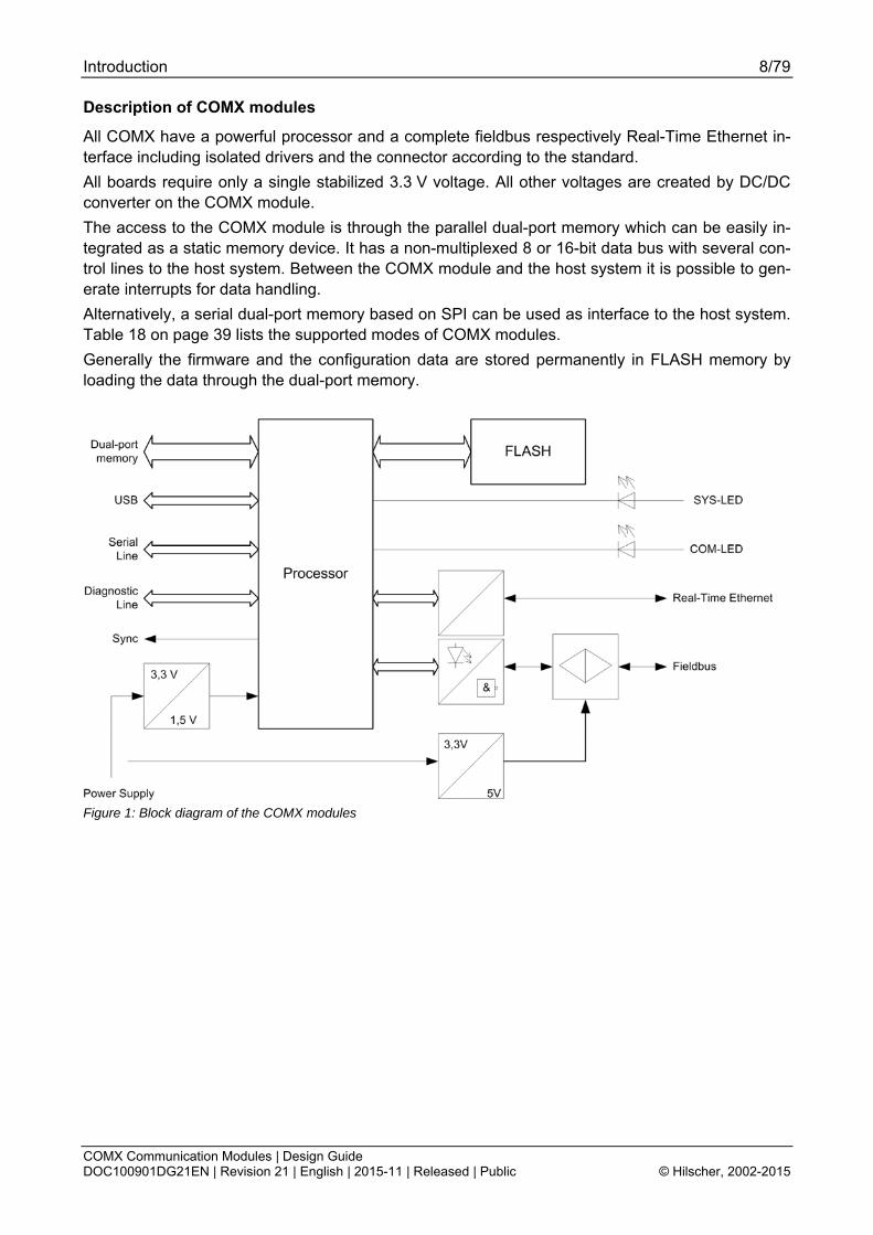
Description of COMX modules
All COMX have a powerful processor and a complete fieldbus respectively Real-Time Ethernet in-terface including isolated drivers and the connector according to the standard. All boards require only a single stabilized 3.3 V voltage. All other voltages are created by DC/DC converter on the COMX module. The access to the COMX module is through the parallel dual-port memory which can be easily in-tegrated as a static memory device. It has a non-multiplexed 8 or 16-bit data bus with several con-trol lines to the host system. Between the COMX module and the host system it is possible to gen-erate interrupts for data handling. Alternatively, a serial dual-port memory based on SPI can be used as interface to the host system. Table 18 on page 39 lists the supported modes of COMX modules. Generally the firmware and the configuration data are stored permanently in FLASH memory by loading the data through the dual-port memory.
Figure 1: Block diagram of the COMX modules
Introduction 9/79
COMX Communication Modules | Design Guide DOC100901DG21EN | Revision 21 | English | 2015-11 | Released | Public © Hilscher, 2002-2015
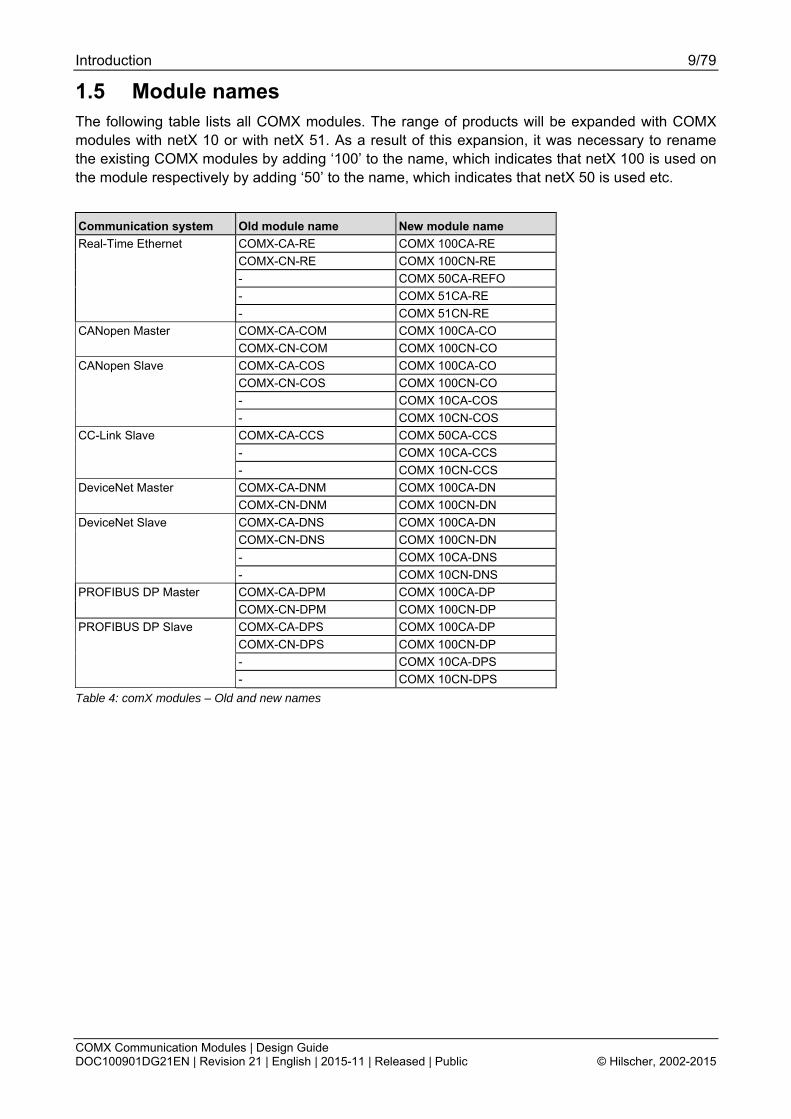
1.5 Module names The following table lists all COMX modules. The range of products will be expanded with COMX modules with netX 10 or with netX 51. As a result of this expansion, it was necessary to rename the existing COMX modules by adding 100 to the name, which indicates that netX 100 is used on the module respectively by adding 50 to the name, which indicates that netX 50 is used etc.
Communication system Old module name New module name COMX-CA-RE COMX 100CA-RE COMX-CN-RE COMX 100CN-RE - COMX 50CA-REFO - COMX 51CA-RE
Real-Time Ethernet
- COMX 51CN-RE COMX-CA-COM COMX 100CA-CO CANopen Master COMX-CN-COM COMX 100CN-CO COMX-CA-COS COMX 100CA-CO COMX-CN-COS COMX 100CN-CO - COMX 10CA-COS
CANopen Slave
- COMX 10CN-COS COMX-CA-CCS COMX 50CA-CCS - COMX 10CA-CCS
CC-Link Slave
- COMX 10CN-CCS COMX-CA-DNM COMX 100CA-DN DeviceNet Master COMX-CN-DNM COMX 100CN-DN COMX-CA-DNS COMX 100CA-DN COMX-CN-DNS COMX 100CN-DN - COMX 10CA-DNS
DeviceNet Slave
- COMX 10CN-DNS COMX-CA-DPM COMX 100CA-DP PROFIBUS DP Master COMX-CN-DPM COMX 100CN-DP COMX-CA-DPS COMX 100CA-DP COMX-CN-DPS COMX 100CN-DP - COMX 10CA-DPS
PROFIBUS DP Slave
- COMX 10CN-DPS Table 4: comX modules – Old and new names
Introduction 10/79
COMX Communication Modules | Design Guide DOC100901DG21EN | Revision 21 | English | 2015-11 | Released | Public © Hilscher, 2002-2015
1.6 References to documents This document refers to the following documents: [1] Hilscher Gesellschaft für Systemautomation mbH: Dual-Port Memory Interface Manual, netX
based products, Revision 12, English, 2012. [2] Hilscher Gesellschaft für Systemautomation mbH: User Manual, comX, Communication
Modules for Real-Time Ethernet and Fieldbus, Revision 5, English, 2015. [3] Hilscher Gesellschaft für Systemautomation mbH: Benutzerhandbuch, comX, Kommunica-
tionsmodule für Real-Time Ethernet und Feldbus, Revision 5, German, 2015. [4] Hilscher Gesellschaft für Systemautomation mbH: Getting Started Guide, Serial Dual-Port
Memory Interface with netX, Revision 1, English, 2012. [5] Hilscher Gesellschaft für Systemautomation mbH: Technical Data Reference Guide, netX 10,
Revision 0.9, English, 2011-12. [6] Hilscher Gesellschaft für Systemautomation mbH: Technical Data Reference Guide, netX
51/52, Revision 2, English, 2012-13. Table 5: References to documents
Introduction 11/79
COMX Communication Modules | Design Guide DOC100901DG21EN | Revision 21 | English | 2015-11 | Released | Public © Hilscher, 2002-2015
1.7 Legal notes 1.7.1 Copyright © Hilscher, 2002-2015, Hilscher Gesellschaft für Systemautomation mbH All rights reserved. The images, photographs and texts in the accompanying material (user manual, accompanying texts, documentation, etc.) are protected by German and international copyright law as well as in-ternational trade and protection provisions. You are not authorized to duplicate these in whole or in part using technical or mechanical methods (printing, photocopying or other methods), to manipu-late or transfer using electronic systems without prior written consent. You are not permitted to make changes to copyright notices, markings, trademarks or ownership declarations. The included diagrams do not take the patent situation into account. The company names and product descrip-tions included in this document may be trademarks or brands of the respective owners and may be trademarked or patented. Any form of further use requires the explicit consent of the respective rights owner.
1.7.2 Important notes The user manual, accompanying texts and the documentation were created for the use of the products by qualified experts, however, errors cannot be ruled out. For this reason, no guarantee can be made and neither juristic responsibility for erroneous information nor any liability can be as-sumed. Descriptions, accompanying texts and documentation included in the user manual do not present a guarantee nor any information about proper use as stipulated in the contract or a war-ranted feature. It cannot be ruled out that the user manual, the accompanying texts and the docu-mentation do not correspond exactly to the described features, standards or other data of the de-livered product. No warranty or guarantee regarding the correctness or accuracy of the information is assumed. We reserve the right to change our products and their specification as well as related user manu-als, accompanying texts and documentation at all times and without advance notice, without obli-gation to report the change. Changes will be included in future manuals and do not constitute any obligations. There is no entitlement to revisions of delivered documents. The manual delivered with the product applies. Hilscher Gesellschaft für Systemautomation mbH is not liable under any circumstances for direct, indirect, incidental or follow-on damage or loss of earnings resulting from the use of the information contained in this publication.

Introduction 12/79
COMX Communication Modules | Design Guide DOC100901DG21EN | Revision 21 | English | 2015-11 | Released | Public © Hilscher, 2002-2015
1.7.3 Exclusion of liability The software was produced and tested with utmost care by Hilscher Gesellschaft für Systemauto-mation mbH and is made available as is. No warranty can be assumed for the performance and flawlessness of the software for all usage conditions and cases and for the results produced when utilized by the user. Liability for any damages that may result from the use of the hardware or soft-ware or related documents, is limited to cases of intent or grossly negligent violation of significant contractual obligations. Indemnity claims for the violation of significant contractual obligations are limited to damages that are foreseeable and typical for this type of contract. It is strictly prohibited to use the software in the following areas: ! for military purposes or in weapon systems; ! for the design, construction, maintenance or operation of nuclear facilities; ! in air traffic control systems, air traffic or air traffic communication systems; ! in life support systems; ! in systems in which failures in the software could lead to personal injury or injuries leading to
death. We inform you that the software was not developed for use in dangerous environments requiring fail-proof control mechanisms. Use of the software in such an environment occurs at your own risk. No liability is assumed for damages or losses due to unauthorized use.
1.7.4 Warranty Although the hardware and software was developed with utmost care and tested intensively, Hil-scher Gesellschaft für Systemautomation mbH does not guarantee its suitability for any purpose not confirmed in writing. It cannot be guaranteed that the hardware and software will meet your re-quirements, that the use of the software operates without interruption and that the software is free of errors. No guarantee is made regarding infringements, violations of patents, rights of ownership or the freedom from interference by third parties. No additional guarantees or assurances are made regarding marketability, freedom of defect of title, integration or usability for certain purposes unless they are required in accordance with the law and cannot be limited. Warranty claims are limited to the right to claim rectification.
1.7.5 Export regulations The delivered product (including the technical data) is subject to export or import laws as well as the associated regulations of different counters, in particular those of Germany and the USA. The software may not be exported to countries where this is prohibited by the United States Export Administration Act and its additional provisions. You are obligated to comply with the regulations at your personal responsibility. We wish to inform you that you may require permission from state au-thorities to export, re-export or import the product.
Design-in - Mechanical aspects 13/79
COMX Communication Modules | Design Guide DOC100901DG21EN | Revision 21 | English | 2015-11 | Released | Public © Hilscher, 2002-2015
2 Design-in - Mechanical aspects 2.1 Type of COMX modules The following table gives an overview on the availability of the different COMX Modules.
Module Fieldbus / Protocol Type Connector
COMX 10 COMX 10CA-COS CANopen Slave angled COMX 10CN-COS CANopen Slave no COMX 10CA-CCS CC-Link Slave angled COMX 10CN-CCS CC-Link Slave no COMX 10CA-DPS PROFIBUS DP Slave angled COMX 10CN-DPS PROFIBUS DP Slave no COMX 10CA-DNS DeviceNet Slave angled COMX 10CN-DNS DeviceNet Slave no
COMX 50 COMX 50CA-CCS CC-Link Slave angled COMX 50CA-REFO PROFINET IO Device angled
COMX 51 COMX 51CA-RE Real-Time Ethernet Slave angled COMX 51CN-RE Real-Time Ethernet Slave no
COMX 100 COMX 100CA-CO CANopen Master or Slave
(depends on loaded firmware) angled
COMX 100CN-CO CANopen Master or Slave (depends on loaded firmware)
no
COMX 100CA-DN DeviceNet Master or Slave (depends on loaded firmware)
angled
COMX 100CN-DN DeviceNet Master or Slave (depends on loaded firmware)
no
COMX 100CA-DP PROFIBUS DP Master or Slave (depends on loaded firmware)
angled
COMX 100CN-DP PROFIBUS DP Master or Slave (depends on loaded firmware)
no
COMX 100CA-RE Real-Time Ethernet Master or Slave (depends on loaded firmware)
angled
COMX 100CN-RE Real-Time Ethernet Master or Slave (depends on loaded firmware)
no
Table 6: Available comX modules
Design-in - Mechanical aspects 14/79
COMX Communication Modules | Design Guide DOC100901DG21EN | Revision 21 | English | 2015-11 | Released | Public © Hilscher, 2002-2015
The following figures show the position of connector X1 and X2.
CA Types
Figure 2: COMX CA type - Connector X1
CN Types
Figure 3: COMX CN type - Connectors X1 and X2
Design-in - Mechanical aspects 15/79
COMX Communication Modules | Design Guide DOC100901DG21EN | Revision 21 | English | 2015-11 | Released | Public © Hilscher, 2002-2015
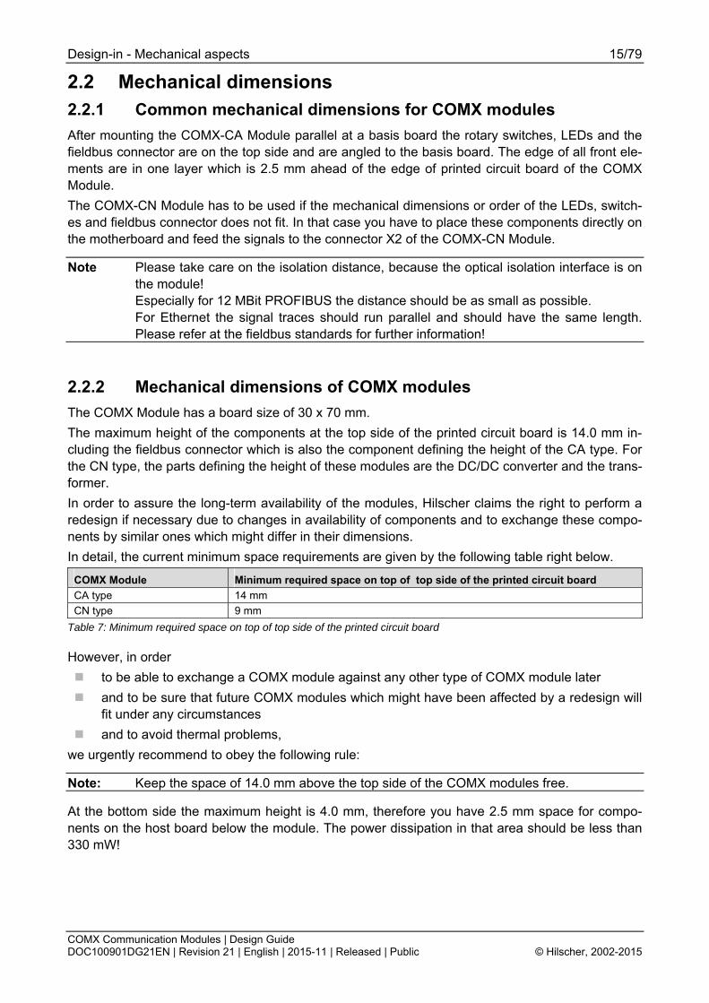
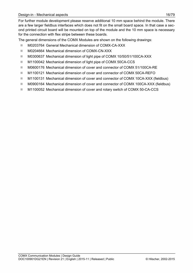
2.2 Mechanical dimensions 2.2.1 Common mechanical dimensions for COMX modules After mounting the COMX-CA Module parallel at a basis board the rotary switches, LEDs and the fieldbus connector are on the top side and are angled to the basis board. The edge of all front ele-ments are in one layer which is 2.5 mm ahead of the edge of printed circuit board of the COMX Module. The COMX-CN Module has to be used if the mechanical dimensions or order of the LEDs, switch-es and fieldbus connector does not fit. In that case you have to place these components directly on the motherboard and feed the signals to the connector X2 of the COMX-CN Module.
Note Please take care on the isolation distance, because the optical isolation interface is on the module! Especially for 12 MBit PROFIBUS the distance should be as small as possible. For Ethernet the signal traces should run parallel and should have the same length. Please refer at the fieldbus standards for further information!
2.2.2 Mechanical dimensions of COMX modules The COMX Module has a board size of 30 x 70 mm. The maximum height of the components at the top side of the printed circuit board is 14.0 mm in-cluding the fieldbus connector which is also the component defining the height of the CA type. For the CN type, the parts defining the height of these modules are the DC/DC converter and the trans-former. In order to assure the long-term availability of the modules, Hilscher claims the right to perform a redesign if necessary due to changes in availability of components and to exchange these compo-nents by similar ones which might differ in their dimensions. In detail, the current minimum space requirements are given by the following table right below.
COMX Module Minimum required space on top of top side of the printed circuit board CA type 14 mm CN type 9 mm
Table 7: Minimum required space on top of top side of the printed circuit board
However, in order ! to be able to exchange a COMX module against any other type of COMX module later ! and to be sure that future COMX modules which might have been affected by a redesign will
fit under any circumstances ! and to avoid thermal problems,
we urgently recommend to obey the following rule:
Note: Keep the space of 14.0 mm above the top side of the COMX modules free.
At the bottom side the maximum height is 4.0 mm, therefore you have 2.5 mm space for compo-nents on the host board below the module. The power dissipation in that area should be less than 330 mW!
Design-in - Mechanical aspects 16/79
COMX Communication Modules | Design Guide DOC100901DG21EN | Revision 21 | English | 2015-11 | Released | Public © Hilscher, 2002-2015
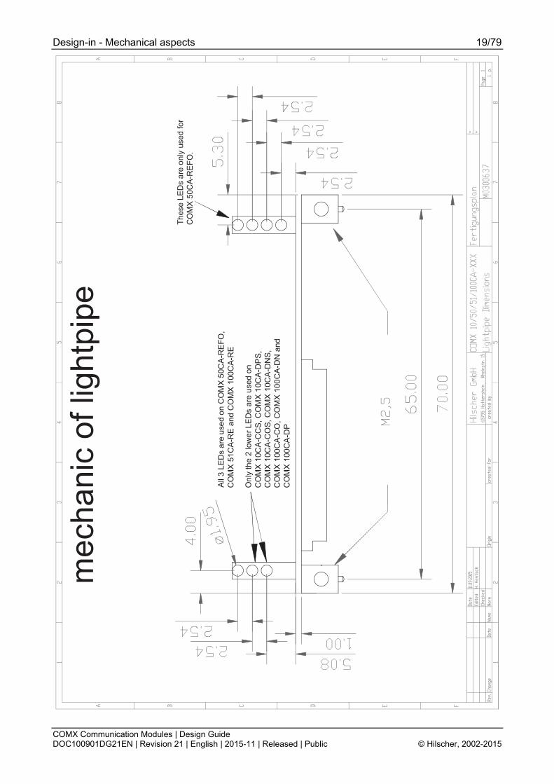
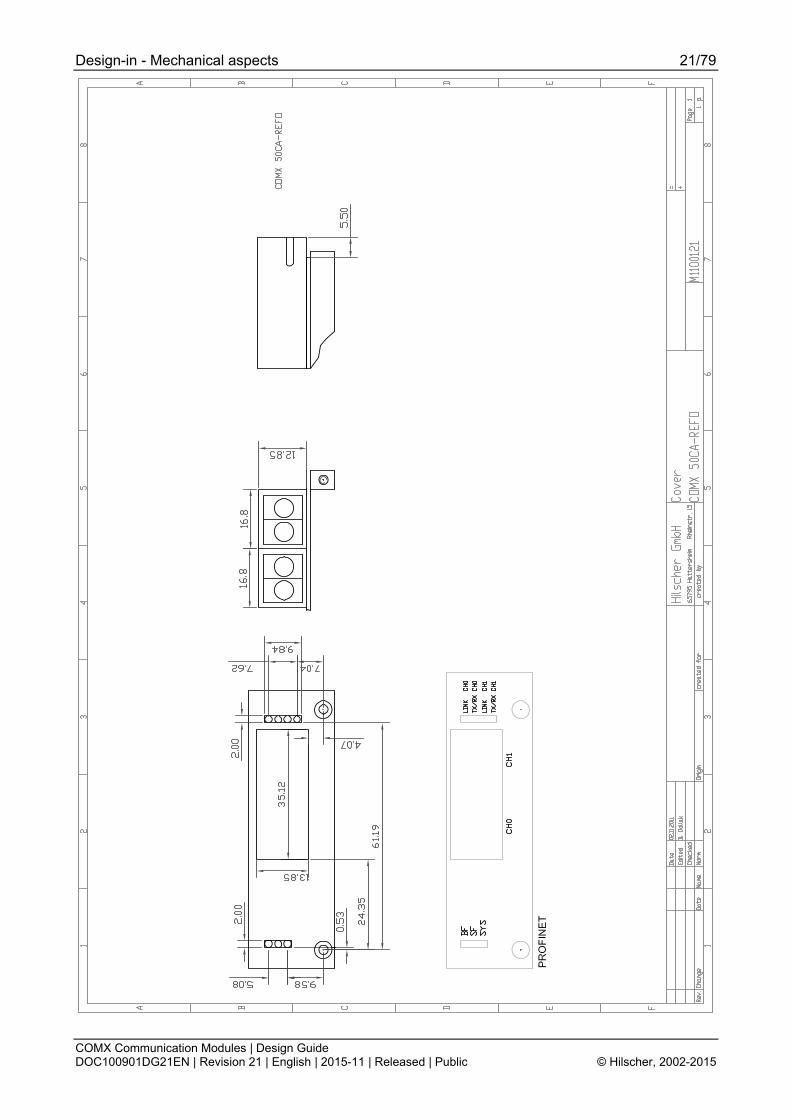
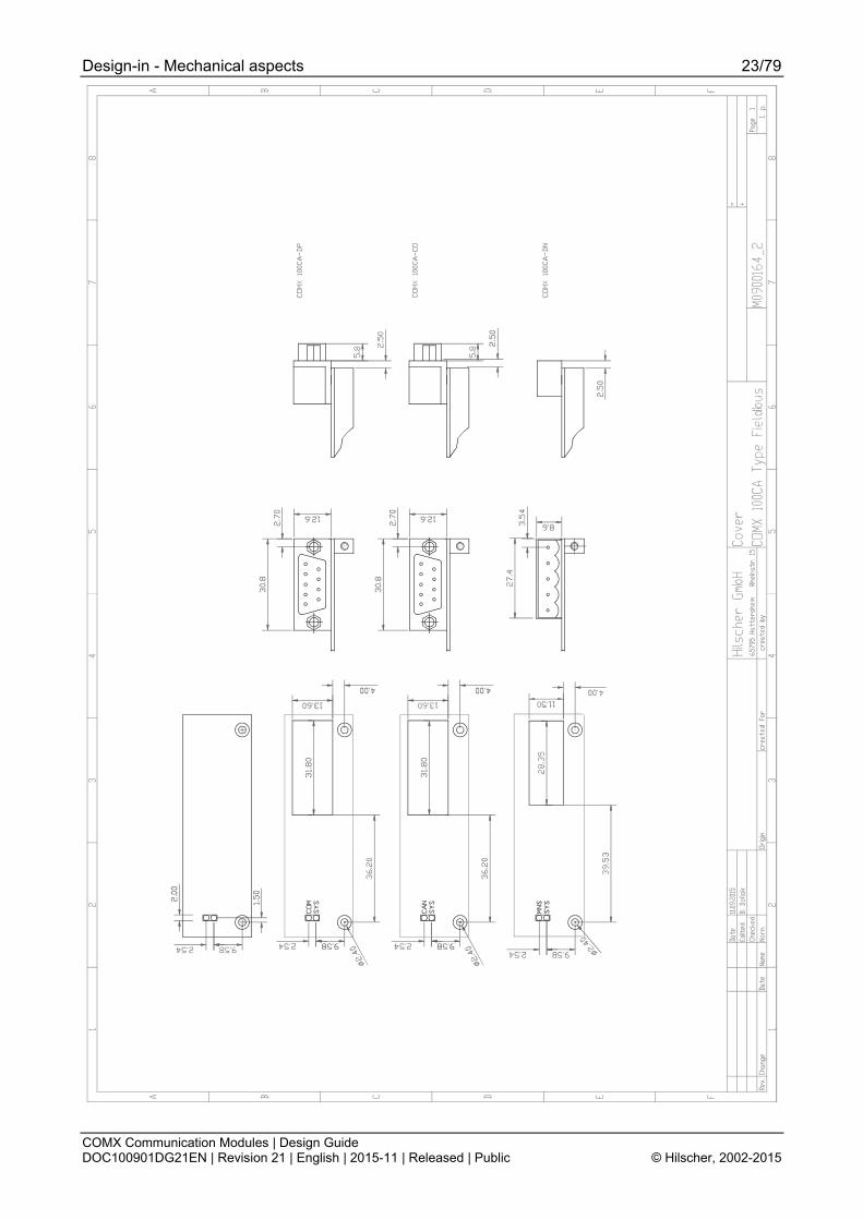
For further module development please reserve additional 10 mm space behind the module. There are a few larger fieldbus interfaces which does not fit on the small board space. In that case a sec-ond printed circuit board will be mounted on top of the module and the 10 mm space is necessary for the connection with flex stripe between these boards. The general dimensions of the COMX Modules are shown on the following drawings: ! M0203764 General Mechanical dimension of COMX-CA-XXX ! M0204664 Mechanical dimension of COMX-CN-XXX ! M0300637 Mechanical dimension of light pipe of COMX 10/50/51/100CA-XXX ! M1100042 Mechanical dimension of light pipe of COMX 50CA-CCS ! M0600176 Mechanical dimension of cover and connector of COMX 51/100CA-RE ! M1100121 Mechanical dimension of cover and connector of COMX 50CA-REFO ! M1100131 Mechanical dimension of cover and connector of COMX 10CA-XXX (fieldbus) ! M0900164 Mechanical dimension of cover and connector of COMX 100CA-XXX (fieldbus) ! M1100052 Mechanical dimension of cover and rotary switch of COMX 50-CA-CCS
Design-in - Mechanical aspects 17/79
COMX Communication Modules | Design Guide DOC100901DG21EN | Revision 21 | English | 2015-11 | Released | Public © Hilscher, 2002-2015
Design-in - Mechanical aspects 18/79
COMX Communication Modules | Design Guide DOC100901DG21EN | Revision 21 | English | 2015-11 | Released | Public © Hilscher, 2002-2015
Design-in - Mechanical aspects 19/79
COMX Communication Modules | Design Guide DOC100901DG21EN | Revision 21 | English | 2015-11 | Released | Public © Hilscher, 2002-2015
mec
hani
c of
ligh
tpip
e
All
3 LE
Ds
are
used
on
CO
MX
50C
A-R
EFO
,C
OM
X 5
1CA
-RE
and
CO
MX
100
CA-
RE
Onl
y th
e 2
low
er L
ED
s ar
e us
ed o
nC
OM
X 1
0CA
-CC
S, C
OM
X 1
0CA
-DP
S,
CO
MX
10C
A-C
OS
, CO
MX
10C
A-D
NS
,C
OM
X 1
00C
A-C
O, C
OM
X 10
0CA
-DN
and
CO
MX
100
CA
-DP
Thes
e LE
Ds
are
only
use
d fo
rC
OM
X 5
0CA
-RE
FO.
Design-in - Mechanical aspects 20/79
COMX Communication Modules | Design Guide DOC100901DG21EN | Revision 21 | English | 2015-11 | Released | Public © Hilscher, 2002-2015
PR
OFI
NE
T
Ethe
rNet
/IP
SER
CO
S S
lave
SER
CO
S M
aste
r
VA
RA
N
ETH
ER
NET
PO
WE
RLI
NK
Eth
erC
AT S
lave
Eth
erC
AT M
aste
r
CO
MX
100
CA
-RE
Seria
l num
ber 2
6000
and
hig
her
are
asse
mbl
ed w
ith A
mph
enol
RJS
SE
-538
1-02
Eth
erne
tco
nnec
tor
CO
MX
100
CA
-RE
Ser
ial n
umbe
r bel
ow 2
6000
wer
e as
sem
bled
with
Trx
com
TRJ1
9201
BGN
L Et
hern
etco
nnec
tors
Design-in - Mechanical aspects 21/79
COMX Communication Modules | Design Guide DOC100901DG21EN | Revision 21 | English | 2015-11 | Released | Public © Hilscher, 2002-2015

Design-in - Mechanical aspects 22/79
COMX Communication Modules | Design Guide DOC100901DG21EN | Revision 21 | English | 2015-11 | Released | Public © Hilscher, 2002-2015
Design-in - Mechanical aspects 23/79
COMX Communication Modules | Design Guide DOC100901DG21EN | Revision 21 | English | 2015-11 | Released | Public © Hilscher, 2002-2015

Design-in - Mechanical aspects 24/79
COMX Communication Modules | Design Guide DOC100901DG21EN | Revision 21 | English | 2015-11 | Released | Public © Hilscher, 2002-2015
Design-in - Mechanical aspects 25/79
COMX Communication Modules | Design Guide DOC100901DG21EN | Revision 21 | English | 2015-11 | Released | Public © Hilscher, 2002-2015
2.3 Type of connector The connector X1 for the host interface is a 50 pins SMT female type with a grid of 1.27 mm. The COMX modules of the CN series have an additional fieldbus connector X2 with 30 pins of the same family. The connector of the motherboard is the corresponding male type and can be ordered as follows: In Germany FJH die Steckverbinder GmbH Hinter dem Turm 7 D-55286 Wörrstadt Germany Tel. +49 (0) 67 32 / 93 27 -0 Fax +49 (0) 67 32 / 93 27 -27 Web: www.fjh.de Email: [email protected] 50 pin. Box header 127 KA - 050 SB 30 pin. Box header 127 KA - 030 SB World Wide SAMTEC www.samtec.com Cheaper version 50 pin. Connector TFM - 125 - 02 - S - D A TFC - 125 - 02 - F - D A 30 pin. Connector TFM - 115 - 02 - S - D A TFC - 115 - 02 - F - D A
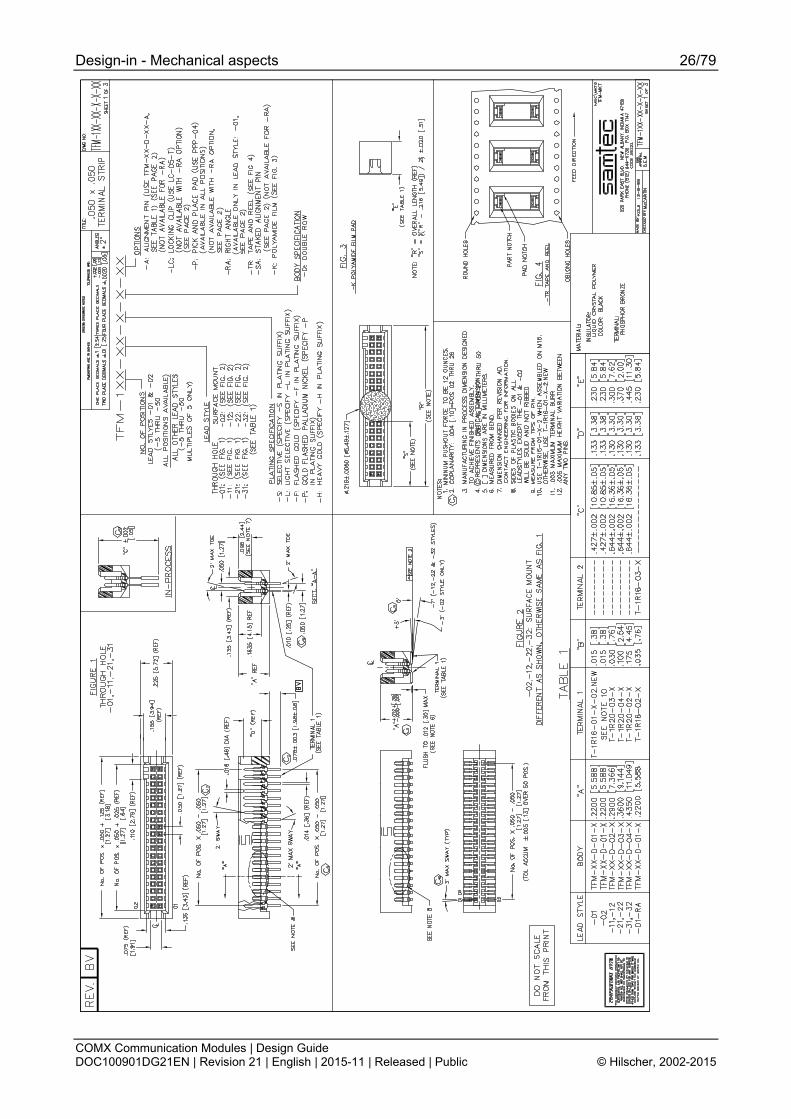
Note: Datasheet of SAMTEC TFM connector see next page. Please notice that the polarization of X1 and X2 is opposite to Pin 1!
The fieldbus connector on the module is defined by the fieldbus standard as followed:
Fieldbus Connector Vendor CANopen 9 pin, DSub, male div. Vendor DeviceNet 5 pin, COMBICON, male
Grid 5.08 mm i.e. PHOENIX Contact MSTBA2,5/5-5,08G-AU
Ethernet 8 pin, RJ45, female div. Vendor PROFIBUS 9 pin, DSub, female div. Vendor CC-Link 5 pin, COMBICON, male
Grid 5.08 mm i.e. PHOENIX Contact MSTBA2,5/5-G-AU
Table 8: Connector types
Please use the same type of connector on the motherboard if you have chosen the COMX CN type module.
Design-in - Mechanical aspects 26/79
COMX Communication Modules | Design Guide DOC100901DG21EN | Revision 21 | English | 2015-11 | Released | Public © Hilscher, 2002-2015
Design-in - Mechanical aspects 27/79
COMX Communication Modules | Design Guide DOC100901DG21EN | Revision 21 | English | 2015-11 | Released | Public © Hilscher, 2002-2015
2.3.1 Storage and contact reliability of host-side connector For the host-side connectors used in the comX communication modules (Samtec Types SFC-115-T2-L-D-A-K-TR and SFC-125-T2-L-D-A-K-TR), the following applies concerning storage stability and long-term immunity against contact failure: ! Hilscher only uses highly reliable connectors in the comX modules. The supplier of the con-
nector warrants a minimum expected storage time of 5 years without any loss of spring ten-sion when the connectors have been mounted. According to its general terms and condi-tions, Hilscher assures this warranted storage time to you.
! In order to preserve the spring tension and to improve the immunity against contact failure of the host-side connectors, the following storage conditions are recommended: ! Storage in dry package such as ESD bags which additionally can be heat-sealed. ! Alternatively: Controlled storage at a temperature of max. 25 °C and 50 % relative hu-
midity.
Design-in - Mechanical aspects 28/79
COMX Communication Modules | Design Guide DOC100901DG21EN | Revision 21 | English | 2015-11 | Released | Public © Hilscher, 2002-2015
2.4 Mounting of COMX modules The COMX Module has two metal blocks for mounting. This guarantees a robust mechanical con-struction and a solid connection to earth ground for the fieldbus connector. ! The metal block close to the fieldbus connector must be connected to PE (= Protective
Earth). ! The metal block close to the LEDs is not connected to the comX circuit and can be con-
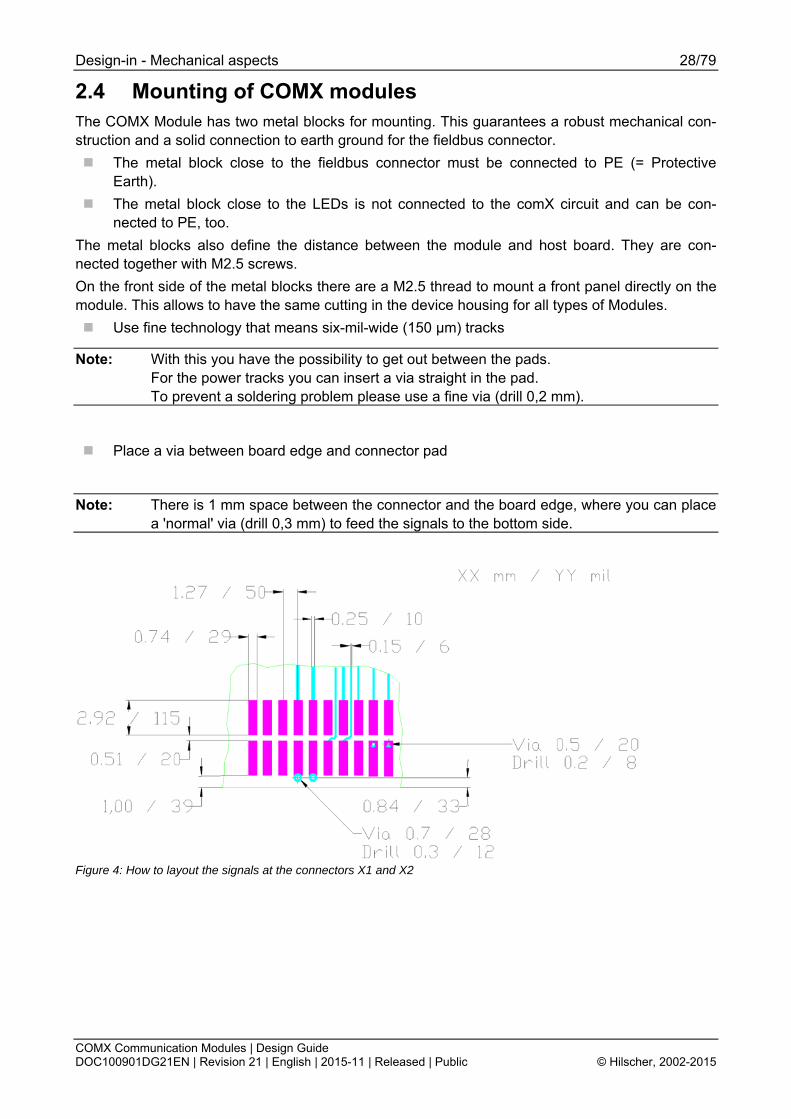
nected to PE, too. The metal blocks also define the distance between the module and host board. They are con-nected together with M2.5 screws. On the front side of the metal blocks there are a M2.5 thread to mount a front panel directly on the module. This allows to have the same cutting in the device housing for all types of Modules. ! Use fine technology that means six-mil-wide (150 μm) tracks
Note: With this you have the possibility to get out between the pads. For the power tracks you can insert a via straight in the pad. To prevent a soldering problem please use a fine via (drill 0,2 mm).
! Place a via between board edge and connector pad
Note: There is 1 mm space between the connector and the board edge, where you can place a 'normal' via (drill 0,3 mm) to feed the signals to the bottom side.
Figure 4: How to layout the signals at the connectors X1 and X2
Design-in - Mechanical aspects 29/79
COMX Communication Modules | Design Guide DOC100901DG21EN | Revision 21 | English | 2015-11 | Released | Public © Hilscher, 2002-2015
Three types of metal bolts are used. The following table lists the usage for each COMX Module.
COM Type Left Side Right Side COS, DNS, DPS COM-CA-B20X5 COM-CA-B24X5 COMX 10CA CCS COM-CA-B20X5 COM-CA-B20X5
COMX 10CN CCS, COS, DNS, DPS COM-CA-B20X5 COM-CA-B20X5 COMX 50CA CCS, REFO COM-CA-B20X5 COM-CA-B20X5 COMX 51CA RE COM-CA-B20X5 COM-CA-B31,5X5 COMX 51CN RE COM-CA-B20X5 COM-CA-B20X5
CO, DN, DP, CC COM-CA-B20X5 COM-CA-B24X5 COMX 100CA RE COM-CA-B20X5 COM-CA-B31,5X5
COMX 100CN COM, COS, DNM, DNS, DPM, DPS, RE COM-CA-B20X5 COM-CA-B20X5 Table 9: Usage of bolt for COMX modules
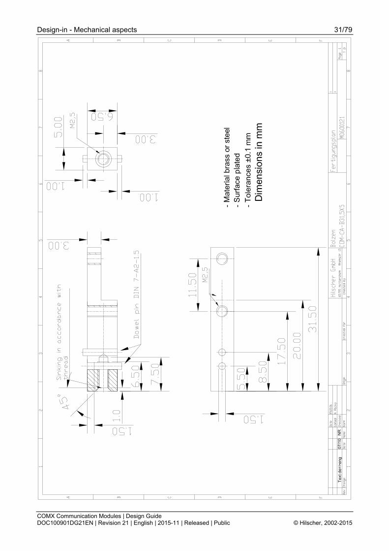
The drawings for the bolts are shown on the following drawings: ! M0100084 Mechanical dimension of Bolt COM-CA-B20X5 ! M0600121 Mechanical dimension of Bolt COM-CA-B31,5X5 ! M0900102 Mechanical dimension of Bolt COM-CA-B24X5
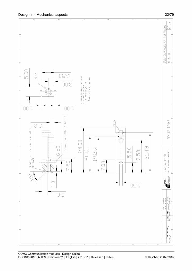
The drawing for an assembled bolt is shown on the following drawing: ! M0200402 Mechanical dimension how to assemble COM-CA-XXX on the mother board

Design-in - Mechanical aspects 30/79
COMX Communication Modules | Design Guide DOC100901DG21EN | Revision 21 | English | 2015-11 | Released | Public © Hilscher, 2002-2015
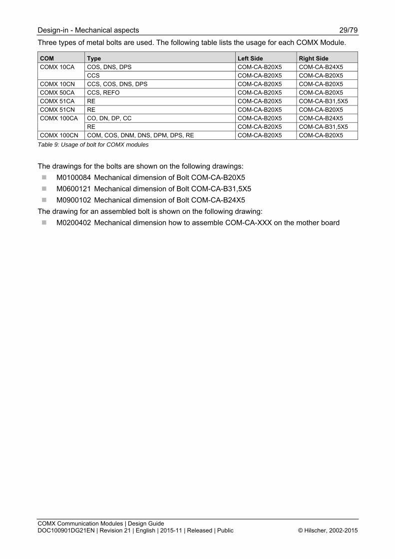
Design-in - Mechanical aspects 31/79
COMX Communication Modules | Design Guide DOC100901DG21EN | Revision 21 | English | 2015-11 | Released | Public © Hilscher, 2002-2015
Design-in - Mechanical aspects 32/79
COMX Communication Modules | Design Guide DOC100901DG21EN | Revision 21 | English | 2015-11 | Released | Public © Hilscher, 2002-2015
Design-in - Mechanical aspects 33/79
COMX Communication Modules | Design Guide DOC100901DG21EN | Revision 21 | English | 2015-11 | Released | Public © Hilscher, 2002-2015
Design-in - Mechanical aspects 34/79
COMX Communication Modules | Design Guide DOC100901DG21EN | Revision 21 | English | 2015-11 | Released | Public © Hilscher, 2002-2015
2.5 Material recommendation for the faceplate For achieving good emission and immunity behavior of your device under construction into which the COMX Module is integrated, we urgently recommend to use metal as material for the covering faceplate. Do not use plastics!
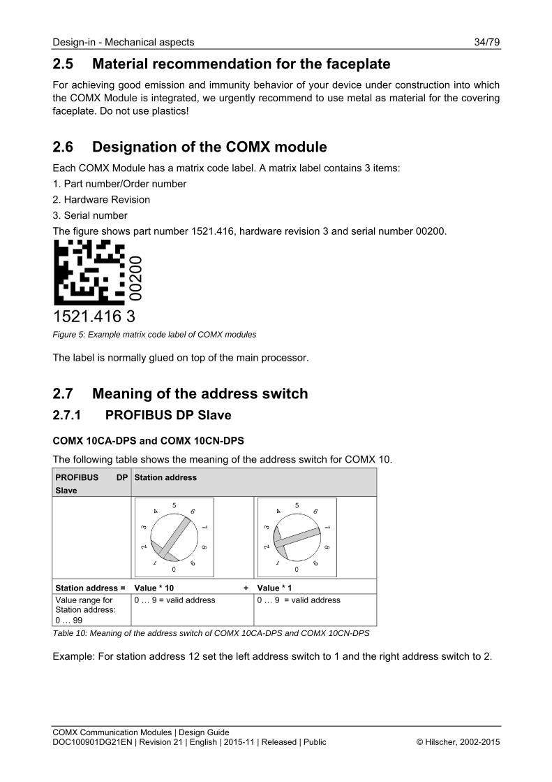
2.6 Designation of the COMX module Each COMX Module has a matrix code label. A matrix label contains 3 items: 1. Part number/Order number 2. Hardware Revision 3. Serial number The figure shows part number 1521.416, hardware revision 3 and serial number 00200.
Figure 5: Example matrix code label of COMX modules
The label is normally glued on top of the main processor.
2.7 Meaning of the address switch 2.7.1 PROFIBUS DP Slave
COMX 10CA-DPS and COMX 10CN-DPS
The following table shows the meaning of the address switch for COMX 10.
PROFIBUS DP Slave
Station address
Station address = Value * 10 + Value * 1 Value range for Station address: 0 99
0 9 = valid address 0 9 = valid address
Table 10: Meaning of the address switch of COMX 10CA-DPS and COMX 10CN-DPS
Example: For station address 12 set the left address switch to 1 and the right address switch to 2.
Design-in - Mechanical aspects 35/79
COMX Communication Modules | Design Guide DOC100901DG21EN | Revision 21 | English | 2015-11 | Released | Public © Hilscher, 2002-2015
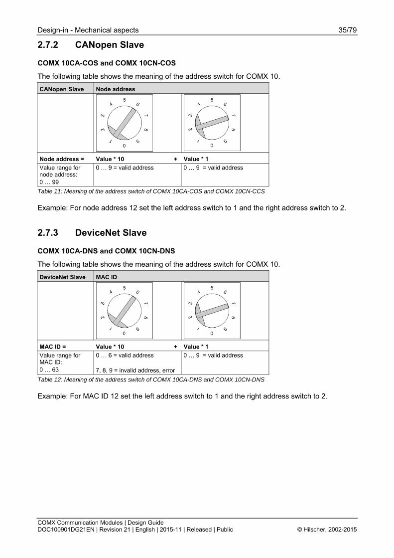
2.7.2 CANopen Slave
COMX 10CA-COS and COMX 10CN-COS
The following table shows the meaning of the address switch for COMX 10.
CANopen Slave Node address
Node address = Value * 10 + Value * 1 Value range for node address: 0 99
0 9 = valid address 0 9 = valid address
Table 11: Meaning of the address switch of COMX 10CA-COS and COMX 10CN-CCS
Example: For node address 12 set the left address switch to 1 and the right address switch to 2.
2.7.3 DeviceNet Slave
COMX 10CA-DNS and COMX 10CN-DNS
The following table shows the meaning of the address switch for COMX 10.
DeviceNet Slave MAC ID
MAC ID = Value * 10 + Value * 1 Value range for MAC ID: 0 63
0 6 = valid address 7, 8, 9 = invalid address, error
0 9 = valid address
Table 12: Meaning of the address switch of COMX 10CA-DNS and COMX 10CN-DNS
Example: For MAC ID 12 set the left address switch to 1 and the right address switch to 2.

Design-in - Mechanical aspects 36/79
COMX Communication Modules | Design Guide DOC100901DG21EN | Revision 21 | English | 2015-11 | Released | Public © Hilscher, 2002-2015
2.7.4 CC-Link Slave 2.7.4.1 COMX 10CA-CCS and COMX 10CN-CCS The following table shows the meaning of the address and baudrate switches for COMX 10.
CC-Link Slave Station address Baudrate
Station address = Value * 10 + Value * 1
Value range for Station address: 1 64
0 6 = valid address 7, 8, 9 = invalid address, error
0, 1, , 8, 9 = valid address 0 = 156 kBaud 1 = 625 kBaud 2 = 2,5 MBaud 3 = 5 MBaud 4 = 10 MBaud 5 ... 9 = Invalid, error
Table 13: Meaning of the address and baudrate switch of COMX 10CA-CCS and COMX 10CN-CCS
Example: For station address 12 set the left switch to 1 and the middle switch to 2. For baudrate 156 kBaud set the right switch to 0. Depending on the configuration parameter Number of stations, the value range for station address is:
Number of stations Value range for station address 1 1 64 2 1 63 3 1 62 4 1 61
Table 14: Value range for station address depending on number of stations

Design-in - Mechanical aspects 37/79
COMX Communication Modules | Design Guide DOC100901DG21EN | Revision 21 | English | 2015-11 | Released | Public © Hilscher, 2002-2015
2.7.4.2 COMX 50CA-CCS The following table shows the meaning of the address and baudrate switch for COMX 50.
CC-Link Slave Station address Baudrate
Station address = Value * 16 + Value * 1
Value range for Station address: 1 64
0 4 = valid address 5, 6, 7, 8, 9, A F = invalid address, error
0, 1, , 8, 9, A, , F = valid address
0 = 156 kBaud 1 = 625 kBaud 2 = 2,5 MBaud 3 = 5 MBaud 4 = 10 MBaud 5 ... F = Invalid, error
Table 15: Meaning of the address and baudrate switch of COMX 50CA-CCS
Example: For CC-Link station address 18 set the left switch to 1 and the middle switch to 2. For baudrate 156 kBaud set the right switch to 0. Depending on the configuration parameter Number of stations, the value range for station address is:
Number of stations Value range for station address 1 1 64 2 1 63 3 1 62 4 1 61
Table 16: Value range for station address depending on number of stations
Design-in - Mechanical aspects 38/79
COMX Communication Modules | Design Guide DOC100901DG21EN | Revision 21 | English | 2015-11 | Released | Public © Hilscher, 2002-2015
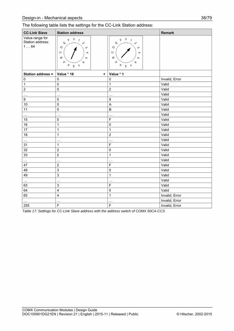
The following table lists the settings for the CC-Link Station address:
CC-Link Slave Station address Remark Value range for Station address: 1 64
Station address = Value * 16 + Value * 1
0 0 0 Invalid, Error 1 0 1 Valid 2 0 2 Valid Valid 9 0 9 Valid 10 0 A Valid 11 0 B Valid Valid 15 0 F Valid 16 1 0 Valid 17 1 1 Valid 18 1 2 Valid Valid 31 1 F Valid 32 2 0 Valid 33 2 1 Valid Valid 47 2 F Valid 48 3 0 Valid 49 3 1 Valid Valid 63 3 F Valid 64 4 0 Valid 65 4 1 Invalid, Error Invalid, Error 255 F F Invalid, Error
Table 17: Settings for CC-Link Slave address with the address switch of COMX 50CA-CCS
Design-in - Electrical aspects 39/79
COMX Communication Modules | Design Guide DOC100901DG21EN | Revision 21 | English | 2015-11 | Released | Public © Hilscher, 2002-2015
3 Design-in - Electrical aspects 3.1 Host interface Attention! All COMX modules have an operation voltage of 3.3 V which reduces the power con-
sumption. Therefore the voltage levels of the signals have to be not higher than 3.3 V otherwise the module will be damaged.
The next sections show an overview of the signal pin assignment of the system connector.
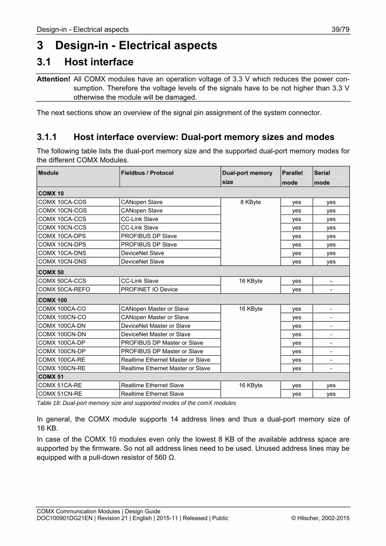
3.1.1 Host interface overview: Dual-port memory sizes and modes The following table lists the dual-port memory size and the supported dual-port memory modes for the different COMX Modules.
Module Fieldbus / Protocol Dual-port memory size
Parallel mode
Serial mode
COMX 10 COMX 10CA-COS CANopen Slave 8 KByte yes yes COMX 10CN-COS CANopen Slave yes yes COMX 10CA-CCS CC-Link Slave yes yes COMX 10CN-CCS CC-Link Slave yes yes COMX 10CA-DPS PROFIBUS DP Slave yes yes COMX 10CN-DPS PROFIBUS DP Slave yes yes COMX 10CA-DNS DeviceNet Slave yes yes COMX 10CN-DNS DeviceNet Slave yes yes
COMX 50 COMX 50CA-CCS CC-Link Slave 16 KByte yes - COMX 50CA-REFO PROFINET IO Device yes -
COMX 100 COMX 100CA-CO CANopen Master or Slave 16 KByte yes - COMX 100CN-CO CANopen Master or Slave yes - COMX 100CA-DN DeviceNet Master or Slave yes - COMX 100CN-DN DeviceNet Master or Slave yes - COMX 100CA-DP PROFIBUS DP Master or Slave yes - COMX 100CN-DP PROFIBUS DP Master or Slave yes - COMX 100CA-RE Realtime Ethernet Master or Slave yes - COMX 100CN-RE Realtime Ethernet Master or Slave yes - COMX 51 COMX 51CA-RE Realtime Ethernet Slave 16 KByte yes yes COMX 51CN-RE Realtime Ethernet Slave yes yes Table 18: Dual-port memory size and supported modes of the comX modules
In general, the COMX module supports 14 address lines and thus a dual-port memory size of 16 KB. In case of the COMX 10 modules even only the lowest 8 KB of the available address space are supported by the firmware. So not all address lines need to be used. Unused address lines may be equipped with a pull-down resistor of 560 Ω.
Design-in - Electrical aspects 40/79
COMX Communication Modules | Design Guide DOC100901DG21EN | Revision 21 | English | 2015-11 | Released | Public © Hilscher, 2002-2015
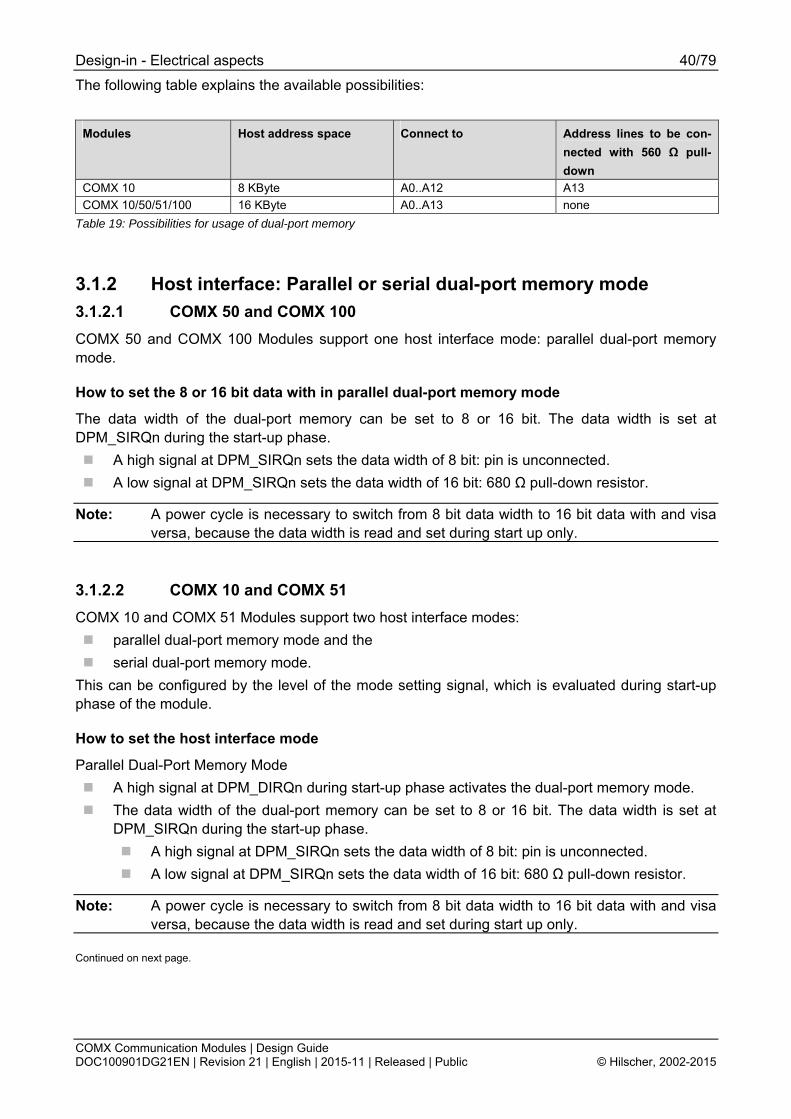
The following table explains the available possibilities:
Modules Host address space Connect to Address lines to be con-nected with 560 Ω pull-down
COMX 10 8 KByte A0..A12 A13 COMX 10/50/51/100 16 KByte A0..A13 none
Table 19: Possibilities for usage of dual-port memory
3.1.2 Host interface: Parallel or serial dual-port memory mode 3.1.2.1 COMX 50 and COMX 100 COMX 50 and COMX 100 Modules support one host interface mode: parallel dual-port memory mode.
How to set the 8 or 16 bit data with in parallel dual-port memory mode
The data width of the dual-port memory can be set to 8 or 16 bit. The data width is set at DPM_SIRQn during the start-up phase. ! A high signal at DPM_SIRQn sets the data width of 8 bit: pin is unconnected. ! A low signal at DPM_SIRQn sets the data width of 16 bit: 680 Ω pull-down resistor.
Note: A power cycle is necessary to switch from 8 bit data width to 16 bit data with and visa versa, because the data width is read and set during start up only.
3.1.2.2 COMX 10 and COMX 51 COMX 10 and COMX 51 Modules support two host interface modes: ! parallel dual-port memory mode and the ! serial dual-port memory mode.
This can be configured by the level of the mode setting signal, which is evaluated during start-up phase of the module.
How to set the host interface mode
Parallel Dual-Port Memory Mode ! A high signal at DPM_DIRQn during start-up phase activates the dual-port memory mode. ! The data width of the dual-port memory can be set to 8 or 16 bit. The data width is set at
DPM_SIRQn during the start-up phase. ! A high signal at DPM_SIRQn sets the data width of 8 bit: pin is unconnected. ! A low signal at DPM_SIRQn sets the data width of 16 bit: 680 Ω pull-down resistor.
Note: A power cycle is necessary to switch from 8 bit data width to 16 bit data with and visa versa, because the data width is read and set during start up only.
Continued on next page.
Design-in - Electrical aspects 41/79
COMX Communication Modules | Design Guide DOC100901DG21EN | Revision 21 | English | 2015-11 | Released | Public © Hilscher, 2002-2015
Serial Dual-Port Memory Mode ! A low signal at DPM_DIRQn activates the serial dual-port memory mode (via a 680 Ω pull-
down resistor). Pin DPM_SIRQn: let the input open. Signals DPM_DIRQn and DPM_SIRQn have a pull-up resistor of 4,7 kΩ on the COMX 10 or 51 Module.
Important: Never drive the host interface mode signal (DPM_DIRQn). Instead, operation with pull-down and pull-up resistors is recommended.
Design-in - Electrical aspects 42/79
COMX Communication Modules | Design Guide DOC100901DG21EN | Revision 21 | English | 2015-11 | Released | Public © Hilscher, 2002-2015
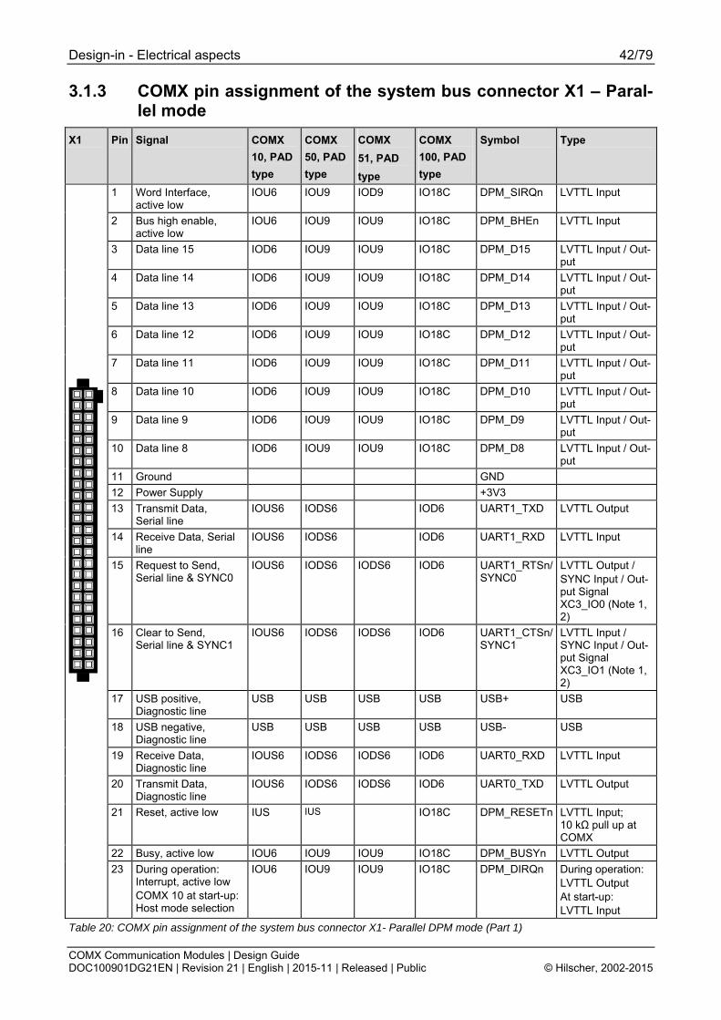
3.1.3 COMX pin assignment of the system bus connector X1 Paral-lel mode
X1 Pin Signal COMX 10, PAD type
COMX 50, PAD type
COMX 51, PAD type
COMX 100, PAD type
Symbol Type
1 Word Interface, active low
IOU6 IOU9 IOD9 IO18C DPM_SIRQn LVTTL Input
2 Bus high enable, active low
IOU6 IOU9 IOU9 IO18C DPM_BHEn LVTTL Input
3 Data line 15 IOD6 IOU9 IOU9 IO18C DPM_D15 LVTTL Input / Out-put
4 Data line 14 IOD6 IOU9 IOU9 IO18C DPM_D14 LVTTL Input / Out-put
5 Data line 13 IOD6 IOU9 IOU9 IO18C DPM_D13 LVTTL Input / Out-put
6 Data line 12 IOD6 IOU9 IOU9 IO18C DPM_D12 LVTTL Input / Out-put
7 Data line 11 IOD6 IOU9 IOU9 IO18C DPM_D11 LVTTL Input / Out-put
8 Data line 10 IOD6 IOU9 IOU9 IO18C DPM_D10 LVTTL Input / Out-put
9 Data line 9 IOD6 IOU9 IOU9 IO18C DPM_D9 LVTTL Input / Out-put
10 Data line 8 IOD6 IOU9 IOU9 IO18C DPM_D8 LVTTL Input / Out-put
11 Ground GND 12 Power Supply +3V3 13 Transmit Data,
Serial line IOUS6 IODS6 IOD6 UART1_TXD LVTTL Output
14 Receive Data, Serial line
IOUS6 IODS6 IOD6 UART1_RXD LVTTL Input
15 Request to Send, Serial line & SYNC0
IOUS6 IODS6 IODS6 IOD6 UART1_RTSn/ SYNC0
LVTTL Output / SYNC Input / Out-put Signal XC3_IO0 (Note 1, 2)
16 Clear to Send, Serial line & SYNC1
IOUS6 IODS6 IODS6 IOD6 UART1_CTSn/ SYNC1
LVTTL Input / SYNC Input / Out-put Signal XC3_IO1 (Note 1, 2)
17 USB positive, Diagnostic line
USB USB USB USB USB+ USB
18 USB negative, Diagnostic line
USB USB USB USB USB- USB
19 Receive Data, Diagnostic line
IOUS6 IODS6 IODS6 IOD6 UART0_RXD LVTTL Input
20 Transmit Data, Diagnostic line
IOUS6 IODS6 IODS6 IOD6 UART0_TXD LVTTL Output
21 Reset, active low IUS IUS IO18C DPM_RESETn LVTTL Input; 10 kΩ pull up at COMX
22 Busy, active low IOU6 IOU9 IOU9 IO18C DPM_BUSYn LVTTL Output
23 During operation: Interrupt, active low COMX 10 at start-up: Host mode selection
IOU6 IOU9 IOU9 IO18C DPM_DIRQn During operation: LVTTL Output At start-up: LVTTL Input
Table 20: COMX pin assignment of the system bus connector X1- Parallel DPM mode (Part 1)
Design-in - Electrical aspects 43/79
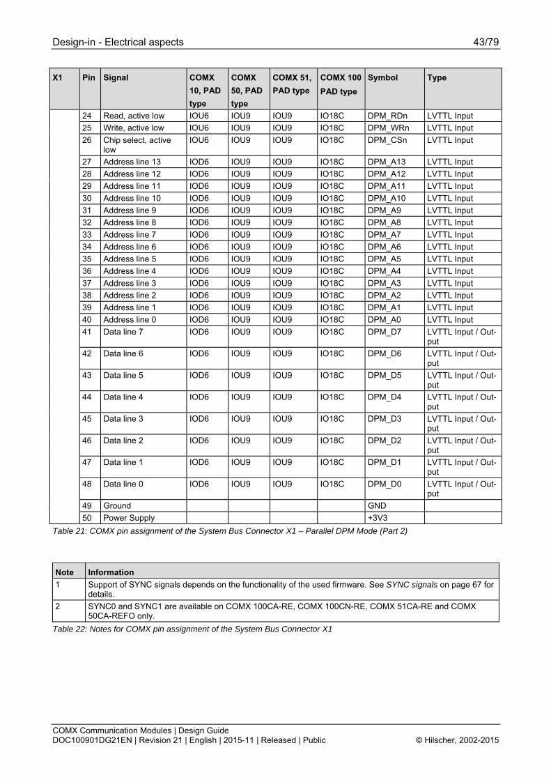
COMX Communication Modules | Design Guide DOC100901DG21EN | Revision 21 | English | 2015-11 | Released | Public © Hilscher, 2002-2015
X1 Pin Signal COMX 10, PAD type
COMX 50, PAD type
COMX 51, PAD type
COMX 100PAD type
Symbol Type
24 Read, active low IOU6 IOU9 IOU9 IO18C DPM_RDn LVTTL Input 25 Write, active low IOU6 IOU9 IOU9 IO18C DPM_WRn LVTTL Input 26 Chip select, active
low IOU6 IOU9 IOU9 IO18C DPM_CSn LVTTL Input
27 Address line 13 IOD6 IOU9 IOU9 IO18C DPM_A13 LVTTL Input 28 Address line 12 IOD6 IOU9 IOU9 IO18C DPM_A12 LVTTL Input 29 Address line 11 IOD6 IOU9 IOU9 IO18C DPM_A11 LVTTL Input 30 Address line 10 IOD6 IOU9 IOU9 IO18C DPM_A10 LVTTL Input 31 Address line 9 IOD6 IOU9 IOU9 IO18C DPM_A9 LVTTL Input 32 Address line 8 IOD6 IOU9 IOU9 IO18C DPM_A8 LVTTL Input 33 Address line 7 IOD6 IOU9 IOU9 IO18C DPM_A7 LVTTL Input 34 Address line 6 IOD6 IOU9 IOU9 IO18C DPM_A6 LVTTL Input 35 Address line 5 IOD6 IOU9 IOU9 IO18C DPM_A5 LVTTL Input 36 Address line 4 IOD6 IOU9 IOU9 IO18C DPM_A4 LVTTL Input 37 Address line 3 IOD6 IOU9 IOU9 IO18C DPM_A3 LVTTL Input 38 Address line 2 IOD6 IOU9 IOU9 IO18C DPM_A2 LVTTL Input 39 Address line 1 IOD6 IOU9 IOU9 IO18C DPM_A1 LVTTL Input 40 Address line 0 IOD6 IOU9 IOU9 IO18C DPM_A0 LVTTL Input 41 Data line 7 IOD6 IOU9 IOU9 IO18C DPM_D7 LVTTL Input / Out-
put 42 Data line 6 IOD6 IOU9 IOU9 IO18C DPM_D6 LVTTL Input / Out-
put 43 Data line 5 IOD6 IOU9 IOU9 IO18C DPM_D5 LVTTL Input / Out-
put 44 Data line 4 IOD6 IOU9 IOU9 IO18C DPM_D4 LVTTL Input / Out-
put 45 Data line 3 IOD6 IOU9 IOU9 IO18C DPM_D3 LVTTL Input / Out-
put 46 Data line 2 IOD6 IOU9 IOU9 IO18C DPM_D2 LVTTL Input / Out-
put 47 Data line 1 IOD6 IOU9 IOU9 IO18C DPM_D1 LVTTL Input / Out-
put 48 Data line 0 IOD6 IOU9 IOU9 IO18C DPM_D0 LVTTL Input / Out-
put 49 Ground GND
50 Power Supply +3V3 Table 21: COMX pin assignment of the System Bus Connector X1 – Parallel DPM Mode (Part 2)
Note Information 1 Support of SYNC signals depends on the functionality of the used firmware. See SYNC signals on page 67 for
details. 2 SYNC0 and SYNC1 are available on COMX 100CA-RE, COMX 100CN-RE, COMX 51CA-RE and COMX
50CA-REFO only. Table 22: Notes for COMX pin assignment of the System Bus Connector X1
Design-in - Electrical aspects 44/79
COMX Communication Modules | Design Guide DOC100901DG21EN | Revision 21 | English | 2015-11 | Released | Public © Hilscher, 2002-2015
3.1.4 COMX pin assignment of the system bus connector X1 Serial mode
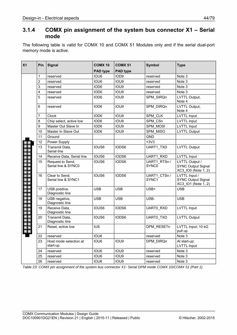
The following table is valid for COMX 10 and COMX 51 Modules only and if the serial dual-port memory mode is active.
X1 Pin Signal COMX 10 PAD type
COMX 51 PAD type
Symbol Type
1 reserved IOU6 IOD9 reserved Note 3 2 reserved IOU6 IOU9 reserved Note 3 3 reserved IOD6 IOU9 reserved Note 3 4 reserved IOD6 IOU9 reserved Note 3 5 reserved IOD6 IOU9 SPM_SIRQn LVTTL Output,
Note 4 6 reserved IOD6 IOU9 SPM_DIRQn LVTTL Output,
Note 4 7 Clock IOD6 IOU9 SPM_CLK LVTTL Input 8 Chip select, active low IOD6 IOU9 SPM_CSn LVTTL Input 9 Master Out Slave In IOD6 IOU9 SPM_MOSI LVTTL Input 10 Master In Slave Out IOD6 IOU9 SPM_MISO LVTTL Output 11 Ground GND 12 Power Supply +3V3 13 Transmit Data,
Serial line IOUS6 IODS6 UART1_TXD LVTTL Output
14 Receive Data, Serial line IOUS6 IODS6 UART1_RXD LVTTL Input 15 Request to Send,
Serial line & SYNC0 IOUS6 IODS6 UART1_RTSn /
SYNC0 LVTTL Output / SYNC Output Signal XC3_IO0 (Note 1, 2)
16 Clear to Send, Serial line & SYNC1
IOUS6 IODS6 UART1_CTSn / SYNC1
LVTTL Input / SYNC Output Signal XC3_IO1 (Note 1, 2)
17 USB positive, Diagnostic line
USB USB USB+ USB
18 USB negative, Diagnostic line
USB USB USB- USB
19 Receive Data, Diagnostic line
IOUS6 IODS6 UART0_RXD LVTTL Input
20 Transmit Data, Diagnostic line
IOUS6 IODS6 UART0_TXD LVTTL Output
21 Reset, active low IUS DPM_RESETn LVTTL Input; 10 kΩ pull up
22 reserved IOU6 reserved Note 3 23 Host mode selection at
start-up IOU6 IOU9 DPM_DIRQn At start-up:
LVTTL Input 24 reserved IOU6 IOU9 reserved Note 3 25 reserved IOU6 IOU9 reserved Note 3
26 reserved IOU6 IOU9 reserved Note 3 Table 23: COMX pin assignment of the system bus connector X1- Serial DPM mode COMX 10/COMX 51 (Part 1)
Design-in - Electrical aspects 45/79
COMX Communication Modules | Design Guide DOC100901DG21EN | Revision 21 | English | 2015-11 | Released | Public © Hilscher, 2002-2015
X1 Pin Signal COMX 10 PAD type
COMX 51 PAD type
Symbol Type
27 reserved IOD6 IOU9 reserved Note 3 28 reserved IOD6 IOU9 reserved Note 3 29 reserved IOD6 IOU9 reserved Note 3 30 reserved IOD6 IOU9 reserved Note 3 31 reserved IOD6 IOU9 reserved Note 3 32 reserved IOD6 IOU9 reserved Note 3 33 reserved IOD6 IOU9 reserved Note 3 34 reserved IOD6 IOU9 reserved Note 3 35 reserved IOD6 IOU9 reserved Note 3 36 reserved IOD6 IOU9 reserved Note 3 37 reserved IOD6 IOU9 reserved Note 3 38 reserved IOD6 IOU9 reserved Note 3 39 reserved IOD6 IOU9 reserved Note 3 40 reserved IOD6 IOU9 reserved Note 3 41 reserved IOD6 IOU9 reserved Note 3 42 reserved IOD6 IOU9 reserved Note 3 43 reserved IOD6 IOU9 reserved Note 3 44 reserved IOD6 IOU9 reserved Note 3 45 reserved IOD6 IOU9 reserved Note 3 46 reserved IOD6 IOU9 reserved Note 3 47 reserved IOD6 IOU9 reserved Note 3 48 reserved IOD6 IOU9 reserved Note 3 49 Ground GND
50 Power Supply +3V3 Table 24: COMX pin assignment of the System Bus Connector X1 – Serial DPM Mode COMX 10/COMX 51 (Part 2)
Note Information 1 Support of SYNC signals depends on the functionality of the used firmware. See SYNC signals on page 67 for
details. 2 SYNC0 and SYNC1 are available on COMX 100CA-RE, COMX 100CN-RE, COMX 51CA-RE and COMX
50CA-REFO only. 3 External wiring: Pin unconnected 4 Not supported
Table 25: Notes for COMX pin assignment of the System Bus Connector X1
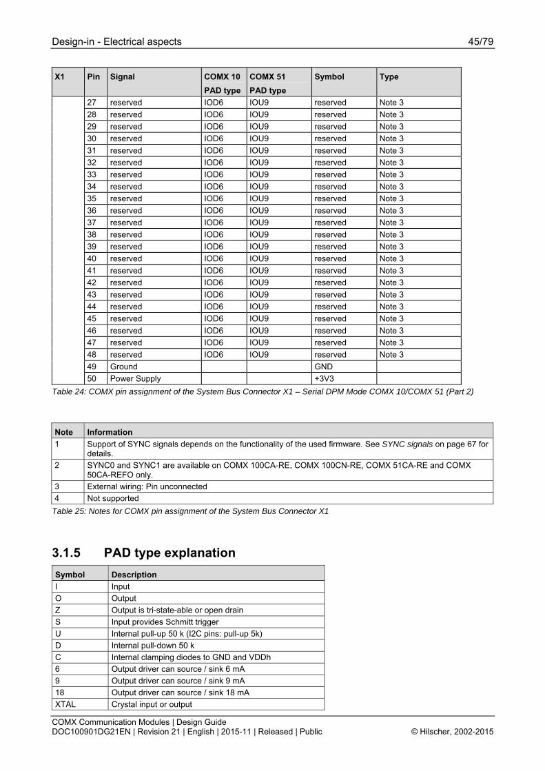
3.1.5 PAD type explanation Symbol Description I Input O Output Z Output is tri-state-able or open drain S Input provides Schmitt trigger U Internal pull-up 50 k (I2C pins: pull-up 5k) D Internal pull-down 50 k C Internal clamping diodes to GND and VDDh 6 Output driver can source / sink 6 mA 9 Output driver can source / sink 9 mA 18 Output driver can source / sink 18 mA XTAL Crystal input or output
Design-in - Electrical aspects 46/79
COMX Communication Modules | Design Guide DOC100901DG21EN | Revision 21 | English | 2015-11 | Released | Public © Hilscher, 2002-2015
Symbol Description USB USB pad PHY PHY pad ANA Analog pin PWR 1.5V (Core) or 3.3V /I/O) GND Digital ground (0V) APWR Analog power (1.5V or 3.3V) AGND Analog ground (0V)
Table 26: PAD Type Explanation
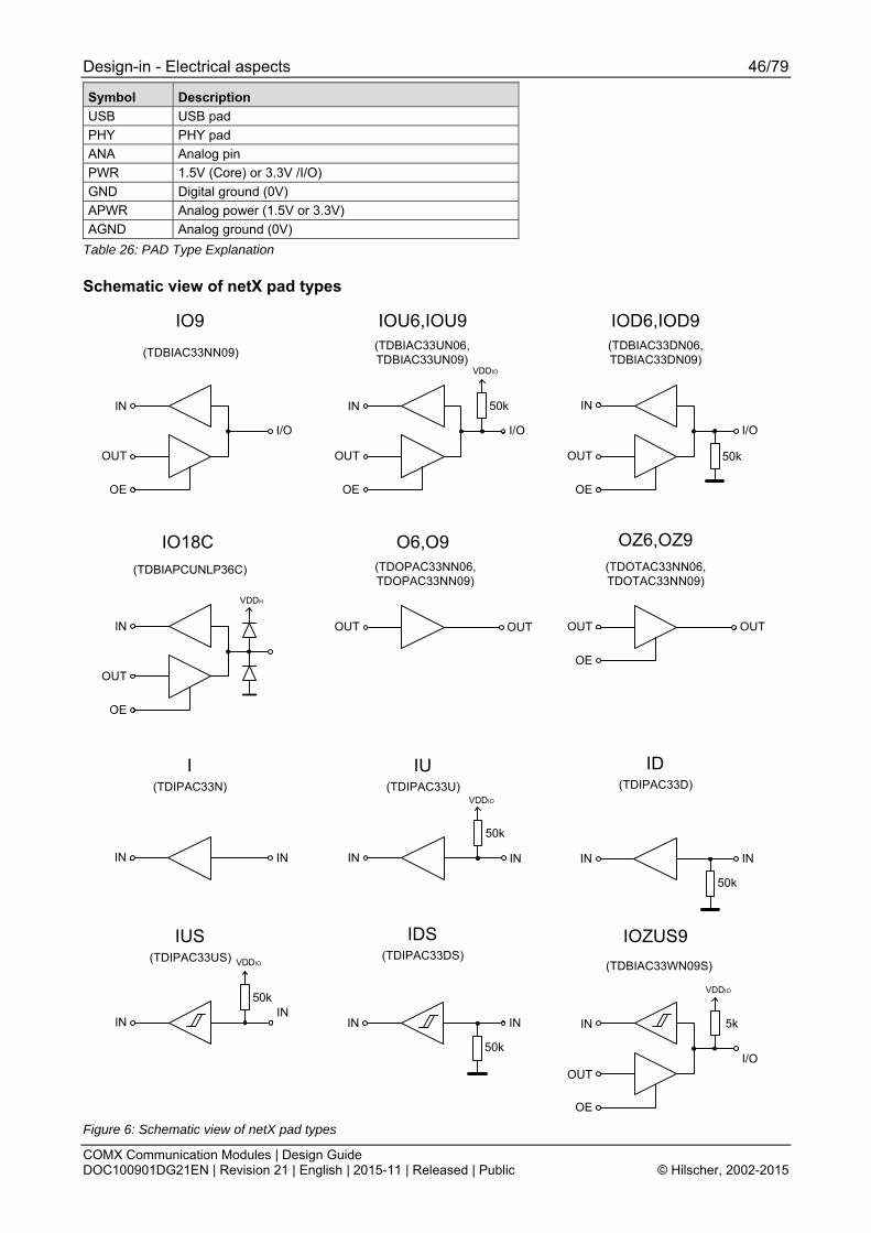
Schematic view of netX pad types
IO9
OUT
OE
IN
I/O
50k
IOU6,IOU9
VDDIO
50k
IN
50k
VDDIO
IN
IU
OUT
OE
IN
I/O
IOD6,IOD9
IN
ID
50k
IN
OUT
OE
IN 5k
IOZUS9
VDDIO
OUT
OE
IN
I/O
(TDBIAC33NN09) (TDBIAC33UN06,TDBIAC33UN09)
(TDBIAC33DN06,TDBIAC33DN09)
OUT OUT
O6,O9
OUT
OE
OUT
OZ6,OZ9(TDOPAC33NN06,TDOPAC33NN09)
(TDOTAC33NN06,TDOTAC33NN09)
(TDBIAC33WN09S)
(TDIPAC33U) (TDIPAC33D)
I/O
IN
50k
VDDIO
IN
IUS
IN
IDS
50k
IN
(TDIPAC33US) (TDIPAC33DS)
I(TDIPAC33N)
IN IN
OUT
OE
IN
IO18C
VDDH
(TDBIAPCUNLP36C)
Figure 6: Schematic view of netX pad types
Design-in - Electrical aspects 47/79
COMX Communication Modules | Design Guide DOC100901DG21EN | Revision 21 | English | 2015-11 | Released | Public © Hilscher, 2002-2015
3.1.6 Signal overview and pin assignment of the fieldbus connector X2 on COMX CN
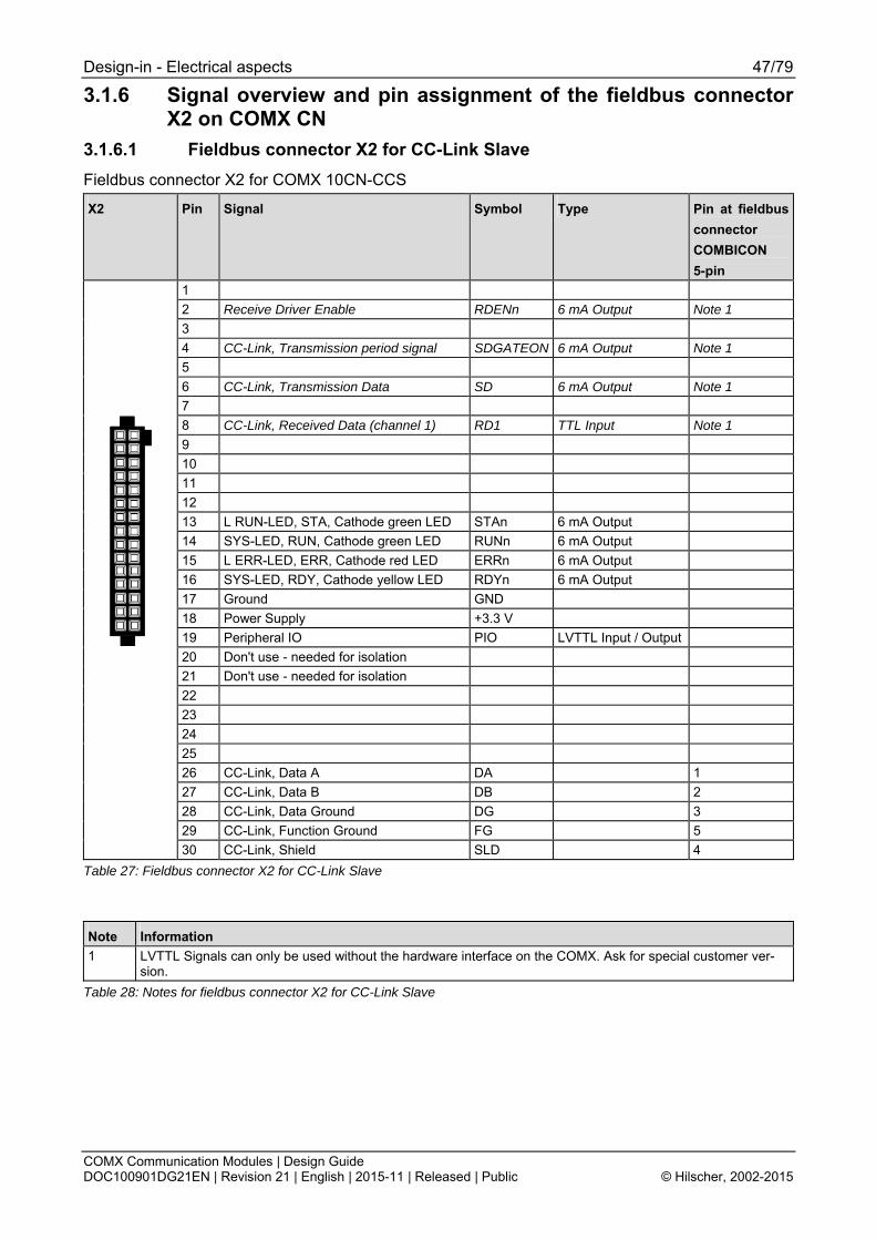
3.1.6.1 Fieldbus connector X2 for CC-Link Slave Fieldbus connector X2 for COMX 10CN-CCS
X2 Pin Signal Symbol Type Pin at fieldbusconnector COMBICON 5-pin
1 2 Receive Driver Enable RDENn 6 mA Output Note 1 3 4 CC-Link, Transmission period signal SDGATEON 6 mA Output Note 1 5 6 CC-Link, Transmission Data SD 6 mA Output Note 1 7 8 CC-Link, Received Data (channel 1) RD1 TTL Input Note 1 9 10 11 12 13 L RUN-LED, STA, Cathode green LED STAn 6 mA Output 14 SYS-LED, RUN, Cathode green LED RUNn 6 mA Output 15 L ERR-LED, ERR, Cathode red LED ERRn 6 mA Output 16 SYS-LED, RDY, Cathode yellow LED RDYn 6 mA Output 17 Ground GND 18 Power Supply +3.3 V 19 Peripheral IO PIO LVTTL Input / Output 20 Don't use - needed for isolation 21 Don't use - needed for isolation 22 23 24 25 26 CC-Link, Data A DA 1 27 CC-Link, Data B DB 2 28 CC-Link, Data Ground DG 3 29 CC-Link, Function Ground FG 5
30 CC-Link, Shield SLD 4 Table 27: Fieldbus connector X2 for CC-Link Slave
Note Information 1 LVTTL Signals can only be used without the hardware interface on the COMX. Ask for special customer ver-
sion. Table 28: Notes for fieldbus connector X2 for CC-Link Slave
Design-in - Electrical aspects 48/79
COMX Communication Modules | Design Guide DOC100901DG21EN | Revision 21 | English | 2015-11 | Released | Public © Hilscher, 2002-2015
3.1.6.2 Fieldbus Connector X2 for CANopen-Master/-Slave Fieldbus connector X2 for COMX 10CN-COS and COMX 100CN-CO
X2 Pin Signal Symbol Type Pin at Fieldbusconnector DSub 9, male
1 2 3 4 5 6 7 CAN, Receive Data CAN_RX1 LVTTL Input Note 1 8 9 CAN, Transmit Data CAN_TX1 LVTTL Output Note 1 10 11 12 13 COM-LED, STA, Cathode green LED STAn 4 mA Output Note 2 14 SYS-LED, RUN, Cathode green LED RUNn 4 mA Output 15 COM-LED, ERR, Cathode red LED ERRn 4 mA Output 16 SYS-LED, RDY, Cathode yellow LED RDYn 4 mA Output 17 Ground GND 18 Power Supply +3.3 V 19 Peripheral IO PIO LVTTL Input / Output 20 Don't use - needed for isolation 21 Don't use - needed for isolation 22 23 CAN_H Bus line CAN_H ISO 11898 7 24 25 26 CAN Ground CAN_GND 3 27 28 29 CAN_L Bus line CAN_L ISO 11898 2
30 Table 29: Fieldbus connector X2 for CANopen-Master/-Slave
Note Information 1 LVTTL Signals can only be used without the hardware interface on the COMX. Ask for special customer ver-
sion. 2 Green LED for COMX 100CN-CO
Table 30: Notes for fieldbus connector X2 for CANopen-Master/-Slave
Design-in - Electrical aspects 49/79
COMX Communication Modules | Design Guide DOC100901DG21EN | Revision 21 | English | 2015-11 | Released | Public © Hilscher, 2002-2015
3.1.6.3 Fieldbus Connector X2 for DeviceNet-Master/-Slave Fieldbus connector X2 for COMX 10CN-DNS and COMX 100CN-DN
X2 Pin Signal Symbol Type Pin at Fieldbusconnector COMBICON 5-pin
1 2 3 4 5 6 7 CAN, Receive Data CAN_RX1 LVTTL Input Note 1 8 9 CAN, Transmit Data CAN_TX1 LVTTL Output Note 1 10 11 CAN, Power Fail CAN_PF1 LVTTL Input Note 1 12 13 MNS-LED, active low, Cathode green
LED MNS_CGn 4 mA Output
14 RUN-LED, RUN, Cathode green LED RUNn 4 mA Output 15 MNS-LED, active low, Cathode red
LED MNS_CRn 4 mA Output
16 SYS-LED, RDY, Cathode yellow LED RDYn 4 mA Output 17 Ground GND 18 Power Supply +3.3 V 19 Peripheral IO PIO LVTTL Input / Output 20 Don't use - needed for isolation 21 Don't use - needed for isolation 22 23 24 25 26 Reference potential DeviceNet V- 1 27 CAN Low-Signal CAN_L 2 28 Shield Drain 3 29 CAN High-Signal CAN_H 4
30 +24V Power Supply DeviceNet V+ 5 Table 31: Fieldbus connector X2 for DeviceNet-Master/-Slave
Note Information 1 LVTTL Signals can only be used without the hardware interface on the COMX. Ask for special customer ver-
sion. Table 32: Notes for fieldbus connector X2 for DeviceNet-Master/-Slave
Design-in - Electrical aspects 50/79
COMX Communication Modules | Design Guide DOC100901DG21EN | Revision 21 | English | 2015-11 | Released | Public © Hilscher, 2002-2015
3.1.6.4 Fieldbus Connector X2 for PROFIBUS-Master/-Slave Fieldbus connector X2 for COMX 10CN-DPS and COMX 100CN-DP
X2 Pin Signal Symbol Type Pin at Fieldbusconnector DSub-9, female
1 PROFIBUS, Receive Data PB_RX LVTTL Input Note 1 2 3 PROFIBUS, Transmit Data PB_TX LVTTL Output Note 1 4 5 PROFIBUS, Enable Bus Driver PB_ENB LVTTL Output Note 1 6 7 8 9 10 11 12 13 COM-LED, STA, Cathode green LED
(COMX) STAn 4 mA Output Note 2
14 SYS-LED, RUN, Cathode green LED RUNn 4 mA Output 15 COM-LED, ERR, Cathode red LED ERRn 4 mA Output 16 SYS-LED, RDY, Cathode yellow LED RDYn 4 mA Output 17 Ground GND 18 Power Supply +3.3 V 19 Peripheral IO PIO LVTTL Input / Output 20 Don't use - needed for isolation 21 Don't use - needed for isolation 22 Reference potential DGND 5 23 Control CNTR-P LVTTL 4 24 25 Receive / Send Data-N RXD/TXD-N RS 485 8 26 Receive / Send Data-P RXD/TXD-P RS 485 3 27 28 29 Positive power supply VP + 5V 6
30 Table 33: Fieldbus connector X2 for PROFIBUS-Master/-Slave
Note Information 1 LVTTL Signals can only be used without the hardware interface on the COMX. Ask for special customer ver-
sion. 2 Green LED for COMX 100CN-DP
Table 34: Notes for fieldbus connector X2 for PROFIBUS-Master/-Slave
Design-in - Electrical aspects 51/79
COMX Communication Modules | Design Guide DOC100901DG21EN | Revision 21 | English | 2015-11 | Released | Public © Hilscher, 2002-2015
3.1.6.5 Fieldbus Connector X2 for Real Time Ethernet Fieldbus connector X2 for COMX 51CN-RE and COMX 100CN-RE:
X2 Pin Signal Symbol Type Pin at Fieldbusconnector RJ45
1 Link0-LED Cathode green, active low LINK0_CGn 4 mA Output 2 TX/RX0-LED Cathode yellow, active
low TX/RX0_CYn 4 mA Output
3 Link1-LED Cathode green, active low LINK1_CGn 4 mA Output 4 TX/RX1-LED Cathode yellow, active
low TX/RX1_CYn 4 mA Output
5 Transmit Data Positive Channel 0 CH0_TXP 1A 6 Transmit Data Negative Channel 0 CH0_TXN 2A 7 Transmit Center Tap Channel 0 CH0_TXC 4A 8 Ground GND 9 Receive Data Positive Channel 0 CH0_RXP 3A 10 Receive Data Negative Channel 0 CH0_RXN 6A 11 Receive Center Tap Channel 0 CH0_RXC 5A 12 Ground GND 13 Transmit Data Positive Channel 1 CH1_TXP 1B 14 Transmit Data Negative Channel 1 CH1_TXN 2B 15 Transmit Center Tap Channel 1 CH1_TXC 4B 16 Ground GND 17 Receive Data Positive Channel 1 CH1_RXP 3B 18 Receive Data Negative Channel 1 CH1_RXN 6B 19 Receive Center Tap Channel 1 CH1_RXC 5B 20 Ground GND 21 COM0-LED Cathode red, active low COM0_CRn 4 mA Output 22 COM0-LED Cathode green, active low COM0_CGn 4 mA Output 23 COM1-LED Cathode red, active low COM1_CRn 4 mA Output 24 COM1-LED Cathode green, active low COM1_CGn 4 mA Output 25 SYS-LED, RDY, Cathode yellow LED RDYn 4 mA Output 26 SYS-LED, RUN, Cathode green LED RUNn 4 mA Output 27 Peripheral IO PIO LVTTL Input / Output 28 not connected 29 not connected
30 not connected Table 35: Fieldbus connector X2 for Real-Time Ethernet
The pin layout is designed to fit for a RJ45 connector with integrated transformers, LEDs and ter-mination. Suggested part: ! 203313, ERNI or ! J8064D628ANL, Pulse
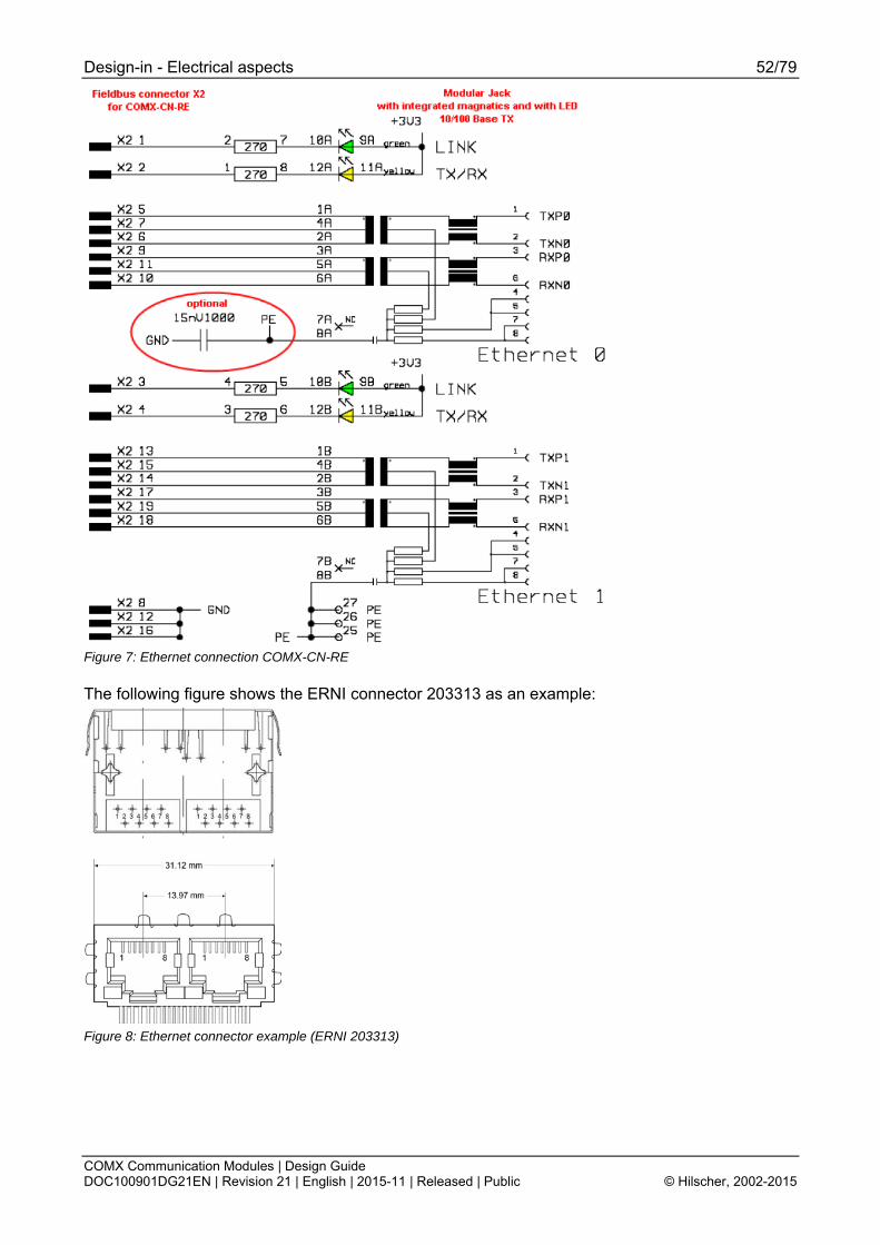
Design-in - Electrical aspects 52/79
COMX Communication Modules | Design Guide DOC100901DG21EN | Revision 21 | English | 2015-11 | Released | Public © Hilscher, 2002-2015
Figure 7: Ethernet connection COMX-CN-RE
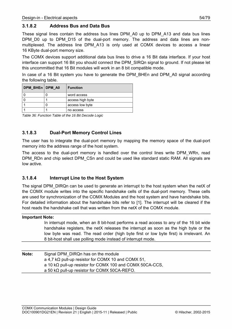
The following figure shows the ERNI connector 203313 as an example:
Figure 8: Ethernet connector example (ERNI 203313)
Design-in - Electrical aspects 53/79
COMX Communication Modules | Design Guide DOC100901DG21EN | Revision 21 | English | 2015-11 | Released | Public © Hilscher, 2002-2015
3.1.7 Common signals of the host interface 3.1.7.1 Power supply of the COMX modules Only a single 3.3 V operation voltage is needed for the COMX Module. The voltage must be regu-lated and can have a tolerance of ±5 % (3.135 ... 3.465 V) and must be connected twice to the sys-tem bus connector X1. To avoid EMI problems we suggest using bypass capacitors in the power supply path. All other special voltages required on the COMX Module are generated by on board DC/DC converter. A watchdog circuit on all COMX Modules supervises the voltage and the microprocessor. If the voltage decreases below the voltage reset level of typically 2.93 V (2.85 ... 3.00 V) the COMX Module are hold in reset state. If the voltage exceeds the reset voltage threshold the COMX Mod-ule will begin with the power up sequence. To avoid problems with the power supply we recommend using a voltage of 3.3 V. So the operation will be in the safe range of voltage operation area and short voltage drops, spikes and noise will not cause any reset conditions. The maximum current depends on netJACK module type. For specific current values see section Technical data on page 68.
3.1.7.2 RESET signal It is possible to reset the COMX Module by the extra reset signal DPM_RESETn. For operation of the COMX Module it is important to switch the signal DPM_RESETn to high level. Then the COMX Module begins with the program execution and initialization. This power up time is different for each COMX Module. Normally, the time is about less than two seconds. The COMX Module is in reset state when the signal DPM_RESETn has a static low level. To reset the COMX Module the DPM_RESETn signal must be low for more than 10 µs.
Note During Reset all signals of the dual-port memory are configured as inputs! The output level could be floating. If the host system needs a stable level a pull-up or pull-down re-sistor is required on the host board. The COMX has pull-up resistors on board for the output lines DPM_BUSYn and DPM_DIRQn.
3.1.8 Signals of the host interface Parallel dual-port memory mode 3.1.8.1 The dual-port memory bus of COMX The communication for all input and output data and control commands between the COMX and the host system are exchanged over the dual-port memory. The communication is not compatible to the COM-A/-B-/C devices. The address map of the dual-port memory is different. From host system side, the dual-port memory looks like static RAM. The dual-port memory size of the COMX module depends on the COMX module type, see section Host interface overview: Dual-port memory sizes and modes on page 39. Only a few signals are used to control the access to the dual-port memory. The maximum driving capability for the data lines is 8 mA (COMX 50, COMX 100) respectively 6 mA (COMX 10) and 9 mA (COMX 51). To avoid data loss through simultaneous access at the same memory cell, it is necessary to use the DPM_BUSYn signal. See section BUSY Line to the Host System on page 55. Please refer to the special documents for the basic description of the data model and communica-tion methods with devices based on the netX.
Design-in - Electrical aspects 54/79
COMX Communication Modules | Design Guide DOC100901DG21EN | Revision 21 | English | 2015-11 | Released | Public © Hilscher, 2002-2015
3.1.8.2 Address Bus and Data Bus These signal lines contain the address bus lines DPM_A0 up to DPM_A13 and data bus lines DPM_D0 up to DPM_D15 of the dual-port memory. The address and data lines are non-multiplexed. The address line DPM_A13 is only used at COMX devices to access a linear 16 KByte dual-port memory size. The COMX devices support additional data bus lines to drive a 16 Bit data interface. If your host interface can support 16 Bit you should connect the DPM_SIRQn signal to ground. If not please let this uncommitted that 16 Bit modules will work in an 8 bit compatible mode. In case of a 16 Bit system you have to generate the DPM_BHEn and DPM_A0 signal according the following table.
DPM_BHEn DPM_A0 Function
0 0 word access 0 1 access high byte 1 0 access low byte 1 1 no access
Table 36: Function Table of the 16 Bit Decode Logic
3.1.8.3 Dual-Port Memory Control Lines The user has to integrate the dual-port memory by mapping the memory space of the dual-port memory into the address range of the host system. The access to the dual-port memory is handled over the control lines write DPM_WRn, read DPM_RDn and chip select DPM_CSn and could be used like standard static RAM. All signals are low active.
3.1.8.4 Interrupt Line to the Host System The signal DPM_DIRQn can be used to generate an interrupt to the host system when the netX of the COMX module writes into the specific handshake cells of the dual-port memory. These cells are used for synchronization of the COMX Modules and the host system and have handshake bits. For detailed information about the handshake bits refer to [1]. The interrupt will be cleared if the host reads the handshake cell that was written from the netX of the COMX module.
Important Note: In interrupt mode, when an 8 bit-host performs a read access to any of the 16 bit wide handshake registers, the netX releases the interrupt as soon as the high byte or the low byte was read. The read order (high byte first or low byte first) is irrelevant. An 8 bit-host shall use polling mode instead of interrupt mode.
Note: Signal DPM_DIRQn has on the module a 4,7 kΩ pull-up resistor for COMX 10 and COMX 51, a 10 kΩ pull-up resistor for COMX 100 and COMX 50CA-CCS, a 50 kΩ pull-up resistor for COMX 50CA-REFO.
Design-in - Electrical aspects 55/79
COMX Communication Modules | Design Guide DOC100901DG21EN | Revision 21 | English | 2015-11 | Released | Public © Hilscher, 2002-2015
3.1.8.5 BUSY Line to the Host System The signal BUSYn is used to insert wait states into a current access from host system to a COMX module. When the signal is active the host must hold on the current transfer. The timing diagram is described in section Timing Diagram parallel Dual-Port Memory Interface on page 56.
Important Note 1: Avoid dual-port memory access errors It is mandatory that the host CPU always uses the DPM_BUSY signal, otherwise this results in wrong data read from the dual-port memory or dual-port memory write accesses are being ignored. This does not affect COMX10 and COMX51 modules! ! The maximum value for accesses cannot be specified. ! For maximum performance, the DPM_BUSY signal must always be evaluated by the host CPU. ! If you use a host CPU that can not use the DPM_BUSY signal, then contact our technical support.
Note 2: The COMX has a 10 kΩ pull-up resistor on board for the output line DPM_BUSYn
3.1.8.6 Interfacing to the Dual-Port Memory for COMX If you connect the host system to the dual-port memory of the COMX Module you have to know some details of the functional working of the netX. All accesses to the dual-port memory are synchronized to the netX clock and will be then trans-lated into an internal access cycle. This needs some time. To manage the access timing the DPM_BUSYn signal is generated to signal the host system to lengthen the current access cycle until the data could be written or the read data is valid. An access cycle is started when the chip select line DPM_CSn and read DPM_RDn or write DPM_WRn line are active. The address line must be stable during the complete cycle. It is not possible to switch the address lines during a cycle (no burst access). Moreover there must be a recovery time during two accesses. For further details please refer the following timing diagrams.
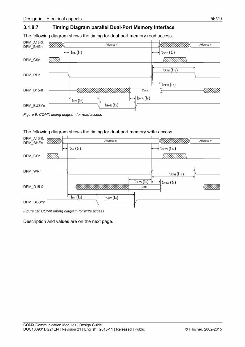
Design-in - Electrical aspects 56/79
COMX Communication Modules | Design Guide DOC100901DG21EN | Revision 21 | English | 2015-11 | Released | Public © Hilscher, 2002-2015
3.1.8.7 Timing Diagram parallel Dual-Port Memory Interface The following diagram shows the timing for dual-port memory read access.
Figure 9: COMX timing diagram for read access
The following diagram shows the timing for dual-port memory write access.
Figure 10: COMX timing diagram for write access
Description and values are on the next page.

Design-in - Electrical aspects 57/79
COMX Communication Modules | Design Guide DOC100901DG21EN | Revision 21 | English | 2015-11 | Released | Public © Hilscher, 2002-2015
The following table gives the values for the timing parameters for COMX 10 modules using the netX 10 chip, for COMX 50 modules using the netX 50 chip, for COMX 51 modules using the netX 51 chip and for COMX 100 using the netX 100 chip. For exchangeability of COMX 10, COMX 50, COMX 51 and COMX 100 communication modules use the values of column Common of Table 37.
Symbol Description COMX 10netX 10
COMX 50 netX 50
COMX 100 netX 100
COMX 51 netX 51
Com-mon
t1 tAS min. Minimum address setup time 0 ns 1.9 ns 0 ns 0 ns 2 ns t2 tBV max. Maximum Time from cycle start
until BUSYn signal is valid 5.7 ns 35.5 ns 30 ns 5,7 ns 40 ns
tBAR typ. Typical BUSY active time (read ac-cess) See note 2
- 50 ns 80 ns - - t3
tBAR max. Maximum BUSY active time (read access) See important note 1
68 ns - - 68 ns -
tBAW min. Minimum BUSY active time (write access)
0 ns 0 ns 0 ns 0 ns 0 ns t4
tBAW max. Maximum BUSY active time (write access) See important note 1
68 ns - - 68 ns -
t5 tDVR min. Minimum Time between valid data bus signals and rising edge of BUSYn signal
7,8 ns 8.3 ns 5 ns 7,8 ns 5 ns
t6 tDSW min. Minimum setup time for write data 10.8 ns 12.1 ns 25 ns 12.8 ns 25 ns t7 tDHR min. Minimum read data hold time 2.1 ns 1.5 ns 0 ns 2.1 ns 0 ns t8 tDHW min. Minimum hold time for write data 0.8 ns 0 ns 0 ns 2.8 ns 2.8 ns t9 tAHR min. Minimum address hold time 0 ns 0 ns 0 ns 0 ns 0 ns t10 tAHW min. Minimum address hold time 0.9 ns 0 ns 0 ns 2.9 ns 2.9 ns t11 tRWI Minimum inactive time for RDn or
WRn 10.5 ns 10 ns 10 ns 12.5 ns 12.5 ns
Table 37: Symbols for COMX Timing Diagram for Read and Write Access
Important Note 1:
Avoid dual-port memory access errors It is mandatory that the host CPU always uses the DPM_BUSYn signal, otherwise this results in wrong data read from the dual-port memory or dual-port memory write accesses are ignored. This does not affect COMX10 und COMX51! ! The maximum value for accesses cannot be specified. ! For maximum performance, the DPM_BUSYn signal must always be evaluated by the host CPU. ! If you use a host CPU that cannot use the DPM_BUSYn signal, then contact our technical support.
Note 2: The value for tBAR typ. (t3 typ.) depends on the used firmware/application on the netX.
Note 3: DPM_BHEn is only used for 16 bit interface.
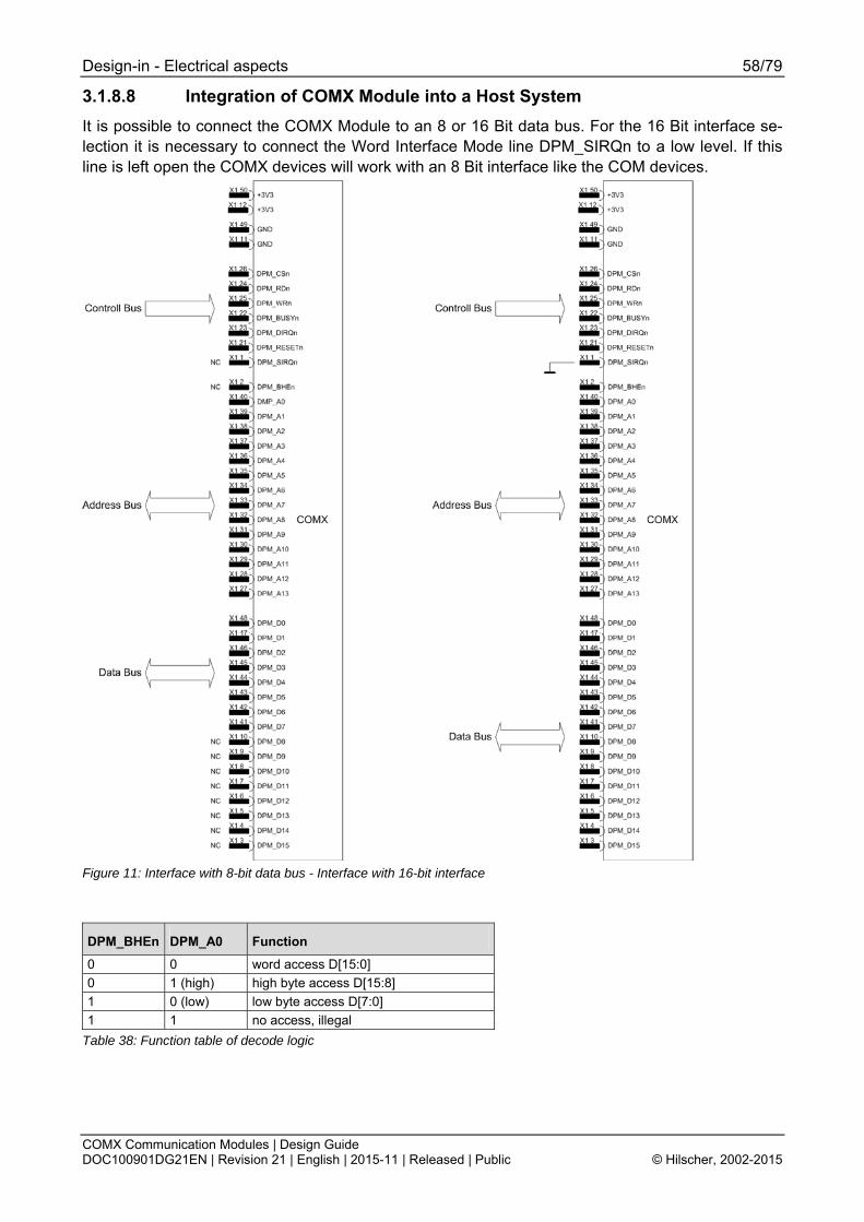
Design-in - Electrical aspects 58/79
COMX Communication Modules | Design Guide DOC100901DG21EN | Revision 21 | English | 2015-11 | Released | Public © Hilscher, 2002-2015
3.1.8.8 Integration of COMX Module into a Host System It is possible to connect the COMX Module to an 8 or 16 Bit data bus. For the 16 Bit interface se-lection it is necessary to connect the Word Interface Mode line DPM_SIRQn to a low level. If this line is left open the COMX devices will work with an 8 Bit interface like the COM devices.
Figure 11: Interface with 8-bit data bus - Interface with 16-bit interface
DPM_BHEn DPM_A0 Function
0 0 word access D[15:0] 0 1 (high) high byte access D[15:8] 1 0 (low) low byte access D[7:0] 1 1 no access, illegal
Table 38: Function table of decode logic
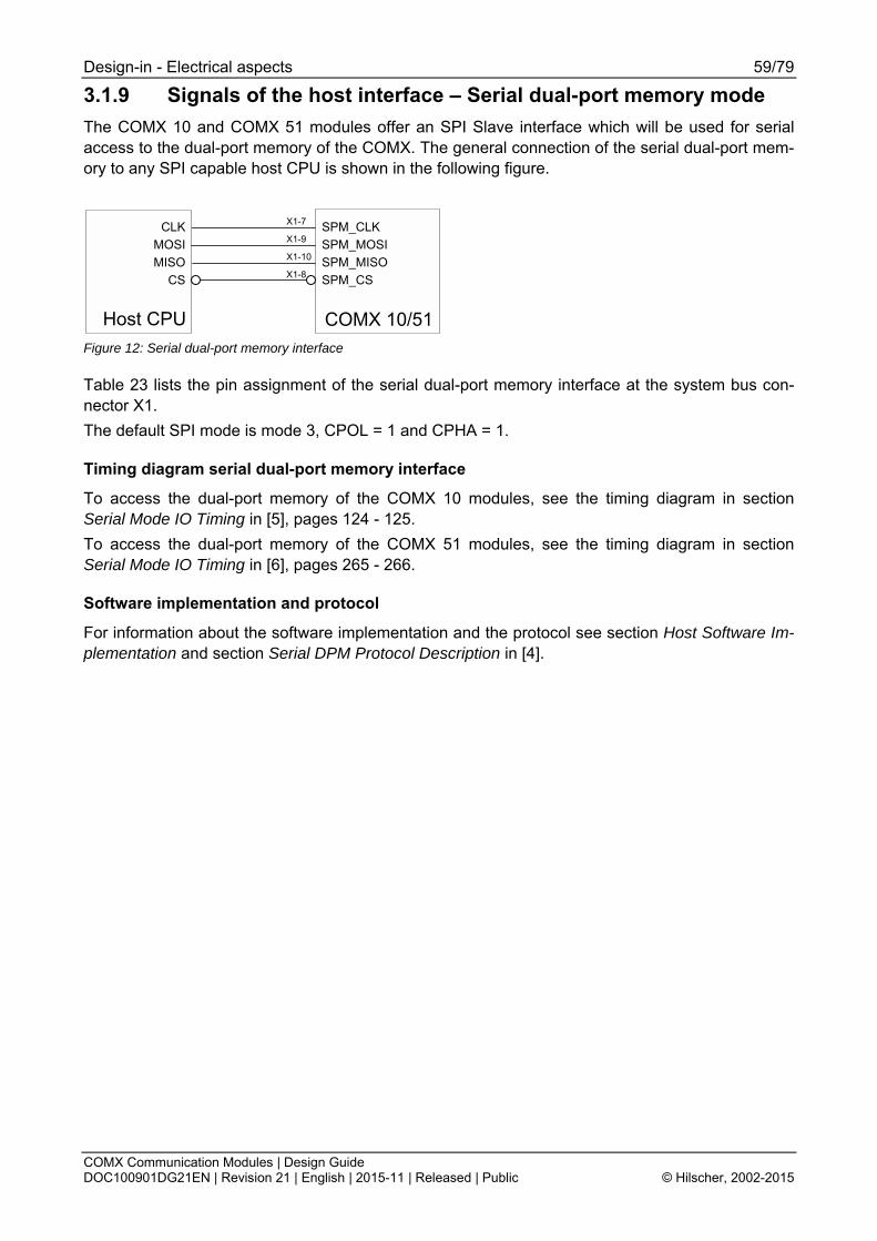
Design-in - Electrical aspects 59/79
COMX Communication Modules | Design Guide DOC100901DG21EN | Revision 21 | English | 2015-11 | Released | Public © Hilscher, 2002-2015
3.1.9 Signals of the host interface Serial dual-port memory mode The COMX 10 and COMX 51 modules offer an SPI Slave interface which will be used for serial access to the dual-port memory of the COMX. The general connection of the serial dual-port mem-ory to any SPI capable host CPU is shown in the following figure.
Host CPU COMX 10/51
CLKMOSIMISO
CS
SPM_CLKSPM_MOSISPM_MISOSPM_CS
X1-7
X1-9
X1-10
X1-8
Figure 12: Serial dual-port memory interface
Table 23 lists the pin assignment of the serial dual-port memory interface at the system bus con-nector X1. The default SPI mode is mode 3, CPOL = 1 and CPHA = 1.
Timing diagram serial dual-port memory interface
To access the dual-port memory of the COMX 10 modules, see the timing diagram in section Serial Mode IO Timing in [5], pages 124 - 125. To access the dual-port memory of the COMX 51 modules, see the timing diagram in section Serial Mode IO Timing in [6], pages 265 - 266.
Software implementation and protocol
For information about the software implementation and the protocol see section Host Software Im-plementation and section Serial DPM Protocol Description in [4].

Design-in - Electrical aspects 60/79
COMX Communication Modules | Design Guide DOC100901DG21EN | Revision 21 | English | 2015-11 | Released | Public © Hilscher, 2002-2015
3.2 Fieldbus interface Figure 13 shows the connections of the pins of X2 and the pins of the Fieldbus connector.
COMX Pin of FieldbusConnector
Figure 13: Fieldbus interface connections
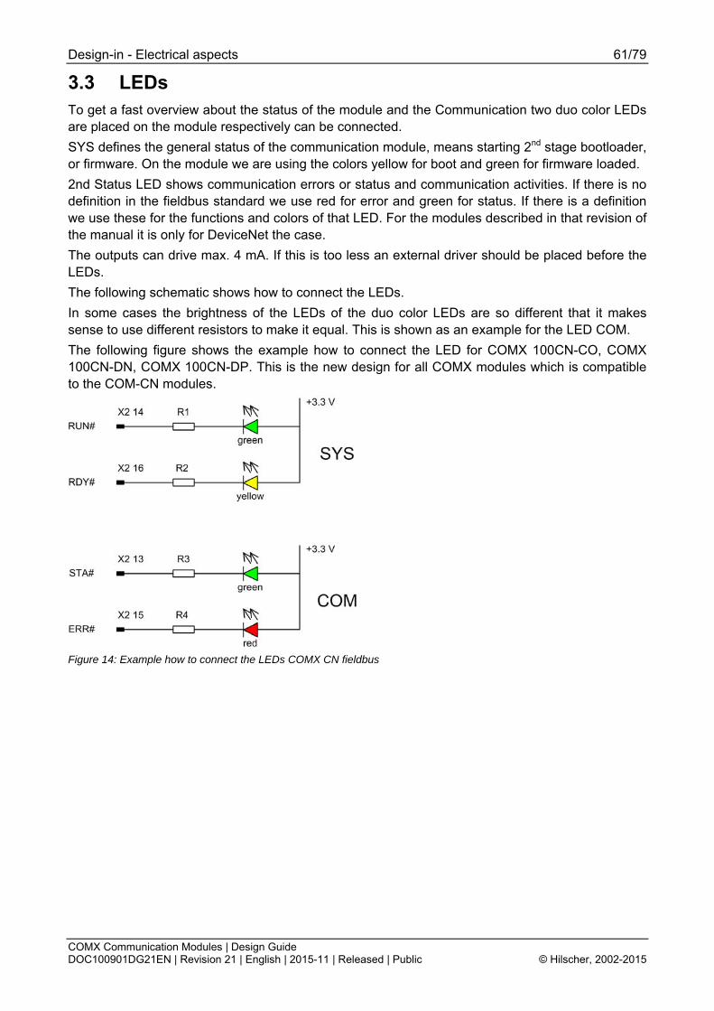
Design-in - Electrical aspects 61/79
COMX Communication Modules | Design Guide DOC100901DG21EN | Revision 21 | English | 2015-11 | Released | Public © Hilscher, 2002-2015
3.3 LEDs To get a fast overview about the status of the module and the Communication two duo color LEDs are placed on the module respectively can be connected. SYS defines the general status of the communication module, means starting 2nd stage bootloader, or firmware. On the module we are using the colors yellow for boot and green for firmware loaded. 2nd Status LED shows communication errors or status and communication activities. If there is no definition in the fieldbus standard we use red for error and green for status. If there is a definition we use these for the functions and colors of that LED. For the modules described in that revision of the manual it is only for DeviceNet the case. The outputs can drive max. 4 mA. If this is too less an external driver should be placed before the LEDs. The following schematic shows how to connect the LEDs. In some cases the brightness of the LEDs of the duo color LEDs are so different that it makes sense to use different resistors to make it equal. This is shown as an example for the LED COM. The following figure shows the example how to connect the LED for COMX 100CN-CO, COMX 100CN-DN, COMX 100CN-DP. This is the new design for all COMX modules which is compatible to the COM-CN modules.
Figure 14: Example how to connect the LEDs COMX CN fieldbus
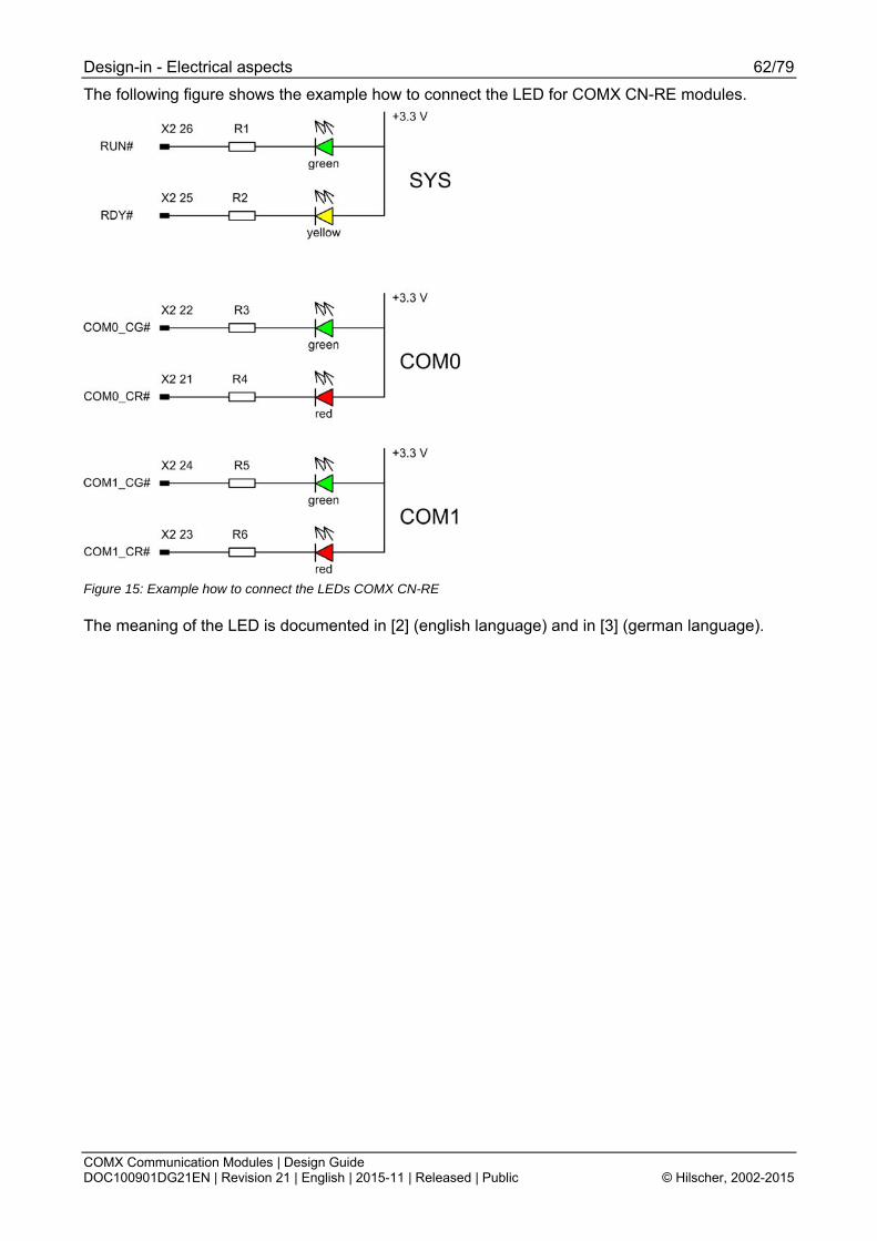
Design-in - Electrical aspects 62/79
COMX Communication Modules | Design Guide DOC100901DG21EN | Revision 21 | English | 2015-11 | Released | Public © Hilscher, 2002-2015
The following figure shows the example how to connect the LED for COMX CN-RE modules.
Figure 15: Example how to connect the LEDs COMX CN-RE
The meaning of the LED is documented in [2] (english language) and in [3] (german language).
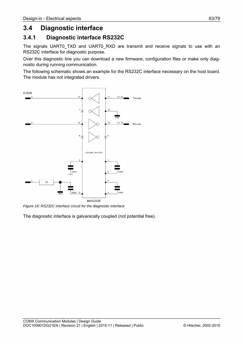
Design-in - Electrical aspects 63/79
COMX Communication Modules | Design Guide DOC100901DG21EN | Revision 21 | English | 2015-11 | Released | Public © Hilscher, 2002-2015
3.4 Diagnostic interface 3.4.1 Diagnostic interface RS232C The signals UART0_TXD and UART0_RXD are transmit and receive signals to use with an RS232C interface for diagnostic purpose. Over this diagnostic line you can download a new firmware, configuration files or make only diag-nostic during running communication. The following schematic shows an example for the RS232C interface necessary on the host board. The module has not integrated drivers.
Figure 16: RS232C interface circuit for the diagnostic interface
The diagnostic interface is galvanically coupled (not potential free).

Design-in - Electrical aspects 64/79
COMX Communication Modules | Design Guide DOC100901DG21EN | Revision 21 | English | 2015-11 | Released | Public © Hilscher, 2002-2015
3.4.2 Diagnostic interface USB The COMX modules have an USB port for diagnostic. The following figure shows the circuit for the USB interface.
Figure 17: USB interface circuit for the diagnostic interface
This USB interface is for the COMX modules from the following hardware revision:
Module Hardware revision Remark COMX 10CA-CCS 1 - COMX 10CN-CCS 1 - COMX 10CA-COS 1 - COMX 10CN-COS 1 - COMX 10CA-DNS 1 - COMX 10CN-DNS 1 - COMX 10CA-DPS 1 - COMX 10CN-DPS 1 - COMX 50CA-CCS 3 Firmware does not support USB COMX 50CA-REFO 2 - COMX 51CA-RE 1 - COMX 51CN-RE 1 - COMX 100CA-CO 4 - COMX 100CN-CO 3 - COMX 100CA-DN 4 - COMX 100CN-DN 3 - COMX 100CA-DP 4 - COMX 100CN-DP 3 - COMX 100CA-RE 7 - COMX 100CN-RE 2 - Table 39: Hardware revision of COMX modules with new USB interface
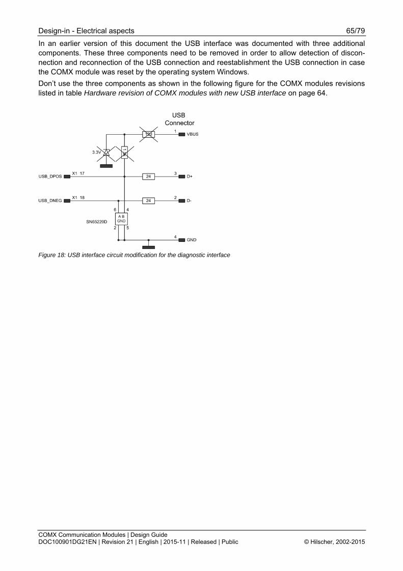
Design-in - Electrical aspects 65/79
COMX Communication Modules | Design Guide DOC100901DG21EN | Revision 21 | English | 2015-11 | Released | Public © Hilscher, 2002-2015
In an earlier version of this document the USB interface was documented with three additional components. These three components need to be removed in order to allow detection of discon-nection and reconnection of the USB connection and reestablishment the USB connection in case the COMX module was reset by the operating system Windows. Dont use the three components as shown in the following figure for the COMX modules revisions listed in table Hardware revision of COMX modules with new USB interface on page 64.
Figure 18: USB interface circuit modification for the diagnostic interface

Design-in - Electrical aspects 66/79
COMX Communication Modules | Design Guide DOC100901DG21EN | Revision 21 | English | 2015-11 | Released | Public © Hilscher, 2002-2015
The schematic for the USB interface for the COMX modules for older revisions is shown in the fol-lowing figure:
This USB interface is for the COMX modules up to the following hardware revision:
Module Hardware revision COMX 100CA-CO 3 COMX 100CN-CO 2 COMX 100CA-DN 3 COMX 100CN-DN 2 COMX 100CA-DP 3 COMX 100CN-DP 2 COMX 50CA-CCS 2 COMX 100CA-RE 6 COMX 100CN-RE 1 Table 40: Hardware revision of COMX modules with old USB interface
Design-in - Electrical aspects 67/79
COMX Communication Modules | Design Guide DOC100901DG21EN | Revision 21 | English | 2015-11 | Released | Public © Hilscher, 2002-2015
3.5 SYNC signals COMX modules for Real-Time Ethernet provide SYNC signals. The SYNC Signal has LVTTL level (3,3 V). A maximum load of 6 mA may not be exceeded. The SYNC signals can only be used if this is supported by the respective firmware, see table below.
Possible Destruction of the Device due to high current! Make sure that never two outputs drive against each other. Two outputs that drive against each other cause a too high current and result in device damage. This situation can happen for example, if the host system has an output signal connected to SYNC0 and a firmware is loaded that uses SYNC0 as output too.
It is also strongly recommended to keep the cable length for the SYNC signals below 50 mm and to take EMC aspects into account. In general, both SYNC signal lines can be used as input or output. The loaded firmware deter-mines if the signal is an input signal or output signal. The following table shows the meaning of the SYNC signals for the real-time Ethernet protocols currently offering SYNC signal support.
Protocol Signal IO_SYNC0 Input/Output
Signal IO_SYNC1 Input/Output
From Firm-ware Version
Remarks
EtherCAT Slave SYNC 0 Output
SYNC 1 Output
- Configurable
PROFINET IO Device
Bus cycle start (PROFINET IRT) Output
- 3.4.x.x -
sercos III Master External trigger to start bus cycle Input Rising edge
- 2.0.8.0 -
sercos III Slave CON_CLK Output
DIV_CLK Output
3.0.10.0 Configurable
Table 41: Meaning of the SYNC Signals for each Protocol
Note: A PROFINET IO certification for PROFINET IRT requires (mandatory) that the device offers the synchronization signal (SYNC0), in order to allow connecting an oscillo-scope. The host system (your product) must provide the SYNC0 signal!
For this purpose, connect the SYNC0 signal and ground of the system connector of the comX with a well accessible 2-pin connector.
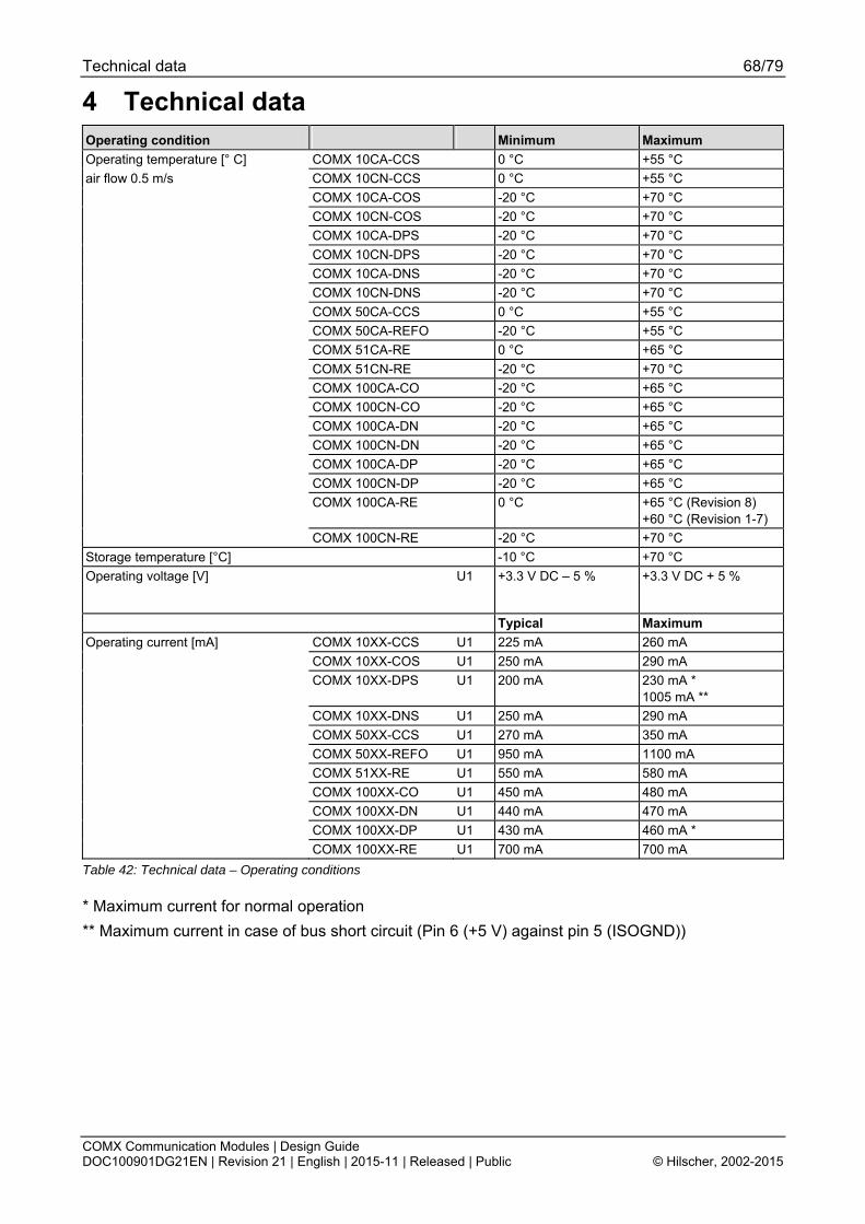
Technical data 68/79
COMX Communication Modules | Design Guide DOC100901DG21EN | Revision 21 | English | 2015-11 | Released | Public © Hilscher, 2002-2015
4 Technical data Operating condition Minimum Maximum Operating temperature [° C] COMX 10CA-CCS 0 °C +55 °C air flow 0.5 m/s COMX 10CN-CCS 0 °C +55 °C COMX 10CA-COS -20 °C +70 °C COMX 10CN-COS -20 °C +70 °C COMX 10CA-DPS -20 °C +70 °C COMX 10CN-DPS -20 °C +70 °C COMX 10CA-DNS -20 °C +70 °C COMX 10CN-DNS -20 °C +70 °C COMX 50CA-CCS 0 °C +55 °C COMX 50CA-REFO -20 °C +55 °C COMX 51CA-RE 0 °C +65 °C COMX 51CN-RE -20 °C +70 °C COMX 100CA-CO -20 °C +65 °C COMX 100CN-CO -20 °C +65 °C COMX 100CA-DN -20 °C +65 °C COMX 100CN-DN -20 °C +65 °C COMX 100CA-DP -20 °C +65 °C COMX 100CN-DP -20 °C +65 °C COMX 100CA-RE 0 °C +65 °C (Revision 8)
+60 °C (Revision 1-7) COMX 100CN-RE -20 °C +70 °C Storage temperature [°C] -10 °C +70 °C Operating voltage [V] U1 +3.3 V DC 5 % +3.3 V DC + 5 %
Typical Maximum Operating current [mA] COMX 10XX-CCS U1 225 mA 260 mA COMX 10XX-COS U1 250 mA 290 mA COMX 10XX-DPS U1 200 mA 230 mA *
1005 mA ** COMX 10XX-DNS U1 250 mA 290 mA COMX 50XX-CCS U1 270 mA 350 mA COMX 50XX-REFO U1 950 mA 1100 mA COMX 51XX-RE U1 550 mA 580 mA COMX 100XX-CO U1 450 mA 480 mA COMX 100XX-DN U1 440 mA 470 mA COMX 100XX-DP U1 430 mA 460 mA * COMX 100XX-RE U1 700 mA 700 mA Table 42: Technical data – Operating conditions
* Maximum current for normal operation ** Maximum current in case of bus short circuit (Pin 6 (+5 V) against pin 5 (ISOGND))
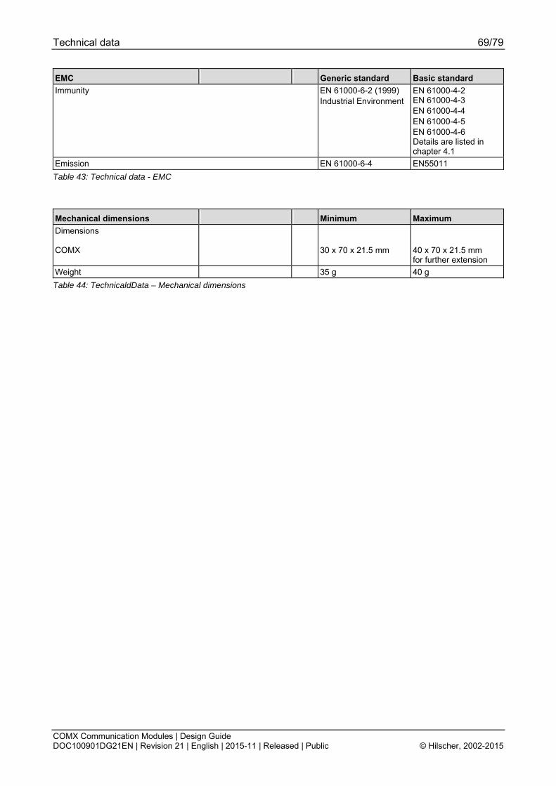
Technical data 69/79
COMX Communication Modules | Design Guide DOC100901DG21EN | Revision 21 | English | 2015-11 | Released | Public © Hilscher, 2002-2015
EMC Generic standard Basic standard Immunity EN 61000-6-2 (1999)
Industrial Environment
EN 61000-4-2 EN 61000-4-3 EN 61000-4-4 EN 61000-4-5 EN 61000-4-6 Details are listed in chapter 4.1
Emission EN 61000-6-4 EN55011 Table 43: Technical data - EMC
Mechanical dimensions Minimum Maximum Dimensions COMX
30 x 70 x 21.5 mm
40 x 70 x 21.5 mm for further extension
Weight 35 g 40 g Table 44: TechnicaldData – Mechanical dimensions
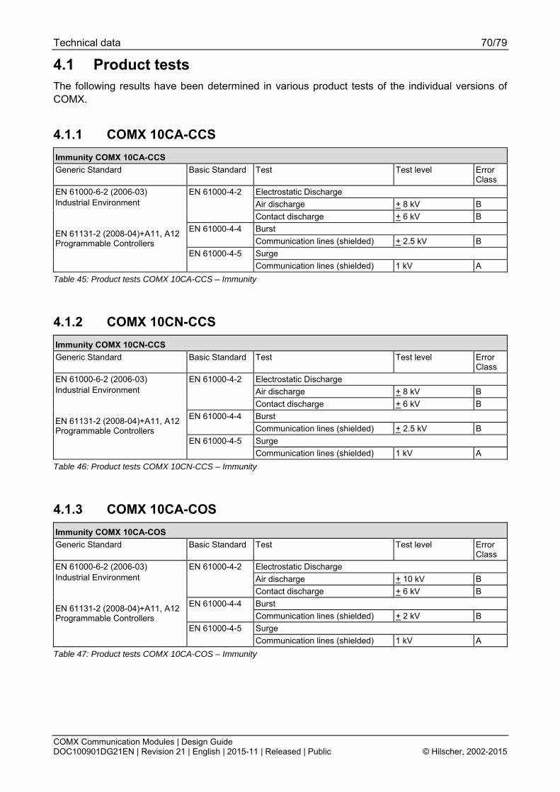
Technical data 70/79
COMX Communication Modules | Design Guide DOC100901DG21EN | Revision 21 | English | 2015-11 | Released | Public © Hilscher, 2002-2015
4.1 Product tests The following results have been determined in various product tests of the individual versions of COMX.
4.1.1 COMX 10CA-CCS Immunity COMX 10CA-CCS Generic Standard Basic Standard Test Test level Error
Class Electrostatic Discharge Air discharge + 8 kV B
EN 61000-4-2
Contact discharge + 6 kV B Burst EN 61000-4-4 Communication lines (shielded) + 2.5 kV B Surge
EN 61000-6-2 (2006-03) Industrial Environment EN 61131-2 (2008-04)+A11, A12 Programmable Controllers
EN 61000-4-5 Communication lines (shielded) 1 kV A
Table 45: Product tests COMX 10CA-CCS – Immunity
4.1.2 COMX 10CN-CCS Immunity COMX 10CN-CCS Generic Standard Basic Standard Test Test level Error
Class Electrostatic Discharge Air discharge + 8 kV B
EN 61000-4-2
Contact discharge + 6 kV B Burst EN 61000-4-4 Communication lines (shielded) + 2.5 kV B Surge
EN 61000-6-2 (2006-03) Industrial Environment EN 61131-2 (2008-04)+A11, A12 Programmable Controllers
EN 61000-4-5 Communication lines (shielded) 1 kV A
Table 46: Product tests COMX 10CN-CCS – Immunity
4.1.3 COMX 10CA-COS Immunity COMX 10CA-COS Generic Standard Basic Standard Test Test level Error
Class Electrostatic Discharge Air discharge + 10 kV B
EN 61000-4-2
Contact discharge + 6 kV B Burst EN 61000-4-4 Communication lines (shielded) + 2 kV B Surge
EN 61000-6-2 (2006-03) Industrial Environment EN 61131-2 (2008-04)+A11, A12 Programmable Controllers
EN 61000-4-5 Communication lines (shielded) 1 kV A
Table 47: Product tests COMX 10CA-COS – Immunity
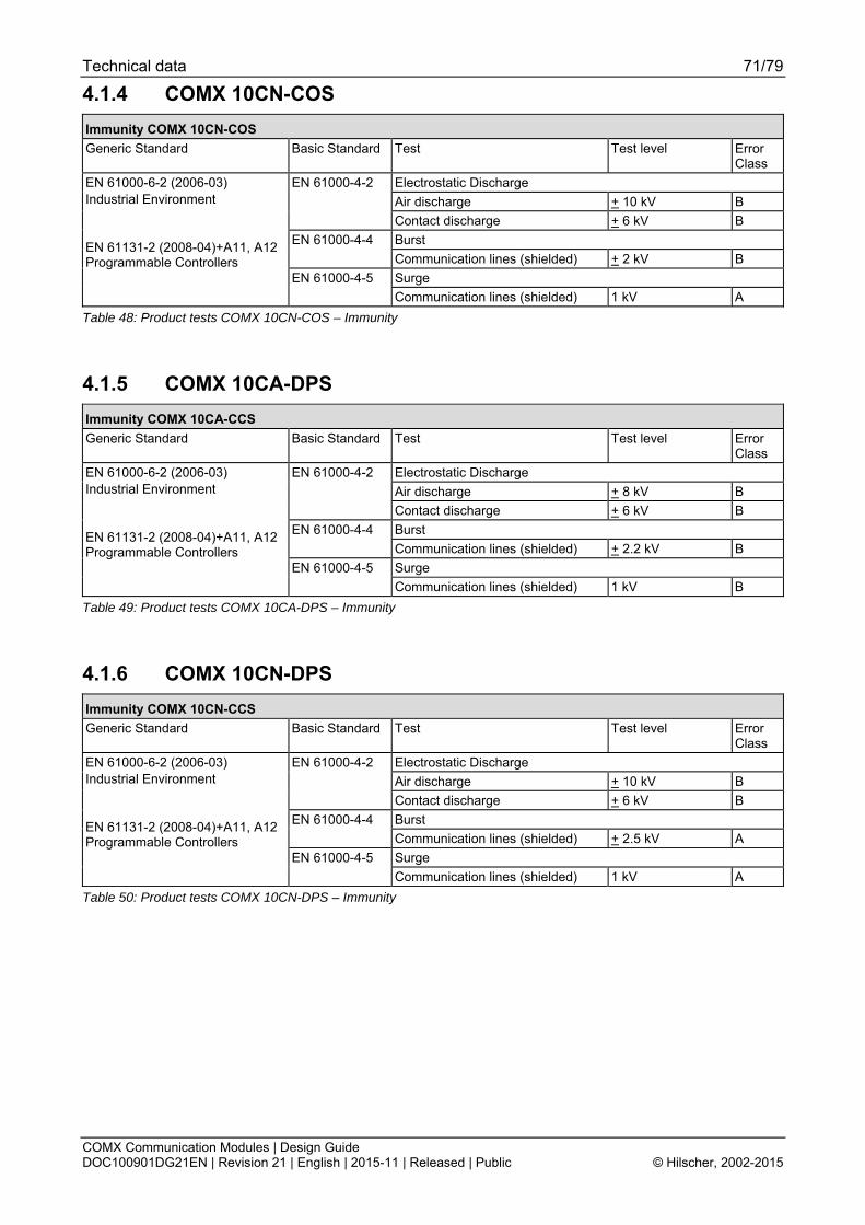
Technical data 71/79
COMX Communication Modules | Design Guide DOC100901DG21EN | Revision 21 | English | 2015-11 | Released | Public © Hilscher, 2002-2015
4.1.4 COMX 10CN-COS Immunity COMX 10CN-COS Generic Standard Basic Standard Test Test level Error
Class Electrostatic Discharge Air discharge + 10 kV B
EN 61000-4-2
Contact discharge + 6 kV B Burst EN 61000-4-4 Communication lines (shielded) + 2 kV B Surge
EN 61000-6-2 (2006-03) Industrial Environment EN 61131-2 (2008-04)+A11, A12 Programmable Controllers
EN 61000-4-5 Communication lines (shielded) 1 kV A
Table 48: Product tests COMX 10CN-COS – Immunity
4.1.5 COMX 10CA-DPS Immunity COMX 10CA-CCS Generic Standard Basic Standard Test Test level Error
Class Electrostatic Discharge Air discharge + 8 kV B
EN 61000-4-2
Contact discharge + 6 kV B Burst EN 61000-4-4 Communication lines (shielded) + 2.2 kV B Surge
EN 61000-6-2 (2006-03) Industrial Environment EN 61131-2 (2008-04)+A11, A12 Programmable Controllers
EN 61000-4-5 Communication lines (shielded) 1 kV B
Table 49: Product tests COMX 10CA-DPS – Immunity
4.1.6 COMX 10CN-DPS Immunity COMX 10CN-CCS Generic Standard Basic Standard Test Test level Error
Class Electrostatic Discharge Air discharge + 10 kV B
EN 61000-4-2
Contact discharge + 6 kV B Burst EN 61000-4-4 Communication lines (shielded) + 2.5 kV A Surge
EN 61000-6-2 (2006-03) Industrial Environment EN 61131-2 (2008-04)+A11, A12 Programmable Controllers
EN 61000-4-5 Communication lines (shielded) 1 kV A
Table 50: Product tests COMX 10CN-DPS – Immunity
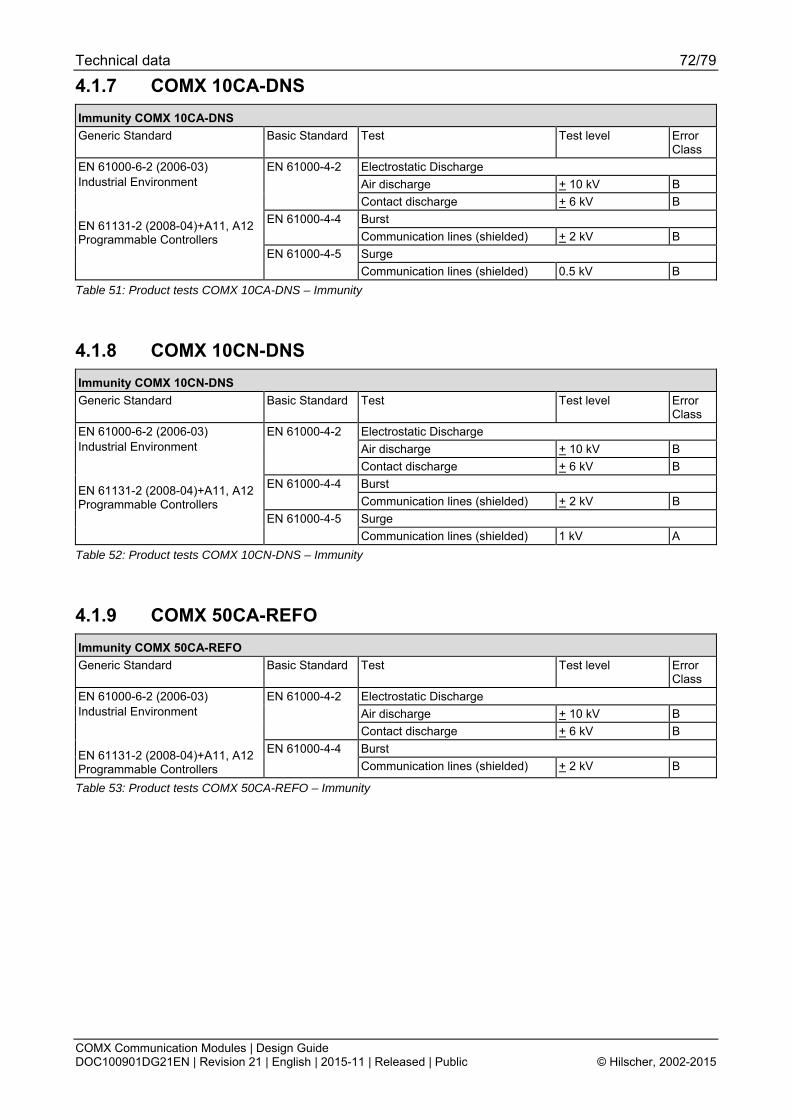
Technical data 72/79
COMX Communication Modules | Design Guide DOC100901DG21EN | Revision 21 | English | 2015-11 | Released | Public © Hilscher, 2002-2015
4.1.7 COMX 10CA-DNS Immunity COMX 10CA-DNS Generic Standard Basic Standard Test Test level Error
Class Electrostatic Discharge Air discharge + 10 kV B
EN 61000-4-2
Contact discharge + 6 kV B Burst EN 61000-4-4 Communication lines (shielded) + 2 kV B Surge
EN 61000-6-2 (2006-03) Industrial Environment EN 61131-2 (2008-04)+A11, A12 Programmable Controllers
EN 61000-4-5 Communication lines (shielded) 0.5 kV B
Table 51: Product tests COMX 10CA-DNS – Immunity
4.1.8 COMX 10CN-DNS Immunity COMX 10CN-DNS Generic Standard Basic Standard Test Test level Error
Class Electrostatic Discharge Air discharge + 10 kV B
EN 61000-4-2
Contact discharge + 6 kV B Burst EN 61000-4-4 Communication lines (shielded) + 2 kV B Surge
EN 61000-6-2 (2006-03) Industrial Environment EN 61131-2 (2008-04)+A11, A12 Programmable Controllers
EN 61000-4-5 Communication lines (shielded) 1 kV A
Table 52: Product tests COMX 10CN-DNS – Immunity
4.1.9 COMX 50CA-REFO Immunity COMX 50CA-REFO Generic Standard Basic Standard Test Test level Error
Class Electrostatic Discharge Air discharge + 10 kV B
EN 61000-4-2
Contact discharge + 6 kV B Burst
EN 61000-6-2 (2006-03) Industrial Environment EN 61131-2 (2008-04)+A11, A12 Programmable Controllers
EN 61000-4-4 Communication lines (shielded) + 2 kV B
Table 53: Product tests COMX 50CA-REFO – Immunity

Technical data 73/79
COMX Communication Modules | Design Guide DOC100901DG21EN | Revision 21 | English | 2015-11 | Released | Public © Hilscher, 2002-2015
4.1.10 COMX 50CA-CCS Immunity COMX 50CA-CCS Generic Standard Basic Standard Test Test level Error
Class Electrostatic Discharge Air discharge + 8 kV B
EN 61000-4-2
Contact discharge + 4 kV A Burst EN 61000-4-4 Communication lines (shielded) + 2 kV
fr = 5 kHz B
Surge
EN 61000-6-2 (2006-03) Industrial Environment EN 61131-2 (2008-04)+A11, A12 Programmable Controllers
EN 61000-4-5 Communication lines (shielded) 1 kV
2 Ohm / 18 μF A
Table 54: Product tests COMX 50CA-CCS – Immunity
4.1.11 COMX 51CA-RE Immunity COMX 51CA-RE Generic Standard Basic Standard Test Test level Error
Class Electrostatic Discharge Air discharge + 8 kV A
EN 61000-4-2
Contact discharge + 6 kV B Burst EN 61000-4-4 Communication lines (shielded) + 2.2 kV
fr = 5 kHz B
Surge
EN 61000-6-2 (2006-03) Industrial Environment EN 61131-2 (2008-04)+A11, A12 Programmable Controllers
EN 61000-4-5 Communication lines (shielded) 1 kV A
Table 55: Product tests COMX 51CA-RE – Immunity
4.1.12 COMX 51CN-RE Immunity COMX 51CN-RE Generic Standard Basic Standard Test Test level Error
Class Electrostatic Discharge Air discharge + 8 kV A
EN 61000-4-2
Contact discharge + 6 kV A Burst EN 61000-4-4 Communication lines (shielded) + 2.2 kV
fr = 5 kHz B
Surge
EN 61000-6-2 (2006-03) Industrial Environment EN 61131-2 (2008-04)+A11, A12 Programmable Controllers
EN 61000-4-5 Communication lines (shielded) 1 kV A
Table 56: Product tests COMX 51CN-RE – Immunity
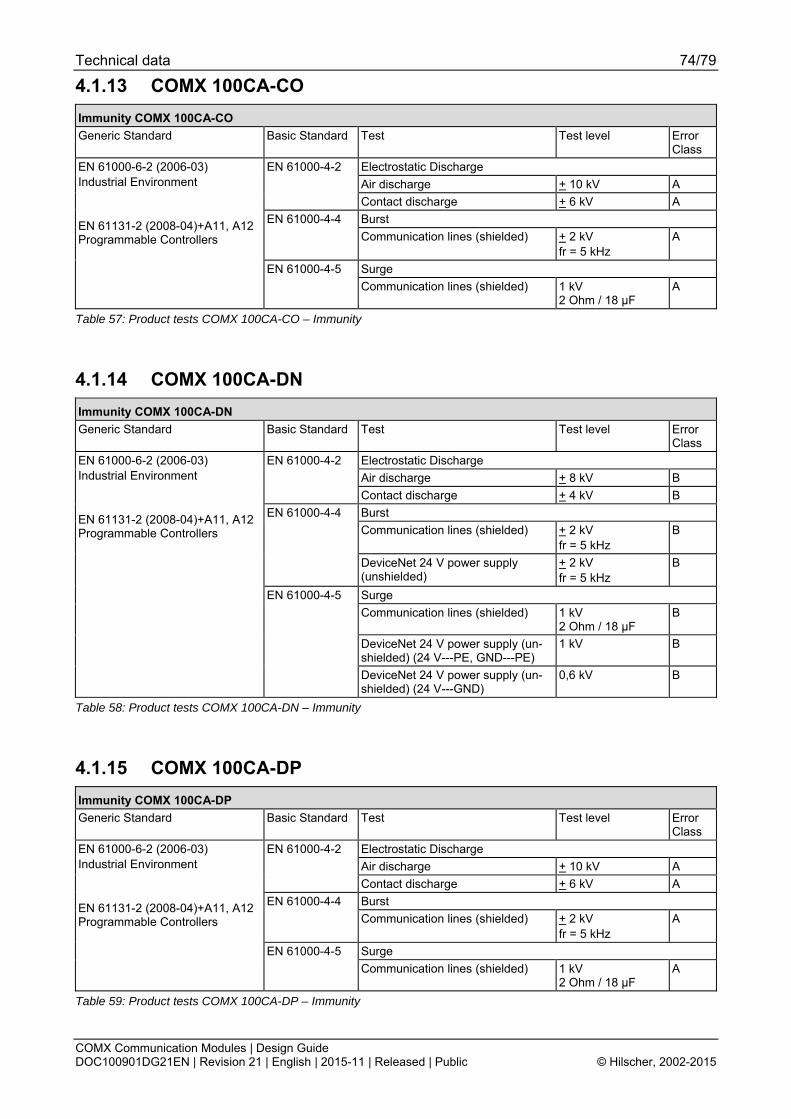
Technical data 74/79
COMX Communication Modules | Design Guide DOC100901DG21EN | Revision 21 | English | 2015-11 | Released | Public © Hilscher, 2002-2015
4.1.13 COMX 100CA-CO Immunity COMX 100CA-CO Generic Standard Basic Standard Test Test level Error
Class Electrostatic Discharge Air discharge + 10 kV A
EN 61000-4-2
Contact discharge + 6 kV A Burst EN 61000-4-4 Communication lines (shielded) + 2 kV
fr = 5 kHz A
Surge
EN 61000-6-2 (2006-03) Industrial Environment EN 61131-2 (2008-04)+A11, A12 Programmable Controllers
EN 61000-4-5 Communication lines (shielded) 1 kV
2 Ohm / 18 μF A
Table 57: Product tests COMX 100CA-CO – Immunity
4.1.14 COMX 100CA-DN Immunity COMX 100CA-DN Generic Standard Basic Standard Test Test level Error
Class Electrostatic Discharge Air discharge + 8 kV B
EN 61000-4-2
Contact discharge + 4 kV B Burst Communication lines (shielded) + 2 kV
fr = 5 kHz B
EN 61000-4-4
DeviceNet 24 V power supply (unshielded)
+ 2 kV fr = 5 kHz
B
Surge Communication lines (shielded) 1 kV
2 Ohm / 18 μF B
DeviceNet 24 V power supply (un-shielded) (24 V---PE, GND---PE)
1 kV B
EN 61000-6-2 (2006-03) Industrial Environment EN 61131-2 (2008-04)+A11, A12 Programmable Controllers
EN 61000-4-5
DeviceNet 24 V power supply (un-shielded) (24 V---GND)
0,6 kV B
Table 58: Product tests COMX 100CA-DN – Immunity
4.1.15 COMX 100CA-DP Immunity COMX 100CA-DP Generic Standard Basic Standard Test Test level Error
Class Electrostatic Discharge Air discharge + 10 kV A
EN 61000-4-2
Contact discharge + 6 kV A Burst EN 61000-4-4 Communication lines (shielded) + 2 kV
fr = 5 kHz A
Surge
EN 61000-6-2 (2006-03) Industrial Environment EN 61131-2 (2008-04)+A11, A12 Programmable Controllers
EN 61000-4-5 Communication lines (shielded) 1 kV
2 Ohm / 18 μF A
Table 59: Product tests COMX 100CA-DP – Immunity

Technical data 75/79
COMX Communication Modules | Design Guide DOC100901DG21EN | Revision 21 | English | 2015-11 | Released | Public © Hilscher, 2002-2015
4.1.16 COMX 100CA-RE Immunity COMX 100CA-RE Rev.8 Generic Standard Basic Standard Test Test level Error
Class Electrostatic Discharge EN 61000-4-2 Contact discharge + 6 kV B Burst EN 61000-4-4 Communication lines (shielded) + 2 kV
fr = 5 kHz B
Surge
EN 61000-6-2 (2006-03) Industrial Environment EN 61131-2 (2008-04)+A11, A12 Programmable Controllers
EN 61000-4-5 Communication lines (shielded) 1 kV A
Table 60: Product tests COMX 100CA-RE Rev.8 – Immunity
4.1.17 COMX 100CN-CO Immunity COMX 100CN-CO Generic Standard Basic Standard Test Test level Error
Class Electrostatic Discharge Air discharge + 10 kV B
EN 61000-4-2
Contact discharge + 6 kV B Burst EN 61000-4-4 Communication lines + 2 kV
fr = 5 kHz A
Surge
EN 61000-6-2 (2006-03) Industrial Environment EN 61131-2 (2008-04)+A11, A12 Programmable Controllers
EN 61000-4-5 Communication lines (shielded) 1 kV
2 Ohm / 18 μF A
Table 61: Product tests COMX 100CN-CO – Immunity
4.1.18 COMX 100CN-DN Immunity COMX 100CN-DN Generic Standard Basic Standard Test Test level Error
Class Electrostatic Discharge Air discharge + 10 kV B
EN 61000-4-2
Contact discharge + 6 kV B Burst Communication lines (shielded) + 2 kV
fr = 5 kHz B
EN 61000-4-4
DeviceNet 24 V power supply (unshielded)
+ 2 kV fr = 5 kHz
B
Surge Communication lines (shielded) 1 kV
2 Ohm / 18 μF B
DeviceNet 24 V power supply (unshielded) (24 V---PE, GND---PE)
1 kV B
EN 61000-6-2 (2006-03) Industrial Environment EN 61131-2 (2008-04)+A11, A12 Programmable Controllers
EN 61000-4-5
DeviceNet 24 V power supply (unshielded) (24 V---GND)
0,6 kV B
Table 62: Product tests COMX 100CN-DN – Immunity
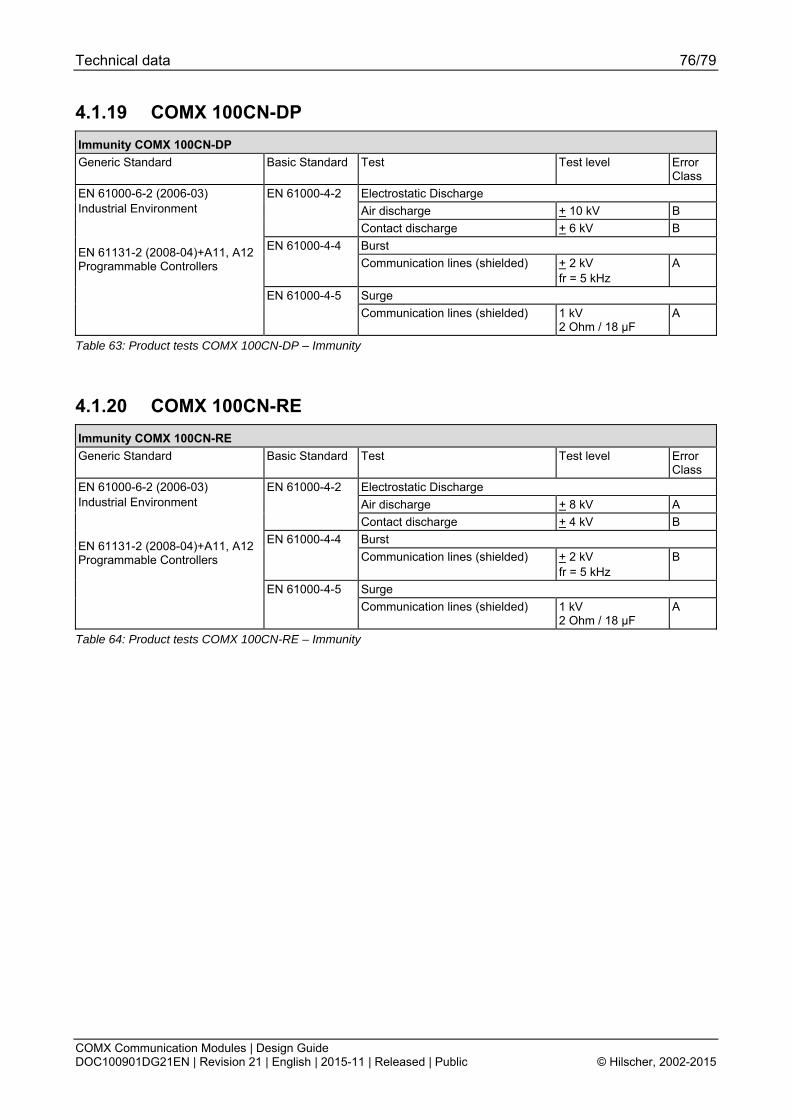
Technical data 76/79
COMX Communication Modules | Design Guide DOC100901DG21EN | Revision 21 | English | 2015-11 | Released | Public © Hilscher, 2002-2015
4.1.19 COMX 100CN-DP Immunity COMX 100CN-DP Generic Standard Basic Standard Test Test level Error
Class Electrostatic Discharge Air discharge + 10 kV B
EN 61000-4-2
Contact discharge + 6 kV B Burst EN 61000-4-4 Communication lines (shielded) + 2 kV
fr = 5 kHz A
Surge
EN 61000-6-2 (2006-03) Industrial Environment EN 61131-2 (2008-04)+A11, A12 Programmable Controllers
EN 61000-4-5 Communication lines (shielded) 1 kV
2 Ohm / 18 μF A
Table 63: Product tests COMX 100CN-DP – Immunity
4.1.20 COMX 100CN-RE Immunity COMX 100CN-RE Generic Standard Basic Standard Test Test level Error
Class Electrostatic Discharge Air discharge + 8 kV A
EN 61000-4-2
Contact discharge + 4 kV B Burst EN 61000-4-4 Communication lines (shielded) + 2 kV
fr = 5 kHz B
Surge
EN 61000-6-2 (2006-03) Industrial Environment EN 61131-2 (2008-04)+A11, A12 Programmable Controllers
EN 61000-4-5 Communication lines (shielded) 1 kV
2 Ohm / 18 μF A
Table 64: Product tests COMX 100CN-RE – Immunity
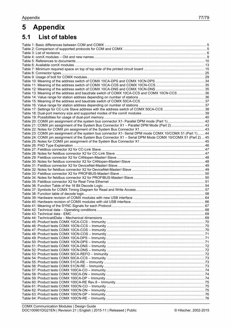
Appendix 77/79
COMX Communication Modules | Design Guide DOC100901DG21EN | Revision 21 | English | 2015-11 | Released | Public © Hilscher, 2002-2015
5 Appendix 5.1 List of tables Table 1: Basic differences between COM and COMX ........................................................................................................ 5 Table 2: Comparison of supported protocols for COM and COMX ..................................................................................... 5 Table 3: List of revisions ..................................................................................................................................................... 6 Table 4: comX modules Old and new names................................................................................................................... 9 Table 5: References to documents ................................................................................................................................... 10 Table 6: Available comX modules ..................................................................................................................................... 13 Table 7: Minimum required space on top of top side of the printed circuit board .............................................................. 15 Table 8: Connector types .................................................................................................................................................. 25 Table 9: Usage of bolt for COMX modules........................................................................................................................ 29 Table 10: Meaning of the address switch of COMX 10CA-DPS and COMX 10CN-DPS .................................................. 34 Table 11: Meaning of the address switch of COMX 10CA-COS and COMX 10CN-CCS.................................................. 35 Table 12: Meaning of the address switch of COMX 10CA-DNS and COMX 10CN-DNS .................................................. 35 Table 13: Meaning of the address and baudrate switch of COMX 10CA-CCS and COMX 10CN-CCS ............................ 36 Table 14: Value range for station address depending on number of stations ................................................................... 36 Table 15: Meaning of the address and baudrate switch of COMX 50CA-CCS.................................................................. 37 Table 16: Value range for station address depending on number of stations ................................................................... 37 Table 17: Settings for CC-Link Slave address with the address switch of COMX 50CA-CCS .......................................... 38 Table 18: Dual-port memory size and supported modes of the comX modules ................................................................ 39 Table 19: Possibilities for usage of dual-port memory....................................................................................................... 40 Table 20: COMX pin assignment of the system bus connector X1- Parallel DPM mode (Part 1)...................................... 42 Table 21: COMX pin assignment of the System Bus Connector X1 Parallel DPM Mode (Part 2) .................................. 43 Table 22: Notes for COMX pin assignment of the System Bus Connector X1 .................................................................. 43 Table 23: COMX pin assignment of the system bus connector X1- Serial DPM mode COMX 10/COMX 51 (Part 1) ....... 44 Table 24: COMX pin assignment of the System Bus Connector X1 Serial DPM Mode COMX 10/COMX 51 (Part 2) ... 45 Table 25: Notes for COMX pin assignment of the System Bus Connector X1 .................................................................. 45 Table 26: PAD Type Explanation ...................................................................................................................................... 46 Table 27: Fieldbus connector X2 for CC-Link Slave.......................................................................................................... 47 Table 28: Notes for fieldbus connector X2 for CC-Link Slave ........................................................................................... 47 Table 29: Fieldbus connector X2 for CANopen-Master/-Slave.......................................................................................... 48 Table 30: Notes for fieldbus connector X2 for CANopen-Master/-Slave ........................................................................... 48 Table 31: Fieldbus connector X2 for DeviceNet-Master/-Slave......................................................................................... 49 Table 32: Notes for fieldbus connector X2 for DeviceNet-Master/-Slave .......................................................................... 49 Table 33: Fieldbus connector X2 for PROFIBUS-Master/-Slave ....................................................................................... 50 Table 34: Notes for fieldbus connector X2 for PROFIBUS-Master/-Slave......................................................................... 50 Table 35: Fieldbus connector X2 for Real-Time Ethernet ................................................................................................. 51 Table 36: Function Table of the 16 Bit Decode Logic........................................................................................................ 54 Table 37: Symbols for COMX Timing Diagram for Read and Write Access...................................................................... 57 Table 38: Function table of decode logic........................................................................................................................... 58 Table 39: Hardware revision of COMX modules with new USB interface ......................................................................... 64 Table 40: Hardware revision of COMX modules with old USB interface ........................................................................... 66 Table 41: Meaning of the SYNC Signals for each Protocol ............................................................................................... 67 Table 42: Technical data Operating conditions .............................................................................................................. 68 Table 43: Technical data - EMC........................................................................................................................................ 69 Table 44: TechnicaldData Mechanical dimensions ........................................................................................................ 69 Table 45: Product tests COMX 10CA-CCS Immunity .................................................................................................... 70 Table 46: Product tests COMX 10CN-CCS Immunity .................................................................................................... 70 Table 47: Product tests COMX 10CA-COS Immunity .................................................................................................... 70 Table 48: Product tests COMX 10CN-COS Immunity .................................................................................................... 71 Table 49: Product tests COMX 10CA-DPS Immunity..................................................................................................... 71 Table 50: Product tests COMX 10CN-DPS Immunity .................................................................................................... 71 Table 51: Product tests COMX 10CA-DNS Immunity .................................................................................................... 72 Table 52: Product tests COMX 10CN-DNS Immunity .................................................................................................... 72 Table 53: Product tests COMX 50CA-REFO Immunity .................................................................................................. 72 Table 54: Product tests COMX 50CA-CCS Immunity .................................................................................................... 73 Table 55: Product tests COMX 51CA-RE Immunity ....................................................................................................... 73 Table 56: Product tests COMX 51CN-RE Immunity....................................................................................................... 73 Table 57: Product tests COMX 100CA-CO Immunity..................................................................................................... 74 Table 58: Product tests COMX 100CA-DN Immunity..................................................................................................... 74 Table 59: Product tests COMX 100CA-DP Immunity ..................................................................................................... 74 Table 60: Product tests COMX 100CA-RE Rev.8 Immunity........................................................................................... 75 Table 61: Product tests COMX 100CN-CO Immunity .................................................................................................... 75 Table 62: Product tests COMX 100CN-DN Immunity..................................................................................................... 75 Table 63: Product tests COMX 100CN-DP Immunity..................................................................................................... 76 Table 64: Product tests COMX 100CN-RE Immunity..................................................................................................... 76
Appendix 78/79
COMX Communication Modules | Design Guide DOC100901DG21EN | Revision 21 | English | 2015-11 | Released | Public © Hilscher, 2002-2015
5.2 List of figures Figure 1: Block diagram of the COMX modules .................................................................................................................. 8 Figure 2: COMX CA type - Connector X1.......................................................................................................................... 14 Figure 3: COMX CN type - Connectors X1 and X2 ........................................................................................................... 14 Figure 4: How to layout the signals at the connectors X1 and X2 ..................................................................................... 28 Figure 5: Example matrix code label of COMX modules................................................................................................... 34 Figure 6: Schematic view of netX pad types ..................................................................................................................... 46 Figure 7: Ethernet connection COMX-CN-RE................................................................................................................... 52 Figure 8: Ethernet connector example (ERNI 203313) ..................................................................................................... 52 Figure 9: COMX timing diagram for read access .............................................................................................................. 56 Figure 10: COMX timing diagram for write access ............................................................................................................ 56 Figure 11: Interface with 8-bit data bus - Interface with 16-bit interface ............................................................................ 58 Figure 12: Serial dual-port memory interface .................................................................................................................... 59 Figure 13: Fieldbus interface connections......................................................................................................................... 60 Figure 14: Example how to connect the LEDs COMX CN fieldbus ................................................................................... 61 Figure 15: Example how to connect the LEDs COMX CN-RE .......................................................................................... 62 Figure 16: RS232C interface circuit for the diagnostic interface........................................................................................ 63 Figure 17: USB interface circuit for the diagnostic interface.............................................................................................. 64 Figure 18: USB interface circuit modification for the diagnostic interface.......................................................................... 65

Appendix 79/79
COMX Communication Modules | Design Guide DOC100901DG21EN | Revision 21 | English | 2015-11 | Released | Public © Hilscher, 2002-2015
5.3 Contacts
Headquarters Germany Hilscher Gesellschaft für Systemautomation mbH Rheinstrasse 15 65795 Hattersheim Phone: +49 (0) 6190 9907-0 Fax: +49 (0) 6190 9907-50 E-Mail: [email protected] Support Phone: +49 (0) 6190 9907-99 E-Mail: [email protected]
Subsidiaries
China Hilscher Systemautomation (Shanghai) Co. Ltd. 200010 Shanghai Phone: +86 (0) 21-6355-5161 E-Mail: [email protected] Support Phone: +86 (0) 21-6355-5161 E-Mail: [email protected] France Hilscher France S.a.r.l. 69500 Bron Phone: +33 (0) 4 72 37 98 40 E-Mail: [email protected] Support Phone: +33 (0) 4 72 37 98 40 E-Mail: [email protected] India Hilscher India Pvt. Ltd. Pune, Delhi, Mumbai Phone: +91 8888 750 777 E-Mail: [email protected] Italy Hilscher Italia S.r.l. 20090 Vimodrone (MI) Phone: +39 02 25007068 E-Mail: [email protected] Support Phone: +39 02 25007068 E-Mail: [email protected]
Japan Hilscher Japan KK Tokyo, 160-0022 Phone: +81 (0) 3-5362-0521 E-Mail: [email protected] Support Phone: +81 (0) 3-5362-0521 E-Mail: [email protected] Korea Hilscher Korea Inc. Seongnam, Gyeonggi, 463-400 Phone: +82 (0) 31-789-3715 E-Mail: [email protected] Switzerland Hilscher Swiss GmbH 4500 Solothurn Phone: +41 (0) 32 623 6633 E-Mail: [email protected] Support Phone: +49 (0) 6190 9907-99 E-Mail: [email protected] USA Hilscher North America, Inc. Lisle, IL 60532 Phone: +1 630-505-5301 E-Mail: [email protected] Support Phone: +1 630-505-5301 E-Mail: [email protected]