composition, structure, and hardness of pulse plated ...infohouse.p2ric.org/ref/28/27291.pdf ·...
TRANSCRIPT

COMPOSITION, STRUCTURE, AND HARDNESS OF PULSE PLATED NICKEL-HARDENED GOLD FILMS
G. Holmbom Industrial Microelectronics Centre, Linkoping University/lFM, S-581 83 Linkoping, Sweden
B. E. Jacobson CN-Europe, Orangenet, S-612 01 Finspong, Sweden
J.-E. Sundgren Dept of Physics and Measurement Techn., Linkoping Institute of Technology, S-581 83 Linkoping, Sweden
ABSTRACT
Composition, microstructure, and hardness are essential for the wear characteristics of electroplated hard gold films in sliding contact applications. Pulse plating has proved to be a useful deposition technique with process characteristics allowing good control over both alloy composition and microstructure. In this study, Ni-alloyed Au films were prepared by electroplating using both DC and pulsed current deposition. It was found that the Ni content (< 2.5 at%) increases with a decrease of the average current density and with decreasing pulse duration. All deposits had average grain sizes ranging from 16 to 28 nm and contained numerous non-crystalline inclusions about 2 nm in diameter with average spacing from 12 to 30 nm. The hardness values of the fine grained films were ranging from VHN,, = 200 to 225 while the hardness of the coarse grained films was less than VHN,, = 170. The study shows that the increased hardness of alloyed gold films is dominated by a grain size refinement rather than dispersion hardening due to particle distributions or solid solution strengthening.
INTRODUCTION
Alloyed gold, so called hard gold, is the most commonly used material for sliding contacts in electronics industry. The most commonly used alloying elements are Co and Ni which are added in concentrations of less than 3 at% (1 wt%). Other alloying elements are e.g. arsenic. Pure electrodeposited gold is soft with a Vickers Hardness Number of about VHN = 80 and has a high wear rate particularly in situations where abrasive wear is dominant, while the alloyed gold is significantly harder, above VHN = 200,
and exhibits improved wear properties. There are three possible hardening mechanisms which can contribute to the hardness of the alloyed Au films: solid solution hardening due to Ni or Co atoms substitutionally dissolved in the Au lattice, grain size hardening due to reduced grain size, and dispersion hardening due to inclusions dispersed in the Au matrix. Lo et al.’ concluded that for Co-hardened gold, grain size effects dominate. However, earlier studies2 have shown contradictory results. It is a fact that when DC plating is applied, the alloy content, grain size and inclusion density are difficult to separate while pulse plating makes it possible to vary the three parameters at a fixed average current density. In this way it is possible to separate the effect of each hardening mechanism.
By pulse plating, the current characteristics can be used to control the composition of the films. Models based on mass transport of the alloy species in the vicinity of the cathode have Feen developed by Tannenterger and Schindler and by Dossenbach et al. for the Pd-Ni and Ag-Pd systems, respectively. Those models are based on the fact that the more noble metal is initially deposited at the applied current density until it becomes mass transport limited. The partial current density for the noble metal then drops to the limiting current density and the less noble metal starts to deposit. By varying the pulse duration the composition can be altered in a
and hydrodynamical conditions are known and brought under control.
The alloyed gold does not only contain codeposited Ni or Co but also significant quantities of carbon, nitrogen, hydrogen,
controlled way provided that the electrochemical ~~~
1
333
oxygen, and potassium6-'. A large fraction of those elements is in the form of inclusions in the
. They have a t ical size microstructure distribution in the range of 1 to 5 nmy82. These inclusions can affect the microstructure and the hardness of gold. They can have a grain refining effect3 and also contribute to the hardness through dispersion hardeningg. In the case of Co-alloyed Au and pure sputtered Au films studied by Lo et al.' it was concluded that the hardness is improved by grain size reduction. For Ni-alloyed Au, however, there is no literature data.
In this work, spdies were made on the effect of pulse plating on composition, microstructure, and micro-hardness of Ni-alloyed Au. The mass transfer based model introduced by Tannen- berger proved to be valid also for the Au-Ni system, at least qualitatively. The micro- hardness of the deposits was measured and correlated to the alloy content and micro- structure. The relative influence of possible hardening mechanisms were evaluated. It is shown that the grain size reduction is the dominant hardening mechanism in Ni-alloyed gold films.
2 8 9-12
EXPERIMENTAL
Gold was deposited from a citrate buffered bath with 10 g/l Au (added as KAu(CN)2), 0.6 g/l Ni (added as Ni-citrate), and 150 g/l citric acid. The bath was operated at 40°C and pH 3.9 (adjusted by addition of KOH). The deposition was carried out in a flow channel with non-turbulent electrolyte flow passing the electrodes. The gold was deposited onto standard printed circuit board Cu substrates (3 x 8.3 = 25 cm2 in size).
The Cu substrates exhibited a columnar structure with an average column diameter of 3 pm. Prior to deposition they were cleaned for one minute by anodic electrolytic degreasing in a metasilicate alkaline solution for one minute at room temperature and a current density of 20 mA/cm2. To obtain a smoothness which would not affect the topography of the film the cleaning was followed by electropolishing for one minute in a mixture of 775 ml/l orthophosphoric acid and 225 ml/l propylene glycol at room temperature and a current density of 350 mNcr2 . The substrates were activated for 30 seconds in 20% sulphuric acid at room temperature immediately prior to gold deposition.
The thickness of the Au-Ni films was 2 pm for composition measurements and structure analyses and 20 pm for hardness measurements. The current was rectangular cathodic pulsating at two average current densities, 5 mA/cmz and 10 mA/cm2, and three duty cycles, 50%, 20%, and 5%. At each average current density and duty cycle samples were prepared at four relaxation times 900 ms, 50 ms, 5 ms, and 0.5 ms. Reference samples were also prepared by DC plating at 5 and 10 mA/cm2.
For comparison, Au-Ni films were prepared by electron beam co-evaporation from two sources to form alloys over a wide range of concentrations. The films were prepared at a pressure of less than 5 ~ 1 O - ~ Pa and deposited onto glass substrates held at 300°C. The total deposition rate varied between 0.5 and 0.75 pm/min and the final film thickness between 2 and 3.5 pm. The experimental equipment used for these experiments is described in detail in reference 13.
The chemical composition of the electroplated films was measured by atomic absorption spectroscopy. The Cu substrates were dissolved in 25% HNO3 and the films were subsequently dissolved in aqua regia (no Ni was detected in the HNO3 residue by atomic absorption). The composition of evaporated films was measured by X-ray energy dispersive spectroscopy (EDS) using a ZAF correction program (LINK ZAF4). The structure analyses were performed by transmission electron microscopy (TEM) using a Philips EM400T operated at 100 and 120 kV. The TEM samples were prepared as 3 mm discs using a hollow diamond-tipped drill. The Cu substrates were dissolved in 25% HNO3, leaving a 2 pm thick Au-Ni disc which was finally thinned to electron transparency by Ar+- ion beam milling at 3 kV, 0.4 mA emission current, and a 13" angle of incidence. The samples were cooled with liquid nitrogen to avoid heating and radiation damage. The grain size measurements were given as an average value of more than 100 grains. The interparticle spacings were measured by counting 100 to 200 inclusions in a volume of a film with an estimated thickness of 100 nm.
The micro-hardness of the films was measured in an optical microscope equipped with a Vickers diamond shaped indentor. These measurements were carried out at a load of 1 N and with 10 indents on each sample. The load
.
-
2
334

.
Load Hardness
("1 (VHN)
50 215 f 8
100 220 f 11
200 199 k 8
400 221 f 3
600 227 f 5
800 222 f 9
1000 226 f 8 L
RESULTS AND DISCUSSION
Composition of Au-Ni alloys.- For DC deposition the composition of the Au-Ni alloys, for a given bath composition and constant hydrodynamic conditions, depends on the current density while for pulse plating it depends on both the average current density (Jave) and the pulse shape and duration. The NI content increases with decreased Jave both for DC and pulse plating.
When the pulse duration (Td, is changed, the composition of the Au-Ni films is altered as illustrated in Fig. 1. For Jc = 5 mA/cm2, the Ni content is approximately 1.0 at% when long pulse durations (Tc = 47 to 900 ms) are used. For shorter Tc values, the Ni content first increases and reaches a maximum for Tc = 0.1 to 5 ms and then decreases to a level slightly above that obtained ior long plating cycles, i.e. 1.3 to 1.6 at%. This is equal to the Ni content of DC deposits, 1.5 at%. At higher average current density, 10 mA/cmz, similar tendencies are observed as Tc is altered although the absolute
Ni concentrations are lower as shown in Fig. 1. Both for Jave = 5 and 10 mA/cm2 the obtained maximum in the Ni content is shifted to longer pulse durations as the duty cycles increases.
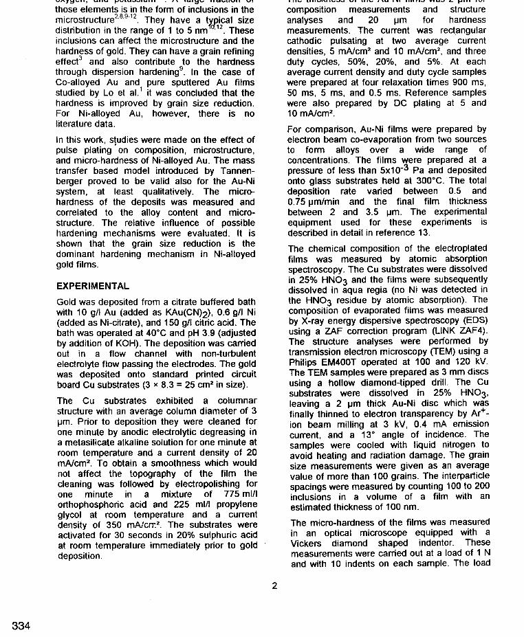
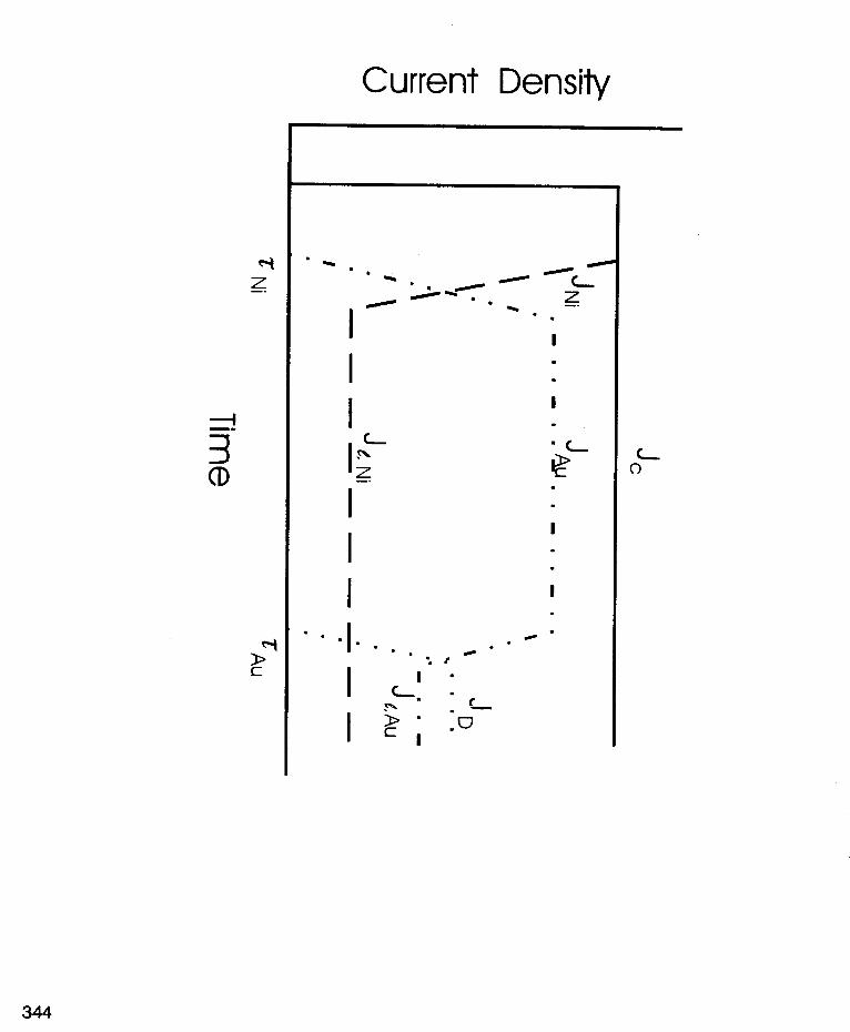
In the Au-Ni system Ni deposits at more positive potentials than Au'~. This explains why the Ni- content increases at decreased Jave. The electrochemical potentials are important for the sequence in which the metals are deposited as illustrated in Fig. 24,5. The more noble species, Ni, is deposited at the applied current density (J,-.J until it becomes mass transport limited at the transition time TNi. Fort >TNi Ni is deposited at the diffusion limited current density (Jt,Ni). As JNi starts to decrease at TNi the less noble species, Au, start to deposit and J A ~ will approach Jc - Jt,Ni at which Au is deposited until it becomes mass transport limited at time T A ~ . The composition of the alloy can thus be controlled by choosing Tc in the range of TNi < Tc < TNi + TAU. If Tc is longer than TNi + TA,,
the composition will be determined by the ratio Jt,Ni to Jt,Au. When applying the model described in reference 4 to the Au-Ni system it has to be slightly modified due to the different valence numbers of Au+ and Ni2+. The amount of deposited material at time t for TNi < t < TNi + T A ~ expressed in molar quantities is
where n is the valence number and F the faraday constant. The Ni content can thus be calculated as
This model was developed for well controlled conditions with long relaxation time (Teff) - a necessary condition for accurate alloy content calculation. Under production-like conditions, i.e. higher average current densities and frequencies, the electrochemical properties are not so easily defined. Furthermore, in the Au-Ni system the current efficiency is of the order of 20 to 35% which makes the interpretation even more complicated. However, in spite of these difficulties the model can still be used as a tool
3
335

to predict and to interpret the variations in alloy composition due to varying pulse parameters.
By decreasing Tc and Teff at constant Jc, i.e. maintaining the duty cycle (Tc /[Tc + Teff]) constant while increasing the frequency, the fraction of each plating cycle where Ni is deposited at Jc is increased resulting in an increased Ni content in the deposits. However, at very short pulse cycles the relaxation time will be so short that only a small amount of Ni has time to diffuse back into the diffusion layer. This causes TNi to decrease. According to lb115 ZNi can be calculated as follows:
sc T ~ , J : = -DN,(nFcNi)' 4 [41
where DNi is the diffusion coefficient of Ni ions and CNi the concentration of Ni. Under very slow pulsating conditions and at low Jave the bulk concentration of Ni can be used in equation [4]. However, when both the frequency and the average current density are increased the Ni concentration at the electrode surface differs from the bulk value. The surface concentration at the beginning of a pulse can be calculated
as foltows: r T J
(6,-6,) [51 ' c c, = c,, --
nFD (Tc + T,,")
where co is the bulk concentration and 8~ and Fp the thicknesses of the static and pulsating diffusion layers, re~pectively'~. When the duty cycle and Jc is constant only tip varies with Tc, i.e. Ce decreases with decreasing Tc. This results in a reduction of z according to equation [4]. Consequently, an even smaller fraction of Ni can be deposited at Jc. As a result Au deposition is favoured and approaches the DC plating condition.
The maximum concentration of Ni is obtained at shorter T,'s when Jc is high (Fig. 1). According to equation [4], the transition time of Ni decreases as :i.~i)-% when Jc is increased and, consequently, the maximum Ni concentration is shifted towards shorter Tc. Furthermore, in the high-frequency region 'CNi is reduced due to the reduction in the surface concentration of Ni in the same way as described above.
To summarise the effect of pulse plating on alloy composition we would like to emphasise that pulse plating is an excellent way to tailor alloy omp position'^.^^ of electrodeposits. This will probably be one of the key future developments for high technology applications of electroplating.
~
~
-
2.5
2
1 5 .- z
m s +
1
0 5
0 0.01
Composition of AuNi Films
A
:
0.1 10 im 1mo h e Duration
(ms)
-50% d c 5 mNcm' - * - 2 O % d c 5 m N c " * 5 % d c 5mNcm'
-50% d c 10 mNcm' - 0 - 20% d C 10 mA/cm' --e- 5 % d c 10mA/cm*
DC5mNcm' 0 ~ 1 0 ° C "
Figure 1. Ni content as a function of pulse duration at average current densities of 5 and 10 mA/cm2 ant duty cycles of 50%, 25%, and 5%. Composition under DC conditions to the left.
4
336
Jc
\ I
1‘ \
\ JD . . . .
I
Ni ‘Au
Time Figure 2. Representation of partial current densities of a fwo-metal plating system under pulsed current conditions.
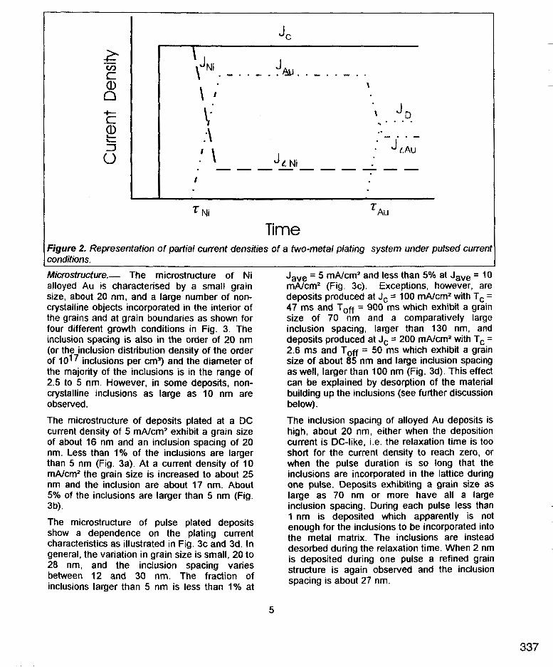
MiCrosfrur3ure.- The microstructure of Ni alloyed Au is characterised by a small grain size, about 20 nm, and a large number of non- crystalline objects incorporated in the interior of the grains and at grain boundaries as shown for four different growth conditions in Fig. 3. The inclusion spacing is also in the order of 20 nm (or the inclusion distribution density of the order of 1 O1 inclusions per cm3) and the diameter of the majority of the inclusions is in the range of 2.5 to 5 nm. However, in some deposits, non- crystalline inclusions as large as 10 nm are observed.
The microstructure of deposits plated at a DC current density of 5 mA/cm2 exhibit a grain size of about 16 nm and an inclusion spacing of 20 nm. Less than 1% of the inclusions are larger than 5 nm (Fig. 3a). At a current density of 10 mA/cm2 the grain size is increased to about 25 nm and the inclusion are about 17 nm. About 5% of the inclusions are larger than 5 nm (Fig. 3b).
The microstructure of pulse plated deposits show a dependence on the plating current characteristics as illustrated in Fig. 3c and 3d. In general, the variation in grain size is small, 20 to 28 nm, and the inclusion spacing vanes between 12 and 30 nm. The fraction of inclusions larger than 5 nm is less than 1% at
Jave = 5 mA/cm2 and less than 5% at Jave = 10 mA/cmz (Fig. 3c). Exceptions, however, are deposits produced at J, = 100 mA/cm2 with Tc = 47 ms and Teff = 900 ms which exhibit a grain size of 70 nm and a comparatively large inclusion spacing, larger than 130 nm, and deposits produced at Jc = 200 mNcm2 with Tc = 2.6 ms and Teff = 50 ms which exhibit a grain size of about 85 nm and large inclusion spacing as well, larger than 100 nm (Fig. 3d). This effect can be explained by desorption of the material building up the inclusions (see further discussion below).
The inclusion spacing of alloyed Au deposits is high, about 20 nm, either when the deposition current is DC-like, i.e. the relaxation time is too short for the current density to reach zero, or when the pulse duration is so long that the inclusions are incorporated in the lattice during one pulse. Deposits exhibiting a grain size as large as 70 nm or more have all a large inclusion spacing. During each pulse less than 1 nm is deposited which apparently is not enough for the inclusions to be incorporated into the metal matrix. The inclusions are instead desorbed during the relaxation time. When 2 nm is deposited during one pulse a refined grain structure is again observed and the inclusion spacing is about 27 nm.
5
337

Figure 3. Microstructure of electrodeposited Au-Ni alloys as revealed by TEM. In a) a DC plated film deposited at 5 mA/cm2. Average grain size 16 nm and inclusions (marked by the white arrows) about 3 nm in diameter and 20 nm average spacing. Less than 1% of the inclusions are larger than 5 nm. b) shows a DC plated film at 10 mA/cm*. Average grain size 26 nm and inclusion spacing about 17 nm. Approximately 5% of the inclusions are larger than 5 nm. c) shows a pulse plated deposit prepared at J, = 25 mNcm*, T, = 130 ps, and To# = 500 ps. Average grain size 25 nm and inclusion spacing 12 nm. d) shows a coarse grained deposit prepared by pulse plating at Jc = 100 mA/cm2, T, = 47 ms, and Teff = 900 ms is shown. Average grain size is 70 nm and inclusion spacing larger than 130 nm.
6
338

120
100
80
2 I > 60
40
20
0
Vickers hardness of PVD AuNi Films
. .
0 2 4 6 8 10 12 14
at% Ni
5gure 4. Vickers hardness (50 mN load) vs Ni content of Au-Ni films co-evaporated onto glass wbstrates held at Ts = 300'C. nclusions in Co and Ni hardened Au were
studied in d e p l by Okinaka and Nakahara" and Mausli et al. . The former could identify a size distribution of two major groups of inclusions about 2.5 and 5 nm in size, respectively, and an inclusion distribution density of the order 1017 ~ m - ~ , i.e. an inclusion spacing of about 20 nm. The latter found a distribution exhibiting smaller inclusions of 1.3 nm and a particle spacing of only 5 nm. Okinaka and Nakahara" concluded that the inclusions smaller than 5 nm consist of some specific polymeric species rather than entrapped gas and that they could act as sites for preferential nucleation thus preventing the characteristic growth of the pure gold deposit which normally would exhibit q;ain sizes at least one order of magnitude larger . It was also suggested" that the inclusions larger than 5 nm are gas filled and have less influence on the grain refinement. Conclusively, this work confirms the grain refining effect of the inclusions. Their presence reduces the mobility of adatoms on the growing surface and a fine
columnar structure is developed, which agrees with what has been reported by Nakaharalg.
To summarise the effect of pulse plating on microstructure we would like to point out the importance of desorption of non-metallic species and thus the enhanced purity of those deposits. In other applications, as e.g. Cr and Zn plating, hydrogen is evolved during the deposition and permeates into the metal. If appropriate process parameters are used it can be assumed that hydrogen can desorb during the relaxation time and thus reduce the problems with crack formation and hydrogen embrittlement.
Hardness of Au-Ni alloy deposits.- The hardness of electrodeposited Au-Ni alloys differs significantly from that of pure gold deposits. It is typically in the order of VHN = 200 and 80 for alloyed and pure gold, respectively. For comparison, the hardness of pure bulk Au is VHN - 50.
7
339
Vickers Hardness of AuNi Films
A
.
A A
A
A
A H
m
A
I
250
200
1 50
z 5
100
50
0 0 50 100 150 200 250 300 j.Loetal[l]
Grain Size (nm)””
/ ~ T h t s work
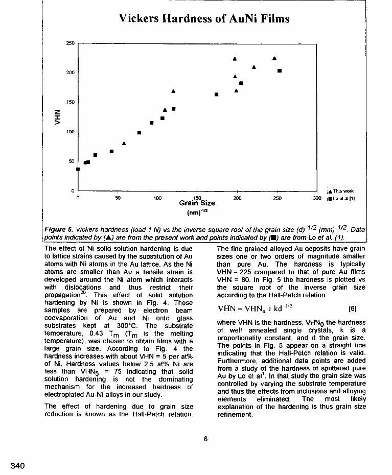
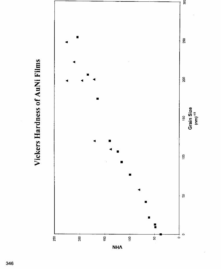
Figure 5. Vickers hardness (load 1 N) vs the inverse square root of the grain size (d)-lI2 (mm)-1’2. Data points indicated by (A) are from the present work and points indicated by (.) are from Lo et a/. (1).
The effect of Ni solid solution hardening is due to lattice strains caused by the substitution of Au atoms with Ni atoms in the Au lattice. As the Ni atoms are smaller than Au a tensile strain is developed around the Ni atom which interacts with dislocations and thus restrict their propagationz0. This effect of solid solution hardening by Ni is shown in Fig. 4. Those samples are prepared by electron beam coevaporation of Au and Ni onto glass substrates kept at 300°C. The substrate temperature, 0.43 Tm (Tm is the melting temperature), was chosen to obtain films with a large grain size. According to Fig. 4 the hardness increases with about VHN = 5 per at% of Ni. Hardness values below 2.5 at% Ni are less than VHN5 = 75 indicating that solid solution hardening is not the dominating mechanism for the increased hardness of electroplated Au-Ni alloys in our study.
The effect of hardening due to grain size reduction is known as the Hall-Petch relation.
The fine grained alloyed Au deposits have grain sizes one or two orders of magnitude smaller than pure Au. The hardness is typically VHN = 225 compared to that of pure Au films VHN = 80. In Fig. 5 the hardness is plotted vs the square root of the inverse grain size according to the Hall-Petch relation:
VHN = VHN, + kd ’” [el where VHN is the hardness, VHNO the hardness of well annealed single crystals, k is a proportionality constant, and d the grain size. The points in Fig. 5 appear on a straight line indicating that the Hall-Petch relation is valid. Furthermore, additional data points are added from a study yf the hardness of sputtered pure Au by Lo et al . In that study the grain size was controlled by varying the substrate temperature and thus the effects from inclusions and alloying elements eliminated. The most likely explanation of the hardening is thus grain size refinement.
_I
8
340

250
200
150
2 I >
1W
50
0
Vickers Hardness of AuNi Films
4
4
+
4
0 10 20 30 40 50 60 70 80 90 Interparticle Spacing
(10001nm)
Figure 6. Vickers hardness (load 1 N) vs inverse interparticle spacing (/)-I x I O3 (nm)-l.
Dispersion hardening due to the large number of inclusions in the Au-Ni deposits is also a possible Contribution’. Inclusion densities of the order of I O q 7 cmq3 (inclusion spacing of 20 nm) have been reported for alloyed gold deposits of hardness values ranging from 200 to 2302,3. As the inclusion density is difficult to control it has not been possible to distinguish between grain size and inclusion effects on the hardness. With the use of pulse plating, however, both the inclusion density and the grain size can be altered as a function of process parameters which makes it possible to make this separation.
The effect of inclusion density on the hardness is illustrated in Fig. 6 where hardness is plotted vs the inverse interparticle spacing. If the Orowan mechanism should be responsible for the increased hardness as discussed in reference 9, the data points should appear on a straight line sectioning the hardness axis close to VHN = 50. No such relation is seen in Fig. 6 and the hardness appears to be independent of the interparticle spacing. In Fig. 6 all particles are counted, regardless of size. However, the influence of dispersed particles on the hardness also depend on the particle size with a maximum found at particle sizes of typically 10
to 20 nm (20). In the films studied in this work, the interparticle spacing of such large particles is in the order of 40 to 50 nm, which is larger than the grain size of the deposits in question. It can thus be concluded that the main effect of the inclusions in alloyed Au films is of a grain refining nature. Their contribution to the hardness through dispersion hardening is minor compared to the contribution through grain size refinement.
To summarise the effect of pulse plating on the hardness of Au it has been shown that the Au becomes softer as the purity and, as a consequence, the grain size is increased. It has been argued that the wear properties is reduced of pulse plated hard-gold deposits [I I] which might be explained by the reduced hardness due to the improved punty.
SUMMARY
The composition of pulse plated Ni-alloyed Au can be controlled by varying the average current density and the duration of the current pulses. By increasing the average current density, the Ni content is lowered since Ni is the more noble metal of the two in this particular environment and, therefore, preferentially deposited at lower
9
34 1
current densities. By varying the duration of the pulses, the Ni content can be either lower or higher than by DC plating at the corresponding current density. When the current frequency is increased, the Ni content is also increased and reaches a maximum at a certain frequency. Above this maximum Ni have not sufficient time to diffuse back into the diffusion layer and Au is instead preferentially deposited resulting in a reduction in the Ni content.
The films show a fine grained microstructure with average grain sizes ranging from 16 to 26 nm. Non-crystalline inclusions at an inclusion spacing of about 20 nm are observed. However, when only an average thickness of 0.1 to 1 nm is deposited during each pulse, the inclusion spacing increases to at least 100 nm and the average grain sizes increase to about 70 to 90 nm. The material building up the inclusions is
most probably desorbed during the relaxation time if the latter is sufficiently long for the current to reach zero.
This study also conclusively shows that the hardness follows the Hall-Petch relation. Consequently, the increased hardness of Ni- alloyed Au is caused by grain size reduction rather than by solid solution hardening due to alloying with Ni or to dispersion hardening due to non-crystalline inclusions.
This study implies that a lot of care have to be taken when pulse plating is applied to enhance the wear properties of alloyed gold. However, for alloy deposition it is a superior technique for the control of alloy composition. Furthermore, pulse plating also offers a wide variety of other structural modifications and enhanced purity.
REFERENCES 13 H.T.G. Hentzell, B. Anderson, S-E Karlsson, Lo, J.A. Augis, M.R. Pinnel, J. Appl. Phys, - 50, 11 (November), 6887 (1979).
Willcox, J.R. Cady, Plating, 61, 12, 1117 (1974).
Darby, S.J. Harris, Trans. lnst. Metal. Finish., - 53, 138 (1975).
Tannenberger, K. Schindler, Proc. of AESF 3rd lnt. Pulse Plating Symposium, AESF, Orlando, FL (1 986) paper G.
Dossenbach, B. Stutzenegger, J.C. Puippe, Proc. of AESF 3rd lnt. Pulse Plating Symposium, AESF, Orlando, FL (1986) paper H.
G.B. Munier, Plating, 56, 10, 1151 (1969).
M. Antler, Plating, 60, 5, 468 (1973).
Ch.J. Raub, A. Knodler, J. Lendvay, Plat. Surf. Finish., 63, 1, 35 (1976).
Y. Okinaka, F.B. Koch, C. Wolowodiuk, D.R. Blessington, J. Electochem. SOC., 125, 11, 1745 (1978).
10 Y. Okinaka, S. Nakahara, J. Electrochem.
11 W.F. Fluhmann, F.H. Reid, P.A. Mausli. S.G.
SOC., 123, 9, 1284 (1976).
Steinemann, Plat. Surf Finish., 67, 6, 62 (1980).
Acta Metall., 3 l , 1131 (1983).
14 Y. Fukumoto, Y. Kawashima, I. Aoki, T. Hayashi, Proc. of AESF 3rd lnt. Pulse Plating Symposium, AESF, Orlando, FL (1 986) paper J.
15 N. Ibl, Metalloberfkche, 33, 2, 51 (1979).
16 D.S Lashmore, R. Oberle, M.P. Dariel, Proc. of AESF 3rd lnt. Pulse Plating Symposium, AESF, Orlando, FL (1986) paper J.
17 A.R. Despic, V.D. Jovic, J.Electrochem. SOC., 134, 12, 3004 (1987).
18 L.G. Holmbom, B.E. Jacobson, Plat. Surf. Finish., 74, 9, 74 (1987).
19 S. Nakahara, J. Crystal Growth, 75, 212 (1986).
20 P. Haasen, Physical Metallurgy, pp 323, Cambridge University Press, Cambridge (1978).
12 P.A. Mausli, F.H. Reid, S.Steinemann, MetallobeMache, 32, 9, 369 (1978).
10
342

at% Ni N
0 A
UI VI 4
0
\ \ \ \ \
I : I 1 : I I '
343
Current Density
344

Vickers hardness of PVD AuNi Films
120
100
80
z I > 60
40 - -
20 - -
0 ’
4 4 e 4 4 4 4 4
4 .-
e
- -
-~
- -
41
4 4 4
4
0 2 4 6 8
at% Ni 10 12 14
z 4 cw 0 m m aJ E
4
4 W
4
NHA
346

250
200
1 50
100
50
0 0
Vickers Hardness of AuNi Films
0
0 0
10
I ' I
20 30 40 50 60 Interparticle Spacing
(1 000/nm)
70 80 90
i i I