comparison of ccd damage due to 10 and 60 mev protons
TRANSCRIPT

Presented at the IEEE 2003 NSREC, Monterey, CA, July 2003. 1
Abstract-- Dark current and charge transfer inefficiency (CTI)
data are presented for four CCD device types after 9.5 and 60MeV proton irradiation. Comparison of the damage at the twoenergies allows a test of the validity of NIEL scaling. It wasfound that the ratio of the damage at 9.5 MeV to that at 60 MeVwas 35% higher for the CTI than for the average bulk darkcurrent, for the devices tested. Both the CTI and the darkcurrent showed significant annealing at 150°C.
I. INTRODUCTION
CCDs are especially vulnerable to proton-induceddisplacement damage and the effects have been extensivelystudied over the past decade [1]-[3]. However, there are anumber of issues that continue to be important. These include:- the nature of the lattice defects involved and the way the
defect inventory varies with particle type and energy- the corresponding variation in device properties (e.g.
dark signal and charge transfer inefficiency)- the nature of the defects responsible for dark current
fluctuations (Random Telegraph Signals) and thecharacteristics of the fluctuations and how they affectcalibration strategies for space instruments.
Knowledge of the types of lattice defects created by protonirradiation is particularly important for space scienceinstruments that operate the CCD at low temperatures. This isbecause the main defects responsible for charge transfereffects near room temperature can be 'frozen out' by keepingthem filled with charge (for example, using LED pre-flashingor charge injection from special input gate structures [4]). Thefaster traps are still active, however, and tend to dominate theradiation effects in the CCD, but, so far, we have littleknowledge of the defects involved or how the trapconcentrations may vary with proton energy or the materialscomposition of the silicon wafer.
The starting point for making device damage calculations isto assume that the damage is proportional to the nonionizingenergy loss (NIEL) [5]. This is equivalent to assuming thatthe relative trap concentrations do not change with proton
Manuscript received July 22, 2003. This work was funded by the
European Space Agency.Gordon Hopkinson is with Sira Electro-Optics Ltd, South Hill,
Chislehurst, Kent, BR7 5EH, UK (telephone +44 (0)208 468 1794, e-mail:[email protected]).
Ali Mohammadzadeh is with the European Space Agency, ESTEC,Keplerlaan 1, 2200 AG, Noordwijk, The Netherlands (telephone + 31 71 5655894), e-mail [email protected].
energy. NIEL scaling has been observed to hold reasonablywell for many devices and, in particular, for CCD chargetransfer inefficiency (CTI) [6] and mean dark signal [7].Hence NIEL scaling is a good first step for damage predictionand allows for most of the damage dependence on particletype and energy. However there is still the possibility thatNIEL scaling may not apply at a detailed level.
Recent calculations of the nonionizing energy loss insilicon have been presented by Dale et al. [8], Akkerman etal. [9] and Jun et al. [10]. Whilst consistent, considering theuncertainties involved, there are some important differences.In particular the ratio between the NIEL values at 10 and 60MeV is 3.3 from [9] compared to 2.2 in the Dale et al data.These two energies are important since 10 MeV is often usedfor ground testing (because of the irradiation facilitiesavailable and because of the ease of masking the device intoseveral fluence regions), whilst protons of energy around 60MeV predominate in the space environment inside spacecraft(the low energy protons having been removed by shielding).Hence it would be useful to know which value is correct – oreven if the same ratio holds for both dark current and chargetransfer damage (or for different device types).
The present study arose from a radiation evaluation ofseveral CCD types in support of a programme of theEuropean Space Agency (ESA) for Capability Approval ofCCD suppliers. Since the programme called for an extensivedevice study, the opportunity was taken to use the data toconsider further the relation between dark current and CTIdamage and the nonionizing energy loss. Although the factor1.5 discrepancy in NIEL, mentioned above, may seem small,the CCD displacement damage is often critical to missionlifetime and it is important that design margins are not overlyconservative. It is hoped that the results of the study will alsogive some insight into mechanisms of defect generation.
To measure damage ratios accurately it was consideredimportant to irradiate with the two proton energies on thesame device. Otherwise any variation in device-to-deviceresponse or in test or operating conditions might mask anydifferences. This was a contributing factor in deciding thehighest energy which could be used during this investigation.At 60 MeV it is just possible to shield the device so that partis unirradiated (and so can be used as a reference and/or forlater irradiation at a lower energy). It will be seen that theproduction of secondary protons and neutrons (due tointeraction of the primary protons with the material of the
Comparison of CCD Damage due to 10 and 60MeV Protons
Gordon R. Hopkinson, Member, IEEE and Ali Mohammadzadeh

Presented at the IEEE 2003 NSREC, Monterey, CA, July 2003. 2
masking shield) gives significant effects – which are expectedto be yet more pronounced should a higher energy be used.9.5 MeV was chosen as the lower energy so that a comparisoncould be made with the substantial amount of existing testdata at that energy. Note that in future programs (when agreater number of device samples may be available) it wouldbe useful to perform additional damage comparisons at bothlower and higher energies (e.g. 1.5 and 100 MeV).
At 9.5 MeV most recoil atoms have low energy and thedamage is mainly in point defects; whereas at 60 MeVinelastic collisions are more common, recoil energies arehigher and there are far more clusters (see [1] and thereferences therein and [11]). Hence, if there are anysignificant differences in defect character between point andcluster damage then this should be apparent in the results.
As well as making a comparison of damage at the twoenergies, this study also provides a database of damageeffects [12]. By measuring trap emission times at severaltemperatures it is possible to gain some insight into device-to-device differences in trap concentration. Results of hightemperature annealing will also be discussed. It will be seenthat significant annealing of both dark current and CTI occursabove 100°C.
The opportunity was taken to study the random telegraphsignal (RTS) behavior in the proton-irradiated CCDs(particularly for some devices which were irradiated to a lowfluence of 9.5 MeV protons so that the chance of more thanone RTS defect in a pixel is small and the RTS signals arerelatively clear) – however this was not the main focus of thestudy. This work provides an update to previous studies butcannot be claimed to be an in-depth investigation (which isstill required if accurate predictions of occurrenceprobabilities and temperature behavior are to be made).
Cobalt60 irradiations were also performed on devices ofeach type so as to give information on total ionizing doseeffects. The results will be discussed briefly.
II. EXPERIMENTAL
A. Irradiations
The 60 MeV irradiations were carried out at the PaulScherer Institute (PSI), Switzerland and the 9.5 MeV at EbisIotron Ltd, Harwell UK. These irradiations were unbiased(pins shorted) with the CCDs at room temperature. Thedevices were masked to produce unirradiated regions (at 60MeV 8 mm steel was used and at 9.5 MeV, 1.5 mmaluminum). The 60 MeV fluence was 5.9 1010 p/cm2 and for9.5 MeV was 1.7 1010 p/cm2. In addition, some devices wereirradiated at 9.5 MeV to several fluence levels (up to 3.4 1010
p/cm2). The cobalt60 irradiations were done at ESA ESTEC,under both biased (normal clocked operation) and unbiasedconditions, at room temperature and at a dose rate ~3krd(Si)/hr. In all cases, dosimetry was performed by thefacility staff and is believed to be accurate to better than ±5%.All the irradiations were carried out during May-October2002. Measurements were typically carried out 1 week after
irradiation and checked again after several months storage atroom temperature. There was no significant annealing ofCCD parameters at room temperature and this annealing willnot be discussed further.
B. Devices
The devices tested, all frame transfer CCDs, aresummarized below. The pixel numbers are for the imageregion (there are an equal number in the storage region, whichwas shielded from light during use). All except the CCD55-20had a front illuminated architecture:- CCD55-20: 770 x 576, 22.5 µm x 22.5 µm pixels from e2v
Technologies, Chelmsford, UK. Advanced inverted modeoperation (AIMO).
1 device 9.5 and 60 MeV protons1 device cobalt60, biased to 18 krd(Si)
- CCD57-10: 512 x 512, 13 µm x 13 µm pixels withantiblooming structures from e2v Technologies, operatedwith 2 of the 3 clock phases inverted.
2 devices 9.5 and 60 MeV protons1 device 9.5 MeV protons1 device cobalt60, biased to 18 krd(Si)
1 device co60, biased 18 krd(Si) + 18 krd(Si) unbiased- TH7890M 512 x 512 17 µm x 17 µm pixels from Atmel,
France, inverted (MPP) mode2 devices 9.5 and 60 MeV protons2 devices 9.5 MeV protons1 device cobalt60, biased to 13 krd(Si)1 device cobalt60, unbiased to 18 krd(Si)
The CCD55-20 was not used for CTI measurements as itsinverted mode structure did not allow backwards clocking anduse of the FPR technique Tests were also made on AtmelTH7863D CCDs (288 x 384, 23 µm x 23 µm pixels) but thesewere not irradiated at two energies and results will not bediscussed in detail. (see [12] for further information).
C. Device Testing
Devices were tested using equipment supplied by SiraElectro-optics Ltd. This included camera electronics whichallowed computer control of biases and clock sequences anddigitization of the signals to 16 bit. Image Pro Plus softwarewas used for image analysis and Agilent Vee Pro forautomatic test sequences.
The devices were mounted in a liquid nitrogen cooleddewar with a heater mounted on a copper heatsink behind thedevice. This allowed control of the CCD temperature to±0.1°C over the range -120 to 30°C (measured with acalibrated platinum resistor mounted in the heatsink).
Measurements of dark current were made on the average of16 images to reduce noise. CTI measurements used the firstpixel response FPR method [13],[15]. There are limitations tothis technique when the CTI is large and care was taken thatdata was only used for which the proportional charge loss wassmall (i.e. avoiding data for very low signal levels).
For both dark current and CTI a damage factor can bedefined using

Presented at the IEEE 2003 NSREC, Monterey, CA, July 2003. 3
Device damage = damage factor x DD. (1)
Where DD is the displacement damage dose, that is, theproduct of the NIEL and the particle fluence.
In all cases the digitized CCD signals (in ADC units) wereconverted to electrons/pixel using the data derived fromCd109 X-ray calibrations (made before and after theirradiations).
III. RESULTS
A. Proton-induced Dark Signal
Fig. 1 shows a horizontal profile (averaged over severalhundred columns) across a 9.5/60 MeV irradiated CCD57-10device. The ionization-induced dark current (determined fromthe separate cobalt60 irradiation) was small and the factor 2difference between the average dark current in the tworegions (after allowing for the differences in proton fluence)gives a ratio between the damage at 9.5 MeV and that at 60MeV of 1.74 ± 0.1. It can also be seen that the 60 MeVregion has ‘soft’ boundaries due to the effect of interactionsof the proton beam with the 8 mm steel mask. This limits thedevice area that can be used for measurements. The damagefactor ratios were similar in the other device types. If weassume a 4% change in extrapolating from 9.5 MeV to 10MeV (based on the data of [8]) then the dark current damageratios are as given below:
Dark current damage at 10 MeV/damage at 60 MeVCCD55-20 (1 device) 1.67 ± 0.3CCD57-10 (2 devices) 1.67 ± 0.3
TH7890M (2 devices) 1.86 ± 0.3
It was found that the irradiations at 9.5 MeV all gave verysimilar dark currents for devices of the same type, Fig. 2 givessome examples of dark current histograms. In all cases theaverage dark charge and the main peak of the histogramsscaled with temperature with an activation energy in the range0.63 to 0.65 eV as expected, but there is significant fieldenhancement (lowering of activation energy for the largerdark current spikes) as shown in the example of Fig 3.
Since there was significant field enhancement, the damagehistograms were not used to derive the damage constant (as inthe method of Marshall [16] and Robbins [17]). Instead theaverage dark current level was used and the following valuesobtained (the error values were derived from estimates of themeasurement and dosimetry errors):
Damage constant for bulk dark currentelectrons/cm3/(MeV/g) at 300 K
CCD55-20 (3.4 ±0.7) 105
CCD57-10 (1.6 ±0.7) 105
TH7890M (1.4 ±0.7) 105
These values can be compared with the universal damageconstant proposed by Srour and Lo [18]. They give a value of(1.9 ±0.6) 105 electrons/cm3/(MeV/g) at 300 K which is ingood agreement with the above. Note that, to derive the
damage constants, an estimate of the active volume is needed.The values used were:
0
5000
10000
15000
20000
0 100 200 300 400 500
Column Number
Dar
k S
ign
al D
ensi
ty (
AD
U)
Shielded8 mm Steel (60 MeV)1.5 mm Al (9.5 MeV)
CCD57-10 #1After 9.5 and 60 MeV proton Irradiation60 MeV
9.5 MeV
Fig 1 Horizontal profile across a dark image for a CCD57 irradiated with9.5 and 60 MeV protons
0.1
1
10
100
1000
0 10000 20000 30000 40000 50000 60000
Dark Signal Density, Normalized to 20.0°C (electrons/pixel/s)
Co
un
t
CCD #6, 10 krd, 9.5 MeV, 28.9°CCCD #2, 10krd, 9.5 MeV, 24.7°CCCD #2, 8 krd, 60 MeV, 24.7°CCCD #3, 10 krd, 9.5 MeV, 28.0°CCCD #1, 10 krd, 9.5 MeV, 28.5°CCCD #1, 8 krd, 60 MeV, 28.5°CCCD #1, 10 krd, 9.5 MeV, -20.0°C
Atmel TH7890M
Fig 2 Dark current histograms for Atmel TH7890M devices. The data fordevice 1 was obtained at both 28.6°C and -20.0°C. The low temperaturedark signal density has been scaled assuming an activation energy of 0.63eV so that it overlays the plot at 28.6°C.
0.30
0.35
0.40
0.45
0.50
0.55
0.60
0.65
0.70
0 10000 20000 30000 40000 50000 60000 70000 80000
Dark Signal at 20°C (electrons/pixel/s)
Act
ivat
ion
En
erg
y (e
V)
e2v CCD57-10 #5After 1.7 1010 9.5 MeV p/cm2
Fig. 3 Activation energy for an e2v CCD57-10 device, measured over therange -40OC to 28°C.
CCD active volume (µm3)CCD55-20 1500 (22.5 µm x 16.5 µm x 4 µm)CCD57-10 500 (13 µm x 9 µ m x 4 µm)TH7890M 750 (17 µm x 11 µm x 4 µm)
One CCD57-10 and one TH7890M device were given ananneal by baking for 3 days at 83°C, then at 110°C and finallyat 150°C. The effects in both devices were very similar. Darkcurrent histograms for the TH7890M CCD are shown in Fig.4. It is seen that there is a significant reduction in the dark

Presented at the IEEE 2003 NSREC, Monterey, CA, July 2003. 4
signal nonuniformity, particularly after the final annealingstage at 150°C. Fig 5. Show the estimated annealing factors,which were derived by scaling plots of the horizontal darkcurrent profile (such as Fig 2) so that they could be overlayed.This scaling was found to apply to both the 9.5 and 60 MeVregions, although in the e2v CCD57-10 device the 60 MeVregion showed somewhat increased annealing during the final150°C bake (though since this device was not operated fullyinverted, there may be a small contribution due to surfacedark current). Also shown in Fig. 5 are results for the chargetransfer inefficiency (CTI), which will be discussed later.Annealing of bulk dark current at temperatures in the range100-150°C has also been observed by Holland [19].
Based on the similarity of the damage constant for a widevariety of devices, Srour and Lo [18] suggested that devicedark current is unlikely to be caused by an impurity relateddefect but may be due to the divacancy or a multiple vacancycomplex. The annealing behavior described above wouldseem to eliminate the divacancy (since it does not anneal until~ 300°C [20]) but a higher order vacancy is not ruled out.Another argument against the divacancy (V2) is that its level,at ~0.43 eV is some way from mid-gap and it is not anefficient generator of dark current. (These arguments havealso been put forward by Robbins [17].) In fact, applyingstandard Shockley Read Hall generation theory [21] withequal hole and electron emission cross sections (σp and σn),gives a factor 100 difference in generation rate between amidgap state and the divacancy. Mid-gap defects having anenergy level ~ 0.55 eV have been found previously butannealing data is either unavailable or ambiguous. Schmidt etal. [22],[23] suggested that their 0.56 eV level is amultivacancy defect but could only confirm that the defecthad annealed by 350°C. Ahmed et al. [24] found a defect inproton-irradiated silicon diodes that anneals at around 170°Cand tentatively identified it as the four-vacancy (V4) becauseof its annealing temperature, though they suggested an energylevel of 0.37 eV. Pintille et al [25] also found a level at ~ 0.55eV but identified it as related to the V2O complex. Howeverthe V2O defect is known to be stable up to roughly 300°C[20] and so cannot be the main defect responsible for CCDbulk dark current. There is other evidence that there areradiation-induced defects which anneal at around 150°C[26],[27] and these are often associated with the electronparamagnetic resonance (EPR) P3 and P6 centers. These areoften identified as the V4 and di-interstitial (I2) centers,respectively, but these identifications (and the associatedenergy levels) are not conclusive (at least in the case of the I2
[28]). Troxell [29] found a Ev+0.53 eV defect in p-typesilicon which annealed at ~150°C but the defect was notidentified. It should also be noted that many studies have notfound mid-gap defects and it can only be concluded that thereare many inconsistencies in the literature. Another feature tobear in mind is that many of the proton-induced dark currentdefects are metastable and give rise to random telegraphsignal (RTS) fluctuations [30] as discussed in the next
section. Metastable behavior in intrinsic defects has beensuggested (e.g. in the V2 [31]and I2 [32]) but, again, theevidence is not conclusive.
0.1
1
10
100
1000
0 10000 20000 30000 40000 50000 60000
Dark Signal Density, Normalized to 20.5°C (electrons/pixel/s)
Co
un
t
Atmel TH7890M1.71010 9.5 MeV p/cm2Pre-anneal
After Second Anneal
After Third Anneal
Fig. 4 Dark signal histograms after annealing. The annealing steps were 3days at 83°C (not shown), followed by 3 days at 110°C and then 150°C.
0
0.2
0.4
0.6
0.8
1
60 80 100 120 140 160
Annealing Temperature (°C)
An
nea
ling
Fac
tor
TH7890M #1
Dark Signal
CTI
CCD57 #1
Pre-anneal Value
Fig.5 Annealing factors for average bulk dark current, filled symbols (andCTI, open symbols) for the three annealing steps of 83°C, 110°C and 150°C(3 days at each). CCD57: triangles, TH7890M, circles.
0
500
1000
1500
2000
2500
3000
3500
4000
4500
0 10000 20000 30000 40000 50000 60000 70000
Average Signal (ADU, 1 ADU = 0.76 electrons))
RM
S S
ign
al (
AD
U)
RTS PixelsTH7890M #61.7 1010 9.5 MeV p/cm2
28.5°C
700 ms Integration Time250 random Samples
Fig. 6 Identification of RTS pixels for a TH7890M device
B. Measurements of Random Telegraph Signals
For proton irradiated devices some of the defects showmetastable behavior so that the dark signal switches betweenwell defined levels, giving the appearance of a randomtelegraph signal (RTS). This has been studied previously [30]for a limited number of pixels. In this study it was possible tofollow sets of several hundred pixels and to analyze thesignals at several CCD temperatures. Fig. 6 shows the root

Presented at the IEEE 2003 NSREC, Monterey, CA, July 2003. 5
mean square (RMS) signal for a sample of 250 pixels taken atrandom from the 1.7 1010 p/cm2 region of a 9.5 MeV protonirradiated TH7890M. RTS defects can readily be identified asthey lie above the shot noise baseline. At this radiation levelmost pixels show RTS effects. Fig. 7 shows a similar plot fora CCD57-10 device, irradiated to ~ 5 108 9.5 MeVprotons/cm2. In this case the dosimetry was rather uncertainand so it was not possible to derive accurate occurrenceprobabilities, but the number of RTS defects (six in this case)is consistent with the 0.000016 RTS defects/proton/pixeloriginally found [30]. Other data (so far unpublished) is alsoconsistent with this occurrence probability.
As in previous investigations, some high dark currentpixels do not show RTS effects. Fig 8 shows RTS plots at -40°C, so far the lowest temperature at which they have beenobserved in ground testing - though inflight data [33] suggeststhat the phenomenon can occur down to much lowertemperatures. In this study it was found that the RTSamplitudes varied with temperature with an activation energyof roughly 0.6 eV. The switching time constants were notstudied in detail, but the data is consistent with activationenergies of 0.9 to 1.6 eV, so that at low temperatures the timeconstants can be several hours or even days.
0
200
400
600
800
1000
1200
0 1000 2000 3000 4000 5000
Average Signal (ADU/pixel/s, 1 ADU = 0.67 electrons)
RM
S S
ign
al (
AD
U)
CCD57-10 #5~ 5 108 9.5 MeV protons/cm2
10.3°C, 1s Integration Time220 Random Pixels
RTS Pixels
Fig 7. Identification of RTS pixels for a CCD57-10 device
0
100
200
300
400
500
600
700
800
900
0 2 4 6 8 10 12
Time (Hours)
Sig
nal
(A
DU
)
CCD57 #5, -40°C, 20 s Integration Time, 1 ADU = 0.67 electrons
Fig 8. RTS fluctuations at -40°C for a CCD57-10. The CCD integration timewas 20s and 1 ADC unit (ADU) corresponded to 0.67 electrons.
The number of RTS pixels decreased after the 3 dayanneals at 83°C, 110°C and 150°C (for both the CCD57-10and TH7890M devices studied). The largest decrease beingafter the 150°C bake after which nearly all the RTSfluctuations had disappeared (though 2 or three RTS pixelsstill remained -in samples of 250 random pixels from the 1.7
1010 9.5 MeV p/cm2 regions). Hence it is concluded that theRTS pixels show much the same annealing behavior as theaverage bulk dark current, though the data indicates thatannealing was more pronounced for RTS since nearly all thedefects were annealed, whereas Fig.5 shows that there is stilla significant component remaining for the average darksignal.
C. Measurements of CTI
Fig. 9 shows measurements of trap emission time at severaltemperatures for both the 9.5 and 60 MeV regions of a typicaldevice. These were made at the same signal level andbackground. To scale the damage so that the plots coincided,a ratio of 1.47 ±0.02 was found to apply for all the devices(and in fact for all the CTI measurements at other signallevels, backgrounds and temperatures). That is, the CTI forthe 60 MeV region was always greater than that in the 9.5MeV region by a factor of roughly 1.5. This suggests that theinventory of traps was not significantly different between the9.5 and 60 MeV regions.
0
0.0002
0.0004
0.0006
0.0008
0.001
0.0012
0.0014
0 20 40 60 80 100
Delay Time Between Injection and Signal (unit = 0.6 ms)
Ver
ticv
al C
TI
Atmel TH7890M CCD #1
-40°C
-60°C
-50°C
1.7 1010 9.5 MeV p/cm2
5.9 1010 60 MeV p/cm2, CTI divided by 1.47
Fig. 9 Trap emission times were found by measuring the CTI as a function ofthe delay time used in the first pixel response measurement. Dividing the 60MeV data by 1.47 allowed the plots to be overlapped and this gives anestimate of the ratio between the CTI damage at 9.5 and 60 MeV.
Taking into account the difference in fluence (5.9 1010
p/cm2 at 60 MeV and 1.7 1010 p/cm2) and, as for the averagedark signal, a 4% change in extrapolating from 9.51 to 10MeV, this gives a damage factor ratio (CTI at 10 MeVdivided by that at 60 eV) of 2.27 ± 0.1, very close to theexpectation from Dale et al but slightly (and significantly)different from the ratio for dark current. Note that, althoughdosimetry errors will affect the damage ratio, these errors willbe the same for both the dark signal and CTI measurementsand so the difference in damage ratio (roughly 1.7 for darksignal and 2.3 for CTI) is significant.
Fig 5. Showed the CTI annealing data. This was obtainedby plotting CTI as a function of signal and background andapplying scaling factors so that the plots could be overlapped.It was found that a single scaling factor could be used for allsignals and backgrounds (that is, the same factor could beused to scale between two annealing steps independent of theparticular signal and background conditions used for both thefluence regions). During the annealing the relative
Presented at the IEEE 2003 NSREC, Monterey, CA, July 2003. 6
proportions of the traps did not seem to change appreciably;i.e. they seemed to anneal together.
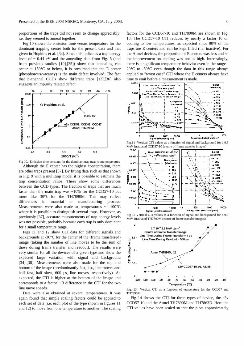
Fig 10 shows the emission time versus temperature for thedominant trapping center both for the present data and thatgiven in Hopkins et al. [34]. Since this indicates a trap energylevel of ~ 0.44 eV and the annealing data from Fig. 5 (andfrom previous studies [19],[35]) show that annealing canoccur at 150°C or below, it is presumed that the E center(phosphorous-vacancy) is the main defect involved. The factthat p-channel CCDs show different traps [13],[36] alsosuggests an impurity related defect.
0.01
0.1
1
10
100
1000
3.4 3.9 4.4 4.9 5.4
1000/T (K-1)
Em
issi
on
Tim
e C
on
stan
t (m
s)
Hopkins et al.
20 0 -20 -40 -60 -80 -100
0.440 eV
-50 -70 -90
e2v CCD57, CCD02, CCD47 Atmel TH7890M
Fig 10. Emission time constant for the dominant trap near room temperature
Although the E center has the highest concentration, thereare other traps present [37]. By fitting data such as that shownin Fig. 9 with a multitrap model it is possible to estimate thetrap concentration ratios. These show some differencesbetween the CCD types. The fraction of traps that are muchfaster than the main trap was ~10% for the CCD57-10 butmore like 30% for the TH7890M. This may reflectdifferences in material or manufacturing process.Measurements were also made at temperatures ~ -100°Cwhere it is possible to distinguish several traps. However, aspreviously [37], accurate measurements of trap energy levelswas not possible, probably because each trap is only dominantfor a small temperature range.
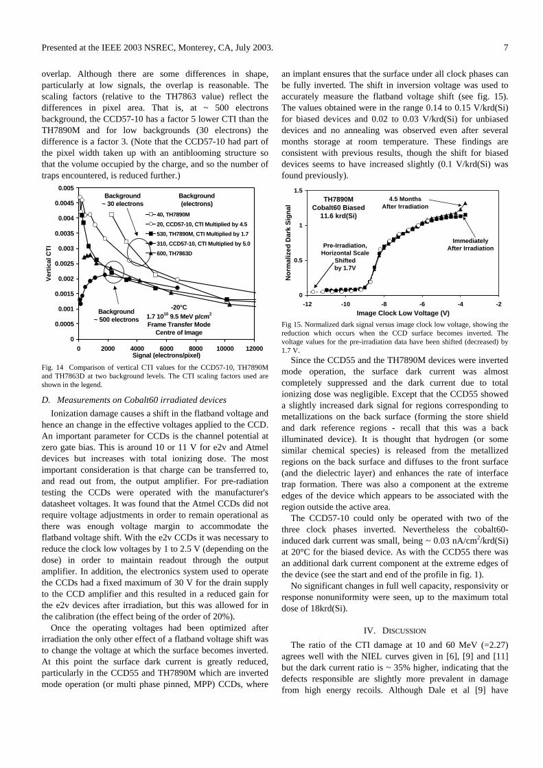
Figs 11 and 12 show CTI data for different signals andbackgrounds at -30°C for the center of the (frame transferred)image (taking the number of line moves to be the sum ofthose during frame transfer and readout). The results werevery similar for all the devices of a given type and show theexpected large variation with signal and background[34],[38]. Measurements were also made for the top andbottom of the image (predominantly fast, 4µs, line moves andhalf fast, half slow, 600 µs, line moves, respectively). Asexpected, the CTI is higher at the bottom of the image andcorresponds to a factor ~ 3 difference in the CTI for the twoline move speeds.
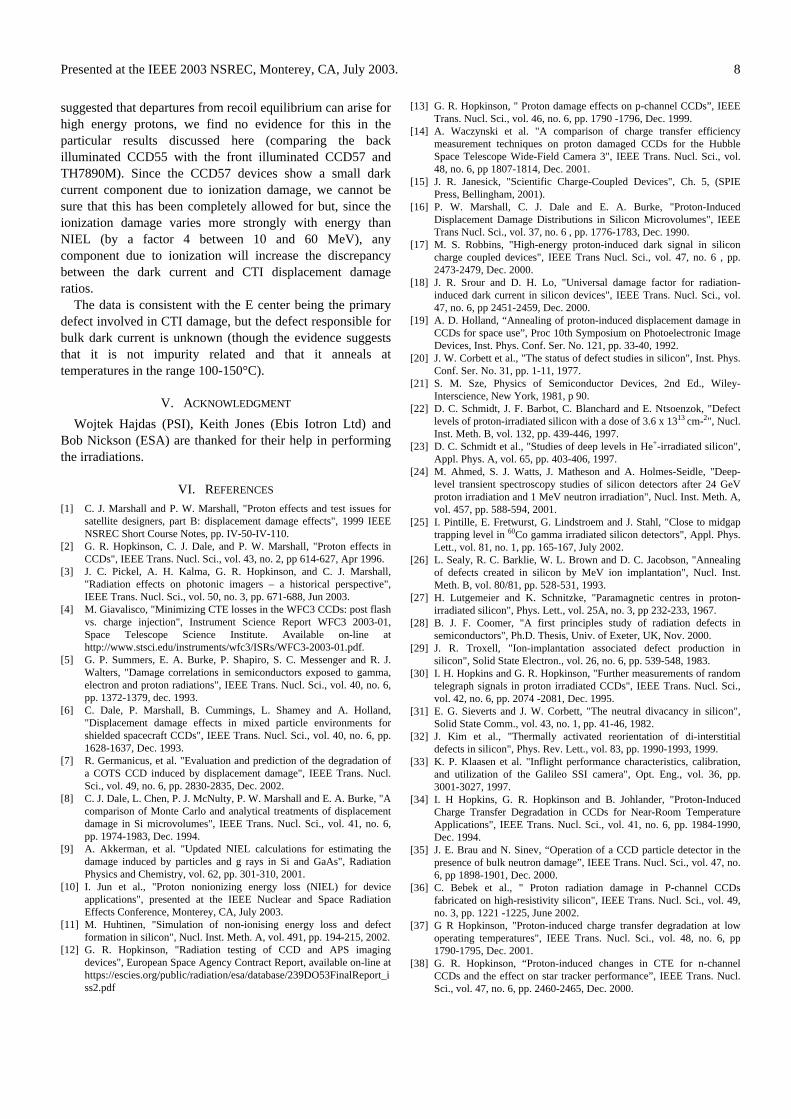
Data were also obtained at several temperatures. It wasagain found that simple scaling factors could be applied toeach set of data (i.e. each plot of the type shown in figures 11and 12) to move from one temperature to another. The scaling
factors for the CCD57-10 and TH7890M are shown in Fig.13. The CCD57-10 CTI reduces by nearly a factor 10 oncooling to low temperatures, as expected since 90% of thetraps are E centers and can be kept filled (i.e. inactive). Forthe Atmel devices, the proportion of E centers was less and sothe improvement on cooling was not as high. Interestingly,there is a significant temperature behavior even in the range -20°C to -50°C even though the data in this range alwaysapplied to "worst case" CTI where the E centers always havetime to emit before a measurement is made.
Fig.11 Vertical CTI values as a function of signal and background for a 9.5MeV irradiated CCD57-10 (centre of frame transfer images)
Fig 12 Vertical CTI values as a function of signal and background for a 9.5MeV irradiated TH7890M (centre of frame transfer images)
0
0.5
1
1.5
2
-120 -110 -100 -90 -80 -70 -60 -50 -40 -30 -20 -10
Temperature (°C)
CT
I Sca
ling
Fac
tor
1.7 1010 9.5 MeV p/cm2
Centre of Frame Transfer Image Line Time During Frame Transfer = 4 µs
Line Time During Readout = 580 µs
e2V CCD57-10, #1, #2, #5
Atmel TH7890M, #2
Fig. 13 Vertical CTI as a function of temperature for the CCD57 andTH7890M.
Fig 14 shows the CTI for three types of device, the e2vCCD57-10 and the Atmel TH7890M and TH7863D. Here theCTI values have been scaled so that the plots approximately
Presented at the IEEE 2003 NSREC, Monterey, CA, July 2003. 7
overlap. Although there are some differences in shape,particularly at low signals, the overlap is reasonable. Thescaling factors (relative to the TH7863 value) reflect thedifferences in pixel area. That is, at ~ 500 electronsbackground, the CCD57-10 has a factor 5 lower CTI than theTH7890M and for low backgrounds (30 electrons) thedifference is a factor 3. (Note that the CCD57-10 had part ofthe pixel width taken up with an antiblooming structure sothat the volume occupied by the charge, and so the number oftraps encountered, is reduced further.)
0
0.0005
0.001
0.0015
0.002
0.0025
0.003
0.0035
0.004
0.0045
0.005
0 2000 4000 6000 8000 10000 12000Signal (electrons/pixel)
Ver
tica
l CT
I
40, TH7890M
20, CCD57-10, CTI Multiplied by 4.5
530, TH7890M, CTI Multiplied by 1.7
310, CCD57-10, CTI Multiplied by 5.0
600, TH7863D
-20°C1.7 1010 9.5 MeV p/cm2
Frame Transfer ModeCentre of Image
Background (electrons)
Background ~ 30 electrons
Background ~ 500 electrons
Fig. 14 Comparison of vertical CTI values for the CCD57-10, TH7890Mand TH7863D at two background levels. The CTI scaling factors used areshown in the legend.
D. Measurements on Cobalt60 irradiated devices
Ionization damage causes a shift in the flatband voltage andhence an change in the effective voltages applied to the CCD.An important parameter for CCDs is the channel potential atzero gate bias. This is around 10 or 11 V for e2v and Atmeldevices but increases with total ionizing dose. The mostimportant consideration is that charge can be transferred to,and read out from, the output amplifier. For pre-radiationtesting the CCDs were operated with the manufacturer'sdatasheet voltages. It was found that the Atmel CCDs did notrequire voltage adjustments in order to remain operational asthere was enough voltage margin to accommodate theflatband voltage shift. With the e2v CCDs it was necessary toreduce the clock low voltages by 1 to 2.5 V (depending on thedose) in order to maintain readout through the outputamplifier. In addition, the electronics system used to operatethe CCDs had a fixed maximum of 30 V for the drain supplyto the CCD amplifier and this resulted in a reduced gain forthe e2v devices after irradiation, but this was allowed for inthe calibration (the effect being of the order of 20%).
Once the operating voltages had been optimized afterirradiation the only other effect of a flatband voltage shift wasto change the voltage at which the surface becomes inverted.At this point the surface dark current is greatly reduced,particularly in the CCD55 and TH7890M which are invertedmode operation (or multi phase pinned, MPP) CCDs, where
an implant ensures that the surface under all clock phases canbe fully inverted. The shift in inversion voltage was used toaccurately measure the flatband voltage shift (see fig. 15).The values obtained were in the range 0.14 to 0.15 V/krd(Si)for biased devices and 0.02 to 0.03 V/krd(Si) for unbiaseddevices and no annealing was observed even after severalmonths storage at room temperature. These findings areconsistent with previous results, though the shift for biaseddevices seems to have increased slightly (0.1 V/krd(Si) wasfound previously).
0
0.5
1
1.5
-12 -10 -8 -6 -4 -2
Image Clock Low Voltage (V)
No
rmal
ized
Dar
k S
ign
al
Pre-Irradiation, Horizontal Scale
Shifted by 1.7V
TH7890MCobalt60 Biased
11.6 krd(Si)
Immediately After Irradiation
4.5 Months After Irradiation
Fig 15. Normalized dark signal versus image clock low voltage, showing thereduction which occurs when the CCD surface becomes inverted. Thevoltage values for the pre-irradiation data have been shifted (decreased) by1.7 V.
Since the CCD55 and the TH7890M devices were invertedmode operation, the surface dark current was almostcompletely suppressed and the dark current due to totalionizing dose was negligible. Except that the CCD55 showeda slightly increased dark signal for regions corresponding tometallizations on the back surface (forming the store shieldand dark reference regions - recall that this was a backilluminated device). It is thought that hydrogen (or somesimilar chemical species) is released from the metallizedregions on the back surface and diffuses to the front surface(and the dielectric layer) and enhances the rate of interfacetrap formation. There was also a component at the extremeedges of the device which appears to be associated with theregion outside the active area.
The CCD57-10 could only be operated with two of thethree clock phases inverted. Nevertheless the cobalt60-induced dark current was small, being ~ 0.03 nA/cm2/krd(Si)at 20°C for the biased device. As with the CCD55 there wasan additional dark current component at the extreme edges ofthe device (see the start and end of the profile in fig. 1).
No significant changes in full well capacity, responsivity orresponse nonuniformity were seen, up to the maximum totaldose of 18krd(Si).
IV. DISCUSSION
The ratio of the CTI damage at 10 and 60 MeV (=2.27)agrees well with the NIEL curves given in [6], [9] and [11]but the dark current ratio is ~ 35% higher, indicating that thedefects responsible are slightly more prevalent in damagefrom high energy recoils. Although Dale et al [9] have
Presented at the IEEE 2003 NSREC, Monterey, CA, July 2003. 8
suggested that departures from recoil equilibrium can arise forhigh energy protons, we find no evidence for this in theparticular results discussed here (comparing the backilluminated CCD55 with the front illuminated CCD57 andTH7890M). Since the CCD57 devices show a small darkcurrent component due to ionization damage, we cannot besure that this has been completely allowed for but, since theionization damage varies more strongly with energy thanNIEL (by a factor 4 between 10 and 60 MeV), anycomponent due to ionization will increase the discrepancybetween the dark current and CTI displacement damageratios.
The data is consistent with the E center being the primarydefect involved in CTI damage, but the defect responsible forbulk dark current is unknown (though the evidence suggeststhat it is not impurity related and that it anneals attemperatures in the range 100-150°C).
V. ACKNOWLEDGMENT
Wojtek Hajdas (PSI), Keith Jones (Ebis Iotron Ltd) andBob Nickson (ESA) are thanked for their help in performingthe irradiations.
VI. REFERENCES
[1] C. J. Marshall and P. W. Marshall, "Proton effects and test issues forsatellite designers, part B: displacement damage effects", 1999 IEEENSREC Short Course Notes, pp. IV-50-IV-110.
[2] G. R. Hopkinson, C. J. Dale, and P. W. Marshall, "Proton effects inCCDs", IEEE Trans. Nucl. Sci., vol. 43, no. 2, pp 614-627, Apr 1996.
[3] J. C. Pickel, A. H. Kalma, G. R. Hopkinson, and C. J. Marshall,"Radiation effects on photonic imagers – a historical perspective",IEEE Trans. Nucl. Sci., vol. 50, no. 3, pp. 671-688, Jun 2003.
[4] M. Giavalisco, "Minimizing CTE losses in the WFC3 CCDs: post flashvs. charge injection", Instrument Science Report WFC3 2003-01,Space Telescope Science Institute. Available on-line athttp://www.stsci.edu/instruments/wfc3/ISRs/WFC3-2003-01.pdf.
[5] G. P. Summers, E. A. Burke, P. Shapiro, S. C. Messenger and R. J.Walters, "Damage correlations in semiconductors exposed to gamma,electron and proton radiations", IEEE Trans. Nucl. Sci., vol. 40, no. 6,pp. 1372-1379, dec. 1993.
[6] C. Dale, P. Marshall, B. Cummings, L. Shamey and A. Holland,"Displacement damage effects in mixed particle environments forshielded spacecraft CCDs", IEEE Trans. Nucl. Sci., vol. 40, no. 6, pp.1628-1637, Dec. 1993.
[7] R. Germanicus, et al. "Evaluation and prediction of the degradation ofa COTS CCD induced by displacement damage", IEEE Trans. Nucl.Sci., vol. 49, no. 6, pp. 2830-2835, Dec. 2002.
[8] C. J. Dale, L. Chen, P. J. McNulty, P. W. Marshall and E. A. Burke, "Acomparison of Monte Carlo and analytical treatments of displacementdamage in Si microvolumes", IEEE Trans. Nucl. Sci., vol. 41, no. 6,pp. 1974-1983, Dec. 1994.
[9] A. Akkerman, et al. "Updated NIEL calculations for estimating thedamage induced by particles and g rays in Si and GaAs", RadiationPhysics and Chemistry, vol. 62, pp. 301-310, 2001.
[10] I. Jun et al., "Proton nonionizing energy loss (NIEL) for deviceapplications", presented at the IEEE Nuclear and Space RadiationEffects Conference, Monterey, CA, July 2003.
[11] M. Huhtinen, "Simulation of non-ionising energy loss and defectformation in silicon", Nucl. Inst. Meth. A, vol. 491, pp. 194-215, 2002.
[12] G. R. Hopkinson, "Radiation testing of CCD and APS imagingdevices", European Space Agency Contract Report, available on-line athttps://escies.org/public/radiation/esa/database/239DO53FinalReport_iss2.pdf
[13] G. R. Hopkinson, " Proton damage effects on p-channel CCDs”, IEEETrans. Nucl. Sci., vol. 46, no. 6, pp. 1790 -1796, Dec. 1999.
[14] A. Waczynski et al. "A comparison of charge transfer efficiencymeasurement techniques on proton damaged CCDs for the HubbleSpace Telescope Wide-Field Camera 3", IEEE Trans. Nucl. Sci., vol.48, no. 6, pp 1807-1814, Dec. 2001.
[15] J. R. Janesick, "Scientific Charge-Coupled Devices", Ch. 5, (SPIEPress, Bellingham, 2001).
[16] P. W. Marshall, C. J. Dale and E. A. Burke, "Proton-InducedDisplacement Damage Distributions in Silicon Microvolumes", IEEETrans Nucl. Sci., vol. 37, no. 6 , pp. 1776-1783, Dec. 1990.
[17] M. S. Robbins, "High-energy proton-induced dark signal in siliconcharge coupled devices", IEEE Trans Nucl. Sci., vol. 47, no. 6 , pp.2473-2479, Dec. 2000.
[18] J. R. Srour and D. H. Lo, "Universal damage factor for radiation-induced dark current in silicon devices", IEEE Trans. Nucl. Sci., vol.47, no. 6, pp 2451-2459, Dec. 2000.
[19] A. D. Holland, “Annealing of proton-induced displacement damage inCCDs for space use”, Proc 10th Symposium on Photoelectronic ImageDevices, Inst. Phys. Conf. Ser. No. 121, pp. 33-40, 1992.
[20] J. W. Corbett et al., "The status of defect studies in silicon", Inst. Phys.Conf. Ser. No. 31, pp. 1-11, 1977.
[21] S. M. Sze, Physics of Semiconductor Devices, 2nd Ed., Wiley-Interscience, New York, 1981, p 90.
[22] D. C. Schmidt, J. F. Barbot, C. Blanchard and E. Ntsoenzok, "Defectlevels of proton-irradiated silicon with a dose of 3.6 x 1313 cm-2", Nucl.Inst. Meth. B, vol. 132, pp. 439-446, 1997.
[23] D. C. Schmidt et al., "Studies of deep levels in He+-irradiated silicon",Appl. Phys. A, vol. 65, pp. 403-406, 1997.
[24] M. Ahmed, S. J. Watts, J. Matheson and A. Holmes-Seidle, "Deep-level transient spectroscopy studies of silicon detectors after 24 GeVproton irradiation and 1 MeV neutron irradiation", Nucl. Inst. Meth. A,vol. 457, pp. 588-594, 2001.
[25] I. Pintille, E. Fretwurst, G. Lindstroem and J. Stahl, "Close to midgaptrapping level in 60Co gamma irradiated silicon detectors", Appl. Phys.Lett., vol. 81, no. 1, pp. 165-167, July 2002.
[26] L. Sealy, R. C. Barklie, W. L. Brown and D. C. Jacobson, "Annealingof defects created in silicon by MeV ion implantation", Nucl. Inst.Meth. B, vol. 80/81, pp. 528-531, 1993.
[27] H. Lutgemeier and K. Schnitzke, "Paramagnetic centres in proton-irradiated silicon", Phys. Lett., vol. 25A, no. 3, pp 232-233, 1967.
[28] B. J. F. Coomer, "A first principles study of radiation defects insemiconductors", Ph.D. Thesis, Univ. of Exeter, UK, Nov. 2000.
[29] J. R. Troxell, "Ion-implantation associated defect production insilicon", Solid State Electron., vol. 26, no. 6, pp. 539-548, 1983.
[30] I. H. Hopkins and G. R. Hopkinson, "Further measurements of randomtelegraph signals in proton irradiated CCDs", IEEE Trans. Nucl. Sci.,vol. 42, no. 6, pp. 2074 -2081, Dec. 1995.
[31] E. G. Sieverts and J. W. Corbett, "The neutral divacancy in silicon",Solid State Comm., vol. 43, no. 1, pp. 41-46, 1982.
[32] J. Kim et al., "Thermally activated reorientation of di-interstitialdefects in silicon", Phys. Rev. Lett., vol. 83, pp. 1990-1993, 1999.
[33] K. P. Klaasen et al. "Inflight performance characteristics, calibration,and utilization of the Galileo SSI camera", Opt. Eng., vol. 36, pp.3001-3027, 1997.
[34] I. H Hopkins, G. R. Hopkinson and B. Johlander, "Proton-InducedCharge Transfer Degradation in CCDs for Near-Room TemperatureApplications", IEEE Trans. Nucl. Sci., vol. 41, no. 6, pp. 1984-1990,Dec. 1994.
[35] J. E. Brau and N. Sinev, “Operation of a CCD particle detector in thepresence of bulk neutron damage”, IEEE Trans. Nucl. Sci., vol. 47, no.6, pp 1898-1901, Dec. 2000.
[36] C. Bebek et al., " Proton radiation damage in P-channel CCDsfabricated on high-resistivity silicon", IEEE Trans. Nucl. Sci., vol. 49,no. 3, pp. 1221 -1225, June 2002.
[37] G R Hopkinson, "Proton-induced charge transfer degradation at lowoperating temperatures", IEEE Trans. Nucl. Sci., vol. 48, no. 6, pp1790-1795, Dec. 2001.
[38] G. R. Hopkinson, “Proton-induced changes in CTE for n-channelCCDs and the effect on star tracker performance”, IEEE Trans. Nucl.Sci., vol. 47, no. 6, pp. 2460-2465, Dec. 2000.