compact firmware upgrader for robot ... master of engineering program school of electrical and...
TRANSCRIPT
COMPACT FIRMWARE UPGRADER FOR ROBOT
SYSTEM BASED ON IAP METHODOLOGY
A Design Project Report
Presented to the School of Electrical and Computer Engineering of
Cornell University
In Partial Fulfillment of the Requirements for the Degree of
Master of Engineering, Electrical and Computer Engineering
Submitted by
Wancheng Zhou (wz233)
MEng Field Advisor: Prof. Bruce Robert Land
Degree Date: May 2015
ABSTRACT
Master of Engineering Program
School of Electrical and Computer Engineering
Cornell University
Design Project Report
Project Title: Compact Firmware Upgrader for Robot System Based on IAP Methodology
Author: Wancheng Zhou
Abstract:
This project is designed to realize fast, easy firmware upgrade for complex robot
systems. It explores a solution for convenient firmware upgrade process based on In
Application Programing (IAP) method. With this system, engineers are able to
upgrade the whole complex system by simply pressing a button instead of using
different kinds of programmers. It can be further connected to GIT software version
management system so that the latest, stable firmware can be upgrade anytime. In this
way, engineers can avoid unnecessary time lost on finding correct firmware during the
R & D process.

iii
EXECUTIVE SUMMARY
A Cortex-M4 based MCU is selected to perform the firmware upgrade operation.
It is equipped with abundant hardware communication interface and hardware DMA
resources, meanwhile, it also contains hardware encryption, decryption and CRC
modules which can secure and validate the firmware data stream very efficiently.
Also, it owns USB OTG and SDIO interface which provides a convenient way to fetch
firmware from PC via mounting a USB Virtual Disk using with FAT16/32.
Appropriate hardware platform is clearly not enough to realize stable firmware
upgrading. A lightweight communication protocol must also be designed which
should be able to realize handshake, normal request and response functionalities for
both master and slave. Considering that it is impossible to connect all internal modules
to a single, lumped upgrade interface since they may be installed in different locations
due to structural design considerations. In other words, internal modules may be
connected to the upgrade interface either directly or indirectly. This means that the
protocol should support indirect firmware upgrade via other modules.
To expand, a simple user interface is presented by TFT-LCD with touch panel to
allow users to observe firmware upgrade status including all connected modules’
status (online / offline / upgradable etc.). In order verify the system functionality,
USART and CAN bootloaders for AVR and STM32 platform are created. The final
results show that the system can successfully upgrade both AVR and STM32 platform.
This project is designed to realize fast, easy firmware upgrade for complex robot
systems. It explores a solution for convenient firmware upgrade process based on In
Application Programing (IAP) method. With this system, engineers are able to
upgrade the whole complex system by simply pressing a button instead of using
different kinds of programmers. It can be further connected to GIT software version
management system so that the latest, stable firmware can be upgrade anytime. In this
way, engineers can avoid unnecessary time lost on finding correct firmware during the
R & D process.
iv
Table of Contents
ABSTRACT ................................................................................................................... i
EXECUTIVE SUMMARY ......................................................................................... iii
Table of Contents ......................................................................................................... iv
1. Introduction .............................................................................................................. 1
1.1 Problems and Motivation ..................................................................................... 1
1.2 IAP Technology ................................................................................................... 2
2. Design and Implementation ..................................................................................... 4
2.1 Hardware Design ................................................................................................. 4
2.1.1 Hardware Platform Selection ....................................................................... 4
2.1.2 Level Conversion Circuit Design ................................................................. 5
2.2 Software Design ................................................................................................... 6
2.2.1 Smart Link Protocol Design ......................................................................... 6
2.2.2 Master Upgrader Firmware Design ............................................................ 10
A. Interface Driver Design ........................................................................... 10
B. USB Virtual Disk with FAT 16/32 Driver Design .................................. 11
2.2.3 Slave Bootloader Design (AVR) ................................................................ 15
2.2.4 Simple GUI Design using TFT-LCD with Touch Function ...................... 17
3. Testing and Results ................................................................................................. 20
3.1 Internal SD card R/W Test................................................................................. 20
3.2 Firmware Transmission Speed (PC to Upgrader) .............................................. 21
3.3 Interface Speed Test........................................................................................... 22
4. Conclusions ............................................................................................................. 23
4.1 Future Work ....................................................................................................... 23
5. Acknowledgements ................................................................................................. 24
6. Reference ................................................................................................................. 25
7. Appendix ................................................................................................................. 26
Smart Link (Draft Version)...................................................................................... 26

v
Traditional Firmware Upgrade Process ........................................................ 1
Block Diagram of Firmware Upgrader Application System ........................ 2
Bootloader and IAP Rationale ...................................................................... 3
Hardware Block Diagram ............................................................................. 5
Voltage level conversion using an NPN bipolar transistor ........................... 5
Bi-directional level shifter [7] ........................................................................ 6
Protocol Version – A (BUS) ......................................................................... 7
Protocol Version – B (P2P) ........................................................................... 7
Test Outputs from VC Test Bench ................................................................ 8
Smart Link Decode State Machine ............................................................... 9
Bootloader based on Smart Link with AVR Studio (GCC Compiler) ........ 10
Driver Infrastructure ................................................................................... 10
USB host and device library organization[3] ............................................. 12
Different speed class of SD card ............................................................... 13
Fat-Fs Module Implementation ................................................................. 14
SDIO Read Write Speed Test ................................................................... 15
ATmega1284p Flash Region Assignment ................................................ 16
Bootloader size configuration ................................................................... 16
AVR Studio GNU Linker Configuration .................................................. 17
Simple GUI Design for Firmware Upgrader ............................................. 18
FSMC Bank Address Map ........................................................................ 19
RA8875 Address Definition...................................................................... 19
SD Read Write Speed Test.......................................................................... 20
Multiple Pressure Testing Results............................................................... 20
Firmware Transmission Speed Test ............................................................ 21
Different Interface Speed Test .................................................................... 22
1
1. Introduction
1.1 Problems and Motivation
With the development of robot technology, robotic systems are becoming more
and more complex with various kinds of embedded components such as sensor,
camera, motion control etc. From the perspective of R & D engineers, it is often
difficult to implement complete software version control because of different test
firmware versions, not to mention the Firmware Upgrading Process, even if we can
take good care of software version management. On the other hand, it is also hard to
make sure each component in every robotic system has the same software / firmware
version.
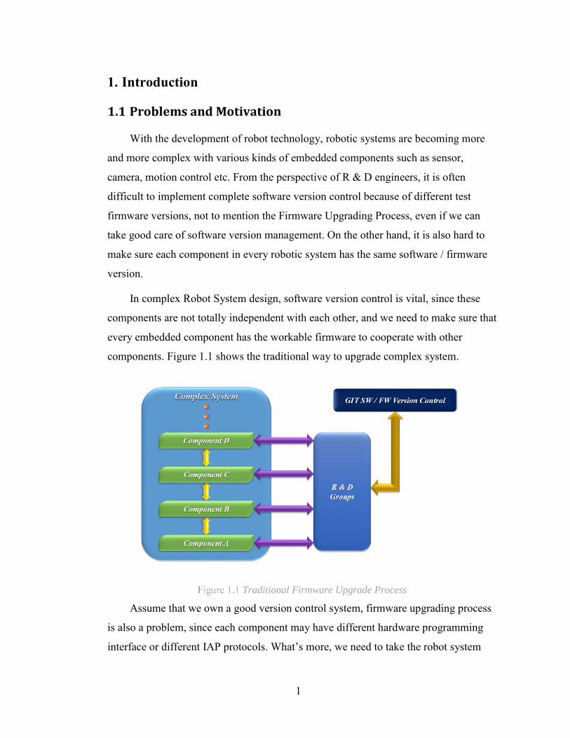
In complex Robot System design, software version control is vital, since these
components are not totally independent with each other, and we need to make sure that
every embedded component has the workable firmware to cooperate with other
components. Figure 1.1 shows the traditional way to upgrade complex system.
Traditional Firmware Upgrade Process
Assume that we own a good version control system, firmware upgrading process
is also a problem, since each component may have different hardware programming
interface or different IAP protocols. What’s more, we need to take the robot system

2
apart in order to upgrade some internal “tiny” modules which is definitely suffering
for engineers.
Note that all components are connected with each other via serial ports (USART /
SPI / I2C / USB etc.), we can design a cost-effective device connected to all modules
inside the robotic system which is only responsible for firmware upgrading, and once
the upgrading task finishes, it can be removed as if it never exists. From Figure 1.2 we
can see that the upgrader totally remove human factors from the Firmware Upgrade
process. In this way, a convenient and safe firmware upgrade process can be
guaranteed.
Block Diagram of Firmware Upgrader Application System
1.2 IAP Technology
In Application Programming (IAP) is widely applied in embedded systems. The
rationale of IAP is pretty simple. However, it needs hardware support (allow self-
programming, allow users to change the program counter any time). Currently, most
intelligent devices support IAP with extra support such as independent bootloader
flash section, software reset function etc. The IAP rationale is be shown in Figure 1.3.
Normally, MCUs execute the program in application region, when it receives an
upgrade request message from HOST (upgrader), it will clean internal registers and
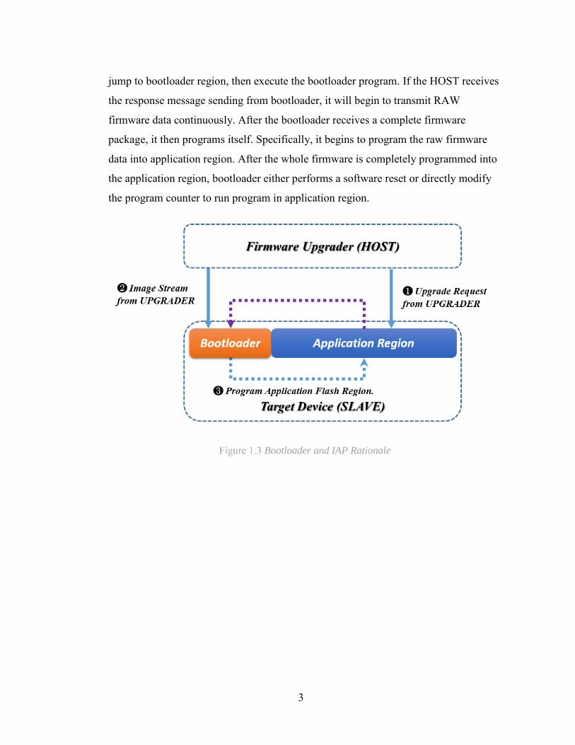
3
jump to bootloader region, then execute the bootloader program. If the HOST receives
the response message sending from bootloader, it will begin to transmit RAW
firmware data continuously. After the bootloader receives a complete firmware
package, it then programs itself. Specifically, it begins to program the raw firmware
data into application region. After the whole firmware is completely programmed into
the application region, bootloader either performs a software reset or directly modify
the program counter to run program in application region.
Bootloader and IAP Rationale
4
2. Design and Implementation
The system design involves in hardware design (hardware platform selection,
hardware interface level conversion) and software design (including communication
protocol design, master firmware design, slave bootloader design and simple GUI
design). After the hardware platform is selected, the first step is to design the
communication protocol, and then use the simplest hardware interface to verify its
basic functionality. Then the bootloader for AVR is designed to quickly check the
stability of communication. The final step is to finalize the protocol and exploit high
speed data transmission via DMA.
2.1 Hardware Design
The hardware design includes core MCU selection and interface level conversion
circuit design. Note that in this project, to save time, a development board is used to
implement the firmware upgrader, but it can definitely re-designed in the future to
reduce cost and size.
2.1.1 Hardware Platform Selection
The hardware of this firmware upgrader should own many common
communication interface, meanwhile, it must own fast storage interface such as SDIO,
USB HOST. In this case, the storage media will be SDHC / TF card since it is very
common, and can be embedded on-board. A good product should put user experience
as the most important factor, even though it may be tough for hardware and firmware
design.
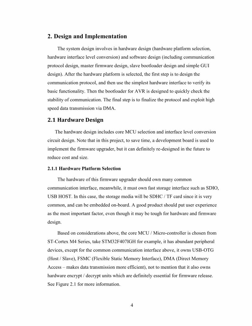
Based on considerations above, the core MCU / Micro-controller is chosen from
ST-Cortex M4 Series, take STM32F407IGH for example, it has abundant peripheral
devices, except for the common communication interface above, it owns USB-OTG
(Host / Slave), FSMC (Flexible Static Memory Interface), DMA (Direct Memory
Access – makes data transmission more efficient), not to mention that it also owns
hardware encrypt / decrypt units which are definitely essential for firmware release.
See Figure 2.1 for more information.
5
Note that, Ethernet is not a common firmware upgrade interface, furthermore, the
Ethernet physical chip is large and expensive. From the “Cost-Effective” purpose, it is
excluded from the block diagram, but it can be added at any time since STM32F4
itself owns hardware Ethernet even though it needs external PHY.
Hardware Block Diagram
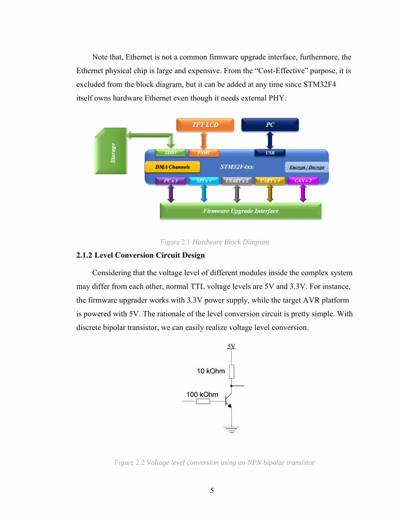
2.1.2 Level Conversion Circuit Design
Considering that the voltage level of different modules inside the complex system
may differ from each other, normal TTL voltage levels are 5V and 3.3V. For instance,
the firmware upgrader works with 3.3V power supply, while the target AVR platform
is powered with 5V. The rationale of the level conversion circuit is pretty simple. With
discrete bipolar transistor, we can easily realize voltage level conversion.
Voltage level conversion using an NPN bipolar transistor

6
Figure 2.2 can convert a voltage swing of 0-3V to a voltage swing of 0-5V. This
method was applied earlier in this project since it is very simple. Note that the pull-up
resistor value will affect the switching speed. The defect of this circuit is that it can
only perform unidirectional level conversion. To solve this problem, MOS-FETs with
backward diode between D and G was implemented to realize voltage level shift. This
level shifter (Figure 2.3) is also widely applied in I2C circuit to realize voltage
conversion.
Bi-directional level shifter [7]
2.2 Software Design
As mentioned in previous section, the software design contains communication
protocol design (SMARTLINK Protocol), master upgrader firmware design and slave
bootloader design. This section will merge design and software evaluation (if exists
any) together to describe each software part in detail.
2.2.1 Smart Link Protocol Design
The communication protocol should be able to perform basic master and slave
messages (functionalities) described below:
Request / Response firmware upgrade
This message is used to check device connection or device status, when slave
receive this message, it should response to master based on specific command.

7
Request / Response firmware transmission
This message tells slave device that the firmware data is about to transmit, when
slave receives this message, it should respond with the maximum firmware
segment size (internal RAM size) it supports.
Request / Response firmware raw data transmission
Master send this message to inform slave device to prepare to receive firmware
data. After slave successfully receives the data and program the firmware data
into flash, it should response to the master to report the programming results.
Note that the difference between Master and Slave is not absolute. If module B is
connected to the upgrader indirectly via Module A, then Module A should be able to
perform all master functionalities to Module B in order to perform indirect firmware
upgrade.
Now that all the basic functionalities are defined, the protocol package format
must be carefully designed to meet encryption and package checksum requirements.
Also, it must be able to be applied in either Peer-to-Peer or Bus connection. The
package anatomy is shown in Figure 2.4 and Figure 2.5.
Protocol Version – A (BUS)
Protocol Version – B (P2P)
Protocol Version A is suitable for those interfaces which support “Multi-Host”
and the low-layer protocol itself can distinguish different communication peers. For
instance, CAN low-layer protocol contains “Arbitration Field” which is composed of
“Identifier” and “RTR (Remote Transmission Request) bit”. With this field, we can
easily identifier the message sender even though this field is actually used for
communication arbitration (CAN Specification 2.0B).

8
Compared to protocol version A, version B is kind of verbose. However, this
kind of protocol format is necessary for those “Peer-to-Peer” communication
interfaces. Furthermore, this protocol can be used for “Sub-Module” Firmware
Upgrade. For instance, if a module (module X) is impossible to be connected to the
external interface, but it communicates with one of the modules (module Y) that
connects to the upgrader. In this way, upgrader can send X firmware to Y, and Y
upgrades X indirectly.
Both Protocol A and Protocol B are implemented with CRC-8 / 16 checksum
filed to enhance the communication safety. What’s more, it is also designed for
software convenience: if the “Header CRC8” is wrong, the whole package can be
ignored.
After the package format and functionalities are defined. It must be verified to
make sure that all request / response message can be correctly generated. To achieve
this, a software Test-Bench based on Visual Studio VC++ is created to explicitly
verify Smart Link.
Test Outputs from VC Test Bench
9
Figure 2.6 shows the results of P2P message (Protocol Version B) validation, As
soon as it passed the validation, the next step is to utilize the Smart-Link: It must be
lightweight, be compatible to most popular C compilers and be efficient. To achieve
this, a “Header File Only” Smart Link is further designed to meet these requirements.
Specifically, inline functions are widely used in Smart Link. The purpose of inline
functions is to achieve the same performance as macro function, and it can also be
further utilized based on different C compilers. For instance, to avoid the compiler not
to inline the functions, some C compilers let users to use some special assignments to
force the function to be inlined (__attribute__( ( always_inline ) )). The core function that
will affect the protocol efficiency would be the function which is used to decode the
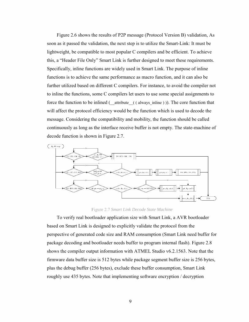
message. Considering the compatibility and mobility, the function should be called
continuously as long as the interface receive buffer is not empty. The state-machine of
decode function is shown in Figure 2.7.
Smart Link Decode State Machine
To verify real bootloader application size with Smart Link, a AVR bootloader
based on Smart Link is designed to explicitly validate the protocol from the
perspective of generated code size and RAM consumption (Smart Link need buffer for
package decoding and bootloader needs buffer to program internal flash). Figure 2.8
shows the compiler output information with ATMEL Studio v6.2.1563. Note that the
firmware data buffer size is 512 bytes while package segment buffer size is 256 bytes,
plus the debug buffer (256 bytes), exclude these buffer consumption, Smart Link
roughly use 435 bytes. Note that implementing software encryption / decryption
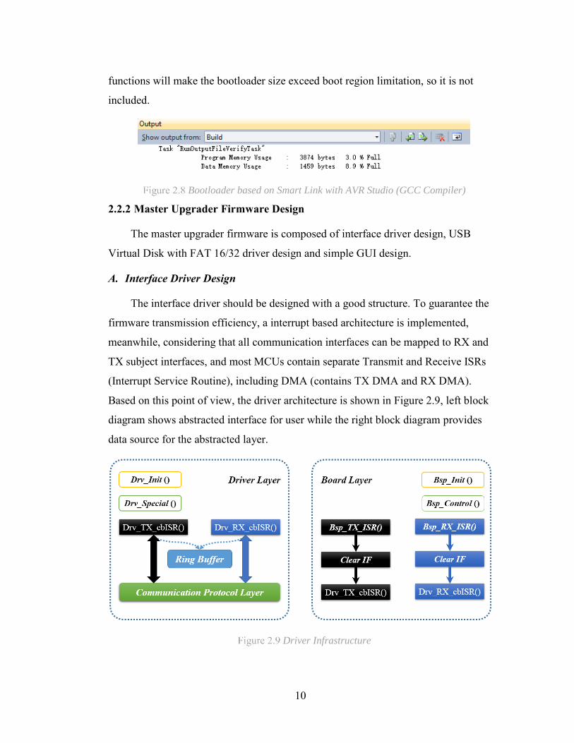
10
functions will make the bootloader size exceed boot region limitation, so it is not
included.
Bootloader based on Smart Link with AVR Studio (GCC Compiler)
2.2.2 Master Upgrader Firmware Design
The master upgrader firmware is composed of interface driver design, USB
Virtual Disk with FAT 16/32 driver design and simple GUI design.
A. Interface Driver Design
The interface driver should be designed with a good structure. To guarantee the
firmware transmission efficiency, a interrupt based architecture is implemented,
meanwhile, considering that all communication interfaces can be mapped to RX and
TX subject interfaces, and most MCUs contain separate Transmit and Receive ISRs
(Interrupt Service Routine), including DMA (contains TX DMA and RX DMA).
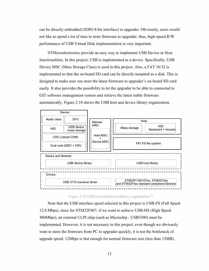
Based on this point of view, the driver architecture is shown in Figure 2.9, left block
diagram shows abstracted interface for user while the right block diagram provides
data source for the abstracted layer.
Driver Infrastructure

11
As shown in Figure 2.9, the driver layer and BSP (Board Support Package) layer
are clearly separated. All user functions are named as “Drv_xx_cbISR()” which
means it is a call-back function from low-layer ISR. Except for considerations above,
there still exists many notes for different interfaces.
SPI and USART are the most common communication interface. And the
DMA function is pretty easy to be implemented with buffer pointer and user
specified data length. For implementation purpose, all the hardware
addresses are defined in macro, which can be easily ported to any platform.
I2C is a well-known illness for STMicroelectronics, and this “illness” started
from CM3 (famous STM32F103). Even though CM4 platform fixed this
problem, official I2C library (CPAL) is not so efficient for firmware
upgrading. In this project, I2C and DMA interrupt are combined together to
achieve high performance.
CAN is largely used in industrial embedded applications, plus, it supports
“Multi-Host”, thus, it is a very important firmware upgrade interface. In this
project, cooperated with PC-Client Software, user can freely assign CAN-ID
to the upgrader, target board components with CAN interface. It is very
flexible and stable due to its robust low-layer communication protocol.
USB and FSMC (Flexible Static Memory Controller) are two famous
interfaces in STM32F series, and these two interfaces are very important in
this project. USB is responsible for data transmission between PC client and
storage media while FSMC is responsible for fast display (TFT). USB
interface is assigned with DMA channels to ensure transmission speed (will
be further verified). FSMC has no DMA support, therefore, software
utilization (mainly on memory operation) is essential.
B. USB Virtual Disk with FAT 16/32 Driver Design
Considering the system integrity and user experience – user don’t need to pull the
SD card out of upgrader in order to store latest firmware, instead, just connect the
upgrader to PC, and drag raw firmware file into it! Furthermore, in the future, eMMC
12
can be directly embedded (SDIO 8-bit interface) to upgrader. Obviously, users would
not like to spend a lot of time to store firmware to upgrader, thus, high-speed R/W
performance of USB Virtual Disk implementation is very important.
STMicroelectronics provide an easy way to implement USB Device or Host
functionalities. In this project, USB is implemented as a device. Specifically, USB
Device MSC (Mass Storage Class) is used in this project. Also, a FAT 16/32 is
implemented so that the on-board SD card can be directly mounted as a disk. This is
designed to make user can store the latest firmware to upgrader’s on-board SD card
easily. It also provides the possibility to let the upgrader to be able to connected to
GIT software management system and retrieve the latest stable firmware
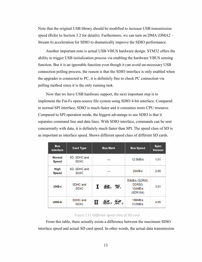
automatically. Figure 2.10 shows the USB host and device library organization.
USB host and device library organization[3]
Note that the USB interface speed selected in this project is USB-FS (Full Speed
12.0 Mbps), since for STM32F407, if we want to achieve USB-HS (High Speed
480Mbps), an external ULPI chip (such as Microchip - USB3300) must be
implemented. However, it is not necessary in this project, even though we obviously
want to store the firmware from PC to upgrader quickly, it is not the bottleneck of
upgrade speed. 12Mbps is fast enough for normal firmware size (less than 12MB).
13
Note that the original USB library should be modified to increase USB transmission
speed (Refer to Section 3.2 for details). Furthermore, we can turn on DMA (DMA2 –
Stream 6) acceleration for SDIO to dramatically improve the SDIO performance.
Another important note is actual USB-VBUS hardware design. STM32 offers the
ability to trigger USB initialization process via enabling the hardware VBUS sensing
function. But it is an ignorable function even though it can avoid un-necessary USB
connection polling process, the reason is that the SDIO interface is only enabled when
the upgrader is connected to PC, it is definitely fine to check PC connection via
polling method since it is the only running task.
Now that we have USB hardware support, the next important step is to
implement the Fat-Fs open-source file system using SDIO 4-bit interface. Compared
to normal SPI interface, SDIO is much faster and it consumes more CPU resource.
Compared to SPI operation mode, the biggest advantage to use SDIO is that it
separates command line and data lines. With SDIO interface, commands can be sent
concurrently with data, it is definitely much faster than SPI. The speed class of SD is
as important as interface speed. Shows different speed class of different SD cards.
Different speed class of SD card
From this table, there actually exists a difference between the maximum SDIO
interface speed and actual SD card speed. In other words, the actual data transmission

14
speed is limited by SDIO interface. Since the SDIO clock frequency of STM32F407 is
fixed at 48MHz, this means that SD card must support SDIO high speed (50MHz).
The SD card chosen in this project is manufactured by Kingston UHS-I SD card
(SDHC Class 4: speed > 4MB/s). Please note that the clock speed doesn’t stands for
actual data transmission speed, we can quickly forward the data stream via SDIO, but
SD card still need time to program the data stream into internal storage.
After the SDIO configuration, the next step is to implement low level SDIO
control with Fat-Fs hardware layer. The FatFs version used in this project is R0.10b.
It is fairly easy to transplant the Fat-Fs module, the only thing needs to do is change
the low layer file “diskio.h”, specifically, re-map the SD_disk_initialize(),
disk_initialize(), disk_read() and disk_write() functions to corresponding
STM32F4 SDIO functions. The mapping table is shown in Figure 2.12.
Fat-Fs Module Implementation
As soon as the Fat-Fs is implemented and SD card can be successfully initialized,
a speed test function is designed to explicitly validate the performance of SDIO 4-bit
mode when the upgrader is connected to PC. Figure 2.13 shows the SD card Read /
Write Speed Test results.

15
SDIO Read Write Speed Test
The result shown above is expected, the reason that write speed is much slower
than read is because Write operation requires file system to search free space to store
new data which consumes a lot of time. What’s more the write operation also needs to
read file allocation table, and perform verification process after the write operation is
over.
2.2.3 Slave Bootloader Design (AVR)
To verify the upgrader, a test bootloader must be designed. In this project, the
AVR board (ATmega16) used in ECE4760 to verify the basic functionalities of
firmware upgrader. This AVR bootloader is also a demonstration on how to use Smart
Link protocol.
To start with, the AVR bootloader region and size must be clarified. The flash
region allocation for ATmega1284p is shown in Figure 2.14.
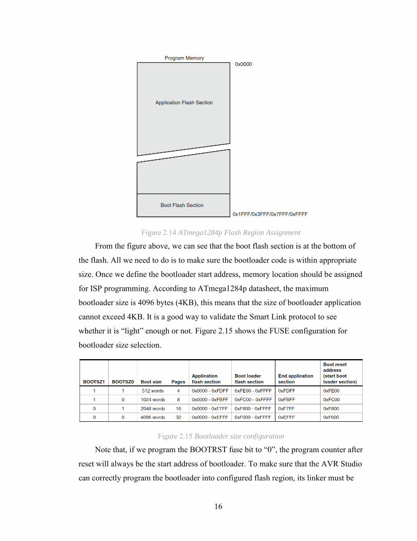
16
ATmega1284p Flash Region Assignment
From the figure above, we can see that the boot flash section is at the bottom of
the flash. All we need to do is to make sure the bootloader code is within appropriate
size. Once we define the bootloader start address, memory location should be assigned
for ISP programming. According to ATmega1284p datasheet, the maximum
bootloader size is 4096 bytes (4KB), this means that the size of bootloader application
cannot exceed 4KB. It is a good way to validate the Smart Link protocol to see
whether it is “light” enough or not. Figure 2.15 shows the FUSE configuration for
bootloader size selection.
Bootloader size configuration
Note that, if we program the BOOTRST fuse bit to “0”, the program counter after
reset will always be the start address of bootloader. To make sure that the AVR Studio
can correctly program the bootloader into configured flash region, its linker must be
17
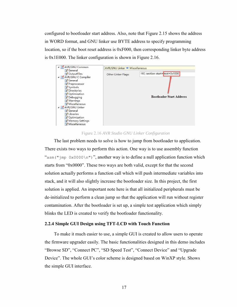
configured to bootloader start address. Also, note that Figure 2.15 shows the address
in WORD format, and GNU linker use BYTE address to specify programming
location, so if the boot reset address is 0xF000, then corresponding linker byte address
is 0x1E000. The linker configuration is shown in Figure 2.16.
AVR Studio GNU Linker Configuration
The last problem needs to solve is how to jump from bootloader to application.
There exists two ways to perform this action. One way is to use assembly function
“asm("jmp 0x0000\n")”, another way is to define a null application function which
starts from “0x0000”. These two ways are both valid, except for that the second
solution actually performs a function call which will push intermediate variables into
stack, and it will also slightly increase the bootloader size. In this project, the first
solution is applied. An important note here is that all initialized peripherals must be
de-initialized to perform a clean jump so that the application will run without register
contamination. After the bootloader is set up, a simple test application which simply
blinks the LED is created to verify the bootloader functionality.
2.2.4 Simple GUI Design using TFT-LCD with Touch Function
To make it much easier to use, a simple GUI is created to allow users to operate
the firmware upgrader easily. The basic functionalities designed in this demo includes
“Browse SD”, “Connect PC”, “SD Speed Test”, “Connect Device” and “Upgrade
Device”. The whole GUI’s color scheme is designed based on WinXP style. Shows
the simple GUI interface.
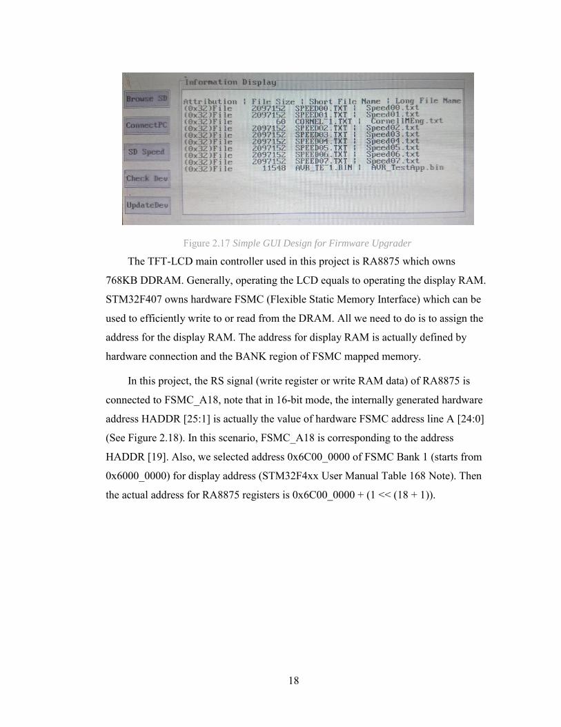
18
Simple GUI Design for Firmware Upgrader
The TFT-LCD main controller used in this project is RA8875 which owns
768KB DDRAM. Generally, operating the LCD equals to operating the display RAM.
STM32F407 owns hardware FSMC (Flexible Static Memory Interface) which can be
used to efficiently write to or read from the DRAM. All we need to do is to assign the
address for the display RAM. The address for display RAM is actually defined by
hardware connection and the BANK region of FSMC mapped memory.
In this project, the RS signal (write register or write RAM data) of RA8875 is
connected to FSMC_A18, note that in 16-bit mode, the internally generated hardware
address HADDR [25:1] is actually the value of hardware FSMC address line A [24:0]
(See Figure 2.18). In this scenario, FSMC_A18 is corresponding to the address
HADDR [19]. Also, we selected address 0x6C00_0000 of FSMC Bank 1 (starts from
0x6000_0000) for display address (STM32F4xx User Manual Table 168 Note). Then
the actual address for RA8875 registers is 0x6C00_0000 + (1 << (18 + 1)).

19
FSMC Bank Address Map
In actual programming, we can simply define the register / RAM RW operation
address shown in Figure 2.19.
RA8875 Address Definition
With this kind of definition, we can simply RW either RA8875’s RAM or
registers by simply reading or writing to corresponding address. There still exists so
many utilization that can be applied to efficiently operate the LCD, which will not be
further discussed due to document space limitation.

20
3. Testing and Results
To fully verify the whole system, appropriate testing is also very important. The
test includes: Internal SD card R/W Test, PC to upgrader R/W speed test, UART to
AVR firmware upgrading test and CAN to STM32 firmware upgrading test.
3.1 Internal SD card R/W Test
This test aims to validate both SDIO (4-bit mode) and Fat-FS performance. The
test program is designed to recursively write natural numbers to SD card by creating a
test text file (2MB), and then read it out. By using internal System Tick to count the
read, write time, RW speed can be explicitly calculated in a very accurate way. As
mentioned above, user can test SD card any time. Figure 3.1 shows the one of the
testing results.
SD Read Write Speed Test
Multiple tests are executed to fully validate the SD RW performance. The results is
shown in Figure 3.2.
Multiple Pressure Testing Results
Test # Read Speed (KB/s) Write Speed (KB/s)
0 4196 13561 4213 13912 4205 12703 4213 1396
Average 4206.75 1353.25

21
3.2 Firmware Transmission Speed (PC to Upgrader)
This test is an enhanced test that covers the test in previous section, plus the USB
transmission speed test. The firmware transmission speed can directly impact user
experience. The expected write and read speed should be lower than direct SDIO R/W
speed since USB is involved. In real test, the R / W speed is actually limited by the
FS-USB interface (12Mbps). Before doing this test, the SD card is formatted with
official formatting tool to guarantee the accuracy of testing results. The test includes
single file and scattered files R/W test with different size. The result is shown in
Figure 3.3.
Firmware Transmission Speed Test
Note that, the STM32 USB library is modified to achieve this performance, original
library can only achieve 33KB/s (EP-OUT: Master to Slave) performance. By
modifying the maximum transfer size from 64 to 65536 (Increase internal data buffer
size) and use PING-PONG buffer strategy to implement BULK transmission, the USB
transmission speed can be increased up to 1215 KB/s.
Read Speed (KB/s) Write Speed (KB/s) Read Speed (KB/s) Write Speed (KB/s)
512 KB 924 652 785 4501 MB 985 671 797 5022 MB 1017 695 812 5194 MB 1123 704 907 517
Single File Scattered Files (8 Files)Size

22
3.1 Interface Speed Test
This test aims to verify the firmware upgrading efficiency, in this test, USART,
USART with DMA and CAN interface are tested with different firmware size. Shows
the testing results.
Different Interface Speed Test
From the result above we can see that, DMA can indeed save time. If the receiver
(AVR Board) also support DMA, then the performance would definitely be better.
Note that STM32 USART can achieve 10.5Mbps transmission speed while the
maximum BAUD configuration for ATmega1284p is only 115200bps. From This
point of view, the firmware transmission speed is actually limited by target device.
This limitation can also be observed from the comparison of USART and CAN
(10Mbps). Note that, there also exists a factor that may affect transmission speed –
CRC8 / CRC16 package verification and decryption. If the target device has no
corresponding hardware units, then software solution must be applied, thus it will also
hurt firmware upgrade efficiency.
3 6 11.8 24.7UART 275 600.5 1265.74 2450.82UART-DMA 272.37 593.42 1234.28 2395.82CAN 30.62 79.612 131.675 275.392
0
500
1000
1500
2000
2500
3000
Upg
rade
Tim
e (m
s)
Interface Speed Test
UART UART-DMA CAN

23
4. Conclusions
In this project, an efficient firmware upgrader was designed and could perform
firmware upgrade to target device based on IAP methodology. Multiple interface
drivers are designed to verify system efficiency. From this project, I learned that a
good embedded system is not only composed of high-quality hardware, firmware
design is also important. Good firmware design sometimes can make up hardware
defects while slight hardware modifications can make the software design easier. For
embedded system design, both hardware and software are scalable. Even though this
system can perform required standard firmware upgrade process, it still exists some
defects and so much space for further modifications and improvements.
4.1 Future Work
Currently, when multiple device are connected to this system, it can only perform
firmware upgrade process in order. However, it is possible to upgrade all connected
systems simultaneously using interrupt-based data transmission strategy. Once the
protocol version, target device ID and firmware segment size is identified, firmware
data transmission can be automatically triggered by interface transmission interrupt.
However, with this kind of architecture, the software design will become much more
complicate since there exists multiple interrupt service routine to be handled, and
current Smart-Link may need to be modified to cooperate with this kind of design.
As mentioned in the abstract, a PC Client application can be designed to achieve
“Hardware Customization”, user can define system module inter-connection, interface
type and more important, automatically fetch the latest, stable firmware from GIT
software management system. It indeed needs to be carefully designed to make the
upgrader much more easy to use.
Another improvement is upgrader’s own GUI design. Current project
implemented a TFT-LCD to improve user experience, it can be replaced with small
OLED module and simple buttons.

24
5. Acknowledgements
I would like to thank my advisor – Professor Bruce Land for his trust and
encouragement. His trust always give me power to overcome one difficulty after
another, also, he gave me so many valuable suggestions that make this project much
easier to finish. I also learned a lot from his class, his bottomless knowledge always
brings me to an unknown field. I feel so lucky to be one of his students.
I also want to thank Cornell ECE for providing me with such a great place to
learn, share and move forward. Learning in Cornell would be an indelible experience
for me. Sincere thanks to all my professors and excellent classmates.

25
6. Reference
[1]. STMicroelectronics. STM32F4 Series User Manual Rev 2, http://www.st.com;
[2]. STMicroelectronics. “Production programming solutions for the STM32”;
[3]. STMicroelectronics. “USB On-The-Go host and device library User Manual”;
[4]. RA8875 Character / Graphic TFT LCD Controller Specification;
[5]. SD Group, and SD Card Association. "SD Specifications Part 1 Physical Layer
Specification";
[6]. SD Group, and SD Card Association. "SD Specifications Part E1 SDIO
Specification";
[7]. NXP Semiconductors. “Level shifting techniques in I2C-bus design” “v.01”;
[8]. Specification, Universal Serial Bus. "Rev. 2.0." ARM, http://www.arm.com
(2000).
[9]. FatFs Module Specification, http://elm-chan.org;
[10]. Specification, C. A. N. "v2. 0." Common Public Radio Interface (CPRI)
(2004): 1-75.
26
7. Appendix
Smart Link (Draft Version)
#ifndef _SMARTLINK_H_ #define _SMARTLINK_H_ /** ****************************************************************************** * @file smartlink.h * @author Wancheng Zhou * @version beta * @date 08-November-2014 * @brief This file provides firmware functions to manage the following * functionalities of Firmware Upgrader. * + Package Request Message from Master * + Package Response Message to Slave * + Decode Firmware Upgrade Message * * @verbatim * ****************************************************************************** **/ /* Includes ------------------------------------------------------------------*/ #include <stdint.h> #include "crc_check.h" #ifdef __cplusplus extern "C" { #endif /* * SMTLINK Protocol Definition * * P2P Interface Protocol (Such as USART / SPI etc.) * ___________________________________________________________________________ * | SOF | VERLEN | HDRCRC8 | SND | RCV | SEQ | CMDTP | CMDID | DAT | PKGCRC16 | * |__1__|____2___|____1____|__1__|__1__|__2__|___1___|___1___|__n__|____2_____| * * Message Length (Byte): 12 + n * * BUS Interface Protocol (Such as CAN)

27
* _________________________________________________ * | SOF | VERLEN | HDRCRC8 | CMDID | DAT | PKGCRC16 | * |__1__|____2___|____1____|___1___|__n__|____2_____| * * Message Length (Byte): 7 + n */ /* Private define ------------------------------------------------------------*/ #define SMTLINK_HOST_ID 0xE5 #define SMTLINK_CRC8_KEY 0xFE #define SMTLINK_CRC16_KEY 0xFEFE #define SMTLINK_STX 0x55 #define SMTLINK_STX_LOC 0 #define SMTLINK_VER_LEN_LOC 1 #define SMTLINK_VER_WIDTH 6 /*!> Version: 6-Bit */ #define SMTLINK_LEN_WIDTH 10 /*!> Length: 10-Bit */ #define SMTLINK_GET_VER(dat) (dat & 0xFC00) >> 10 /*!> "dat" is 16-Bit VERLEN region */ #define SMTLINK_GET_LEN(dat) (dat & 0x03FF) /*!> "dat" is 16-Bit VERLEN region */ #define SMTLINK_HDR_CRC8_LOC 3 #define SMTLINK_SNDR_LOC 4 #define SMTLINK_RCVR_LOC 5 #define SMTLINK_SEQ_NUM_LOC 6 #define SMTLINK_CMD_TP_LOC 8 #define SMTLINK_P2P_CMD_ID_LOC 9 #define SMTLINK_BUS_CMD_ID_LOC 4 #define SMTLINK_P2P_DAT_START_LOC 10 #define SMTLINK_BUS_DAT_START_LOC (SMTLINK_P2P_DAT_START_LOC - 5) #define SMTLINK_P2P_FWUPDREQMSG_LEN 21 #define SMTLINK_BUS_FWUPDREQMSG_LEN (SMTLINK_P2P_FWUPDREQMSG_LEN - 5) #define SMTLINK_P2P_FWUPDRESPMSG_LEN 13 #define SMTLINK_BUS_FWUPDRESPMSG_LEN (SMTLINK_P2P_FWUPDRESPMSG_LEN - 5) #define SMTLINK_P2P_FWRCVREQMSG_LEN 25 #define SMTLINK_BUS_FWRCVREQMSG_LEN (SMTLINK_P2P_FWRCVREQMSG_LEN - 5) #define SMTLINK_P2P_FWRCVRESPMSG_LEN 15 #define SMTLINK_BUS_FWRCVRESPMSG_LEN (SMTLINK_P2P_FWRCVRESPMSG_LEN - 5) #define SMTLINK_P2P_FWDAT_START_LOC (SMTLINK_P2P_DAT_START_LOC + 7) #define SMTLINK_BUS_FWDAT_START_LOC (SMTLINK_BUS_DAT_START_LOC + 7) #define SMTLINK_P2P_FWTXREQMSG_LEN(segsz) (12 + 7 + segsz) #define SMTLINK_P2P_FWTXRESPMSG_LEN 13 #define SMTLINK_BUS_FWTXREQMSG_LEN(segsz)
28
#define SMTLINK_P2P_FWDAT_START_LOC (SMTLINK_P2P_DAT_START_LOC + 7) #define SMTLINK_BUS_FWDAT_START_LOC (SMTLINK_BUS_DAT_START_LOC + 7) #define SMTLINK_P2P_FWTXREQMSG_LEN(segsz) (12 + 7 + segsz) #define SMTLINK_P2P_FWTXRESPMSG_LEN 13 #define SMTLINK_BUS_FWTXREQMSG_LEN(segsz) SMTLINK_P2P_FWTXREQMSG_LEN(segsz) - 5 #define SMTLINK_BUS_FWTXRESPMSG_LEN SMTLINK_P2P_FWTXRESPMSG_LEN - 5 typedef enum { SMTLINK_BUS_VER = (0), SMTLINK_P2P_VER = (1), SMTLINK_ERR_VER = (3) } SMT_Ver_TypeDef; typedef enum { SMTLINK_CMD_REQ_FW_UPD = (0), SMTLINK_CMD_REQ_FW_DAT = (1), SMTLINK_CMD_TX_FW_DAT = (2), SMTLINK_CMD_TX_FW_DONE = (3) } SMT_CmdID_TypeDef; typedef enum { FW_UPD_CHECK_STX = (0), FW_UPD_CHECK_HDR_CRC = (1), FW_UPD_CHECK_PKG_CRC = (2) } FW_PkgCheck_TypeDef; typedef enum { SMTLINK_PKG_TP_REQ = (0), SMTLINK_PKG_TP_RESP = (1) } SMT_Pkg_TypeDef; typedef enum { SMTLINK_PKG_NO_ACK = (0), SMTLINK_PKG_NEED_ACK = (1) } SMT_PkgAck_TypeDef; typedef struct { SMT_Ver_TypeDef pkg_ver; uint8_t sender; SMT_CmdID_TypeDef cmd_id; } SMTLINK_MsgInfo_TypeDef; __inline SMT_Ver_TypeDef SMTLINK_GetPkgVer(uint16_t pkg_verlen) { return (SMT_Ver_TypeDef)((pkg_verlen & 0xFC00) >> 10); } __inline uint16_t SMTLINK_GetPkgLen(uint16_t pkg_verlen) { return (pkg_verlen & 0x03FF); }

29
__inline uint16_t SMTLINK_PackVerLen(SMT_Ver_TypeDef version, uint16_t len) { return (uint16_t)(((version & 0x1F) << 10) | (len & 0x3FF)); } __inline SMT_Pkg_TypeDef SMTLINK_GetPkgType(uint8_t cmd_tp) { return (SMT_Pkg_TypeDef)(cmd_tp & (1 << 7)); } __inline SMT_PkgAck_TypeDef SMTLINK_GetPkgAckType(uint8_t cmd_tp) { return (SMT_PkgAck_TypeDef)(cmd_tp & (1 << 6)); } __inline uint8_t SMTLINK_PackPkgAckTp(SMT_Pkg_TypeDef pkg_tp, SMT_PkgAck_TypeDef ack_tp) { return (uint8_t)((pkg_tp << 7) | (ack_tp << 5)); } __inline void SMTLINK_PackMsgHead( SMT_Ver_TypeDef smt_ver, SMT_Pkg_TypeDef pkg_tp, SMT_PkgAck_TypeDef ack_tp, SMT_CmdID_TypeDef cmd_id, uint8_t sdr_id, uint8_t rcv_id, uint8_t *msg_buff, uint16_t msg_len) { uint16_t pkg_verlen; uint8_t pkg_ack_tp; uint16_t pkg_seqnum; uint8_t cmd_id_loc; pkg_verlen = SMTLINK_PackVerLen (SMTLINK_P2P_VER, msg_len); pkg_ack_tp = SMTLINK_PackPkgAckTp (pkg_tp, ack_tp); /* Request Package, Need ACK */ cmd_id_loc = (smt_ver == SMTLINK_P2P_VER) ? (SMTLINK_P2P_CMD_ID_LOC) : (SMTLINK_BUS_CMD_ID_LOC); pkg_seqnum = 0x0000; msg_buff[SMTLINK_STX_LOC] = SMTLINK_STX; *(uint16_t*)(&msg_buff[SMTLINK_VER_LEN_LOC]) = pkg_verlen; msg_buff[SMTLINK_HDR_CRC8_LOC] = crc8_update(SMTLINK_CRC8_KEY, msg_buff, 3); if (smt_ver == SMTLINK_P2P_VER) { msg_buff[SMTLINK_SNDR_LOC] = sdr_id; msg_buff[SMTLINK_RCVR_LOC] = rcv_id; msg_buff[SMTLINK_SEQ_NUM_LOC] = (pkg_seqnum & 0xFF00) >> 8; msg_buff[SMTLINK_SEQ_NUM_LOC + 1] = pkg_seqnum & 0x00FF; msg_buff[SMTLINK_CMD_TP_LOC] = pkg_ack_tp; } msg_buff[cmd_id_loc] = cmd_id;
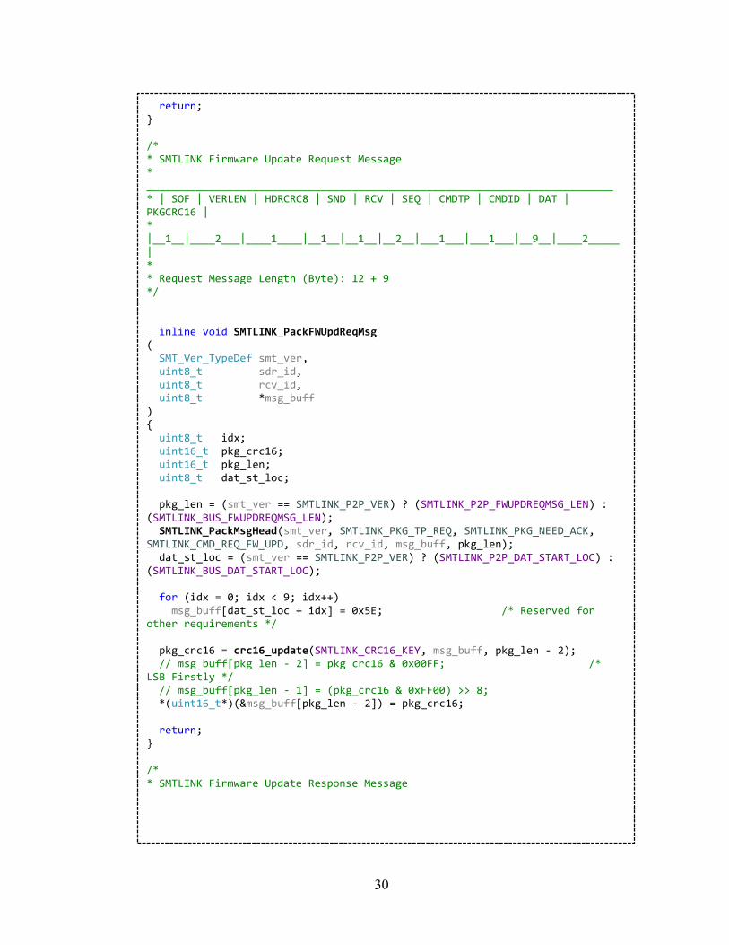
30
return; } /* * SMTLINK Firmware Update Request Message * ___________________________________________________________________________ * | SOF | VERLEN | HDRCRC8 | SND | RCV | SEQ | CMDTP | CMDID | DAT | PKGCRC16 | * |__1__|____2___|____1____|__1__|__1__|__2__|___1___|___1___|__9__|____2_____| * * Request Message Length (Byte): 12 + 9 */ __inline void SMTLINK_PackFWUpdReqMsg ( SMT_Ver_TypeDef smt_ver, uint8_t sdr_id, uint8_t rcv_id, uint8_t *msg_buff ) { uint8_t idx; uint16_t pkg_crc16; uint16_t pkg_len; uint8_t dat_st_loc; pkg_len = (smt_ver == SMTLINK_P2P_VER) ? (SMTLINK_P2P_FWUPDREQMSG_LEN) : (SMTLINK_BUS_FWUPDREQMSG_LEN); SMTLINK_PackMsgHead(smt_ver, SMTLINK_PKG_TP_REQ, SMTLINK_PKG_NEED_ACK, SMTLINK_CMD_REQ_FW_UPD, sdr_id, rcv_id, msg_buff, pkg_len); dat_st_loc = (smt_ver == SMTLINK_P2P_VER) ? (SMTLINK_P2P_DAT_START_LOC) : (SMTLINK_BUS_DAT_START_LOC); for (idx = 0; idx < 9; idx++) msg_buff[dat_st_loc + idx] = 0x5E; /* Reserved for other requirements */ pkg_crc16 = crc16_update(SMTLINK_CRC16_KEY, msg_buff, pkg_len - 2); // msg_buff[pkg_len - 2] = pkg_crc16 & 0x00FF; /* LSB Firstly */ // msg_buff[pkg_len - 1] = (pkg_crc16 & 0xFF00) >> 8; *(uint16_t*)(&msg_buff[pkg_len - 2]) = pkg_crc16; return; } /* * SMTLINK Firmware Update Response Message
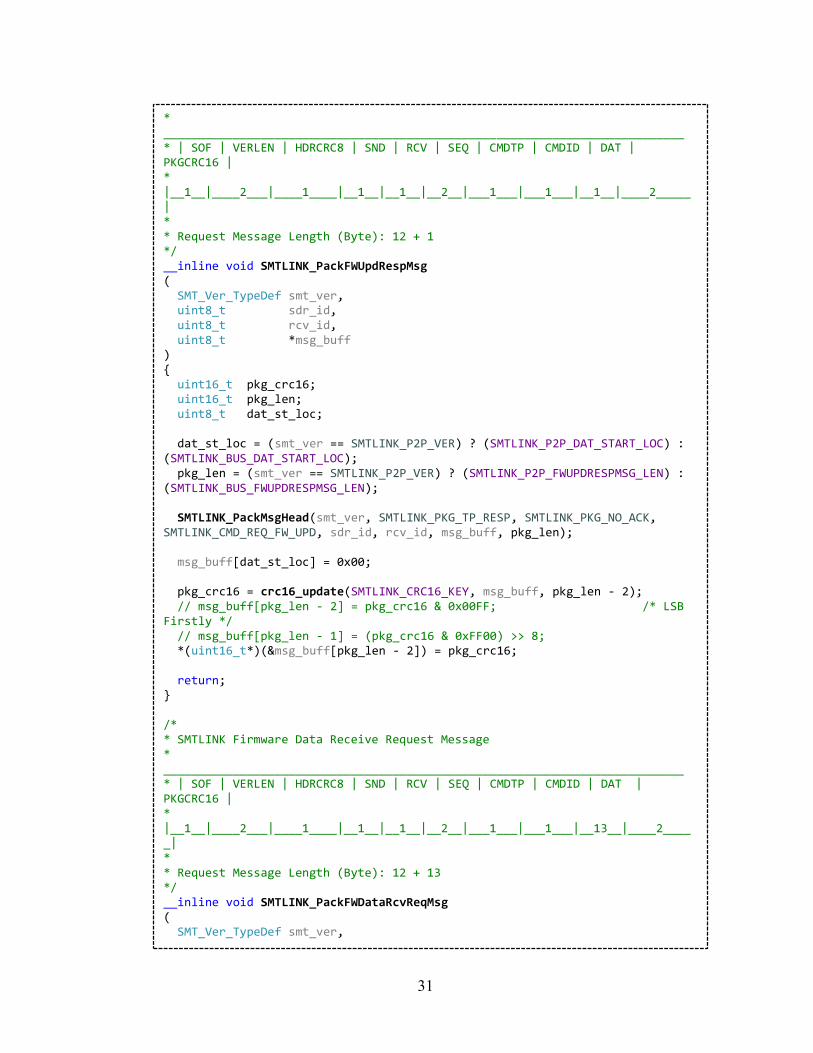
31
* ___________________________________________________________________________ * | SOF | VERLEN | HDRCRC8 | SND | RCV | SEQ | CMDTP | CMDID | DAT | PKGCRC16 | * |__1__|____2___|____1____|__1__|__1__|__2__|___1___|___1___|__1__|____2_____| * * Request Message Length (Byte): 12 + 1 */ __inline void SMTLINK_PackFWUpdRespMsg ( SMT_Ver_TypeDef smt_ver, uint8_t sdr_id, uint8_t rcv_id, uint8_t *msg_buff ) { uint16_t pkg_crc16; uint16_t pkg_len; uint8_t dat_st_loc; dat_st_loc = (smt_ver == SMTLINK_P2P_VER) ? (SMTLINK_P2P_DAT_START_LOC) : (SMTLINK_BUS_DAT_START_LOC); pkg_len = (smt_ver == SMTLINK_P2P_VER) ? (SMTLINK_P2P_FWUPDRESPMSG_LEN) : (SMTLINK_BUS_FWUPDRESPMSG_LEN); SMTLINK_PackMsgHead(smt_ver, SMTLINK_PKG_TP_RESP, SMTLINK_PKG_NO_ACK, SMTLINK_CMD_REQ_FW_UPD, sdr_id, rcv_id, msg_buff, pkg_len); msg_buff[dat_st_loc] = 0x00; pkg_crc16 = crc16_update(SMTLINK_CRC16_KEY, msg_buff, pkg_len - 2); // msg_buff[pkg_len - 2] = pkg_crc16 & 0x00FF; /* LSB Firstly */ // msg_buff[pkg_len - 1] = (pkg_crc16 & 0xFF00) >> 8; *(uint16_t*)(&msg_buff[pkg_len - 2]) = pkg_crc16; return; } /* * SMTLINK Firmware Data Receive Request Message * ___________________________________________________________________________ * | SOF | VERLEN | HDRCRC8 | SND | RCV | SEQ | CMDTP | CMDID | DAT | PKGCRC16 | * |__1__|____2___|____1____|__1__|__1__|__2__|___1___|___1___|__13__|____2_____| * * Request Message Length (Byte): 12 + 13 */ __inline void SMTLINK_PackFWDataRcvReqMsg ( SMT_Ver_TypeDef smt_ver,

32
uint8_t sdr_id, uint8_t rcv_id, uint32_t fw_size, uint8_t *msg_buff ) { uint8_t idx; uint16_t pkg_crc16; uint16_t pkg_len; uint8_t dat_st_loc; dat_st_loc = (smt_ver == SMTLINK_P2P_VER) ? (SMTLINK_P2P_DAT_START_LOC) : (SMTLINK_BUS_DAT_START_LOC); pkg_len = (smt_ver == SMTLINK_P2P_VER) ? (SMTLINK_P2P_FWRCVREQMSG_LEN) : (SMTLINK_BUS_FWRCVREQMSG_LEN); SMTLINK_PackMsgHead(smt_ver, SMTLINK_PKG_TP_REQ, SMTLINK_PKG_NEED_ACK, SMTLINK_CMD_REQ_FW_DAT, sdr_id, rcv_id, msg_buff, pkg_len); msg_buff[dat_st_loc] = 0x00; /* DAT[0] is reserved for encryption type */ *(uint32_t*)(&msg_buff[dat_st_loc + 1]) = fw_size; /* DAT[1] - DAT[4] is firmware size */ for (idx = 0; idx < 8; idx++) /* DAT[5] - DAT[12] reserved */ msg_buff[dat_st_loc + 5 + idx] = 0x00; /* Handshake validation for further extension */ pkg_crc16 = crc16_update(SMTLINK_CRC16_KEY, msg_buff, pkg_len - 2); *(uint16_t*)(&msg_buff[pkg_len - 2]) = pkg_crc16; return; } /** * SMTLINK Firmware Data Receive Response Message * ___________________________________________________________________________ * | SOF | VERLEN | HDRCRC8 | SND | RCV | SEQ | CMDTP | CMDID | DAT | PKGCRC16 | * |__1__|____2___|____1____|__1__|__1__|__2__|___1___|___1___|__3__|____2_____| * * Request Message Length (Byte): 12 + 3 */ __inline void SMTLINK_PackFWDataRcvRespMsg ( SMT_Ver_TypeDef smt_ver, uint8_t sdr_id, uint8_t rcv_id, uint16_t fw_seg_size, uint8_t *msg_buff )

33
{ uint16_t pkg_crc16; uint16_t pkg_len; uint8_t dat_st_loc; dat_st_loc = (smt_ver == SMTLINK_P2P_VER) ? (SMTLINK_P2P_DAT_START_LOC) : (SMTLINK_BUS_DAT_START_LOC); pkg_len = (smt_ver == SMTLINK_P2P_VER) ? (SMTLINK_P2P_FWRCVRESPMSG_LEN) : (SMTLINK_BUS_FWRCVRESPMSG_LEN); SMTLINK_PackMsgHead(smt_ver, SMTLINK_PKG_TP_RESP, SMTLINK_PKG_NO_ACK, SMTLINK_CMD_REQ_FW_DAT, sdr_id, rcv_id, msg_buff, pkg_len); msg_buff[dat_st_loc] = 0x00; *(uint16_t*)(&msg_buff[dat_st_loc + 1]) = fw_seg_size; pkg_crc16 = crc16_update(SMTLINK_CRC16_KEY, msg_buff, pkg_len - 2); *(uint16_t*)(&msg_buff[pkg_len - 2]) = pkg_crc16; return; } __inline uint16_t SMTLINK_GetFWData_SegmentSize(SMT_Ver_TypeDef smt_ver, uint8_t *msg_buff) { uint8_t dat_st_loc; uint16_t fw_seg_size; dat_st_loc = (smt_ver == SMTLINK_P2P_VER) ? (SMTLINK_P2P_DAT_START_LOC) : (SMTLINK_BUS_DAT_START_LOC); fw_seg_size = *(uint16_t*)(&msg_buff[dat_st_loc + 1]); return fw_seg_size; } /** * SMTLINK Firmware Data Transmit Request Message * ___________________________________________________________________________ * | SOF | VERLEN | HDRCRC8 | SND | RCV | SEQ | CMDTP | CMDID | DAT | PKGCRC16 | * |__1__|____2___|____1____|__1__|__1__|__2__|___1___|___1___|__n__|____2_____| * * Request Message Length (Byte): 12 + n (n = 7 + fw_seg_size) * * NOTE: Prepare firmware data before calling this function and make sure the * buffer size is sufficient. */ __inline void SMTLINK_PackFWDataTXReqMsg ( SMT_Ver_TypeDef smt_ver, uint8_t sdr_id, uint8_t rcv_id, uint16_t fw_seq_num,

34
uint16_t fw_seg_size, uint8_t *msg_buff ) { uint16_t pkg_crc16; uint16_t pkg_len; uint8_t dat_st_loc; dat_st_loc = (smt_ver == SMTLINK_P2P_VER) ? (SMTLINK_P2P_DAT_START_LOC) : (SMTLINK_BUS_DAT_START_LOC); pkg_len = (smt_ver == SMTLINK_P2P_VER) ? (SMTLINK_P2P_FWTXREQMSG_LEN(fw_seg_size)) : (SMTLINK_BUS_FWTXREQMSG_LEN(fw_seg_size)); SMTLINK_PackMsgHead(smt_ver, SMTLINK_PKG_TP_REQ, SMTLINK_PKG_NEED_ACK, SMTLINK_CMD_TX_FW_DAT, sdr_id, rcv_id, msg_buff, pkg_len); msg_buff[dat_st_loc] = 0x00; *(uint32_t*)(&msg_buff[dat_st_loc + 1]) = fw_seq_num; *(uint16_t*)(&msg_buff[dat_st_loc + 5]) = fw_seg_size; pkg_crc16 = crc16_update(SMTLINK_CRC16_KEY, msg_buff, pkg_len - 2); *(uint16_t*)(&msg_buff[pkg_len - 2]) = pkg_crc16; return; } __inline void SMTLINK_PackFWData_StuffBuff ( SMT_Ver_TypeDef smt_ver, uint8_t *msg_buff, uint8_t *data_pool, uint16_t fw_seg_size ) { uint16_t idx; uint8_t fw_dat_st_loc; fw_dat_st_loc = (smt_ver == SMTLINK_P2P_VER) ? (SMTLINK_P2P_DAT_START_LOC + 7) : (SMTLINK_BUS_DAT_START_LOC + 7); for (idx = 0; idx < fw_seg_size; idx++) { msg_buff[fw_dat_st_loc + idx] = data_pool[idx]; } return; }
/** * SMTLINK Firmware Data Transmit Response Message * ___________________________________________________________________________ * | SOF | VERLEN | HDRCRC8 | SND | RCV | SEQ | CMDTP | CMDID | DAT | PKGCRC16 | * |__1__|____2___|____1____|__1__|__1__|__2__|___1___|___1___|__1__|____2_____| *

35
* Request Message Length (Byte): 12 + 1 * * NOTE: Prepare firmware data before calling this function and make sure the * buffer size is sufficient. */ __inline void SMTLINK_PackFWDataTXRespMsg ( SMT_Ver_TypeDef smt_ver, uint8_t sdr_id, uint8_t rcv_id, uint8_t *msg_buff ) { uint16_t pkg_crc16; uint16_t pkg_len; uint8_t dat_st_loc; dat_st_loc = (smt_ver == SMTLINK_P2P_VER) ? (SMTLINK_P2P_DAT_START_LOC) : (SMTLINK_BUS_DAT_START_LOC); pkg_len = (smt_ver == SMTLINK_P2P_VER) ? (12 + 1) : (7 + 1); SMTLINK_PackMsgHead(smt_ver, SMTLINK_PKG_TP_RESP, SMTLINK_PKG_NO_ACK, SMTLINK_CMD_TX_FW_DAT, sdr_id, rcv_id, msg_buff, pkg_len); msg_buff[dat_st_loc] = 0x00; pkg_crc16 = crc16_update(SMTLINK_CRC16_KEY, msg_buff, pkg_len - 2); *(uint16_t*)(&msg_buff[pkg_len - 2]) = pkg_crc16; return; }
__inline bool SMTLINK_UnPackMsg ( uint8_t rcv_dat, uint8_t *msg_buff, uint16_t *buff_ptr, SMTLINK_MsgInfo_TypeDef *msg_info ) { static uint16_t pkg_len; static SMT_Ver_TypeDef pkg_ver; static FW_PkgCheck_TypeDef pkg_chk_stage = FW_UPD_CHECK_STX;
bool check_reslt = false; uint16_t pkg_verlen; uint16_t pkg_crc16;
switch (pkg_chk_stage) { case FW_UPD_CHECK_STX: if (rcv_dat == SMTLINK_STX) pkg_chk_stage = FW_UPD_CHECK_HDR_CRC; else *buff_ptr = 0;
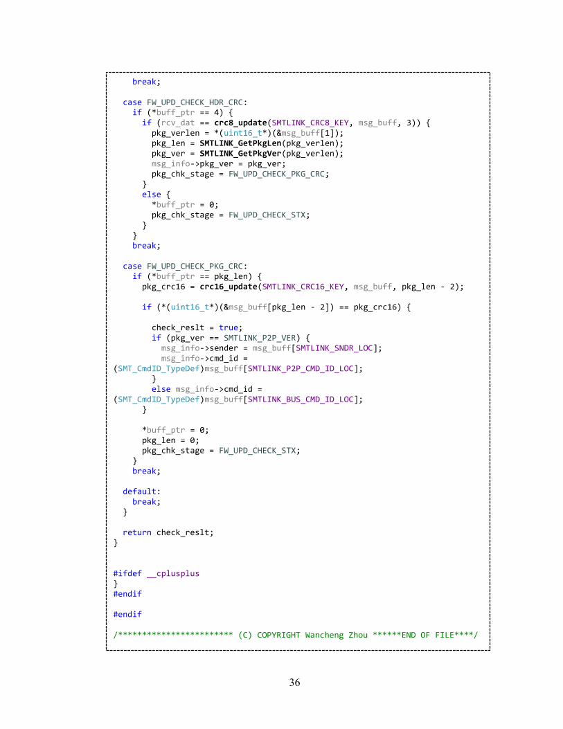
36
break; case FW_UPD_CHECK_HDR_CRC: if (*buff_ptr == 4) { if (rcv_dat == crc8_update(SMTLINK_CRC8_KEY, msg_buff, 3)) { pkg_verlen = *(uint16_t*)(&msg_buff[1]); pkg_len = SMTLINK_GetPkgLen(pkg_verlen); pkg_ver = SMTLINK_GetPkgVer(pkg_verlen); msg_info->pkg_ver = pkg_ver; pkg_chk_stage = FW_UPD_CHECK_PKG_CRC; } else { *buff_ptr = 0; pkg_chk_stage = FW_UPD_CHECK_STX; } } break; case FW_UPD_CHECK_PKG_CRC: if (*buff_ptr == pkg_len) { pkg_crc16 = crc16_update(SMTLINK_CRC16_KEY, msg_buff, pkg_len - 2); if (*(uint16_t*)(&msg_buff[pkg_len - 2]) == pkg_crc16) { check_reslt = true; if (pkg_ver == SMTLINK_P2P_VER) { msg_info->sender = msg_buff[SMTLINK_SNDR_LOC]; msg_info->cmd_id = (SMT_CmdID_TypeDef)msg_buff[SMTLINK_P2P_CMD_ID_LOC]; } else msg_info->cmd_id = (SMT_CmdID_TypeDef)msg_buff[SMTLINK_BUS_CMD_ID_LOC]; } *buff_ptr = 0; pkg_len = 0; pkg_chk_stage = FW_UPD_CHECK_STX; } break; default: break; } return check_reslt; } #ifdef __cplusplus } #endif #endif /************************ (C) COPYRIGHT Wancheng Zhou ******END OF FILE****/