compact-2d · compact f 2 f via planning incremental routing placement row splitting post- tier -...
TRANSCRIPT

Compact-2D:A Physical Design Methodology to Build
Commercial-Quality F2F-Bonded 3D ICs
Bon Woong Ku, Kyungwook Chang, and Sung Kyu Lim
Georgia Tech Computer-Aided Design LAB
Georgia Institute of Technology

2/26
• Introduction
– Advanced face-to-face (F2F) wafer-level bonding
– Issues the state-of-the-art flow for F2F-bonded 3D ICs has
• Compact-2D flow
– Area-optimal, low-power, timing-reliable, high-quality F2F-bonded 3D IC
physical design flow
– We use commercial 2D P&R engines
• Experiment results
– The impact of Compact-2D flow step-by-step
• Summary
Contents

3/263D IC Commercialization in Full Swing
Source: AMD, IMEC, Hynix
55μm
HBM2GDDR5
Off-chip Memory
Silicon Die Logic Die
Interposer
Package
Substrate
CPU / GPU
Stacked Memory
DRAM Core die
DRAM Core die
DRAM Core die
DRAM Core die
Base die μBump μBump
μBump
TSV
• HBM2 outperforms GDDR5 with only a 55μm pitch of 3D contact
Bandwidth: 800%↑
Power consumption: 52%↓
Scalable memory density solution: # of stacks
Splendid form factor savings

4/26
• Hybrid wafer-to-wafer (W2W) bonding technology
– Direct Cu-to-Cu / Oxide-to-Oxide bonding enables a 1μm pitch of 3D contact
– Close to commercialization for logic applications
Advanced Face-to-Face (F2F) Integration
(d): A.Jouve et al., 1μm Pitch direct hybrid bonding with <300nm wafer-to-wafer overlay accuracy, IEEE S3S, 2017.

Issues with State-of-the-Art

6/26
• Goal
– Conduct placement for two-tier F2F-bonded 3D IC
– Footprint is 50% as small as that of 2D IC counterpart
– How can 2D placer handle the overlaps between the cells?
• Shrunk-2D
– Shrink the cells and interconnects by 50%
– Commercial 2D placer can give high quality 3D placement
Shrunk-2D:How to Use 2D Placer for 3D Placement?
Shrunk 2D Cell ExpansionPlacement-driven FM min-cut
Tier partitioning
Original 2D Std. Cells
Shrunk 2D Std. Cells
(50% area)
S.Panth et. al. “Placement-driven partitioning for congestion mitigation in monolithic 3D IC designs”, ISPD 2014

7/26
• Goal
– For inter-tier 3D route, how can 2D router decide the F2F via locations?
• Shrunk-2D
– Routing with 3D tech / macro LEF and extracting the F2F vias as I/O ports
Shrunk-2D:How to Use 2D Router for 3D Routing?
Create separate
Verilog/DEF for each tier
3D tech LEF
M1:Die1
M6:Die1
M6:Die2
M1:Die2
F2F via
3D macro LEF
Bottom
Cell
Top
Cell
F2F via planning
Die1
Die2

8/26
• Shrinking cell & interconnect geometries
– Shrunk-2D requires P&R engines and design rule checkers that target one
node smaller technology, which is both challenging and costly
• Inaccurate RC parasitics of shrunk interconnect
– The original parasitic database causes inaccurate parasitics
Four Issues with Shrunk-2D
7nm Tech.
Cell / Interconnect
5nm Tech.-sized
Cell / Interconnect
Shrinking5nm P&R with 7nm engines?
Restoring
14nm
40n
m
20nm40
nm
Shrunk-2D
R = 0.125ρ
F2F
R = 0.0875ρ (x0.7)

9/26
• Ignore inter-tier 3D routing overhead
– Any inter-tier 3D routes require the full metal stacks for both tiers
– Nevertheless, there is no optimization step after Shrunk-2D design
• Discard earlier 3D routing
– Routing from scratch might cause redundant detour and timing violations
Four Issues with Shrunk-2D
Shrunk-2D F2F via planning
F2F via planning step
Length = 242.805um
Resistance = 1300ohm
Final Die0 step
Length = 300.347um
Resistance = 2176ohm

Our New Solution: Compact-2D

11/26
• When using a 2D commercial P&R engine for F2F-bonded 3D IC
– Avoid shrinking, Contract the entire placement
– Do not ignore 3D routing overhead, Supports post tier-partitioning opt.
– Do not discard the routing result at post-TP opt., Recycle it
Our Winning Formula
Compact-2D Design
Interconnect RC Scaling
Memory Preplacement
Memory Expansion
Memory Flattening
Tier Partitioning
Compact F2F Via Planning
Incremental Routing
Placement Row Splitting
Post-Tier-PartitioningOptimization
Conventional P&R steps 3D Timing & Power Analysis
Placement Contraction

12/26
• Compact-2D’s solution
– After conventional 2D design steps are done using the original layout objects,
contracting the placement solution linearly to fit into F2F design footprint
• New need for Interconnect RC scaling
– Delay with 0.707x scaled RC in Compact-2D = Delay with 1.0x RC in F2F design
Compact-2D:How to Avoid Geometry Shrinking?
W
H
(A,B) Contracting
0.707W
0.707H(0.707A,0.707B)
Compact-2D Placement Contraction F2F-bonded 3D IC
X
Y
HPWL = X+Y
Delay = L HPWL = 0.707(X+Y)
Delay = L
HPWL = 0.707(X+Y)
Delay = L
Top Bottom
Interconnect
With Scaled RC

13/26
Compact-2D:How to Handle Memory Macros?
• Compact-2D’s solution
– Memory macro boundaries should be expanded to 1.414x
Contracting with the original macro pin location Contracting with the expanded macro pin location
Memory Expansion &
Preplacement
Memory Flattening Compact-2D designPlacement
Contraction
14/26
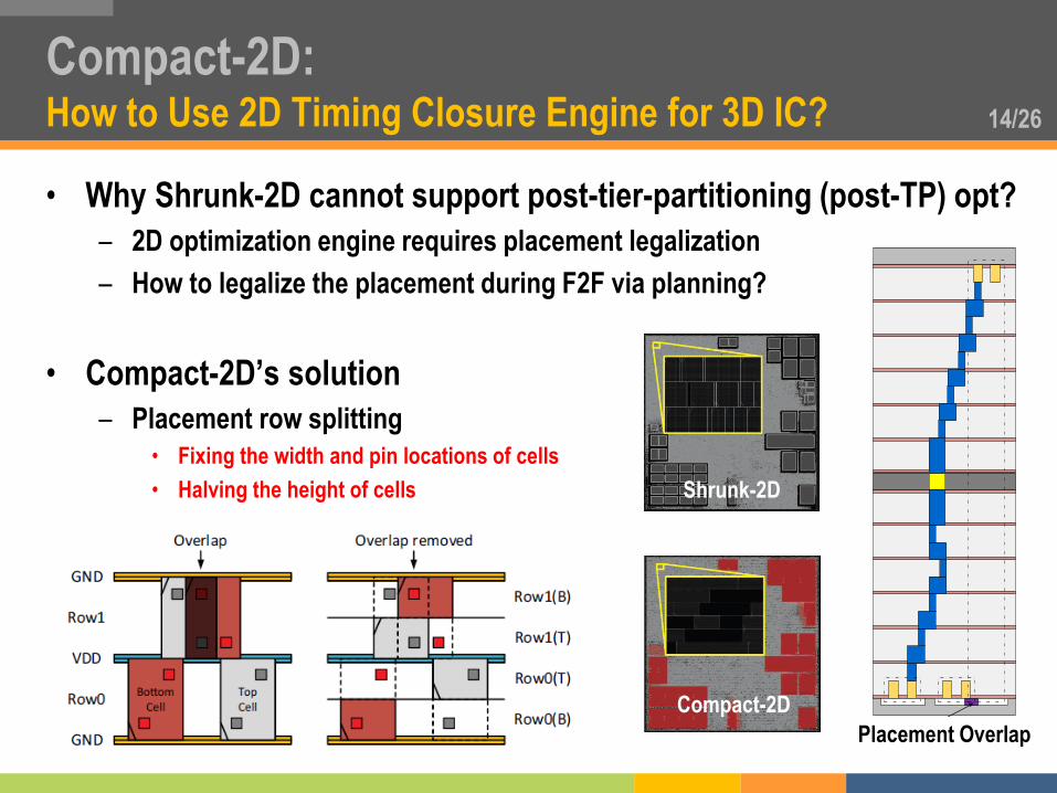
• Why Shrunk-2D cannot support post-tier-partitioning (post-TP) opt?
– 2D optimization engine requires placement legalization
– How to legalize the placement during F2F via planning?
• Compact-2D’s solution
– Placement row splitting
• Fixing the width and pin locations of cells
• Halving the height of cells
Compact-2D:How to Use 2D Timing Closure Engine for 3D IC?
Placement overlap
Shrunk-2D
Placement Overlap
Compact-2D

15/26
• Compact-2D’s solution
– Construct a graph with wiring segments (polygons, vias, cell pins, ports)
• Edge contains the routing information
– Disconnecting a 3D net into multiple subnets on separate tiers
Compact-2D:How to Preserve 3D Net Routing during F2F Via Insertion?
F2F via planning Compact F2F
via planning
Incremental
Routing
Shrunk-2D flow Compact-2D flow
Die1 Die1
Die2
Iterative
Routing
Verilog / DEF
for each die
w/ subnet routes
Die2
Verilog / DEF
for each die
w/o subnet routes

Experimental Results

17/26GDS Die Shots (Commercial 28nm PDK)
OpenSparc T2 single core (SPC) 2D and C2D
LDPC 2D and C2D AES 2D and C2D JPEG 2D and C2D
F2F vias in C2D-SPC
Our designs and simulations are commercial quality!

18/26Shrunk-2D vs. Compact-2D
2D Shrunk-2D Savings% Compact-2D Savings%
Target timing 1GHz
Total WL (m) 15.36 11.77 23.4% 11.55 24.8%
F2F Via # - 154,127 - 193,487 -
Footprint (mm2) 2.53 1.26 50.2% 1.26 50.2%
Total Power (mW) 338.20 300.87 11.0% 299.88 11.3%
Cell Power (mW) 82.12 79.11 3.7% 79.07 3.7%
Net Power (mW) 183.26 153.33 16.3% 150.86 17.7%
Worst. Neg. Slack (ps) -27.65 -52.52 -89.9% -25.99 6.0%
Total Neg. Slack (ps) -832.85 -846.94 -1.7% -136.75 83.6%
• OpenSparc T2 single core (1.0GHz)
– F2F via size = 500nm, pitch = 1μm, R = 0.5Ω, C = 0.2fF
– Switching activity: 0.1 for PIs, Reg. out pins / 2.0 for Clock

19/26Rigorous Area Saving with Compact-2D
Footprint (3D/2D) 50% 45% 40% 35% 30%
RC Scaling 0.707 0.671 0.632 0.592 0.548
LDPC
Std. Cell Area (mm2) 0.180 0.178 0.177 0.172 0.169
3D Place. Util. per Die 58.31% 63.92% 72.03% 79.69% 91.29%
Place. Util (3D/2D) 87.83% 96.30% 108.50% 120.04% 137.51%
Total Power (mW) 179.23 174.48 167.70 158.03 153.85
Footprint (3D/2D) 50% 47% 44% 41% 38%
RC Scaling 0.707 0.686 0.663 0.640 0.616
AES-128
Std. Cell Area (mm2) 0.359 0.356 0.355 0.355 0.355
3D Place. Util. per Die 70.10% 73.88% 78.99% 84.58% 91.43%
Place. Util (3D/2D) 95.09% 100.22% 107.15% 116.15% 124.03%
Total Power (mW) 331.68 330.49 324.54 323.39 322.18
20/26
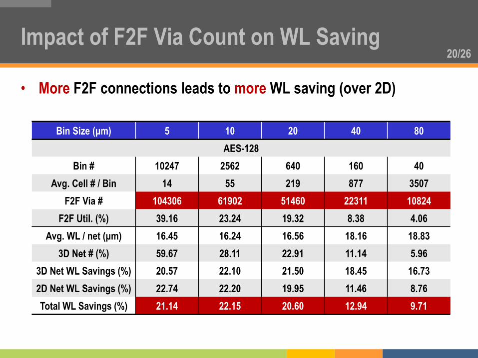
• More F2F connections leads to more WL saving (over 2D)
Impact of F2F Via Count on WL Saving
Bin Size (μm) 5 10 20 40 80
AES-128
Bin # 10247 2562 640 160 40
Avg. Cell # / Bin 14 55 219 877 3507
F2F Via # 104306 61902 51460 22311 10824
F2F Util. (%) 39.16 23.24 19.32 8.38 4.06
Avg. WL / net (μm) 16.45 16.24 16.56 18.16 18.83
3D Net # (%) 59.67 28.11 22.91 11.14 5.96
3D Net WL Savings (%) 20.57 22.10 21.50 18.45 16.73
2D Net WL Savings (%) 22.74 22.20 19.95 11.46 8.76
Total WL Savings (%) 21.14 22.15 20.60 12.94 9.71

21/26
• Further optimizes buffer insertion and gate sizing
– Improves timing significantly
Impact of Post-Tier Partitioning Optimization
LDPC benchmarkBefore
3D Routing
After
3D Routing
No-Opt Yes-Opt Savings
Total Cell # 65187 65187 65271 -0.1%
Worst Neg. Slack (ps) -7.42 -43.57 -24.23 44.4%
Total Neg. Slack (ps) -341.86 -2637.13 -222.99 91.5%
Total Pos. Slack (ps) 19194.40 17042.80 27072.40 58.8%
Violated Path # 20 383 27 93.0%
Total Power 179.23 178.25 178.49 -0.1%

22/26Impact of Incremental Routing
LDPC BenchmarkBefore
Tier-by-tier Routing
After
Tier-by-tier Routing
Iterative
Routing
Incremental
RoutingSavings
Total WL (m) 2.721 2.754 2.750 0.1%
Worst Neg. Slack (ps) -24.23 -45.17 -25.16 44.3%
Total Neg. Slack (ps) -222.99 -5771.74 -1599.73 72.3%
Total Pos. Slack (ps) 27072.40 11257.00 15107.10 34.2%
Violated Path # 27 734 402 45.2%
Total Power 178.49 179.53 179.15 0.2%
• Avoids significant routing changes
– Improves timing significantly

23/26
• Compact-2D gives
– Superior saving in silicon area, wirelength, and power
– More savings for wire-dominated designs
Compact-2D vs. 2D at Iso-performance
LDPC, 2GHZ AES=128, 5.4GHz JPEG, 2.16GHz
Design 2D C2D Savings 2D C2D Savings 2D C2D Savings
Silicon Area (mm2) 0.308 0.261 15.6% 0.512 0.482 6.0% 1.334 1.254 6.0%
F2F Via # - 21K - - 63K - - 121K -
Std. Cell Area (mm2) 0.205 0.179 12.7% 0.378 0.361 4.4% 0.982 0.944 3.9%
Total WL (m) 3.8 2.5 33.6% 2.9 2.2 22.9% 5.8 4.6 20.2%
Switching Power 193.9 136.9 29.4% 250.8 223.7 10.8% 415.8 385.9 7.2%
Cell Internal Power 33.0 28.8 12.7% 113.6 108.4 4.6% 195.1 189.9 2.7%
Leakage Power 11.1 8.2 26.1% 17.5 16.1 8.0% 30.2 28.5 5.6%
Total Power 237.8 174.0 26.8% 381.9 348.2 8.8% 641.1 604.4 5.7%

24/26
• When using a 2D commercial P&R engine for F2F-bonded 3D IC
– Avoid shrinking, Contract the entire placement
– Do not ignore 3D routing overhead, Supports post tier-partitioning opt.
– Do not discard the routing result at post-TP opt., Recycle it
Recap: Our Winning Formula
Compact-2D Design
Interconnect RC Scaling
Memory Preplacement
Memory Expansion
Memory Flattening
Tier Partitioning
Compact F2F Via Planning
Incremental Routing
Placement Row Splitting
Post-Tier-PartitioningOptimization
Conventional P&R steps 3D Timing & Power Analysis
Placement Contraction

25/26
• Compact-2D flow
– Full-chip RTL-to-GDSII physical design solution
– Offers a commercial-quality F2F-bonded 3D ICs using a commercial 2D engine
• This flow is capable of
– Utilizing the technology files and design rules of the target technology node
– Optimizing the area savings more flexibly by placement contraction
– Supporting post-TP opt. to address inter-tier 3D routing overhead
– Minimizing the perturbation in tier-by-tier routing from post-TP opt.
• Compact-2D achieves
– 26.8% of power reduction, and 15.6% silicon area savings over 2D ICs
Summary


Supplement

28/26Commercial EDA Flow for F2F Not Available
3D-Contact Level Global Semi-global Intermediate Local FEOL
Two-tier Stack
Schematic
3D Technology
Die-to-Die
Die-to-Wafer
Die-to-Interposer
Parallel Wafer Processing
Wafer-to-Wafer Bonding
Monolithic FEOL Processing
Active Layer Deposition
Integration
SchemeBack-to-Back / Face-to-Face Face-to-Back
Contact Pitch 40μm → 5μm 5μm → 1μm 2μm → 500nm 200nm → 100nm < 100nm
Relative Density 1 → 64 64 → 1600 400 → 6400 40000 → 160000 > 160000
Partitioning Dies Blocks Gates (Std. Cells) Transistors
2nd FEOL
After StackingMulti-tier
FEOL
3D partitioning / placement: new EDA problems
A new design solution is required
E. Beyne. The 3-d interconnect technology landscape. IEEE Design Test, 2016.
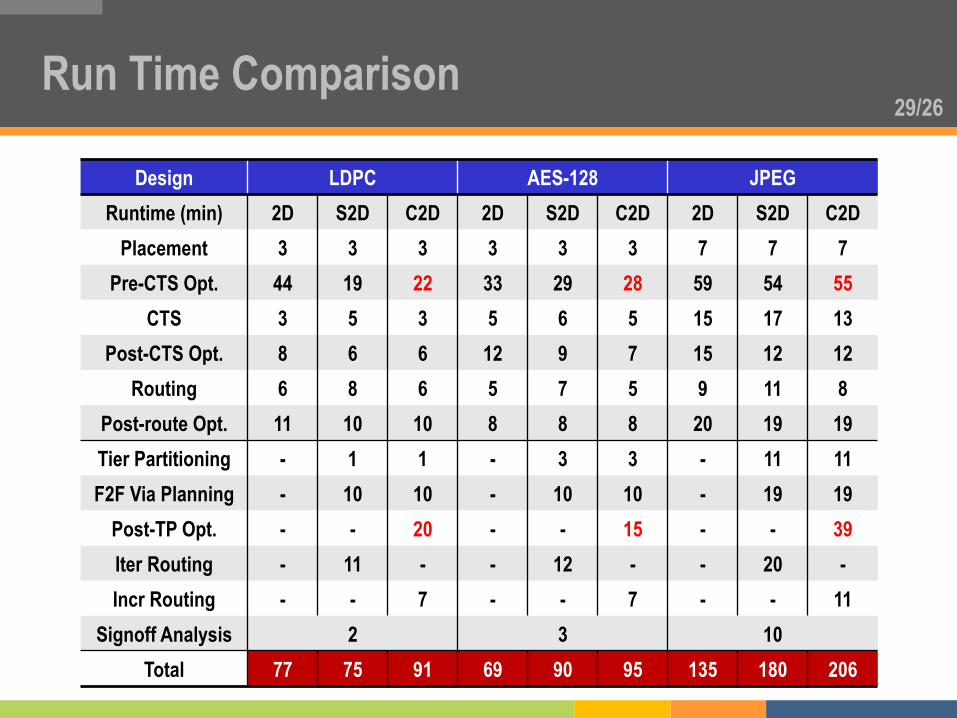
29/26Run Time Comparison
Design LDPC AES-128 JPEG
Runtime (min) 2D S2D C2D 2D S2D C2D 2D S2D C2D
Placement 3 3 3 3 3 3 7 7 7
Pre-CTS Opt. 44 19 22 33 29 28 59 54 55
CTS 3 5 3 5 6 5 15 17 13
Post-CTS Opt. 8 6 6 12 9 7 15 12 12
Routing 6 8 6 5 7 5 9 11 8
Post-route Opt. 11 10 10 8 8 8 20 19 19
Tier Partitioning - 1 1 - 3 3 - 11 11
F2F Via Planning - 10 10 - 10 10 - 19 19
Post-TP Opt. - - 20 - - 15 - - 39
Iter Routing - 11 - - 12 - - 20 -
Incr Routing - - 7 - - 7 - - 11
Signoff Analysis 2 3 10
Total 77 75 91 69 90 95 135 180 206

30/26Compact-2D vs. 2D at Iso-performance
LDPC, 2GHZ AES=128, 5.4GHz JPEG, 2.16GHz
Design 2D C2D Savings 2D C2D Savings 2D C2D Savings
Footprint (mm2) 0.308 0.130 57.8% 0.512 0.241 53.0% 1.334 0.627 53.0%
Silicon Area (mm2) 0.308 0.261 15.6% 0.512 0.482 6.0% 1.334 1.254 6.0%
F2F Via # - 21575 - - 63211 - - 121357 -
Cell # 77024 64610 16.1% 147483 140960 4.4% 312451 284884 8.8%
Std. Cell Area (mm2) 0.205 0.179 12.7% 0.378 0.361 4.4% 0.982 0.943 3.9%
Total WL (m) 3.8 2.5 33.6% 2.9 2.2 22.9% 5.8 4.6 20.2%
Switching Power 193.9 136.9 29.4% 250.8 223.7 10.8% 415.8 385.9 7.2%
Cell Internal Power 33.0 28.8 12.7% 113.6 108.4 4.6% 195.1 189.9 2.7%
Leakage Power 11.1 8.2 26.1% 17.5 16.1 8.0% 30.2 28.5 5.6%
Total Power 237.8 174.0 26.8% 381.9 348.2 8.8% 641.1 604.4 5.7%

31/26
• For Compact-2D to perform 3D placement
– There are two separate steps to decide 3D placement solution
• First, horizontal locations (X,Y) by Compact-2D design
• Second, vertical locations (Z) by tier-partitioning
• For the 2D placer to become an ideal 3D placer, it needs to support
– Placement row splitting
• To accommodate all synthesized gates on the final F2F design footprint
– Local area-skew constraint over split rows
• For the balanced placement utilization in different dies
– Design rule checkers for the pins outside the macro boundary
• This is the main reason why incremental routing needs final DRV fixing
Lessons for 2D Engines to Perform 3D P&R

32/26
• For Compact-2D to perform 3D optimization
– A parasitic corner for the full 3D metal stack is required
– Timing corners for both dies are required
• For the 2D router to become an ideal 3D router it needs to support
– Routing M6:bottom and M6:top in the same routing direction
• Currently, this feature is not fully supported in the commercial 2D router
– More sophisticated design rules / parasitic modeling for 3D contacts
• Currently, only pitch constraint / ∏-modeling of 3D contacts are used
– Design rule checkers for the pins outside the macro boundary
• This is the main reason why incremental routing needs final DRV fixing
Lessons for 2D Engines to Perform 3D P&R

33/26
• Handling more than two tiers
– Foreseeable problems:
• 𝟏/ 𝒏 scaling factors in interconnect RC scaling / placement contraction
• n-way balanced tier partitioning schemes
• n-placement row splitting in the Compact F2F via planning
• F2F / B2B gate-level inter-tier connections with different pitches
• Building commercial-quality monolithic 3D ICs
– Foreseeable problems:
• Accurate parasitic / timing corners for post-TP optimization
• Sophisticated tier-partitioning algorithm
– Given device / interconnect inter-tier variations in monolithic 3D ICs
Future Directions of Compact-2D