common base (cb) amplifier - indian institute of...
TRANSCRIPT
9/28/2017
1
Analog Electronics(Course Code: EE314)
Lecture 14‐15: CB and CE Amplifiers
Indian Institute of Technology Jodhpur, Year 2017
Course Instructor: Shree PrakashTiwari
Email: [email protected]
b h //h / /Webpage: http://home.iitj.ac.in/~sptiwari/
Course related documents will be uploaded on http://home.iitj.ac.in/~sptiwari/EE314/
1
Note: The information provided in the slides are taken form text books for microelectronics (including Sedra & Smith, B. Razavi), and various other resources from internet, for teaching/academic use only
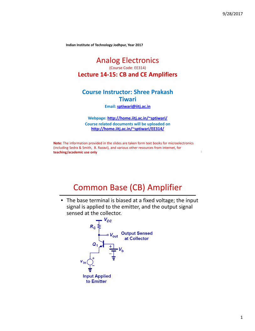
Common Base (CB) Amplifier
• The base terminal is biased at a fixed voltage; the input signal is applied to the emitter, and the output signal sensed at the collector.sensed at the collector.

9/28/2017
2
Small‐Signal Analysis of CB Core
• The voltage gain of a CB stage is gmRC, which is identical to that of a CE stage in magnitude and opposite in phaseopposite in phase.
Cmv RgA
Tradeoff between Gain and Headroom
• To ensure that the BJT operates in active mode, the voltage drop across RC cannot exceed VCC‐VBE.
T
BECCC
T
Cv V
VVR
V
IA

9/28/2017
3
Simple CB Stage Example
VCC = 1.8VIC = 0.2mAIS = 5x10-17 AS
= 100
Simple CB Stage Example
VCC = 1.8VIC = 0.2mAIS = 5x10-17 AS
= 100
R
2.172230130
1 Cmv RgA
k7.67 ,k3.22
2010 Choose
if 354.1
21
211
121
2
RR
RR
VAII
IIVRR
RVV
CCB
BCCb

9/28/2017
4
Input Impedance of a CB Stage
• The input impedance of a CB stage is much smaller than that of a CE stage.
1 A
min V
gR if
1
CB Stage with Source Resistance
• With the inclusion of a source resistance, the input signal is attenuated before it reaches the emitter of the amplifier; therefore, the voltage gain is lowered.the amplifier; therefore, the voltage gain is lowered. – This effect is similar to CE stage emitter degeneration.
S
m
Cv
Rg
RA
1

9/28/2017
5
Practical Example of a CB Stage
• An antenna usually has low output impedance; therefore, a correspondingly low input impedance is required for the following stagerequired for the following stage.
Output Impedance of a CB Stage
• The output impedance of a CB stage is equal to RC in parallel with the impedance looking into the collector.
12
1
||
||)||(1
outCout
EOEmout
RRR
rRrrRgR
9/28/2017
6
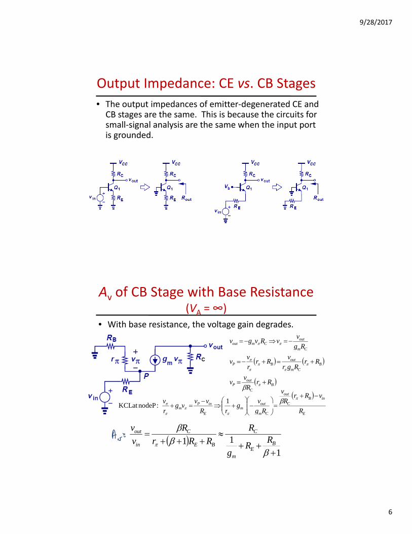
Output Impedance: CE vs. CB Stages
• The output impedances of emitter‐degenerated CE and CB stages are the same. This is because the circuits for small‐signal analysis are the same when the input portsmall signal analysis are the same when the input port is grounded.
Av of CB Stage with Base Resistance (VA = ∞)
• With base resistance, the voltage gain degrades.
outCmout Rg
vvRvgv
BC
outP
BCm
outBP
Cm
RrR
vv
RrRgr
vRr
r
vv
Rg
inB
C
out
outinP
vRrR
vv
gvv
vgv
1:PnodeatKCL
ECmm
Em RRg
grR
vgr
:P nodeat KCL
1
11
BE
m
C
BE
C
in
out
RR
g
R
RRr
R
v
v
9/28/2017
7
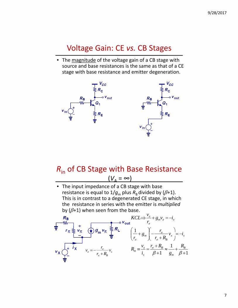
Voltage Gain: CE vs. CB Stages
• The magnitude of the voltage gain of a CB stage with source and base resistances is the same as that of a CE stage with base resistance and emitter degeneration.stage with base resistance and emitter degeneration.
Rin of CB Stage with Base Resistance(VA = ∞)
• The input impedance of a CB stage with base resistance is equal to 1/gm plus RB divided by (+1). This is in contrast to a degenerated CE stage, in whichThis is in contrast to a degenerated CE stage, in which the resistance in series with the emitter is multipliedby (+1) when seen from the base.
1
xm
ivr
g
ivgr
vKCL
1
1
1
B
m
B
x
xin
xxB
m
R
g
Rr
i
vR
ivRr
gr
xB
vRr
rv
9/28/2017
8
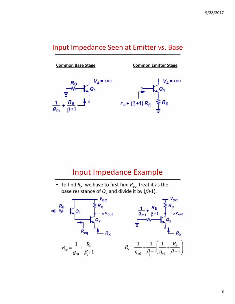
Input Impedance Seen at Emitter vs. Base
Common Base Stage Common Emitter Stage
Input Impedance Example
• To find RX, we have to first find Req, treat it as the base resistance of Q2 and divide it by (+1).
1
1
1
11
12 B
mmx
R
ggR
1
1
1
B
meq
R
gR

9/28/2017
9
Biasing of CB Stage
• RE is necessary to provide a path for the bias current IE to flow, but it lowers the input impedance.
1
inSEmE
Ein
Sin
inX v
RRgR
Rv
RR
Rv
1
Em
E
Em
Em
Em
in Rg
R
Rg
Rg
Rg
R
11
1
||1
SEmE
ECm
in
out
in
X
X
out
in
outv
RRgR
RRg
v
v
v
v
v
v
v
vA
1
Reduction of Input Impedance Due to RE• The reduction of input impedance due to RE is undesirable because it shunts part of the input current to ground instead of to Q1 (and RC).current to ground instead of to Q1 (and RC).
Choose RE >> 1/gm , i.e. ICRE >> VT
9/28/2017
10
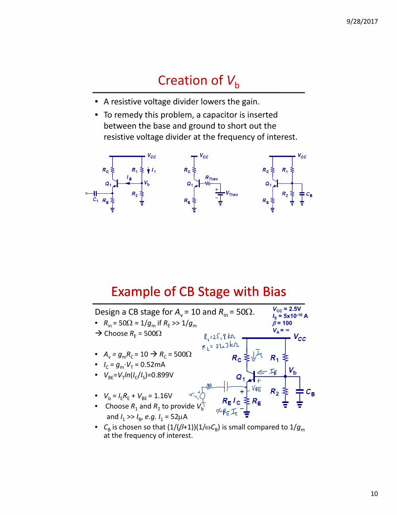
Creation of Vb
• A resistive voltage divider lowers the gain.
• To remedy this problem, a capacitor is inserted between the base and ground to short out the resistive voltage divider at the frequency of interest.
Example of CB Stage with Bias
Design a CB stage for Av = 10 and Rin = 50.• Rin = 50≈ 1/gm if RE >> 1/gm Choose R = 500
VCC = 2.5VIS = 5x10-16 A= 100VA = ∞
Example of CB Stage with Bias
Choose RE = 500
• Av = gmRC = 10 RC = 500• IC = gm∙VT = 0.52mA
• VBE=VTln(IC/IS)=0.899V
A
• Vb = IERE + VBE = 1.16V
• Choose R1 and R2 to provide Vb
and I1 >> IB, e.g. I1 = 52A• CB is chosen so that (1/(+1))(1/CB) is small compared to 1/gm
at the frequency of interest.

9/28/2017
11
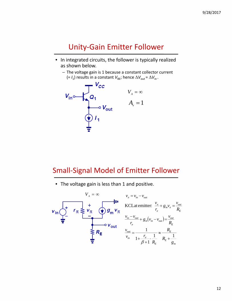
Emitter Follower (Common Collector Amplifier)
Emitter Follower Core
• When the input voltage (Vin) is increased by Vin, the collector current (and hence the emitter current) increases, so that the output voltage (V t) is increased.increases, so that the output voltage (Vout) is increased.
• Note that Vin and Vout differ by VBE.
9/28/2017
12
Unity‐Gain Emitter Follower
• In integrated circuits, the follower is typically realized as shown below.
Th lt i i 1 b t t ll t t– The voltage gain is 1 because a constant collector current (= I1) results in a constant VBE; hence Vout = Vin .
1vA
AV
v
Small‐Signal Model of Emitter Follower
• The voltage gain is less than 1 and positive.
V
E
outoutinm
outin
E
outm
outin
Rv
R
vvvg
r
vv
R
vvg
r
v
vvv
1
:emitterat KCL
AV
mE
E
E
in
out
gR
R
R
rv
v11
11
1
9/28/2017
13
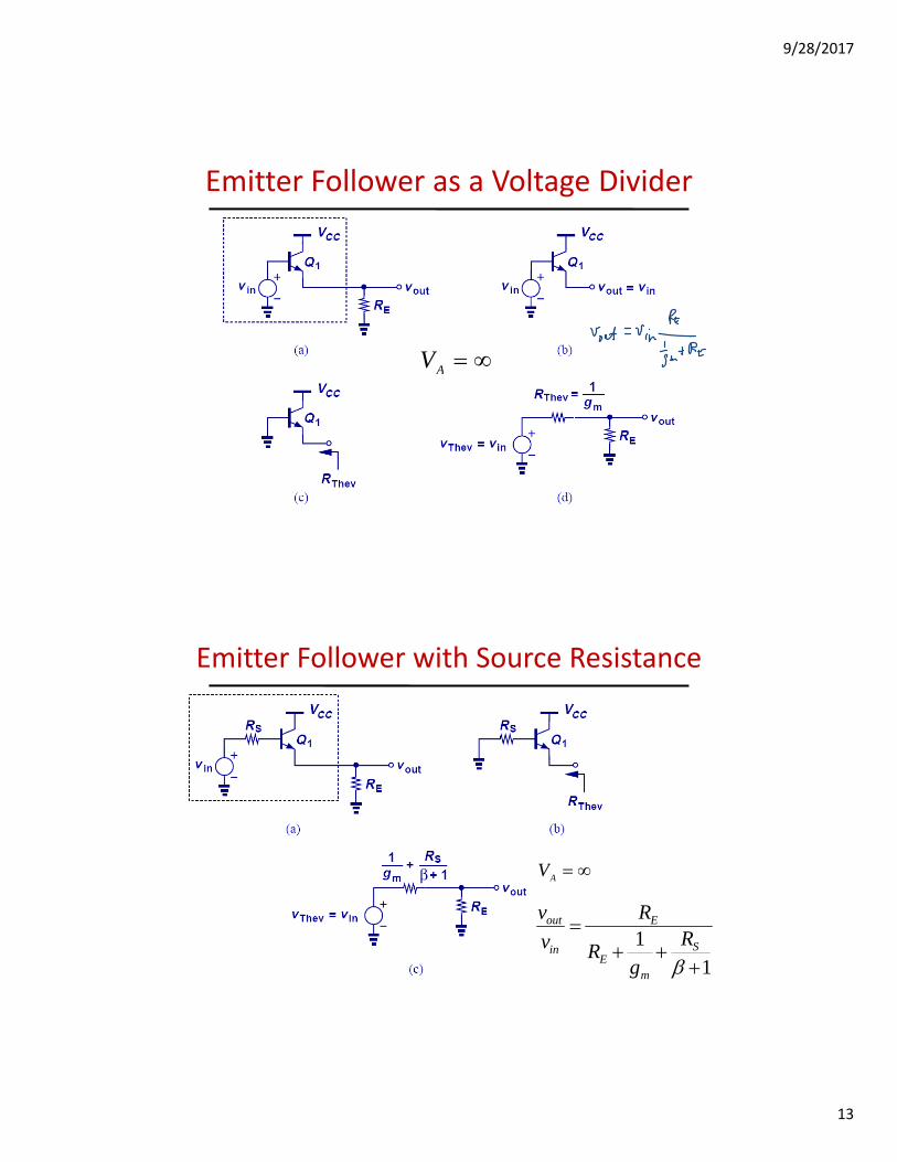
Emitter Follower as a Voltage Divider
AV
Emitter Follower with Source Resistance
AV
11
S
mE
E
in
out
Rg
R
R
v
v

9/28/2017
14
Input Impedance of Emitter Follower
• The input impedance of an emitter follower is the same as that of a CE stage with emitter degeneration (whose input impedance does not depend on the(whose input impedance does not depend on the resistance between the collector and VCC).
AV
Ex
xin Rr
i
vR )1(
Effect of BJT Current Gain
• There is a current gain of (+1) from base to emitter.
• Effectively, the load resistance seen from the base is multiplied by (+1).
9/28/2017
15
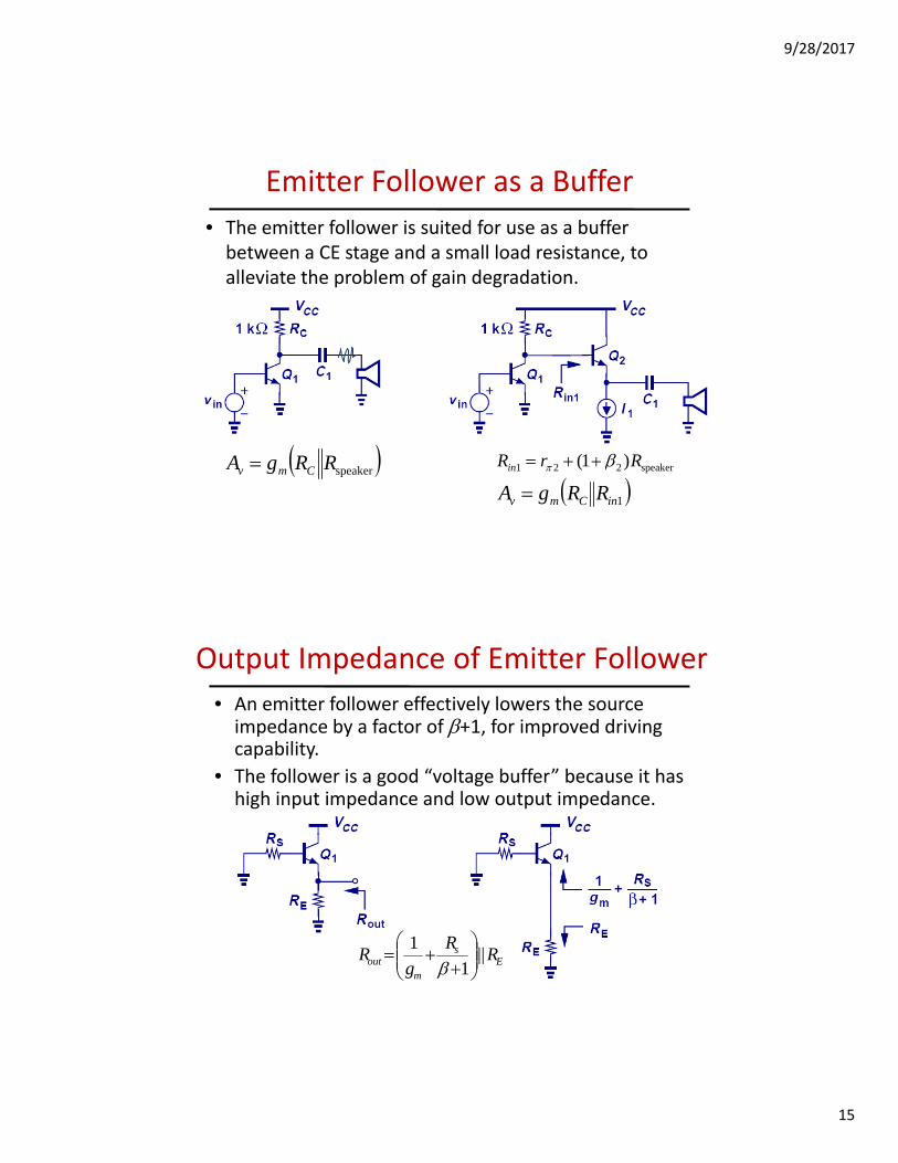
Emitter Follower as a Buffer
• The emitter follower is suited for use as a buffer between a CE stage and a small load resistance, to alleviate the problem of gain degradationalleviate the problem of gain degradation.
speaker221 )1( RrRin
1inCmv RRgA speakerRRgA Cmv
Output Impedance of Emitter Follower
• An emitter follower effectively lowers the source impedance by a factor of +1, for improved driving capability.capability.
• The follower is a good “voltage buffer” because it has high input impedance and low output impedance.
Es
mout R
R
gR ||
1
1
9/28/2017
16
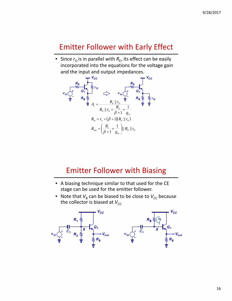
Emitter Follower with Early Effect
• Since rO is in parallel with RE, its effect can be easily incorporated into the equations for the voltage gain and the input and output impedancesand the input and output impedances.
OEv R
rRA
1||
OE
m
sout
OEin
m
SOE
v
rRg
RR
rRrR
gR
rR
||||1
1
||1
11
||
Emitter Follower with Biasing
• A biasing technique similar to that used for the CE stage can be used for the emitter follower.
N t th t V b bi d t b l t V b• Note that VB can be biased to be close to VCC because the collector is biased at VCC.
9/28/2017
17
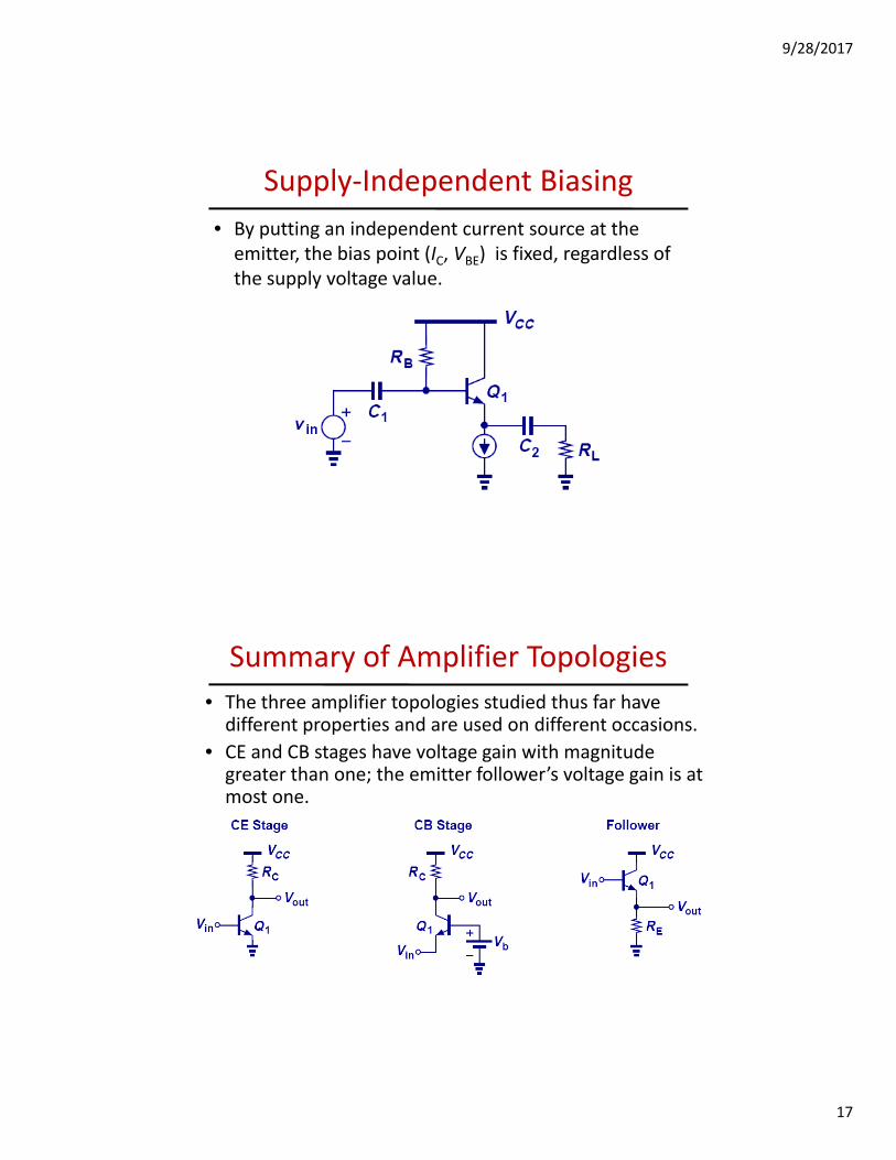
Supply‐Independent Biasing
• By putting an independent current source at the emitter, the bias point (IC, VBE) is fixed, regardless of the supply voltage valuethe supply voltage value.
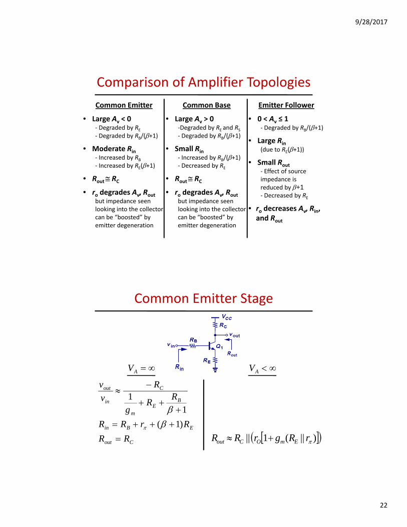
Summary of Amplifier Topologies
• The three amplifier topologies studied thus far have different properties and are used on different occasions.
• CE and CB stages have voltage gain with magnitude• CE and CB stages have voltage gain with magnitude greater than one; the emitter follower’s voltage gain is at most one.
9/28/2017
18
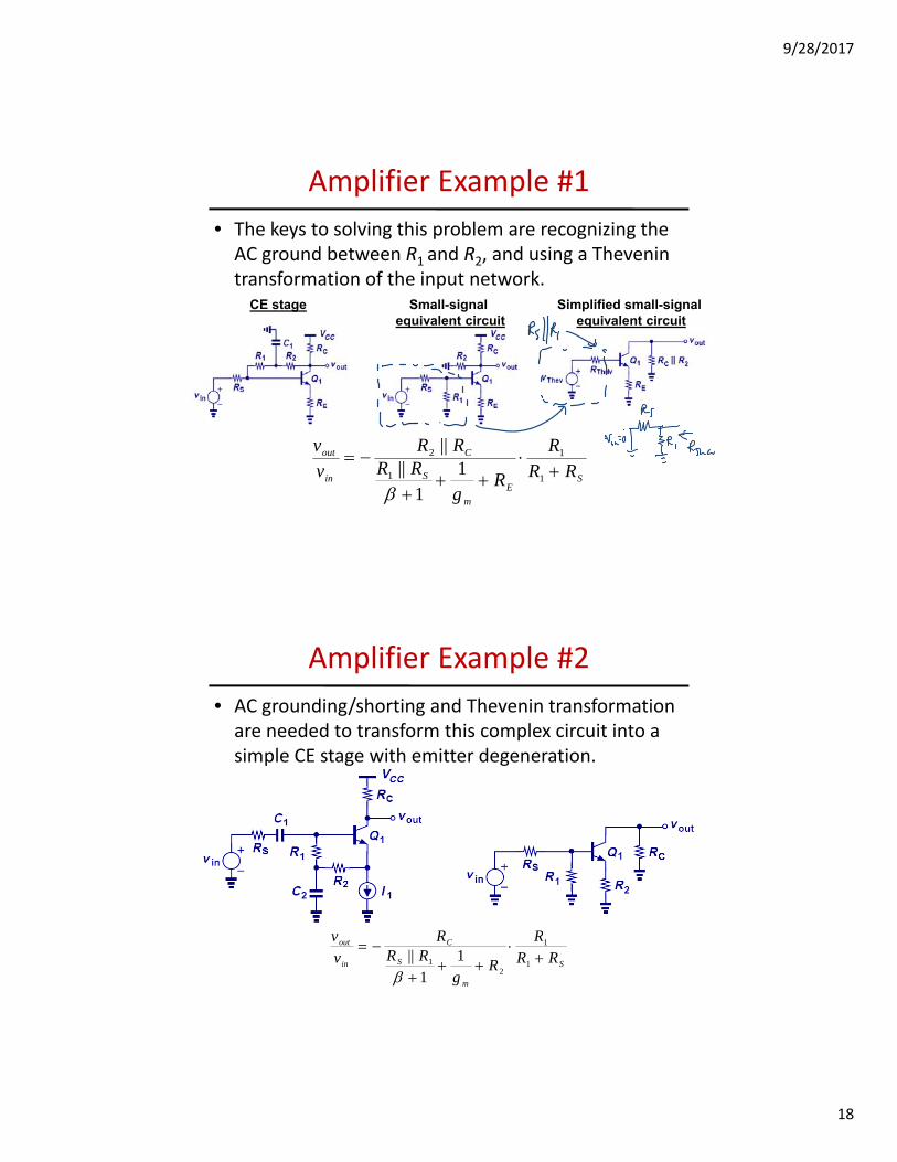
Amplifier Example #1
• The keys to solving this problem are recognizing the AC ground between R1 and R2, and using a Thevenin transformation of the input networktransformation of the input network.
CE stage Small-signal equivalent circuit
Simplified small-signal equivalent circuit
SE
m
S
C
in
out
RRR
Rg
RRRR
vv
1
1
1
2
11
||||
Amplifier Example #2
• AC grounding/shorting and Thevenin transformation are needed to transform this complex circuit into a simple CE stage with emitter degenerationsimple CE stage with emitter degeneration.
S
m
S
C
in
out
RRR
Rg
RRR
vv
1
1
21 1
1||
9/28/2017
19
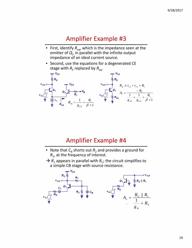
Amplifier Example #3• First, identify Req, which is the impedance seen at the emitter of Q2 in parallel with the infinite output impedance of an ideal current source.impedance of an ideal current source.
• Second, use the equations for a degenerated CE stage with RE replaced by Req.
121 RrrRin
1
1 1
2 R
gR
meq
111 1
21
121
Rgg
RA
mm
Cv
in
Amplifier Example #4
• Note that CB shorts out R2 and provides a ground for R1, at the frequency of interest.
R appears in parallel with R ; the circuit simplifies to R1 appears in parallel with RC; the circuit simplifies to a simple CB stage with source resistance.
Sm
Cv
Rg
RRA
1|| 1
9/28/2017
20
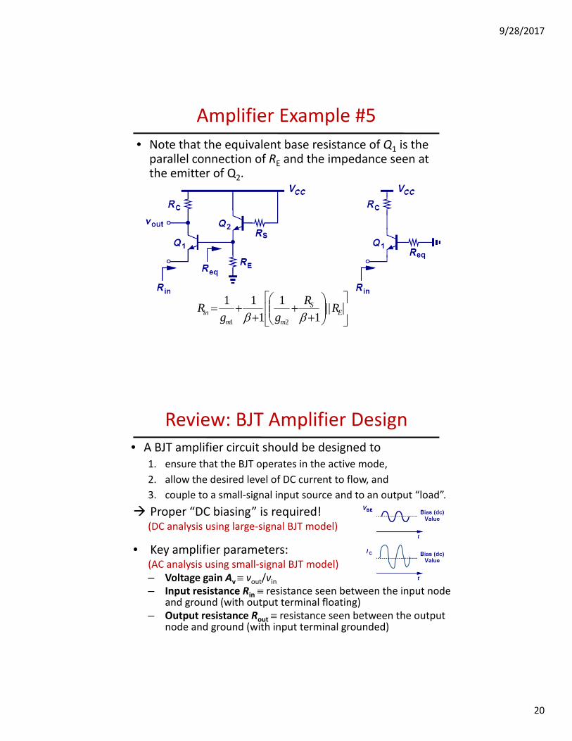
• Note that the equivalent base resistance of Q1 is the parallel connection of RE and the impedance seen at the emitter of Q2.
Amplifier Example #5
the emitter of Q2.
ES
mmin R
R
ggR ||
1
1
1
11
21
Review: BJT Amplifier Design• A BJT amplifier circuit should be designed to
1. ensure that the BJT operates in the active mode,
2 allow the desired level of DC current to flow and2. allow the desired level of DC current to flow, and
3. couple to a small‐signal input source and to an output “load”.
Proper “DC biasing” is required!(DC analysis using large‐signal BJT model)
• Key amplifier parameters: (AC analysis using small‐signal BJT model)(AC analysis using small‐signal BJT model)– Voltage gain Av vout/vin– Input resistance Rin resistance seen between the input node
and ground (with output terminal floating)– Output resistance Rout resistance seen between the output
node and ground (with input terminal grounded)

9/28/2017
21
Large‐Signal vs. Small‐Signal Models
• The large‐signal model is used to determine the DC operating point (VBE, VCE, IB, IC) of the BJT.
• The small‐signal model is used to determine how the output responds to an input signaloutput responds to an input signal.
• The voltage across an independent voltage source does not vary with time. (Its small‐signal voltage is always zero.)
It is regarded as a short circuit for small signal analysis
Small‐Signal Models for Independent Sources
It is regarded as a short circuit for small‐signal analysis.
Large-SignalModel
Small-SignalModel
• The current through an independent current source does not vary with time. (Its small‐signal current is always zero.)
It is regarded as an open circuit for small‐signal analysis.
9/28/2017
22
Comparison of Amplifier Topologies
Common Emitter
• Large Av < 0
Common Base
• Large Av > 0
Emitter Follower
• 0 < Av ≤ 1/‐ Degraded by RE
‐ Degraded by RB/(+1)
• Moderate Rin‐ Increased by RB‐ Increased by RE(+1)
• Rout RC
‐Degraded by RE and RS‐ Degraded by RB/(+1)
• Small Rin‐ Increased by RB/(+1)‐ Decreased by RE
• Rout RC
‐ Degraded by RB/(+1)
• Large Rin(due to RE(+1))
• Small Rout ‐ Effect of source impedance is d d b 1
• ro degrades Av, Routbut impedance seenlooking into the collector can be “boosted” by emitter degeneration
• ro degrades Av, Routbut impedance seenlooking into the collector can be “boosted” by emitter degeneration
reduced by +1‐ Decreased by RE
• ro decreases Av, Rin, and Rout
Common Emitter Stage
B
C
in
out
RR
R
v
v
1
AV AV
Cout
EBin
BE
m
in
RR
RrRR
Rg
)1(
1
)||(1|| rRgrRR EmOCout

9/28/2017
23
Common Base Stage
V
ES
E
BES
m
C
in
out
RR
RR
RRg
R
v
v
11
AV
EB
min R
R
gR
1
1
Cout RR )||(1|| rRgrRR EmOCout
AV
Emitter Follower
AV AV
11
S
mE
E
in
out
R
gR
R
v
v
S
mOE
OE
in
out
Rg
rR
rR
v
v
11
||
||
mg
Ein RrR )1(
Es
mout R
R
gR ||
1
1
OEm
sout
OEin
m
rRg
RR
rRrR
g
||||1
1
||1

9/28/2017
24
What next
• Cascode and Current Mirrors with BJT
• MOSFET fundamentals and Amplifiers
or
• MOSFET fundamentals and Amplifiers
• Cascode and Current Mirrors with BJT and MOSFET