commodore-64 service manual
DESCRIPTION
No DescriptionTRANSCRIPT

C64SM12*********
Welcome to Project 64!
The goal of Project 64 is to preserve Commodore 64 related documentsin electronic text format that might otherwise cease to exist with therapid advancement of computer technology and declining interest in 8-bit computers on the part of the general population. If you would liketo help by converting C64 related hardcopy documents to electronictexts please contact the manager of Project 64, Cris Berneburg, [email protected].
Extensive efforts were made to preserve the contents of the originaldocument. However, certain portions, such as diagrams, programlistings, and indexes may have been either altered or sacrificed dueto the limitations of plain vanilla text. Diagrams may have beeneliminated where ASCII-art was not feasible. Program listings may bemissing display codes where substitutions were not possible. Tablesof contents and indexes may have been changed from page numberreferences to section number references. Please accept our apologiesfor these limitations, alterations, and possible omissions.
Document names are limited to the 8.3 file convention of DOS. Thefirst characters of the file name are an abbreviation of the originaldocument name. The version number of the etext follows next. Afterthat a letter may appear to indicate the particular source of thedocument. Finally, the document is given a .TXT extension.
The author(s) of the original document and members of Project 64 makeno representations about the accuracy or suitability of this materialfor any purpose. This etext is provided "as-is". Please refer to thewarantee of the original document, if any, that may included in thisetext. No other warantees, express or implied, are made to you as tothe etext or any medium it may be on. Neither the author(s) nor themembers of Project 64 will assume liability for damages either fromthe direct or indirect use of this etext or from the distribution ofor modification to this etext. Therefore if you read this document oruse the information herein you do so at your own risk.
*********
The Project 64 etext of the Commodore 64 Service Manual, converted toetext by Sami Rautiainen <[email protected]>. This is a completeedition (version 1.2, May 2002). Hypertext version of the manual can befound from <URL:http://www.devili.iki.fi/Computers/Commodore/>.
C64SM12.TXT, May 2002, etext #165.
This version replaces all previous editions of this etext.
This manual is formatted with 50 lines per page. Each page break isidentified with a tilde (~) character. There are some pages that didnot fit on the 50 lines; those pages are broken into two (or more) 50line sections. [Normally Project 64 documents are not formatted to aparticular page format other than being no more than 71 columns wide.]
Most of the figures was too complex to convert to ASCII and areidentified as [Figure: Blah blah].
Visit Project 64 homepage at <URL:http://project64.c64.org/>.
*********
Pagina 1

C64SM12
-------------------------------------------------------------------------------~
SERVICE MANUAL MODEL C64 COMPUTER
September 1985 PN-314001-02
Commodore Business Machines, Inc. 1200 Wilson Drive, West Chester, Pennsylvania 19380 U.S.A.
Commodore makes no expressed or implied warranties with regard to the information contained herein. The information is made available solely on as is basis, and the entire risk as to quality and accuracy is within the user. Commodore shall not be liable for any consequential or incidental damages in connection with the use of the information contained herein. The listing of any available replacement part herein does not constitute in any case a recommendation, warranty or guaranty as to quality or suitability of such replacement part. Reproduction or use without expressed permission, of editorial or pictorial content, in any matter is prohibited.
This manual contains copyrighted and proprietary information. No part of this publication may be reproduced, stored in a retrieval system, or transmitted in any form by any means, electronic, mechanical, photocopying, recording or otherwise, without the prior written permission of Commodore Electronics Limited.
Copyright (C) 1985 by Commodore Electronics Limited. All rights reserved.
Pagina 2

C64SM12
~ CONTENTS Page SPECIFICATIONS .................................................. 1 PRODUCT PARTS LIST .............................................. 2 BLOCK DIAGRAM ................................................... 3 CIRCUIT THEORY POWER SUPPLY ................................................ 4 RESET LOGIC ................................................. 5 CLOCK CIRCUITS .............................................. 6 I/O, RAM, EXPANSION LOGIC ................................... 7 RAM CONTROL LOGIC ........................................... 8 5 PIN VIDEO AND AUDIO OUTPUTS ............................... 9 8 PIN VIDEO AND AUDIO OUTPUTS ............................... 10 CASSETTE INTERFACE .......................................... 11 KEYBOARD, JOYSTICK & PADDLE INTERFACES ...................... 12 SERIAL INTERFACE, USER PORT ................................. 13 TROUBLESHOOTING GUIDE ........................................... 14 BOARD IDENTIFICATION ............................................ 17 PCB ASSEMBLY #326298-01 BOARD LAYOUT ................................................ 18 PARTS LISTS ................................................. 19,20 SCHEMATIC #326106 ........................................... 21,22 PCB ASSEMBLY #260407-04 BOARD LAYOUT ................................................ 23 PARTS LIST .................................................. 24,25 MODULATOR SCHEMATIC #251025 ................................. 26 SCHEMATIC #251138 ........................................... 26,27 PCB ASSEMBLY #250425-01 BOARD LAYOUT ................................................ 28 PARTS LIST .................................................. 29,30 MODULATOR SCHEMATIC #251696 ................................. 31 SCHEMATIC #251469 ........................................... 31,32 PIN ASSIGNMENTS ............................................. 33
~ C64 COMPUTER
General description The "All Purpose" Commodore 64 us the complete computer for education, home or small business applications. Supported by quality peripherals and a full range of software, the Commodore 64 is perfect for the family. No other computer can offer such variety of uses and applications at such an affordable price.
Memory 64K RAM
Pagina 3

C64SM12
ROM 20K ROM Standard (includes operating system and BASIC interpreter)
Microprocessor 6510A Microprocessor - 1.02 MHz clock Compatible with the 6502
Display 40 Columns X 25 lines of text
Colors 16 Background, border and character colors
Characters Upper & lower case letters, numerals and symbols Reverse characters All PET graphic characters
Display modes Text characters * High resolution graphics
Resolution 320 X 200 Pixels
Sprites 8 independent sprites Each consists of 24 X 21 pixels and up to 4 colors Each independently expandable horizontally and vertically Collision detection for sprite to sprite and data to sprite collisions
Sound 6581 Sound Interface Device includes 3 independent tone generators - each with 9 octaves Each voice includes programmable ADSR generator (Attack, Decay, Sustain, Release) and control of sawtooth, triangle, square, variable pulse and noise waveforms Full filtering capabilities with low, high and band pass filters External sound input
Keyboard Full size typewriter style design
~Keys 66 Keys total 2 Cursor control keys 4 Function keys (up to 8 user defined/programmable functions possible) Upper and lower case character set Graphic character set
Inputs/Outputs User port Serial port ROM cartridge port 2 Joystick/paddle ports Video port C1530 Cassette drive interface port
Features Built-in BASIC 2.0 - over 70 commands, statements and functions Full screen editor
Peripherals C1541 Disk drive C1530 Datasette MPS 801 Dot matrix printer MPS 802 Dot matrix printer MPS 803 Dot matrix printer DPS 1101 Daisey wheel printer C1520 Plotter/Printer C1702 Color monitor CM141 Color monitor
Power requirements 120 Volts, 60 Hz
Pagina 4

C64SM12
Specifications subject to change without notice.
1~
PARTS LIST C-64
PLEASE NOTE: Commodore part numbers are priced for reference only and do not indicate the availability of parts from Commodore. Industry standard parts (Resistors, Capacitors, Connectors) should be secured locally. Approved cross-references for TTL-chips, Transistors, etc. will be available in manual form through the Service Department in November of 1984. Unique or non-standard part will be stocked by Commodore and are indicated on the parts list by a "C".
TOP CASE ASSY Top Case C 326113-01 Keyboard C 326166-02 LED Plate C 326160-01 Nameplate C 326161-01 Lamp Hold Set C 903820-03 LED Assembly C 1001039-01
BOTTOM CASE ASSY Bottom Case C 326114-01 Foot, Self-Adhesive C 950157-04 PCB Shield Plate C 326131-01 PCB Insulation Sheet C 326288-01
ACCESSORIES Users Manual C 326114-01 Power Supply C 950157-04 RF Cable C 326131-01 Switch Box C 326288-01
2~
[Figure: C-64 Block Diagram]
Pagina 5

C64SM12
3~ C64 CIRCUIT THEORY
+-------------------------------------------------------------------------+ | There are three versions of the C64. The C64 with five pine connector | | video output (326106). The C64 with an eight pin connector video output | | (251138), and the C64B which has improved system clock circuit design | | (251469). Most circuit theory explanations will be the same for all | | three versions. Refer to schematic 326106 unless noted otherwise. | +-------------------------------------------------------------------------+
The Power Supply
The external power supply generates a regulated 5VDC and 9VAC. 5VDC is appliedto pins 5 and 1 of CN7 on the C64 pcb. Filtered by L5, C97, and C100 it is thencontrolled by on/off switch S1. This 5VDC output supplies the microprocessorlogic.
9VAC is applied to pins 6 and 7 of CN7 on the C64 pcb. +12VDC, +5VDC CAN and9VAC unregulated are outputs that are derived from this 9VAC supply. The 9VACsupply is made available on pins 10 and 11 of the USER PORT CN2.
12VDC Generation
Pagina 6

C64SM12
9VAC is added to 9VDC through CR6, and rectified by CR5. The unregulated DCoutput is filtered by C88 and C89 then regulated at 12VDC by VR1. The regulatedoutput is filtered by C57 and C59. The 12VDC supplies the VIC and SID IC, andthe audio amplifiers.
+5VDC CAN Generation
9VAC is rectified by CR4. The unregulated DC output is filtered by C19, and C95then regulated at 5VDC by VR2. The regulated output is filtered by C102 andC103. The output called 5VDC CAN is separated and individually filtered into twooutputs called Vvid and Vc. Vvid is the 5VDC supply for video circuits, and Vcis the 5VDC supply for the clock circuits.
9VDC Unregulated Generation
CR4 rectifies the 9VAC input. The output is 9VDC unregulated. This supply powersthe cassette motor transistor amplifier circuits, and the RF modulator on theC64B version.
[Figure: Power Supply Circuits] 4~ C64 CIRCUIT THEORY
[Figure: Reset Circuit schematic]
Reset Logic Circuits
U20 is a 556 timer configured as a one shot multivibrator. The output pulsewidth is determined by the size of R34 and C24. Pulse width = 1.1 x R34 xC24 = .5 seconds. The output on pin 9 is "high" active. The output of U8 is"low" active. Reset initializes all the processor logic and causes theprocessor to load the program counter register with the address of thefirst instruction of the operating system program called the KERNAL. Thestarting address is stored in locations $FFFC and $FFFD. The firstinstruction is decode and executed giving KERNAL control of the computeroperations. The reset pulse occurs when turning the power on to thecomputer.
Pagina 7

C64SM12
5~ C64 CIRCUIT THEORY
[Figure: Clock circuit schematic]
The C64 Clock Circuits.
Crystal Y1 develops a 14.31818MHz fundamental frequency clock signal. U31is a Dual Voltage Controlled Oscillator. The output on pin 10 is a 14.31818MHz clock signal called the color clock. R27 can be adjusted to obtainexact output frequency. U30 is a frequency divider that outputs a 2MHz signalon pin 6. U29 is a D flip flop which outputs a 1MHz signal on pin 9. U32 isa Phase/Frequency Detector which compares the output of the U29 to the phase0 clock, and outputs a dc voltage on pin 8 that is proportional to the phasedifference between the inputs. The second half of the Dual VoltageController Oscillator U31 generates an 8.1818MHz clock signal called theDOT Clock. The VIC IC divides the DOT clock by eight and outputs this as thephase 0 clock on pin 17. The output of the Phase/Frequency Detector isapplied to the frequency control input pin 2 of U31. This causes trackingof the dot clock and the color clock because one input, pin 4 of U32, isthe phase 0 clock which is derived from the dot clock, and the other pin 1of U32, is derived from the color clock.
[Figure: Clock circuit (C64B) schematic]
The C64B Clock Circuits. Refer to schematic 251469
Crystal Y1 develops the fundamental 16Mhz clock signal. U31 is a ClockGenerator IC that outputs the 8.1818MHz DOT clock on pin 6, and the14.31818 MHz color clock on pin 8.
6~ C64 CIRCUIT THEORY
[Figure: I/O, ROM and expansion port schematic]
I/O and ROM Address Decoding and Expansion Port.
I/O Address Decoding Logic
U17 is a Programmable logic array (PLA). The output F5 on pin 12 called I/Ogoes "low" when any of the I/O devices controlled by U15 are selected. Theaddresses are listed below for each device.
VIC IC $D000 - $D02E SID IC $D400 - $D7FF
Pagina 8

C64SM12 Color Ram $D800 - $DBFF CIA 1 $DC00 - $DC0F CIA 2 $DD00 - $DD0F I/O 1 $DE00 - $DEFF I/O 2 $DF00 - $DFFF
ROM Address Decoding.
Basic ROM resides at locations $A000 - $BFFF. The output F1 pin 17 of thePLA U17 goes "low" when the BASIC ROM is selected. The KERNAL ROM residesat locations $E000 - $FFFF. The output F2 pin 16 of the PLA U17 goes "low"when the KERNAL ROM is selected. The CHARACTER GENERATOR ROM resides atlocations $D000 - $DFFF. The output F3 pin 15 of the PLA U17 goes "low"when the Character Generator ROM is selected.
The Expansion Port Connections.
The expansion port is an extension of the microprocessor address, data, andcontrol bus. ROML decodes addresses $8000 - $9FFF, and ROMH decodesaddresses $E000 - $FFFF. These are outputs from the PLA used to select thecatridge inserted in the expansion port. I/O 1 input from U15 decodesaddresses $DE00 - $DEFF. I/O 2 output from U15 decodes addresses $DF00 -$DFFF.
7~ C64 CIRCUIT THEORY
[Figure: RAM control logic schematic]
RAM Control Logic.
U13 and U25 are multiplexers. The address output from the microprocessorare passed to RAM via U13 and U25 when the output Address Enable Control(AEC) from the VIC IC is "high". When AEC is "low" the VIC IC outputsrefresh addresses on pins 24 - 31. AEC goes "low" when the system clock,phase 2, is "low". Since all I/O decoding occurs when phase 2 is "high",refresh is transparent to the processor.
Eight 4164 DRAMS provide 64k bytes of memory. One 2114 RAM (U6) provides512 bytes of memory allocated for screen color data storage.
Pagina 9

C64SM12
8~ C64 CIRCUIT THEORY
[Figure: 5 pin video and audio schematic]
5 Pin Video and Audio Output Circuits
Pin 15 of the VIC IC is the sync/luminance output. Pin 14 is the coloroutput. A composite video output is created by mixing sync/luminance andcolor. The composite output is applied to the RF modulator, and also passedto the monitor connector CN5 on pin 4. The color output is not madeavailable on the monitor connector CN5 as on the 8 pin version, and the RFmodulator mixes audio with the composite video producing the TV RF output,unlike the 8 pin version RF modulator which creates the composite videooutput.
9~ C64 CIRCUIT THEORY
[Figure: 8 pin video and audio schematic]
8 Pin Video and Audio Output Circuits. Refer to schematic 21469
Pagina 10

C64SM12
U19 is the Video Interface Chip (VIC). Sync (horizontal and vertical), andluminance (video) is output on pin 15. This signal is passed to pin 2 ofthe RF modulator. Color is output on pin 14, and passed to pin 3 of themodulator. Light pen inputs are sensed by the VIC IC on pin 9. U18 is theSound Interface Device (SID). The audio output is on pin 27, and audioinput is on pin 26. The RF modulator mixes sync/luminance, color, and audioout, generating a TV composite signal on pin 5. The RF modulator alsopasses the VIC outputs to the monitor connector CN5. Audio out on pin 27 isamplified by Q2, and output on pin 3 of CN5. Audio in is applied to pin 5of CN5, then to pin 26 of the SID IC. Inputs from paddles connected to onof the control ports are monitored by the SID IC on pins 23 and 24.
10~ C64 CIRCUIT THEORY
[Figure: Cassette interface schematic]
The Cassette Interface Circuits.
U7 is a 6510 microprocessor. One of the features of the 6510 is a built inparallel I/O port (P0-P5). P3 - P5 control most of the cassette interfacecircuitry. P3 pin p6 of U7 outputs the write data signal to connector CN3on pins E and 5. P4 is an input that senses the play switch depressed on thecassette deck. P5 is on output that controls the cassette motor. When P5goes "low", Q2 cuts off, CR2 regulates Vb of Q1 at 7.5 volts, this forwardbiases Q1 and Q3, passing current through the cassette motor coil. U1 is aComplex Interface Adapter (CIA). Parallel ports, serial outputs, and Timersare standard features of the CIA. Read data enters on pins D, 4 of CN3. U1accepts the read data signal on the FLAG input pin 24.
Pagina 11

C64SM12
11~ C64 CIRCUIT THEORY
[Figure: Interface control schematic]
Keyboard, Joystick, and Paddle Interface Circuits.
Keyboard Interface
U1 is a Complex Interface Adapter (CIA). Both parallel ports are used todecode the keyswitches on the keyboard. Parallel port A signals (PA0 - PA7)are outputs. PArallel port B signals (PB0 - PB7) are inputs. A "0" bin isshifted through the parallel port A, when a key is depressed on thekeyboard the "0" bit is returned on one of the parallel port B inputs. Aprogram in the KERNAL ROM generates the shifting "0" bit output on parallelport A, and decodes the signals returning on the parallel port B inputs.Depressing the restore key causes U20 to trigger. U9 pin 6 goes "low"generating a Non- Maskable Interrupt (NMI) at the processor. This causesthe processor to execute a subroutine which initializes the I/O interfaces.If the STOP key is depressed at the same time, BASIC flags are initialized.
[Figure: Keyboard matrix]
Joystick Interface
U1 also controls the joystick. Parallel port A accepts inputs from the Bjoystick connected to control port 2. Parallel port B accepts inputs fromthe A joystick connected to control port 1. When the joystick is moved up,down, left, right, or the fire button is depressed, a ground potential isapplied to the appropriate input of U1.
Paddle Interface
A Variable resistor is connected to adjusting knob on the paddle. When theknob is rotated, the resistance varies controlling the time constant of anRC network. The Voltage developed across the capacitor is input to an A/Dconverter internal to the SID chip U18. The digital output is stored in oneof the SID registers. The paddle position can be determined by the readingthe contents of the appropriate register. U28 is a 4066 CMOS switch. Thesignals from the paddles are passed to the SID chip when the Enable inputs(E0 - E3) of U28 are "high".
NOTE: U1 port assignments are incorrect on schematics. Refer to Keyboard Matrix for correct assignments. 12
Pagina 12

C64SM12~ C64 CIRCUIT THEORY
[Figure: Serial interface schematic]
The Serial Interface and User Port Circuits
The Serial Interface.
U2 is a Complex Interface Adapter (CIA). Parallel port signals PA3-PA7control the serial bus interface. PA3 is the Attention (ATN) output. Thissignal is inverted by U8 before being transmitted to a device on the bus.PA4 is the clock output. Data transmitted from the C64 to a device on thebus is synchronized by this clock signal. U8 inverts the output PA4. PA5 isthe data output. U8 inverts this output also. Data transmitted from a deviceon the bus to the C64 is synchronized by a clock generated by thetransmitting device. The Clock signal is input on PA6. Data transmittedfrom a device on the bus to the C64 is input on PA7. When a device on thebus wants to communicate with the C64, SQR IN goes "low" indicating serviceis requested.
The User Port
Parallel port B of U2 (PB0 - PB7) is made available on the user port.Parallel data transfers with external device are made very easily throughthis parallel port. SP2 and SP1 are bi-directional serial ports. CNT1 andCNT2 are bi-directional synchronizing clock signals for each serial bus.
13~ 64 TROUBLESHOOTING GUIDE+--------------------------------------+------------------------------------+| SYMPTOM | POSSIBLE SOLUTION |+--------------------------------------+------------------------------------+|Blank screen on power up. |Check External Power Supply || | U4 (KERNAL ROM), U17 (PLA) || | U7 (6510 MPU), U3 (ROM) || | U8 (7406 IC), U19 (VIC II) || | U9-U12 (4164 RAM), || | U21-U24 (4164 RAM) || | BT2, CR4, VR1 |+--------------------------------------+------------------------------------+|Out of memory error on power up. |Check U9-U12 (4164 RAM) || | U21-U24 (4164 RAM) || |**** USE DIAGNOSTIC TEST - DISK |+--------------------------------------+------------------------------------+|No cursor displayed. |Check U1, U15, U7 ||Intermittent blank screen. |Check U2, U7 |+--------------------------------------+------------------------------------+
Pagina 13

C64SM12|Powers up with graphics display and |Check U14 (74LS258 IC) ||blinking cursor. | |+--------------------------------------+------------------------------------+|Powers up with all the characters |Check U26 (74LS373 IC) ||displayed as blocks. | |+--------------------------------------+------------------------------------+|Intermittent display. |Check C88 (Possible Bad Connection) |+--------------------------------------+------------------------------------+|Powers up with the 'PRESS PLAY ON |Check U7 (6510 MPU) ||TAPE' message and the display blanks. |R1 (Possible Bad Connection) |+--------------------------------------+------------------------------------+|On power up the cursor lock up. |Check U7 (6510 MPU) || | U20 (556 IC) |+--------------------------------------+------------------------------------+|When 'RETURN' is pressed after a run |Check U3 (ROM) ||command, the cursor goes back to | ||home position. | |+--------------------------------------+------------------------------------+|Poke command does not work. |Check U3 (ROM) |+--------------------------------------+------------------------------------+|Joystick does not operate correctly. |Check U1, U28 (6526 CIA) |+--------------------------------------+------------------------------------+|Wrong frequency. |Check C70 |+--------------------------------------+------------------------------------+|No character lettering is displayed on|Check U3 (ROM) ||the screen. | U2 (CIA) |+--------------------------------------+------------------------------------+ 14~ 64 TROUBLESHOOTING GUIDE (Continued)+--------------------------------------+------------------------------------+| SYMPTOM | POSSIBLE SOLUTION |+--------------------------------------+------------------------------------+|Graphic characters instead of letters |Check U19 (VIC II) ||displayed. | |+--------------------------------------+------------------------------------+|Power up message appears but no cursor|Check U1, U15, U7 and U4 |+--------------------------------------+------------------------------------+|Cursor jumps to back to home position.|Check U7 (6510 MPU) |+--------------------------------------+------------------------------------+|Abnormal colors appear in the letters.|Check U6 (2114 RAM) || | U16 (4066 IC) |+--------------------------------------+------------------------------------+|Different characters are displayed and|Check RAM ||cursor is locked when turned on and | ||off. | |+--------------------------------------+------------------------------------+|System does not reset and the |Check U20 (556 IC) ||'RESTORE' key does not work. | |+--------------------------------------+------------------------------------+|White band scrolls down the screen. |Check External Power Supply ||(60 HZ HUM) | VR2 (5V Regulator) |+--------------------------------------+------------------------------------+|Cursor disappears after the system |Check U1 (6526 CIA) ||warms up. | |+--------------------------------------+------------------------------------+|SYNTAX ERROR displayed after system |Check RAM, U3 (ROM) ||warms up. | |+--------------------------------------+------------------------------------+|Wavy screen after the system warms up.|Check External power supply || | U31 (74LS629 IC) || | U30 (74LS193 IC) |+--------------------------------------+------------------------------------+|The system resets when it warms up. |Check U7 (6510 MPU) || | U3 (ROM) |+--------------------------------------+------------------------------------+|Keyboard does not operate correctly |Check U1 (6526 CIA) ||when the system warms up. |U3 (ROM) |
Pagina 14
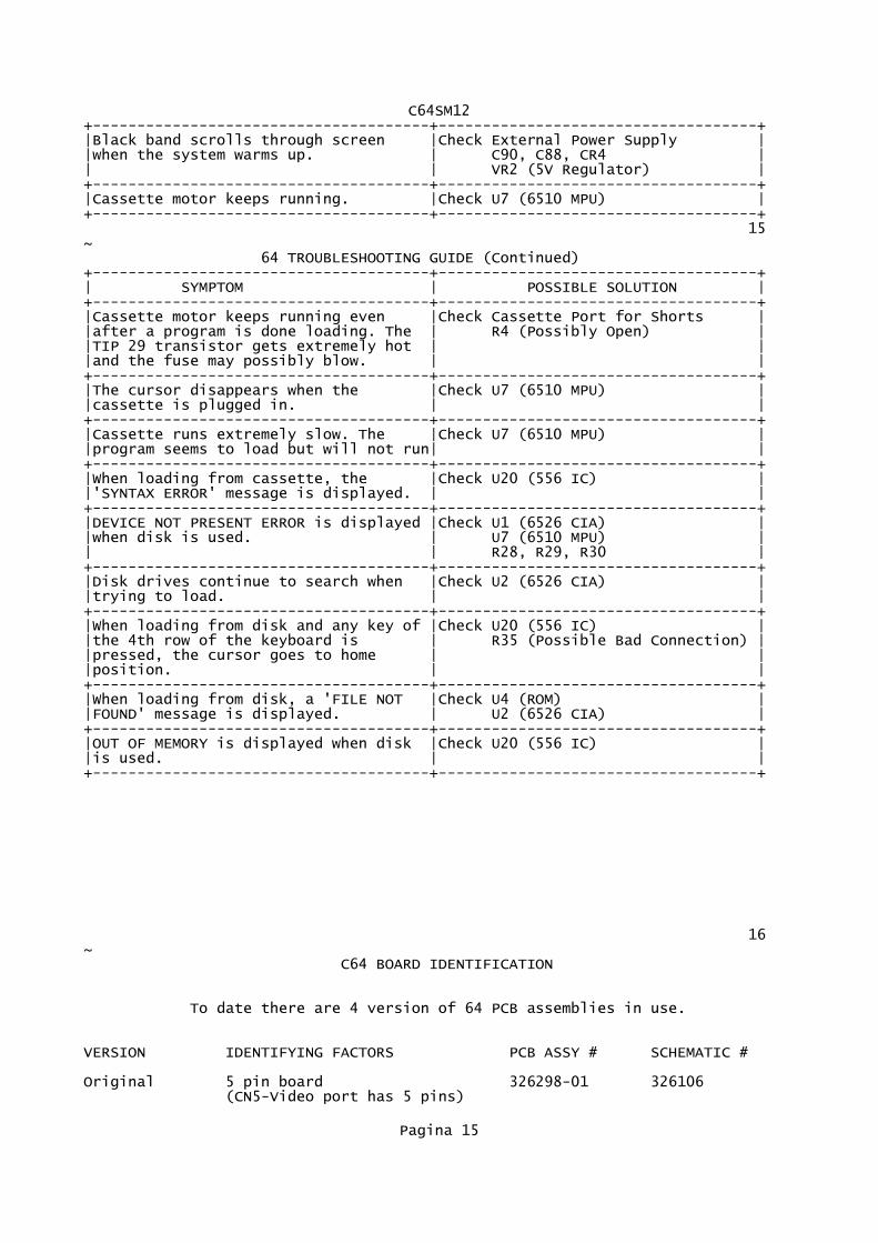
C64SM12+--------------------------------------+------------------------------------+|Black band scrolls through screen |Check External Power Supply ||when the system warms up. | C90, C88, CR4 || | VR2 (5V Regulator) |+--------------------------------------+------------------------------------+|Cassette motor keeps running. |Check U7 (6510 MPU) |+--------------------------------------+------------------------------------+ 15~ 64 TROUBLESHOOTING GUIDE (Continued)+--------------------------------------+------------------------------------+| SYMPTOM | POSSIBLE SOLUTION |+--------------------------------------+------------------------------------+|Cassette motor keeps running even |Check Cassette Port for Shorts ||after a program is done loading. The | R4 (Possibly Open) ||TIP 29 transistor gets extremely hot | ||and the fuse may possibly blow. | |+--------------------------------------+------------------------------------+|The cursor disappears when the |Check U7 (6510 MPU) ||cassette is plugged in. | |+--------------------------------------+------------------------------------+|Cassette runs extremely slow. The |Check U7 (6510 MPU) ||program seems to load but will not run| |+--------------------------------------+------------------------------------+|When loading from cassette, the |Check U20 (556 IC) ||'SYNTAX ERROR' message is displayed. | |+--------------------------------------+------------------------------------+|DEVICE NOT PRESENT ERROR is displayed |Check U1 (6526 CIA) ||when disk is used. | U7 (6510 MPU) || | R28, R29, R30 |+--------------------------------------+------------------------------------+|Disk drives continue to search when |Check U2 (6526 CIA) ||trying to load. | |+--------------------------------------+------------------------------------+|When loading from disk and any key of |Check U20 (556 IC) ||the 4th row of the keyboard is | R35 (Possible Bad Connection) ||pressed, the cursor goes to home | ||position. | |+--------------------------------------+------------------------------------+|When loading from disk, a 'FILE NOT |Check U4 (ROM) ||FOUND' message is displayed. | U2 (6526 CIA) |+--------------------------------------+------------------------------------+|OUT OF MEMORY is displayed when disk |Check U20 (556 IC) ||is used. | |+--------------------------------------+------------------------------------+
16~ C64 BOARD IDENTIFICATION
To date there are 4 version of 64 PCB assemblies in use.
VERSION IDENTIFYING FACTORS PCB ASSY # SCHEMATIC #
Original 5 pin board 326298-01 326106 (CN5-Video port has 5 pins)
Pagina 15
C64SM12A (CR) 8 pin board 250407-04 251138 (CN5-Video port has 8 pins)
B 8 pin board 250425 251469 (Reduced oscillator circuit)
B-2 8 pin board 250441-01* 251469
- These boards are interchangeable with casework, keyboard, etc.; however, care must be taken to provide the customer with a unit that is compatible with their monitor and cable.
- When component level repairs are necessary, be certain to acquire the appropriate part for the board you are repairing. Most modulators are different, as are many of the components.
* The 4th version of 64 board was recently developed and only a few may bein the field. It is termed the 64B-2. All circuits remain the same as the64B (Schematic 251469) with a few component location changes:
1) Resistors 28, 29, 30, 36, 48 were reduced to Resistor Pack RP5.
2) Diodes CR100-105 are no longer piggybacked. Their new locations are CR9, 12-16.
17~ BOARD LAYOUT #326298-01
[Figure: Board Layout #326298-01]
Pagina 16

C64SM12
18~ PARTS LIST - PCB ASSEMBLY #326298 C - Indicates Commodore Stocked Part Numbers
INTEGRATED CIRCUITSU1,U2 6526 CIA C 906108-01U3 2364 Basic ROM C 901226-01U4 2364 Kernal ROM C 901227-03U5 2364 Char ROM C 901225-01U6 2114L-30 RAM 901453-01U7 6510 uProcessor C 906107-01U8 7406 901522-06U9-U12 4164 (200 nS) 901505-01U13 74LS257 901521-57U14 74LS258 901521-58U15 74LS139 901521-18U16 4066 901502-01U17 82S100 PLA C 906114-01U18 6581 SID C 906112-01U19 6567 VIC II C 906109-04U20 LM556 901523-03U21-U24 4161 (200 nS) 901505-01U25 74LS257 901521-57U26 74LS373 901521-29U27 74LS08 901521-03U28 4066 901502-01U29 74LS74 901521-06U30 74LS193 901521-26U31 74LS629 901521-68U32 MC4044 906128-01 TRANSISTORSQ1 2N4401 902652-01Q2 2N3904 902658-01Q3 TIP29 B 902653-01Q4-8 2N2222 902686-01 DIODESCR1 2.7V Zener IN4371CR2 7.5V Zener IN755CR3 IN914CR4 Bridge, Varo VMO8 906129-01CR5,6 Rectifier IN4001 RESISTORS - All values are in ohms- 1/4W, 5%, unless noted otherwise.R1 3.3K R7 10KR2 1.5K R8 390R3 10K R9 75R4 1K R10 120R5 560 R11 120~R6 1K R13 1K RESISTORS (continued)R14 100 R30 1K
Pagina 17

C64SM12R16 1K R31 180R17 1.2K R33 47KR19 15K R34 47KR20 6.8K R35 470KR21 4.7K R37 2.7KR22 1.5K R38 1KR23 1K R39 390R24 3.3K R41 1MR25 Pot 1K R43 3.3KR26 75 R44 3.3KR27 Pot 2K R45 3.3KR28 1K R46 2KR29 1K R51 1.5KNOTE: The input video line requires a 470 ohm, 1/4 watt, resistor soldered to ground.
RESISTOR PACKSRP1,2 33, 8 Pin (Bourne No. 430BR-102-330)RP3 33K, 8 Pin (Bourne No. 430BR-101-332)RP4 3.3K, 10 Pin CAPACITORSC1-3 Ceramic .1 uF, 50VC4-7 Ceramic .47 uF, 50V, 20%C8 Electrolytic 10 uF, 25V, +50%, -10%C9 Ceramic .47 uF, 50V, 20%C10-11 Ceramic 470 pF, 50VC12-15 Electrolytic 10 uF, 25V, +50%, -10%C16 Ceramic .1 uF, 50VC17 Electrolytic 10 uF, 25V, +50%, -10%C18 Ceramic .1 uF, 50VC19 Electrolytic 2200 uF, 16VC20,21 Film .22 uF, 100V, 20%C22 Ceramic .1 uF, 50VC23 Ceramic 360 pF, 50VC24 Electrolytic 10 uF, 25V, +50%, -10%C25-28 Ceramic .22 uF, 50VC29 Ceramic .47 uF, 50V, 20%C30,31,32 Ceramic .1 uF, 50VC33 Ceramic .47 uF, 50V, 20%C34 Electrolytic 10 uF, 25V, +50%, -10%C35 Ceramic .1 uF, 50VC36 Ceramic 20 pF, 50VC37 Ceramic 1000 pF, 50V 19~ PARTS LIST - PCB ASSEMBLY #326298 (Continued) C - Indicates Commodore Stocked Part Numbers
CAPACITORS (Continued)C38 Ceramic 51 uF, 50VC39 Ceramic .1 uF, 50VC40-43 Ceramic .22 uF, 25V, +50%, -10%C44 Ceramic .47 uF, 50V, 20%C45,46,47 Ceramic .1 uF, 50VC48 Ceramic 1800 uF, 50VC49 Ceramic 470 pF, 50VC50 Ceramic .22 uF, 50VC51 Ceramic .47 uF, 50V, 20%C52,53 Ceramic 470 pF, 50VC54 Ceramic .22 uF, 50VC55 Ceramic .1 uF, 50VC56 Ceramic .1 uF, 50VC57 Electrolytic 10 uF, 25V, +50%, -10%C58 Ceramic .1 uF, 50VC59 Ceramic .22 uF, 50VC60,61 Ceramic .47 uF, 50V, 20%C62 Electrolytic 10 uF, 25V, +50%, -10%C63 Ceramic .47 uF, 50V, 20%
Pagina 18

C64SM12C64,65 Electrolytic 10 uF, 25V, +50%, -10%C66,67 Ceramic .47 uF, 50V, 20%C68 Ceramic .1 uF, 50VC69C70 Mica 10 pF, 500V, 5%C71 Ceramic .1 uF, 50VC72 Ceramic 220 pF, 50VC73 Ceramic 150 pF, 50VC74 Ceramic .1 uF, 50VC77 Ceramic .1 uF, 50VC78 Ceramic 220 pF, 50VC79 Ceramic 510 pF, 50VC80 Ceramic 51 pF, 50VC81 Ceramic 20 pF, 50VC82 Ceramic .1 uF, 50VC83 Mica .33 pF, 500V, 5%C84 Ceramic .1 uF, 50VC85 Ceramic .47 uF, 50V, 20%C86 Mica 39 pF, 500V, 5%C87 Ceramic .1 uF, 50VC88 Electrolytic 470 uF, 50VC89 Ceramic .1 uF, 50VC90 Electrolytic 470 uF, 50VC91 Electrolytic 100 uF, 16V~C92 Ceramic .22 uF, 50VC93 Ceramic 1800 uF, 50V
CAPACITORS (Continued)C94 Electrolytic 10 uF, 25V, +50%, -10%C95,96 Ceramic .1 uF, 50VC97 Ceramic .22 uF, 25VC98,99 Ceramic .1 uF, 50VC100 Ceramic .22 uF, 25VC101 Ceramic .1 uF, 50VC102 Electrolytic 10 uF, 25V, +50%, -10%C103 Ceramic .1 uF, 50VC105 Ceramic .1 uF, 50V
CONNECTORSCN1 Header Assy 20 Pin 903331-20CN4 6 Pin Din C 903361-01CN5 5 Pin Din C 903362-01CN6 44 Pin Card Edge C 906100-02CN7 7 Pin Din C 906130-01CN8,9 Plug Assy, 8 Pin Rt. Angle C 906126-01CN10 Header Assy, 3 Pin
MISCELLANEOUSL1,2 Coil Inductor 2.2 uH 901151-17L3 Coil Inductor 3.0 uH 901151-21L4 Filter Line Assy C 906127-01L5 Coil Inductor 1.2 uH 901152-01Y1 Crystal 14.31818 MHz C 900558-01SW1 Rocker Switch DPDT C 904500-01VR1 Voltage Regulator MC7812CTVR2 Voltage Regulator MC7805CTM1 Modulator C 326130-01F1 Fuse, Normal Blo, 250V, 1.5AFB1-23 Ferrite Bread 903025-01 Connector Panel (ON, OFF, Joystick) 326299-01 Catridge Guide 326116-01 Shield Box C 326265-01 Shield Cap C 326267-01
Pagina 19
C64SM12
20~ SCHEMATIC #326106 SHEET 1 OF 2
[Figure: Schematic #326106 sheet 1 of 2]
21~ SCHEMATIC #326106 SHEET 2 OF 2
[Figure: Schematic #326106 sheet 2 of 2]
Pagina 20

C64SM12
22~ BOARD LAYOUT #250407-04
[Figure: Board Layout #250407-04]
Pagina 21

C64SM12
23~ PARTS LIST - PCB ASSEMBLY #250407-04 C - Indicates Commodore Stocked Part Numbers
INTEGRATED CIRCUITSU1,U2 6526 CIA C 906108-01U3 2364 Basic ROM C 901226-01U4 2364 Kernal ROM C 901227-03U5 2364 Char ROM C 901225-01U6 2114L-30 RAM 901453-01U7 6510 uProcessor C 906107-01U8 7406 901522-06 sub: 7416 901522-14U9-U12 4164 (200 nS) 901505-01U13 74LS257 901521-57U14 74LS258 901521-58U15 74LS139 901521-18U16 4066 901502-01U17 82S100 PLA C 906114-01U18 6581 SID C 906112-01U19 6567 VIC II C 906109-04U20 LM556 901523-03U21-U24 4161 (200 nS) 901505-01U25 74LS257 901521-57U26 74LS373 901521-29U27 74LS08 901521-03U28 4066 901502-01U29 74LS74 901521-06U30 74LS193 901521-26U31 74LS629 901521-68U32 MC4044 906128-01 TRANSISTORSQ1,2 2SC1815 C 902693-01Q3 TIP29 A 902653-01Q7,8 2SC1815 C 902693-01 DIODESCR1 2.7V Zener IN4371 906103-02CR2 7.5V Zener IN755 900941-01CR4 Bridge S2VB10 C 251026-01 DBA20B C 251026-02 DBA20C C 251026-03CR5,6 Rectifier IN4001 900750-01 RESISTORS - All values are in ohms- 1/4W, 5%, unless noted otherwise.R1 3.3K R6 1KR2 1.5K R7 10KR3 10K R16 1KR4 1K R17 2.7K~R5 560 R19 15K RESISTORS (continued)R26 75 R39 390R27 Pot 2K R41 1MR28 1K R42 82R29 1K R43 3.3KR30 1K R44 3.3K
Pagina 22
C64SM12R31 180 R45 3.3KR33 47K R50 1MR34 47K R51 1.5KR35 470K R52 300R36 1K R53 390R37 2.7K R100 1KR38 1K R101 22K RESISTOR PACKSRP1,2 33, 8 Pin (Bourne No. 430BR-102-330)RP3 33K, 8 Pin (Bourne No. 430BR-101-332)RP4 3.3K, 10 Pin CAPACITORSC1-7 Ceramic .1 uF, 25VC8 Electrolytic 10 uF, 25V, +50%, -10%C9 Ceramic .1 uF, 25VC10,11 Ceramic 470 pF, 50VC12 Ceramic .1 uF, 25VC13,14,15 Electrolytic 10 uF, 25V, +50%, -10%C16 Ceramic .1 uF, 25VC17 Electrolytic 10 uF, 25V, +50%, -10%C18 Ceramic .1 uF, 25VC19 Electrolytic 2200 uF, 16VC20,21 Film .22 uF, 100V, 20%C22 Ceramic .1 uF, 25VC23 Ceramic 360 pF, 50VC24 Electrolytic 10 uF, 25V, +50%, -10%C25-33 Ceramic .1 uF, 25VC34 Electrolytic 10 uF, 25V, +50%, -10%C35 Ceramic .1 uF, 50VC36 Ceramic 20 pF, 50V, 5% SLC37 Ceramic 1000 pF, 50V, 10% BC38 Ceramic 51 uF, 50V, 5% SLC39-47 Ceramic .1 uF, 25VC48 Ceramic 1800 pF, 50V, 10% BC49-54 Ceramic .1 uF, 25VC55 Ceramic .1 uF, 50VC56 Ceramic .1 uF, 25VC57 Electrolytic 10 uF, 25V, +50%, -10%C58 Ceramic .1 uF, 50V 24~ PARTS LIST - PCB ASSEMBLY #250407-04 (Continued) C - Indicates Commodore Stocked Part Numbers
CAPACITORS (Continued)C59,60 Ceramic .1 uF, 25VC62,65 Electrolytic 10 uF, 25V, +50%, -10%C66,67,68 Ceramic .1 uF, 25VC70 Film 16 pF, 5%C74,82 Ceramic .1 uF, 25VC83 Ceramic 82 pF, 5%C84 Ceramic .1 uF, 25VC85 Ceramic .47 uF, 50V, 10%C88 Electrolytic 1000 uF, 25VC89 Ceramic .1 uF, 25VC90 Electrolytic 470 uF, 50VC91 Electrolytic 100 uF, 16V, +50%, -10%C92 Ceramic .1 uF, 25VC93 Ceramic 1800 pF, 50V, 10% BC94 Electrolytic 10 uF, 25V, +50%, -10%C95,96 Ceramic .1 uF, 25VC97 Ceramic .22 uF, 25VC98,99 Ceramic .1 uF, 25V, +80%, -20%C100 Ceramic .22 uF, 25VC101 Ceramic .1 uF, 50V, +80%, -20%C102 Electrolytic 10 uF, 25V, +50%, -10%C103 Ceramic .1 uF, 25VC104
Pagina 23

C64SM12C105 Ceramic .1 uF, 25VC108 Electrolytic 10 uF, 25V, +50%, -10%C200 Ceramic .1 uF, 25V
CONNECTORSCN1 Header Assy 20 Pin 903331-20CN4 6 Pin Din C 903361-01CN5 8 Pin Din C 325573-01CN6 44 Pin Card Edge C 906100-02CN7 7 Pin Din C 251116-01CN8,9 Plug Assy, 9 Pin MINID C 906126-01CN10 Header Assy, 3 Pin 903332-03
MISCELLANEOUSL2 Coil Inductor 2.2 uH 901151-17L4 Coil Inductor 1.2 uH 325570-01L5 Choke Coil C 325559-02Y1 Crystal 14.31818 MHz C 900558-01SW1 Rocker Switch DPDT C 904500-01VR1 Voltage Regulator MC7812CT 901527-01~VR2 Voltage Regulator MC7805CT 901527-02M1 Modulator C 251080-01F1 Fuse, Normal Blo, 250V, 1.5AFB1-23 Ferrite Bread 903025-01 Connector Panel (ON, OFF, Joystick) 251095-01 Catridge Guide 326116-01 Shield Box C 251023-01 Shield Cap C 251024-01
25
Pagina 24

C64SM12~ MODULATOR SCHEMATIC #251025
[Figure: Modulator schematic #251025]
SCHEMATIC #251138 SHEET 1 OF 2
[Figure: Schematic #251138 sheet 1 of 2]
26~ SCHEMATIC #251138 SHEET 2 OF 2
[Figure: Schematic #251138 sheet 2 of 2]
Pagina 25

C64SM12
27~ BOARD LAYOUT #250425-01
[Figure: Board Layout #250425-01]
Pagina 26

C64SM12
28~ PARTS LIST - PCB ASSEMBLY #250425-01 C - Indicates Commodore Stocked Part Numbers
INTEGRATED CIRCUITSU1,U2 6526 CIA C 906108-01U3 2364 Basic ROM C 901226-01U4 2364 Kernal ROM C 901227-03U5 2364 Char ROM C 901225-01U6 2114L-30 RAM 901453-01U7 6510 uProcessor C 906107-01U8 7406 901522-06 sub: 7416 901522-14U9-U12 4164 (200 nS) 901505-01U13 74LS257 901521-57U14 74LS258 901521-58U15 74LS139 901521-18U16 4066 901502-01U17 82S100 PLA C 906114-01U18 6581 SID C 906112-01U19 6567 VIC II C 906109-04U20 LM556 901523-03U21-U24 4161 (200 nS) 901505-01U25 74LS257 901521-57U26 74LS373 901521-29U27 74LS08 901521-03U28 4066 901502-01U31 7701/8701 C 251527-01 TRANSISTORSQ1 TIP29 A 902653-01Q2-4 2SC1815 C 902693-01 DIODESCR1 2.7V Zener IN4371 906103-02CR2 6.8V Zener IN755CR4 Bridge S2VB10 C 251026-01 sub: DBA20B C 251026-02 sub: DBA20C C 251026-03CR5,6 Rectifier IN4001 900750-01CR9, IN4148 sub:CR12-16 IN914CR100-105 RESISTORS - All values are in ohms- 1/4W, 5%, unless noted otherwise.R1 3.3K R26 3.3KR2 1.5K R31 180R3 10K R33 47KR4 1K R34 47KR5 560 R35 470K~R6 1K R37 2.7KR7 10K R38 1K RESISTORS (continued)R39 390 R50 1MR41 1M R51 1.5KR42 82 R60 100R43 3.3K R100 1KR44 3.3K R101 22KR45 3.3K RESISTOR PACKSRP1,2 33, 8 Pin (Bourne No. 430BR-102-330)
Pagina 27

C64SM12RP3 33K, 8 Pin (Bourne No. 430BR-101-332)RP4 3.3K, 10 PinRP5 1K, 6 Pin CAPACITORSC1-7 Ceramic .1 uF, 25VC9 Ceramic .1 uF, 25VC10,11 Ceramic 470 pF, 50V, 10%C12 Ceramic .1 uF, 25VC13 Electrolytic 10 uF, 25V, +50%, -10%C15 Tantalum 4.7 uF, 16V, 20%C19 Electrolytic 2200 uF, 16VC20 Film .22 uF, 100V, 20%C22 Ceramic .1 uF, 25VC23 Ceramic 360 pF, 50V, 10% sub: 390 pFC24 Electrolytic 22 uF, 25V, +50%, -10%C31,33,34 Ceramic .1 uF, 25VC37 Ceramic 1000 pF, 50V, 10% BC38 Ceramic 51 pF, 50V, 5% SLC39-46 Ceramic .1 uF, 25VC48 Ceramic 1800 pF, 50V, 10% BC50,51,53 Ceramic .1 uF, 25VC59 Ceramic .1 uF, 25VC88 Electrolytic 1000 uF, 25VC90 Electrolytic 470 uF, 50VC91 Electrolytic 100 uF, 16V, +50%, -10%C93 Ceramic 1800 pF, 50V, 10% BC101 Ceramic .1 uF, 50V, +80%, -20%C102 Electrolytic 10 uF, 25V, +50%, -10%C150-152 Ceramic 470 pF, 50V, 10%C153 Ceramic 68 pF, 50V, 5%C154 Ceramic 470 pF, 50V, 10%C200 Ceramic .1 uF, 25VC204 Ceramic 150 pF, 50V, 10%C205 Ceramic 220 pF, 50V, 5%CT1 Trimmer 40 pF 29~ PARTS LIST - PCB ASSEMBLY #250407-04 (Continued) C - Indicates Commodore Stocked Part Numbers
CONNECTORSCN1 Header Assy 20 Pin 903331-20CN4 6 Pin Din C 903361-01CN5 8 Pin Din C 325573-01CN6 44 Pin Card Edge C 906100-02CN7 7 Pin Din C 251116-01CN8,9 Plug Assy, 9 Pin MINID C 251057-01CN10 Header Assy, 3 Pin 903332-03
MISCELLANEOUSL2 Coil Inductor 2.2 uH 901151-17L4 Line Filter Assy C 251701-01L5 Coil Inductor 1.2 uH 901152-01Y1 Crystal 14.31818 MHz C 251707-01SW1 Rocker Switch DPDT C 904500-01VR1 Voltage Regulator MC7812CT 901527-01VR2 Voltage Regulator MC7805CT 901527-02M1 Modulator C 251696-01 Connector Panel (ON, OFF, Joystick) 251095-01 Catridge Guide 326116-01F1 Fuse, Normal Blo, 250V, 1.5A
Pagina 28

C64SM12
30~ MODULATOR SCHEMATIC #251696
[Figure: Modulator schematic #251696]
SCHEMATIC #251469 SHEET 1 OF 2
[Figure: Schematic #251469 sheet 1 of 2]
31~ SCHEMATIC #251469 SHEET 2 OF 2
Pagina 29

C64SM12[Figure: Schematic #251469 sheet 2 of 2]
32~ U1, U2 - 906108-01 6526 COMPLEX INTERFACE ADAPTER (CIA)
PIN 1 VSS Ground connection ASSIGNMENT 2-9 PA0-PA7 Parallel port a signals. +----------+ Bidirectional parallel port. | | 10-17 PB0-PB7 Parallel port b signals. GND-+ 1 40+-CNT Bidirectional parallel port. PA0-+ 2 39+-SP 18 PC Handshake output. A low pulse is PA1-+ 3 38+-RS0 generated after a read or write PA2-+ 4 37+-RS1 on port b. PA3-+ 5 36+-RS2 19 TOD Time od day clock input. PA4-+ 6 35+-RS3 Programmable 50hz or 60hz. PA5-+ 7 34+-_RES 20 VCC 5VDC input. PA6-+ 8 33+-DB0 21 IRQ Interrupt output to microprocessor PA7-+ 9 32+-DB1 input IRQ. PA0-+10 31+-DB2 22 R/W READ/WRITE input from PB1-+11 20+-DB3 microprocessor's R/W output. PB2-+12 29+-DB4 23 CS Chip select input. A low pulse PB3-+13 28+-DB5 will activate CIA. PB4-+14 27+-DB6 24 FLAG Negative edge sensitive interrupt PB5-+15 26+-DB7 input. Can be used as a handshake
Pagina 30

C64SM12 PB6-+16 25+-O2 line for either parallel port. PB7-+17 24+-_FLAG 25 O2 O2 clock input. Connected to PPC-+18 23+-_CS processor common O2 clock. TOD-+19 22+-R/_W 26-33 DB0-DB7 Bidirectional data bus. Connects VCC-+20 21+-_IRQ to processor data bus. | | 34 RES Low active reset input. +----------+ Initializes CIA. 35-38 RS0-RS3 Register select inputs. Used to select all internal registers for communications with the parallel ports, time of day clock and serial port (SP). 39 SP Serial Port bidirectional connection. An internal shift register converts microprocessor parallel data into serial data, and vice versa. 40 CNT Count input. Internal timers can count pulses applied to this input. cAn be used for frequency dependant operations.
~ U18 - 906112-01 6581 SOUND INTERFACE DEVICE (SID)
PIN 1,2, CAP1A,1B ASSIGNMENT 3,4 2A,2B Capacitor filter connections +----------+ 5 RES Reset input. A low pulse | | initializes the SID. CAP-+1A 28+-12V 6 O2 Processor phase 2 clock input. CAP-+1B 27+-A.OUT 7 R/W Processor read/write input. CAP-+2A 26+-EXT IN 8 CS Chip select input. CAP-+2B 25+-5V 9-13 A0-A4 Address lines from processor. _RES-+ 5 24+-POT X 14 GND Dc ground connection. O2-+ 6 23+-POT Y 15-22 D0-D7 Data Bus connections. R/_W-+ 7 22+-D7 23 POT Y Input to a A/D converter used to _CS-+ 8 21+-D6 detect the value of a variable A0-+ 9 20+-D5 resistor. Commonly connected to A1-+10 19+-D4 game paddles. A2-+11 18+-D3 24 POT X Same as POT Y. A3-+12 17+-D2 25 VCC 5VDC. A4-+13 16+-D1 26 EXT IN External audio input. GND-+14 15+-D0 27 A.OUT Audio output. Should be AC coupled | | to audio amp. +----------+ 28 Vdd 12VDC.
Pagina 31

C64SM12
~ U7 - 906107-01 6510 MICROPROCESSOR
PIN 1 O1 Phase 1 clock input. This clock ASSIGNMENT input is used to develop the +----------+ internal overlapping phase 2 | | clock. 1MegHz or 2 MegHz O1-+ 1 40+-_RES speeds. RDY-+ 2 39+-O2 2 RDY Single step operation input. A _IRQ-+ 3 38+-R/_W low applied will cause the _NMI-+ 4 37+-DB0 processor to halt. The current AEC-+ 5 36+-DB1 address line being fetched will VCC-+ 6 35+-DB2 be on the address bus. Can also A0-+ 7 34+-DB3 be used to interface slower A1-+ 8 33+-DB4 devices to the microprocessor. A2-+ 9 32+-DB5 3 IRQ Interrupt request input. When a A3-+10 31+-DB6 low pulse is applied a jump to A4-+11 20+-DB7 a location specified by the A5-+12 29+-P0 contents of FFFE and FFFF will A6-+13 28+-P1 occur to service the interrupt, A7-+14 27+-P2 if the interrupt mask flag is A8-+15 26+-P3 not set. This is a maskable A9-+16 25+-P4 interrupt. A10-+17 24+-P5 4 NMI Non-maskable interrupt input. A A11-+18 23+-A15 low transition will cause a A12-+19 22+-A14 jump to a location specified by A13-+20 21+-GND FFFA and FFFB to a subroutine | | which will service the +----------+ interrupt. 5 AEC Address enable control input. A low applied to will cause the address bus to enter hi impedance state, so other devices can control the address bus. 6 VCC 5VDC input. 7-20 A0-A15 Address bus outputs. 22,23 Unidirectional bus used to address memory and I/O devices. The address bus can be disabled by controlling the AEC input. 21 GND Dc ground connection. 24-29 P0-P5 I/O bidirectional port. This port can be controlled via memory locations 0000 and 0001. 0001 = Output register 0000 = Data direction register~ 30-37 DB0-DB7 Bidirectional data bus. This is the bus that passes the data to or from any I/O device or memory. 38 R/W Read/Write output. The processor generates a low level when writing, and a high level when reading. This signal is usually decoded for read or write operations to memory or I/O. 39 O2 Phase 2 output. The processor generates this clock signal from the phase 1 clock applied. The two clock signals are 180
Pagina 32

C64SM12 degrees out of the phase. The phase 2 clock is used in decoding I/O and memory on the positive half cycle. 40 RES Reset input interrupt. A low pulse causes a jump to a subroutine specified by FFFC and FFFD, which will initialize the all processor controlled devices. This occurs during a power up sequence. ----------------------------------------- PIN ASSIGNMENT +----------+ | | PE+ -+ 1 28+-VCC U17 - 906114-01 I7-+ 2 27+-I8 PROGRAMMABLE I6-+ 3 26+-I9 LOGIC ARRAY (PLA) I5-+ 4 25+-I10 I4-+ 5 24+-I11 I3-+ 6 23+-I12 I2-+ 7 22+-I13 I1-+ 8 21+-I14 I0-+ 9 20+-I15 F7-+10 19+-CE F6-+11 18+-F0 F5-+12 17+-F1 F4-+13 16+-F2 GND-+14 15+-F3 | | +----------+~ U19 - 906109-01 6567 VIDEO INTERFACE CHIP II (VIC II)
PIN ASSIGNMENT +----------+ | | DB6-+ 1 40+-VCC DB5-+ 2 39+-DB7 DB4-+ 3 38+-DB8 DB3-+ 4 37+-DB9 DB2-+ 5 36+-DB10 DB1-+ 6 35+-DB11 DB0-+ 7 34+-A10 _IRQ-+ 8 33+-A9 LP-+ 9 32+-A8 _CS-+10 31+-A7 R/_W-+11 20+-A6 ("1") BA-+12 29+-A5 VDD-+13 28+-A4 COLOR-+14 27+-A3 SYNC/LUM-+15 26+-A2 AEC-+16 25+-A1 PH0-+17 24+-A0 _RAS-+18 23+-A11 _CAS-+19 22+-PHIN VSS-+20 21+-PHCL | | +----------+ MULTIPLEXED ADDRESSES IN PARENTHESES
1-7/39 DB0-DB7 Processor data bus connections. Bidirectional data.
Pagina 33

C64SM12 8 IRQ Interrupt output. Generates a interrupt signal to the processor indicating service is needed. The light pen input can be acknowledged thru use of this interrupt. 10 CS Chip select input. A low signal selects the VIC II. 11 R/W Processor read/write connection. 12 BA Bus available output. A low pulse output indicates the VIC II chip wants control of the processor network to process faster video operations that the system clock can handle. 13 VDD 12VDC input. 14 COLOR Output contains chrominance, color reference burst, and color of display data.~ 15 SYNC/ Output containing video, horizontal and vertical sync, LUM and luminance information. 16 AEC Address enable output. This is usually connected to the processor AEC input controlling the address bus. AEC = 0 processor address bus disabled, refresh ram. AEC = 1 processor address bus enabled. This allows transparent system operations. 17 PH0 Phase 0 output. Generated from the phase in signal. 18 RAS Row address strobe output. Selects proper row when addressing dynamic ram for read/write operations or refresh. 19 CAS Column address strobe output. Selects proper column when addressing dynamic memory for read or write operation. 20 VSS Ground connection. 21 PHCL Color clock, 14.31818 MHZ NTSC. 22 PHIN Clock input. Determines the dot transfer rate to the display. 23-24 A0-A13 Dual function address bus. During a microprocessor read or write operation (AEC = 1), A0 thru A5 are inputs used to address 47 internal registers. When AEC = 0 = O2 is low, then A0 thru A13 are outputs used to refresh dynamic memory. 35-38 D8-D11 Data bus extension. Color display memory data. A8-A11 Address bus extension. Color display memory addressing. 40 VCC 5VDC input.
~ U9 -12, U21 - 24 64K DYNAMIC RAM 901505-01
PIN CONFIGURATION +----------+
Pagina 34

C64SM12 | | NC-+ 1 16+-VSS DIN-+ 2 15+-_CAS _WE-+ 3 14+-DOUT _RAS-+ 4 13+-A6 A0-+ 5 12+-A3 A2-+ 6 11+-A4 A1-+ 7 10+-A5 VCC-+ 8 9+-A7 | | +----------+
+------------+------------+------------+--------+--------+--------+---------+ |COMMODORE |APPROVED |VENDOR |ACCESS | | POWER | |PART |SOURCE |PART |TIME |CYCLES |ACTIVE |STANDBY | |NUMBER |OF SUPPLY |NUMBER |(ns) |(ns) |(MW) |(MAX)(MW)| +------------+------------+------------+--------+--------+--------+---------+ |901505-01 |HITACHI |HM4864-3 |200 |335 |330 |20 | |901505-01 |NEC |uPD4164-2 |200 |375 |250 |28 | |901505-01 |MITSUBISHI |M5K416NS-20 |200 |330 |275 |28 | |901505-01 |MOSTEK |MK4564N-20 |200 |345 |300 |22 | |901505-01 |OKI |MSM3764-20 |200 |330 |248 |23 | |901505-01 |HITACHI |HM4864P-3 |200 |335 |330 |20 | |901505-01 |MATSUSHITA |MN4164P-20 |200 |330 |275 |27.5 | | |(PANASONIC) | | | | | | |901505-01 |SIEMENS |HYB4164-3 |200 |330 |150 |20 | |901505-01 |SHARP |LH2164-Z1 |200 |330 |248 |28 | |901505-01 |HITACHI |HM4864AP-3 |200 |330 |242 |20 | |901505-01 |TOSHIBA |TMM4164AP-20|200 |330 |275 |22 | +------------+------------+------------+--------+--------+--------+---------+
[Figure: DRAM functional diagram]
33
Pagina 35