commercial vcsels and vcsel arrays designed for fdr (14 ... · commercial vcsels and vcsel arrays...
TRANSCRIPT
Commercial VCSELs and VCSEL arrays designed for FDR (14 Gbps) optical links
Roger King*, Steffan Intemann, Stefan Wabra
Philips Technologie GmbH U-L-M Photonics, Lise-Meitner-Straße 13, D-89081 Ulm, Germany
ABSTRACT
Philips recently released a new VCSEL and photodiode product family for the fast growing FDR InfiniBand™ generation. In this work we review the influence of production process variations on VCSEL characteristics, the FDR VCSEL transmission behavior as well as wear-out reliability characteristics. Data collected during an initial 15 wafers pilot production batch verify that FDR VCSEL manufacturing reached mature volume production level. The VCSEL for the next EDR (26Gbps) InfiniBand™ generation is currently being developed at Philips. The paper presents characteristics of the first EDR VCSEL iteration.
Keywords: VCSEL, VCSEL array, FDR, active optical cable
1. INTRODUCTION
High speed I/O fabric is still often based on electrical interconnects. To push the copper interconnects to higher data rates, equalization techniques as well as low loss cables and better connectors have been implemented. But these improvements tend to not follow the market trends. Equalization consumes power, low loss cables are more bulky and make cables supporting wide interfaces very difficult. As a consequence optical cables are becoming more and more common place in high speed I/O fabric and optical buses1. Optical cables offer reduced power consumption and size as well as well long interconnection distances. For example 12 channels wide interfaces are straightforward.
In order to compete with their electrical counterparts optical interconnects must meet basic I/O fabric requirements. Bit error rates shall be 10-18 or better. Longevity of more than 10 years at 0-to-70°C operating temperatures is expected. The optoelectronic technology platform must be able to follow roadmaps like e.g. the IBTA‘s InfiniBand™ roadmap2.
Directly modulated VCSELs are the most attractive light source for optical interconnects due to low cost, low power consumption and ease of integration. Extensive effort has been put in demonstrating that direct modulation line rates of up to 40 Gbps are possible 3,4,5.
VCSELs specifically designed for 14 Gbps FDR lane rates and now being deployed in FDR optical cables will be introduced and discussed. The technology is based upon the established platform of 10 Gbps VCSELs and thus taking loan from a huge database of technological and production experience as well as reliability data. In addition to device performance and reliability data particular attention is paid to link performance parameters. Activities towards 26 Gbps EDR lane rates and preliminary data on device performance will be presented as an outlook to the next evolution in high speed data transmission by VCSELs.
*[email protected]; phone +49 731 550194-020; fax +49 731 550194-026; www.ulm-photonics.de
Invited Paper
Vertical-Cavity Surface-Emitting Lasers XVI, edited by Chun Lei, Kent D. Choquette, Proc. of SPIE Vol. 8276, 82760G · © 2012 SPIE · CCC code: 0277-786X/12/$18 · doi: 10.1117/12.908033
Proc. of SPIE Vol. 8276 82760G-1

2. FDR VCSEL FABRICATION AND CHARACTERISTICS
2.1 Pilot production run
The pilot run workflow starting with 15 epitaxial-grown wafers over to 570 kpcs screened FDR VCSELs till qualified singulated dies is shown in Fig. 1. The epitaxial-grown wafers are taken from four different epi campaigns.
One of the key control parameter is the Fabry-Perot (FP) cavity resonance wavelength which is measured directly after growing the epitaxial layers. Optical gain and doping profiles are checked on calibration wafers. More feedback to epitaxial growth is derived from quality checks during processing, like spatially resolved reflectance measurements, TLM measurements, and temperature dependent threshold current characteristics.
Beside the Fabry-Perot cavity resonance wavelength the second most important device parameter to be tightly controlled is the current aperture diameter. Philips’ VCSEL platform is based on mesa etching and subsequently laterally oxidized current apertures6 where for the FDR VCSEL we have chosen a 7 µm aperture diameter. The frontend steps include mesa etching, oxidation, electrical passivation and device planarization, contact as well as bondpad deposition.
Each wafer from the fabrication line is going through a wafer-level screening procedure where VCSELs with conspicuous and out-of specification characteristics are marked as “bad”. During the pilot run less then 20% of the possible good dies have been sorted out. The screening procedure is based on wafer mapping data like threshold current (Ith), slope efficiency (SE), average output power (Pavg), optical modulation amplitude (OMA), voltage drop (U), differential resistance (Rdiff), center wavelength (CWL), spectral width (RMS) and many more both for 25°C and 85°C wafer backside temperature.
After wafer dicing the singulated dies undergo an automatic optical inspection procedure where again abnormal and out-of specification dies are marked as “bad”. On sample basis farfield angle, equivalent circuit model (ECM) parameters, small signal transfer function resonance frequency (fr) and damping factor (γ), eye mask margin, time-to-failure at [6 mA, 170°C] and [6 mA, 85°C, 85% relative humidity] conditions are tested.
Philips provides single channel, 1x4 and 1x12 VCSEL and PD arrays for 14 Gbps lane rate applications. The 300 µm x 1000 µm 1x4 array design with 250 µm channel spacing is shown in Fig. 2 both for the FDR VCSEL and for informative purposes also for the matching FDR PD chip. Anode and cathode pads with a diameter of 70 µm are on the top-side.
Figure 2. Top view of an flip-chip 1x4 top-emitting VCSEL (left) and top-receiving photodiode (right) array die.
Epitaxy(15 Wfr out)
FP resonancewavelength
Frontend Screening(570k out)
Dicing
Opt Insp
Lot
Quali
Activediameter
Ith, SEPavg, OMAU, RdiffCWL, RMS� 100% testing
Farfield angleECM-parameterfr, γEye diagramALT (170°C)THB (85°C, 85%rh)� On sampe basis
Epitaxy(15 Wfr out)
FP resonancewavelength
Frontend Screening(570k out)
Dicing
Opt Insp
Lot
Quali
Activediameter
Ith, SEPavg, OMAU, RdiffCWL, RMS� 100% testing
Farfield angleECM-parameterfr, γEye diagramALT (170°C)THB (85°C, 85%rh)� On sampe basis
Figure 1. Pilot production workflow starting with epitaxial-grown wafers till qualified singulated dies
Proc. of SPIE Vol. 8276 82760G-2

2.2 Static characteristics
The following Figs. 3 to 7 show cumulative parameter histograms for the VCSELs that passed the screening procedure described in the previous section. Philips recommends to drive the FDR VCSEL between 3 mA laser current in the low state and 9 mA laser current in the high state. The parameters in the diagrams of Figs. 3 to 7 are matched to the recommended drive conditions. For the purpose of reference the cumulative distribution function for the respective standard Gaussian distribution is plotted in diagrams below, too.
Fig. 3 depicts the cumulative histogram for the average output power and for the optical modulation amplitude. The average output power does not exceed 2.4 mW at 25°C chip backside temperature (Tchip). The smallest optical modulation amplitude of 1.1 mW is recorded at Tchip = 85°C. As can be seen from Fig. 4 the differential resistance is matched to 50 Ohm and the voltage drop at 6 mA is below 2 V.
Fig. 5 shows cumulative histograms for threshold current and slope efficiency. The typical threshold current at room temperature is 0.7 mA and does not exceed 1.4 mA at 85°C.
FDR optical cables typically require that the center wavelength stays within 840 nm and 860 nm and the spectral width below 0.65 nm. As can be seen from Fig. 6 both requirements are met.
Because it significantly limits static, dynamic and reliability performance it is important to keep current induced self-heating in the VCSEL as low as possible. Fig. 7 shows that the VCSEL dissipates power in the order of 10 mW. With the empirically verified formula on the right hand (+/- 2°C compared to Ti estimates by measuring wavelength shifts), self-heating is found to be typically +34°C at 85°C chip backside temperature and 6 mA laser current.
0%
20%
40%
60%
80%
100%
0.5 1.0 1.5 2.0 2.5 3.0
Output power at 6mA, Pi6 [mW]
CD
F
25°C
55°C
85°C
0%
20%
40%
60%
80%
100%
1.0 1.5 2.0 2.5 3.0
Opt mod amplitude at 6mA, OMAi6 [mW]
CD
F
25°C
55°C
85°C
Figure 3. Cumulative histograms for the optical output power at 6 mA (left) and optical modulation amplitude at 3-9 mA (right) drive current. Sample mean for Pi6 and OMAi6 is [2.1, 1.8, 1.4] and [2.2, 1.9, 1.5] mW at Tchip = [25, 55, 85]°C, respectively.
0%
20%
40%
60%
80%
100%
1.70 1.75 1.80 1.85 1.90 1.95 2.00
Voltage drop at 6mA, Ui6 [V]
CD
F 25°C55°C
85°C
0%
20%
40%
60%
80%
100%
30 35 40 45 50 55 60 65 70
Diff resistance at 6mA, Rdiffi6 [Ohm]
CD
F
25°C
55°C
85°C
Figure 4. Cumulative histograms for the voltage drop (left) and differential resistance (right) at 6 mA drive current. Sample mean for Ui6 and Rdiffi6 is [1.86, 1.82, 1.79] V and [53, 50, 48] Ohm at Tchip = [25, 55, 85]°C, respectively.
Proc. of SPIE Vol. 8276 82760G-3

0%
20%
40%
60%
80%
100%
0.2 0.4 0.6 0.8 1.0 1.2 1.4
Threshold current, Ith [mA]
CD
F
25°C
55°C
85°C
0%
20%
40%
60%
80%
100%
0.1 0.2 0.3 0.4 0.5 0.6
Slope efficiency, SE [W/A]
CD
F
25°C
55°C
85°C
Figure 5. Cumulative histograms for the threshold current (left) and slope efficiency (right). Sample mean for Ith and SE is [0.6, 0.7, 0.9] mA and [53, 50, 48] Ohm at Tchip = [25, 55, 85]°C, respectively.
0%
20%
40%
60%
80%
100%
840 845 850 855 860
Center wavelength at 6mA, CWLi6 [nm]
CD
F
25°C
55°C
85°C
0%
20%
40%
60%
80%
100%
0.1 0.2 0.3 0.4 0.5 0.6
Spectral width, RMSi6 [nm]
CD
F
25°C
55°C
85°C
Figure 6. Cumulative histograms for the center wavelength (left) and spectral width (right) at 6 mA drive current. Sample mean for CWLi6 and RMSi6 is [849, 851, 853] nm and [0.40, 0.33, 0.28] nm at Tchip = [25, 55, 85]°C, respectively.
0%
20%
40%
60%
80%
100%
8.5 9.0 9.5 10.0 10.5
Dissipated power at 6mA, Pdissi6 [mW]
CD
F
25°C
55°C
85°C
( )
( ) ( ) ( )dTRIPdITT
TddTR
hsthdisshsi
hshsth
,,,
15.27325
15.273µm7mW
K0.3,8.08.0
⋅=
⎟⎠
⎞⎜⎝
⎛
++⋅⎟
⎠⎞⎜
⎝⎛⋅=
Figure 7. Cumulative histograms for the dissipated power (left) and empirically verified formula to calculate the VCSEL internal temperature Ti6 (right). Sample mean for Pdissi6 and Ti at 6 mA is [9.6, 9.6, 9.9] mW and [54, 86, 119]°C at Tchip = Ths = [25, 55, 85]°C, respectively.
Proc. of SPIE Vol. 8276 82760G-4

2.3 Large-signal modulation performance
The role of a VCSEL in an optical cable is to transmit optical signals. Therefore the large-signal modulation behavior of the FDR VCSEL is very important. We performed numerous large-signal modulation measurements on typical and corner type FDR VCSELs from the pilot production run described in section 2.1. Over the entire temperature range from 25°C to 85°C the eyes obtained are nicely open.
Fig. 8 shows typical eye diagrams recorded at 25°C (left) and 85°C (right) heatsink temperature where the PRBS31 signal from the 50 Ohm pattern generator is fed to the VCSEL via a high frequency probe tip. The average VCSEL current and the optical extinction ratio is 6 mA and 4.5 dB, respectively. The lane rate of 13.5 Gbps instead of 14 Gbps is because of limitations in the available pattern generator.
The eye diagram in Fig. 9 is produced with an FDR VCSEL which is wire-bonded to a driver IC (IPVD16G4C from Iptronics A/S) which drives the laser current between 3 mA and 9 mA in the low- and high-state, respectively. A mask margin of 20% is measured at 25°C heatsink temperature.
Figure 8. Eye diagrams at 25°C (left) and 85°C (right) recorded at 13.5 Gbps at 6 mA average laser current and a constant extinction ratio of 4.5 dB. The PRBS31 test pattern comes from a 50 Ohm pattern generator. VCSEL is contacted via HF probe tip.
Figure 9. 13.5 Gbps eye diagram at 25°C which is recorded at Ilow = 3 mA and Ihigh = 9 mA . The VCSEL is mounted on a FDR evaluation board and contacted to the driver IC (IPVD16G4C from IPtronics) via wire-bonding.
2.4 Wear out analysis
In order to study the wear out behavior of the FDR VCSEL we accelerate the aging process by increasing the substrate temperature and derive wear out lifetime predictions by analyzing the time-to-failure (TTF) distribution. The sample set so far includes 105 VCSEL that have passed the screening procedure described in section 2.1 and are randomly picked from 8 different wafers. The devices are continuously operated at 6 mA laser current at 170°C substrate temperature. Once every 24 h the room temperature LIV curve of the devices is recorded. The failure criterion is 2 dB degradation in optical output power relative to optical output power at the beginning of the test.
Proc. of SPIE Vol. 8276 82760G-5
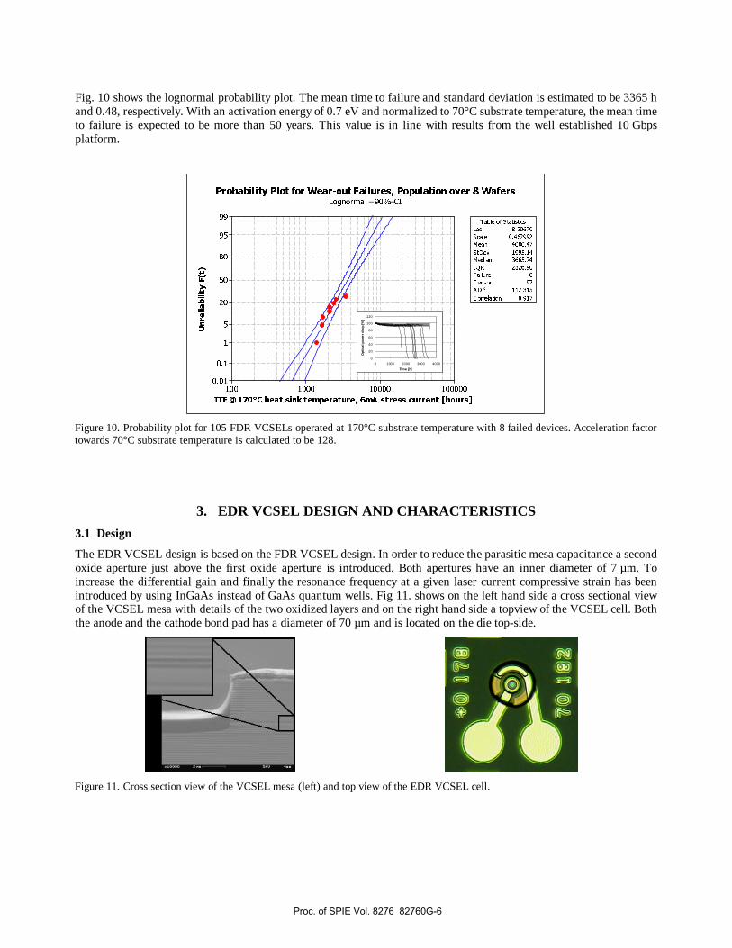
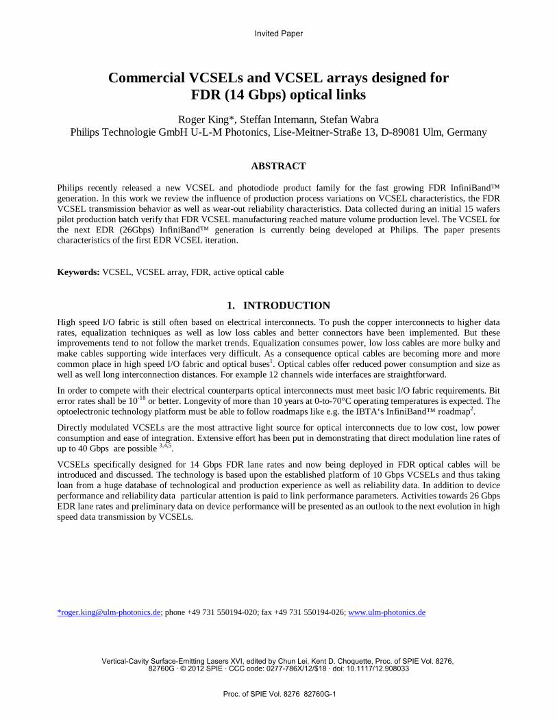
Fig. 10 shows the lognormal probability plot. The mean time to failure and standard deviation is estimated to be 3365 h and 0.48, respectively. With an activation energy of 0.7 eV and normalized to 70°C substrate temperature, the mean time to failure is expected to be more than 50 years. This value is in line with results from the well established 10 Gbps platform.
100000100001000100
99
95
80
50
20
5
1
0.1
0.01
TTF @ 170°C heat sink temperature, 6mA stress current [hours]
Unreliability F(t)
Correlation 0.917
Loc 8.20679
Scale 0.462992
Mean 4080.47
StDev 1995.14
Median 3665.74
IQR 2326.90
Failure 8
Censor 97
AD* 112.315
Table of Statistics
Probability Plot for Wear-out Failures, Population over 8 WafersLognormal - 90%-CI
Figure 10. Probability plot for 105 FDR VCSELs operated at 170°C substrate temperature with 8 failed devices. Acceleration factor towards 70°C substrate temperature is calculated to be 128.
3. EDR VCSEL DESIGN AND CHARACTERISTICS
3.1 Design
The EDR VCSEL design is based on the FDR VCSEL design. In order to reduce the parasitic mesa capacitance a second oxide aperture just above the first oxide aperture is introduced. Both apertures have an inner diameter of 7 µm. To increase the differential gain and finally the resonance frequency at a given laser current compressive strain has been introduced by using InGaAs instead of GaAs quantum wells. Fig 11. shows on the left hand side a cross sectional view of the VCSEL mesa with details of the two oxidized layers and on the right hand side a topview of the VCSEL cell. Both the anode and the cathode bond pad has a diameter of 70 µm and is located on the die top-side.
Figure 11. Cross section view of the VCSEL mesa (left) and top view of the EDR VCSEL cell.
0
20
40
60
80
100
120
0 1000 2000 3000 4000
Time [h]
Op
tica
l po
we
r d
rop
[%]
Proc. of SPIE Vol. 8276 82760G-6

3.2 Static characteristics
Typical LIV curves of the first generation of EDR VCSEL and the optical spectrum at 6 mA laser current are plotted in Fig. 12 on the left and right hand side, respectively. At 25°C the threshold is 0.6 mA and slope efficiency is 0.68 W/A. At 85°C threshold current is increased to 1.1 mA and a slope efficiency reduced to 0.47 W/A. At a typical operating current of 8 mA, the output power at 25°C and 85°C is 4.5 mW and 2.2 mW, respectively
0
0.5
1
1.5
2
2.5
0 2 4 6 8 10 12 14
Current [mA]
Vo
ltag
e [V
]
012345678910
Op
tical
Po
wer
[mW
]
25°C85°C
0
5
10
15
20
25
30
35
40
45
840 842 844 846 848 850
Wavelength [nm]
Po
wer
leve
l [d
B]
Figure 12. LIV curves (left) and optical spectrum at 6 mA (right) of a 7 µm active diameter EDR VCSEL.
3.3 Modulation characteristics
To investigate the large signal modulation a 25 Gbps PRBS7 test signal from a 50 Ohm pattern generator is fed to the VCSEL via a high frequency probe tip. At 25°C substrate temperature, 8 mA average drive current and 4 dB optical extinction ratio a mask margin of 5% is obtained.
Figure 13. Eye diagram at 25°C recorded at 25 Gbps at 8 mA average laser current and a extinction ratio of 4 dB. The PRBS7 test pattern comes from a 50 Ohm pattern generator. The VCSEL is contacted via HF probe tip.
3.4 Analysis of the modulation characteristics
The electrical load behavior of the EDR VCSEL is extracted from S-Parameter measurements and can be described using the distributed equivalent circuit model as listed in Fig 14. It is calculated that the 3 dB bandwidth is currently limited to 17 GHz due to parasitics. A 15% reduction of the mesa capacitance will increase the limit to 24 GHz.
v0 C0 C1 R2
R1L0R0
i2
i1
C2
popt(i2)
Driver Package Parasites E/O
v0 C0 C1 R2
R1L0R0
i2
i1
C2
popt(i2)
Driver Package Parasites E/O
T [°C] Current [mA] R1 [Ohm] C1 [fF] R2 [Ohm] C2 [fF] f3dB [GHz]5 27.9 6 51.4 294 17.210 30.1 6 24.6 416 20.514 31.5 6 14.9 643 19.45 27.9 6 33.9 389 17.210 29.0 6 26.7 624 18.014 29.5 6 10.7 980 17.0
25
85
Figure 14. Equivalent circuit model of the VCSEL (left) and extracted model parameters (right) from load measurements.
Proc. of SPIE Vol. 8276 82760G-7

To understand the electro-optical bandwidth limitations a two pole transfer function to model the conversion process in the quantum well layers is used. The two pole transfer function parameters resonance frequency (fr) and damping factor (γ) are obtained via fitting to S11(f) and S21(f) network analyzer measurements. Resonance frequencies and damping factors for various temperature and current settings are plotted in Fig. 1. At 85°C substrate temperature current induced self-heating in the VCSEL limits the resonance frequency to below 12 GHz and needs to be reduced in the next iteration.
0
5
10
15
20
25
0 1 2 3 4
√( I - Ith ) [√mA]
Res
on
ance
freq
. [G
Hz] 25°C
85°C
Thermalroll over
D = 4.54 GHz/mA-½
D = 6.14 GHz/mA-½
0
5
10
15
20
25
0 1 2 3 4
√( I - Ith ) [√mA]
Res
on
ance
freq
. [G
Hz] 25°C
85°C
Thermalroll over
D = 4.54 GHz/mA-½
D = 6.14 GHz/mA-½
0
50
100
150
200
0 100 200 300 400
fr² [GHz²]
γ
[1/
ns]
25°C85°C
K=0.483 ns
K=0.151 ns
f3dB = 18.6 GHz
0
50
100
150
200
0 100 200 300 400
fr² [GHz²]
γ
[1/
ns]
25°C85°C
K=0.483 ns
K=0.151 ns
f3dB = 18.6 GHz
Figure 16. Resonance frequency as a function of laser current (left) and K-factor diagram (right).
4. CONCLUSION
We have described that FDR VCSEL manufacturing has achieved high yields. Temperature stable, clear and open eye diagrams with an extinction ratio >4dB at FDR lane rates, from 25 to 85 degC substrate temperature under constant drive conditions were obtained with the FDR VCSEL. Mean time to failure normalized to 70°C substrate temperature is expected to be more than 50 years.
The first iteration of 26 Gbps lane rate EDR VCSELs shows clear and open eye diagrams at 25°C with 4 dB optical extinction ratio. Bandwidth limitations in the electro-optical conversion at 85°C need to be addressed in the next iteration.
ACKNOWLEDGEMENTS
Special thanks for all the technical support to all of our colleagues at U-L-M photonics. We gratefully acknowledge the financial support for the 26 Gbps work by Federal Ministry of Education and Research of Germany (BMBF) under the frame work of the project WioNet.
REFERENCES
[1] C. Schow, F. Doany, J. Kash, “Get On The Optical Bus,” IEEE Spectrum, 47, 32-56, (2010). [2] http://www.infinibandta.org/content/pages.php?pg=technology_overview [3] P. Westbergh, J. S. Gustavsson, B. Kögel, A. Haglund, and A. Larsson., “Impact of Photon Lifetime on High-
Speed VCSEL Performance,” IEEE J. Sel. Topics Quantum Electron., 17, 1603–1613, (2011). [4] W. Hofmann, P. Moser, P. Wolf, A. Mutig, M. Kroh, and D. Bimberg, "44 Gb/s VCSEL for optical
interconnects," Proc. OSA/OFC/NFOEC 2011, PDPC5, (2011). [5] Y.-C. Chang and L. A. Coldren, “Efficient, high-data-rate, tapered oxide aperture vertical-cavity surface-
emitting lasers,” IEEE J. Sel. Topics Quantum Electron., 15, 704–715, (2009). [6] D. Wiedenmann*, M. Grabherr, R. Jäger, R. King, “High volume production of single-mode VCSELs”, Proc.
SPIE 6132, 613202-1..12 (2006).
Proc. of SPIE Vol. 8276 82760G-8