com express™ conga-ts77 - contradata 2013.02.08 aem ... • changed the pull up value of wake0#...
TRANSCRIPT

COM Express™ conga-TS773rd Generation Intel® Core™ i7, i5, i3 processor with QM77 PCH or 2nd and 3rd Generation Intel®
Celeron processor with HM76 PCH
User’s Guide
Revision 1.3

Copyright © 2012 congatec AG TS77m13 2/110
Revision HistoryRevision Date (yyyy.mm.dd) Author Changes0.1 2012.07.27 AEM • Preliminary release0.2 2012.10.04 AEM • Added Celeron variants through out the document. Corrected and updated the power consumption tables in section 1.5.1 - 1.5.9.
• Included PEG Gen 3 support in section 4.2.2. • Added statement about the optional use of the PEG interface for connecting a x1, x2, x4, or x8 non-graphic PCI Express device in
section 4.2.2 “PCI Express Graphics (PEG)”. • Deleted the note in sections 4.2.4 “HDMI”, 4.2.5 “DisplayPort” and 7.5 “Boot Strap Signals” which made reference to the application note
AN17_HDMI_DP_Implementation.pdf because the referred application note applies to COM Express Type 2 designs only. • Added note about Watchdog NMI mode not being supported to sections 5.3 “Watchdog” and 9.4.2 “Watchdog Configuration Submenu”. • Added note to “Gigabit Ethernet Signal Descriptions” table in section 7. • Corrected pin B101 signal from 3MOUT to FAN_PWNOUT in section 7.1 table 13 “Miscellaneous Signal Description”. • Deleted the menu bar chipset column and the F7 key option in section 9.2 “Setup Menu and Navigation“. • Deleted the power column in section 9.4 “Advanced Setup“. Updated section 9.4.3.1 “PCI Express Graphics (PEG) Port Submenu” with
new BIOS features. .0.3 2012.12.20 AEM • Added Microsoft Windows 8 support in section 1.2 “ Supported Operating Systems”
• Updated section 4.1.12 “Power Control”.• Corrected the statement that the display port is multiplexed onto the PCI Express Graphics interface of the COM Express connector in
section 4.2.5 “DisplayPort”.• Updated the BIOS description in section 9 “BIOS Setup Description“.
1.0 2013.02.08 AEM • Edited section 4.2.2 “PCI Express Graphics (PEG) and corrected the statement that the additional PEG links cannot be linked with each other.
• Edited section 8.2.1 “LPC Bus”• Official release
1.1 2013.04.23 AEM • Added section 1 “Introduction”. Moved COM Express™ Concept and Options Information to section 1 “Introduction”.• Added SATA Gen 3 support for two SATA ports (SATA 0 and 1) in section 6.1.1 “Serial ATA™ (SATA)”• Added three additional celeron variants in section 1 “Introduction”, section 2.1 “Feature List” and section 2.5 “Power Consumption”. • Added section 5 “Onboard Sensors”. • Added section 12.1 “Supported Flash Devices”.• Changed the Pull up value of WAKE0# signal from 10k to 1k in table 15 “Power and System Management Signal Description”.• Deleted the comment “Connect to CB_RESET#” for express card reset signals in Table 7.• Updated the whole document. Added note in sections 6.2.3 “SDVO”, 6.2.4 “HDMI” and 6.2.5 “DisplayPort”.
1.2 2013.08.21 AEM • Corrected the statement that congatec variants equipped with Intel HM76 PCH do not support USB 3.0 in section 2.1 “Feature List”.• Updated section 2.5 “Power Consumption” and section 3 “Block Diagram”.• Deleted the note in section 6.2.6 “USB 3.0”• Added the “#” sign to the signal “SLEEP” in table 15 “Power and System Management Signal Description” to indicate that this signal is
active with low voltage level.1.3 2014.05.27 AEM • Updated section 3 “Block Diagram” and section 6.25 “DisplayPort (DP)”
• Corrected pins D63 and D64 in section 9.4 “C-D Connector Pinout”.• Updated section 11 “BIOS Setup Description”.

Copyright © 2012 congatec AG TS77m13 3/110
PrefaceThis user’s guide provides information about the components, features, connectors and BIOS Setup menus available on the conga-TS77. It is one of three documents that should be referred to when designing a COM Express™ application. The other reference documents that should be used include the following:
COM Express™ Design GuideCOM Express™ Specification
The links to these documents can be found on the congatec AG website at www.congatec.com
Disclaimer
The information contained within this user’s guide, including but not limited to any product specification, is subject to change without notice.
congatec AG provides no warranty with regard to this user’s guide or any other information contained herein and hereby expressly disclaims any implied warranties of merchantability or fitness for any particular purpose with regard to any of the foregoing. congatec AG assumes no liability for any damages incurred directly or indirectly from any technical or typographical errors or omissions contained herein or for discrepancies between the product and the user’s guide. In no event shall congatec AG be liable for any incidental, consequential, special, or exemplary damages, whether based on tort, contract or otherwise, arising out of or in connection with this user’s guide or any other information contained herein or the use thereof.
Intended Audience
This user’s guide is intended for technically qualified personnel. It is not intended for general audiences.
Lead-Free Designs (RoHS)
All congatec AG designs are created from lead-free components and are completely RoHS compliant.
Electrostatic Sensitive Device
All congatec AG products are electrostatic sensitive devices and are packaged accordingly. Do not open or handle a congatec AG product except at an electrostatic-free workstation. Additionally, do not ship or store congatec AG products near strong electrostatic, electromagnetic, magnetic, or radioactive fields unless the device is contained within its original manufacturer’s packaging. Be aware that failure to comply with these guidelines will void the congatec AG Limited Warranty.

Copyright © 2012 congatec AG TS77m13 4/110
Symbols
The following symbols are used in this user’s guide:
Warning
Warnings indicate conditions that, if not observed, can cause personal injury.
Caution
Cautions warn the user about how to prevent damage to hardware or loss of data.
Note
Notes call attention to important information that should be observed.
Terminology
Term DescriptionGB Gigabyte (1,073,741,824 bytes)GHz Gigahertz (one billion hertz)kB Kilobyte (1024 bytes)MB Megabyte (1,048,576 bytes)Mbit Megabit (1,048,576 bits)kHz Kilohertz (one thousand hertz)MHz Megahertz (one million hertz)TDP Thermal Design PowerPCIe PCI Express DDI Digital Display InterfaceSATA Serial ATAPEG PCI Express GraphicsPCH Platform Controller HubPATA Parallel ATAT.O.M. Top of memory = max. DRAM installedHDA High Definition AudioI/F InterfaceN.C. Not connectedN.A. Not availableTBD To be determined

Copyright © 2012 congatec AG TS77m13 5/110
Trademarks
Product names, logos, brands, and other trademarks featured or referred to within this user’s guide, or the congatec website, are the property of their respective trademark holders. These trademark holders are not affiliated with congatec AG, our products, or our website.
Warranty
congatec AG makes no representation, warranty or guaranty, express or implied regarding the products except its standard form of limited warranty (“Limited Warranty”) per the terms and conditions of the congatec entity, which the product is delivered from. These terms and conditions can be downloaded from www.congatec.com. congatec AG may in its sole discretion modify its Limited Warranty at any time and from time to time.
The products may include software. Use of the software is subject to the terms and conditions set out in the respective owner’s license agreements, which are available at www.congatec.com and/or upon request.
Beginning on the date of shipment to its direct customer and continuing for the published warranty period, congatec AG represents that the products are new and warrants that each product failing to function properly under normal use, due to a defect in materials or workmanship or due to non conformance to the agreed upon specifications, will be repaired or exchanged, at congatec’s option and expense.
Customer will obtain a Return Material Authorization (“RMA”) number from congatec AG prior to returning the non conforming product freight prepaid. congatec AG will pay for transporting the repaired or exchanged product to the customer.
Repaired, replaced or exchanged product will be warranted for the repair warranty period in effect as of the date the repaired, exchanged or replaced product is shipped by congatec, or the remainder of the original warranty, whichever is longer. This Limited Warranty extends to congatec’s direct customer only and is not assignable or transferable.
Except as set forth in writing in the Limited Warranty, congatec makes no performance representations, warranties, or guarantees, either express or implied, oral or written, with respect to the products, including without limitation any implied warranty (a) of merchantability, (b) of fitness for a particular purpose, or (c) arising from course of performance, course of dealing, or usage of trade.
congatec AG shall in no event be liable to the end user for collateral or consequential damages of any kind. congatec shall not otherwise be liable for loss, damage or expense directly or indirectly arising from the use of the product or from any other cause. The sole and exclusive remedy against congatec, whether a claim sound in contract, warranty, tort or any other legal theory, shall be repair or replacement of the product only.
Copyright © 2012 congatec AG TS77m13 6/110
Certification
congatec AG is certified to DIN EN ISO 9001 standard.
Technical Support
congatec AG technicians and engineers are committed to providing the best possible technical support for our customers so that our products can be easily used and implemented. We request that you first visit our website at www.congatec.com for the latest documentation, utilities and drivers, which have been made available to assist you. If you still require assistance after visiting our website then contact our technical support department by email at [email protected]
CERTIFICATION
ISO 9001
TM

Copyright © 2012 congatec AG TS77m13 7/110
Contents1 INTRODUCTION ..................................................................... 10
2 Specifications ........................................................................... 12
2.1 Feature List .............................................................................. 122.2 Supported Operating Systems ................................................. 132.3 Mechanical Dimensions ........................................................... 132.4 Supply Voltage Standard Power .............................................. 142.4.1 Electrical Characteristics .......................................................... 142.4.2 Rise Time ................................................................................. 142.5 Power Consumption ................................................................. 152.5.1 conga-TS77 Intel® Core™ i7-3612QE 2.1 GHz 6MB Cache .. 162.5.2 conga-TS77 Intel® Core™ i7-3555LE 2.5 GHz 4MB Cache .... 162.5.3 conga-TS77 Intel® Core™ i7-3517UE 1.7 GHz 4MB Cache .... 172.5.4 conga-TS77 Intel® Core™ i7-3615QE 2.3 GHz 6MB Cache .. 172.5.5 conga-TS77 Intel® Core™ i5-3610ME 2.7 GHz 3MB Cache ... 172.5.6 conga-TS77 Intel® Core™ i3-3217UE 1.6 GHz 3MB Cache .... 182.5.7 conga-TS77 Intel® Core™ i3-3120ME 2.4 GHz 3MB Cache ... 182.5.8 conga-TS77 Intel® Celeron® 827E 1.4 GHz 1 Core™ 1.5MB
Cache ....................................................................................... 182.5.9 conga-TS77 Intel® Celeron® 847E 1.1 GHz 2 Core™ 2MB Cache
192.5.10 conga-TS77 Intel® Celeron® 1047UE 1.4 GHz 2 Core™ 2MB
Cache ....................................................................................... 192.5.11 conga-TS77 Intel® Celeron® 1020E 2.2 GHz 2 Core™ 2MB Cache
192.5.12 conga-TS77 Intel® Celeron® 927UE 1.5 GHz 1 Core™ 1MB
Cache ....................................................................................... 202.6 Supply Voltage Battery Power ................................................. 202.6.1 CMOS Battery Power Consumption ........................................ 202.7 Environmental Specifications ................................................... 21
3 Block Diagram .......................................................................... 22
4 Heatspreader ........................................................................... 23
4.1 Heatspreader Dimensions ....................................................... 244.2 Heatspreader Thermal Imagery ............................................... 25
5 Onboard Temperature Sensors ................................................ 26
6 Connector Subsystems Rows A, B, C, D ................................. 28
6.1 Primary Connector Rows A and B ............................................ 296.1.1 Serial ATA™ (SATA) ................................................................. 296.1.2 USB 2.0 .................................................................................... 296.1.3 High Definition Audio (HDA) Interface ...................................... 296.1.4 Gigabit Ethernet ...................................................................... 296.1.5 LPC Bus ................................................................................... 306.1.6 I²C Bus Fast Mode ................................................................... 306.1.7 PCI Express™ ......................................................................... 306.1.8 ExpressCard™ ......................................................................... 306.1.9 Graphics Output (VGA/CRT) ................................................... 306.1.10 LCD .......................................................................................... 316.1.11 General Purpose Serial Interface ............................................. 316.1.12 Power Control .......................................................................... 316.1.13 Power Management ................................................................. 346.2 Secondary Connector Rows C and D ...................................... 356.2.1 PCI Express™ ......................................................................... 356.2.2 PCI Express Graphics (PEG) ................................................... 356.2.3 SDVO ....................................................................................... 366.2.4 HDMI ........................................................................................ 366.2.5 DisplayPort (DP) ...................................................................... 376.2.6 USB 3.0 .................................................................................... 37
7 Additional Features .................................................................. 38
7.1 congatec Board Controller (cBC) ............................................. 387.2 Board Information .................................................................... 387.3 Watchdog ................................................................................. 387.4 I2C Bus ..................................................................................... 387.5 Power Loss Control .................................................................. 397.6 Embedded BIOS ...................................................................... 397.6.1 CMOS Backup in Non Volatile Memory ................................... 397.6.2 OEM CMOS Default Settings and OEM BIOS Logo ................ 397.6.3 OEM BIOS Code ...................................................................... 397.6.4 congatec Battery Management Interface ................................. 40
Copyright © 2012 congatec AG TS77m13 8/110
7.6.5 API Support (CGOS/EAPI) ...................................................... 407.7 Security Features ..................................................................... 417.8 Suspend to Ram ...................................................................... 41
8 conga Tech Notes .................................................................... 42
8.1 Intel Turbo Boost 2 ................................................................... 428.2 Intel® Matrix Storage Technology ............................................ 438.2.1 AHCI ........................................................................................ 438.2.2 RAID ........................................................................................ 438.2.3 Intel® Smart Response Technology ......................................... 438.3 Intel® Processor Features ........................................................ 448.3.1 Thermal Monitor and Catastrophic Thermal Protection ........... 448.3.2 Processor Performance Control ............................................... 458.3.3 Intel® 64 .................................................................................... 458.3.4 Intel® Virtualization Technology ................................................ 468.4 Thermal Management .............................................................. 468.5 ACPI Suspend Modes and Resume Events ............................ 488.6 USB 2.0 EHCI Host Controller Support ................................... 49
9 Signal Descriptions and Pinout Tables ..................................... 50
9.1 A-B Connector Signal Descriptions .......................................... 519.2 A-B Connector Pinout .............................................................. 599.3 C-D Connector Signal Descriptions ......................................... 619.4 C-D Connector Pinout .............................................................. 719.5 Boot Strap Signals ................................................................... 73
10 System Resources ................................................................... 74
10.1 System Memory Map ............................................................... 7410.2 I/O Address Assignment ........................................................... 7510.2.1 LPC Bus ................................................................................... 7510.3 Interrupt Request (IRQ) Lines .................................................. 7610.4 PCI Configuration Space Map ................................................. 7810.5 PCI Interrupt Routing Map ....................................................... 7910.6 I²C Bus ..................................................................................... 8010.7 SM Bus .................................................................................... 80
11 BIOS Setup Description ........................................................... 81
11.1 Entering the BIOS Setup Program. .......................................... 8111.1.1 Boot Selection Popup .............................................................. 8111.2 Setup Menu and Navigation ..................................................... 81
11.3 Main Setup Screen .................................................................. 8211.3.1 Platform Information Submenu ................................................ 8311.4 Advanced Setup ....................................................................... 8311.4.1 Graphics Submenu .................................................................. 8411.4.2 Watchdog Submenu................................................................. 8611.4.3 Hardware Health Monitoring Submenu .................................... 8811.4.4 PCI & PCI Express Submenu .................................................. 8911.4.4.1 PIRQ Routing & IRQ Reservation Submenu ........................... 9011.4.4.2 PCI Express Graphics (PEG) Port Submenu ........................... 9111.4.4.3 PCI Express Port Submenu ..................................................... 9211.4.5 ACPI Submenu ........................................................................ 9311.4.6 RTC Wake Submenu ............................................................... 9311.4.7 CPU Submenu ......................................................................... 9411.4.8 Chipset Submenu .................................................................... 9511.4.9 SATA Submenu ........................................................................ 9611.4.10 USB Submenu ......................................................................... 9711.4.10.1 USB Ports Per-port Disable Control Submenu ........................ 9911.4.10.2 Per-Port Legacy USB Support Control Submenu .................... 9911.4.11 Super I/O Submenu ............................................................... 10011.4.12 Serial Port Console Redirection Submenu ............................ 10011.4.12.1 Console Redirection Settings Submenu ................................ 10111.5 Boot Setup ............................................................................. 10211.5.1 Boot Settings Configuration ................................................... 10211.5.1.1 Option ROM Boot Control Submenu ...................................... 10411.6 Security Setup ........................................................................ 10511.6.1 Security Settings .................................................................... 10511.6.2 Hard Disk Security ................................................................. 10511.6.3 Save & Exit Menu .................................................................. 105
12 Additional BIOS Features ...................................................... 106
12.1 Supported Flash Devices ....................................................... 10612.2 Updating the BIOS ................................................................. 10612.3 BIOS Security Features ......................................................... 10712.4 Hard Disk Security Features .................................................. 107
13 Industry Specifications ........................................................... 108
Copyright © 2012 congatec AG TS77m13 9/110
List of TablesTable 1 Feature Summary .................................................................... 12Table 2 Signal Tables Terminology Descriptions .................................. 50Table 3 Intel® High Definition Audio Link Signals Descriptions ............. 51Table 4 Gigabit Ethernet Signal Descriptions ....................................... 52Table 5 Serial ATA Signal Descriptions ................................................. 52Table 6 PCI Express Signal Descriptions (general purpose) ................ 53Table 7 ExpressCard Support Pins Signal Descriptions ....................... 53Table 8 LPC Signal Descriptions .......................................................... 54Table 9 USB Signal Descriptions .......................................................... 54Table 10 CRT Signal Descriptions .......................................................... 55Table 11 LVDS Signal Descriptions ........................................................ 55Table 12 SPI BIOS Flash Interface Signal Descriptions ......................... 56Table 13 Miscellaneous Signal Descriptions .......................................... 56Table 14 General Purpose I/O Signal Descriptions ................................ 57Table 15 Power and System Management Signal Descriptions ............. 57Table 16 General Purpose Serial Interface Signal Descriptions ............. 58Table 17 Power and GND Signal Descriptions ....................................... 58Table 18 Connector A-B Pinout .............................................................. 59Table 19 PCI Express Signal Descriptions (general purpose) ................ 61Table 20 USB 3.0 Signal Descriptions .................................................... 61Table 21 PCI Express Signal Descriptions (x16 Graphics) ..................... 62Table 22 DDI Signal Description ............................................................. 64Table 23 SDVO Signal Descriptions ....................................................... 66Table 24 HDMI Signal Descriptions ........................................................ 67Table 25 DisplayPort (DP) Signal Descriptions ...................................... 68Table 26 Module Type Definition Signal Description .............................. 70Table 27 Power and GND Signal Descriptions ....................................... 70Table 28 Connector C-D Pinout .............................................................. 71Table 29 Boot Strap Signal Descriptions ................................................ 73Table 30 Memory Map ............................................................................ 74Table 31 I/O Address Assignment ........................................................... 75Table 32 IRQ Lines in PIC mode ............................................................ 76Table 33 IRQ Lines in APIC mode .......................................................... 77Table 34 PCI Configuration Space Map ................................................. 78Table 35 PCI Interrupt Routing Map ....................................................... 79

Copyright © 2012 congatec AG TS77m13 10/110
1 INTRODUCTION
COM Express™ Concept
COM Express™ is an open industry standard defined specifically for COMs (computer on modules). Its creation provides the ability to make a smooth transition from legacy interfaces to the newest technologies available today. COM Express™ modules are available in following form factors:
• Compact 95mm x 95mm• Basic 125mm x 95mm• Extended 155mm x 110mm
The COM Express™ specification 2.0 defines seven different pinout types.
Types Connector Rows PCI Express Lanes PCI IDE Channels LAN portsType 1 A-B Up to 6 1Type 2 A-B C-D Up to 22 32 bit 1 1Type 3 A-B C-D Up to 22 32 bit 3Type 4 A-B C-D Up to 32 1 1Type 5 A-B C-D Up to 32 3Type 6 A-B C-D Up to 24 1Type 10 A-B Up to 4 1
conga-TS77 modules use the Type 6 pinout definition. They are equipped with two high performance connectors that ensure stable data throughput.
The COM (computer on module) integrates all the core components and is mounted onto an application specific carrier board. COM modules are a legacy-free design (no Super I/O, PS/2 keyboard and mouse) and provide most of the functional requirements for any application. These functions include, but are not limited to, a rich complement of contemporary high bandwidth serial interfaces such as PCI Express, Serial ATA, USB 2.0, and Gigabit Ethernet. The Type 6 pinout provides the ability to offer PCI Express, Serial ATA, and LPC options thereby expanding the range of potential peripherals. The robust thermal and mechanical concept, combined with extended power-management capabilities, is perfectly suited for all applications.
Carrier board designers can use as little or as many of the I/O interfaces as deemed necessary. The carrier board can therefore provide all the interface connectors required to attach the system to the application specific peripherals. This versatility allows the designer to create a dense and optimized package, which results in a more reliable product while simplifying system integration. Most importantly, COM Express™ modules are scalable, which means once an application has been created there is the ability to diversify the product range through the use of different performance class or form factor size modules. Simply unplug one module and replace it with another, no redesign is necessary.

Copyright © 2012 congatec AG TS77m13 11/110
conga-TS77 Options Information
The conga-TS77 is available in twelve variants. This user’s guide describes all of these variants. The tables below show the different configurations available. Check for the Part No. that applies to your product. This will tell you what options described in this user’s guide are available on your particular module.
conga-TS77
Part-No. 046501 046502 046503 046504 046505Processor Intel® Core™ i7-3612QE
2.1 GHz 4 Core™Intel® Core™ i7-3555LE
2.5 GHz 2 Core™Intel® Core™ i7-3517UE
1.7 GHz 2 Core™Intel® Core™ i5-3610ME
2.7 GHz 2 Core™Intel® Core™ i3-3217UE
1.6 GHz 2 Core™Intel® Smart Cache 6 MByte 4 MByte 4 MByte 3 MByte 3 MBytePEG Yes Yes Yes Yes YesSDVO 1 Port 1 Port 1 Port 1 Port 1 PortDisplayPort (DP) Yes Yes Yes Yes YesHDMI Yes Yes Yes Yes YesProcessor TDP 35 W 25 W 17 W 35 W 17 W
Part-No. 046506 046507 046508 046509 046510Processor Intel® Core™ i7-3615QE
2.3 GHz 4 Core™Intel® Core™ i3-3120ME
2.4 GHz 2 Core™Intel® Celeron® 827E
1.4 GHz 1 Core™Intel® Celeron® 847E
1.1 GHz 2 Core™Intel® Celeron® 1047UE
1.4 GHz 2 Core™Intel® Smart Cache 6 MByte 3 MByte 1.5 MByte 2 MByte 2 MBytePEG Yes Yes Yes Yes YesSDVO 1 Port 1 Port 1 Port 1 Port 1 PortDisplayPort (DP) Yes Yes Yes Yes YesHDMI Yes Yes Yes Yes YesProcessor TDP 45 W 35 W 17 W 17 W 17 W
Part-No. 046511 046512Processor Intel® Celeron® 1020E
2.2 GHz 2 Core™Intel® Celeron® 927UE
1.5 GHz 1 Core™Intel® Smart Cache 2 MByte 1 MBytePEG Yes NoSDVO 1 Port 1 PortDisplayPort (DP) Yes YesHDMI Yes YesProcessor TDP 35 W 17 W
Note
The conga-TS77 variants that feature the Intel® Celeron® 1020E processor support three independent displays. Other celeron variants support only two independent displays.

Copyright © 2012 congatec AG TS77m13 12/110
2 Specifications
2.1 Feature ListTable 1 Feature Summary
Form Factor Based on COM Express™ standard pinout Type 6 Rev. 2.1 (Basic size 95 x 125mm). Processor Intel® Core™ i7-3612QE 2.1 GHz 4 Core™ with 6-MByte Intel® Smart Cache
Intel® Core™ i7-3555LE 2.5 GHz 2 Core™ 4-MByte Intel® Smart CacheIntel® Core™ i7-3517UE 1.7 GHz 2 Core™ 4-MByte Intel® Smart Cache Intel® Core™ i7-3615QE 2.3 GHz 4 Core™with 6-MByte Intel® Smart CacheIntel® Core™ i5-3610ME 2.7 GHz 2 Core™ with 3-MByte Intel® Smart CacheIntel® Core™ i3-3217UE 1.6 GHz 2 Core™ with 3-MByte Intel® Smart Cache Intel® Core™ i3-3120ME 2.4 GHz 2 Core™ with 3-MByte Intel® Smart CacheIntel® Celeron® 827E 1.4 GHz 1 Core™ with 3-MByte Intel® Smart Cache Intel® Celeron® 847E 1.1 GHz 2 Core™ with 2-MByte Intel® Smart CacheIntel® Celeron® 1047UE 1.4 GHz 2 Core™ with 2-MByte Intel® Smart CacheIntel® Celeron® 1020E 2.2 GHz 2 Core™ with 2-MByte Intel® Smart CacheIntel® Celeron® 927UE 1.5 GHz 1 Core™ with 1-MByte Intel® Smart Cache
Memory 2 sockets: SO-DIMM DDR3 up to 1600MT/s, maximum 16-GByte. Sockets located top and bottom side of module.Chipset Intel® 7 Series Chipset: Intel® BD82QM77 PCH (BD82HM76 for Celeron® equipped modules)Audio HDA (High Definition Audio)/digital audio interface with support for multiple codecsEthernet Gigabit Ethernet: Integrated within the Intel® QM77 (HM76) + Intel® 82579LM Phy.Graphics Options Intel® HD Graphics 4000, Intel® Flexible Display Interface (FDI), Intel® Dynamic Video Memory Technology (Intel® DVMT) OpenGL 3.1 and DirectX11
support. Three independent pipelines provide support for three independent displays (must be 2 DisplayPort plus any other display).• CRT Interface with 340.4 MHz RAMDAC. Resolutions up to 2048x1536 @
75Hz (QXGA)• Flat panel Interface (integrated) with 25-112MHz LVDS Transmitter. Supports:
• Single-channel LVDS interface: 1 x 18 bpp or 1 x 24 bpp.• Dual channel LVDS interface: 2 x 18 bpp or 2 x 24 bpp panel.• VESA LVDS color mappings• Automatic Panel Detection via Embedded Panel Interface based on VESA
EDID™ 1.3.• Resolutions 640x480 up to 1920x1200 (WUXGA)
• 1 PEG x16 Gen 3 (8GT/s) support (variants with HM76 PCH and i3 processors are Gen 2 compliant only)
• 3x DDI (Digital Display Interface) with support for• 3x DisplayPort 1.1 on digital ports B, C and D. Multiplexed
with HDMI/DVI ports. Supports Hot-Plug detect. • 3x HDMI ports on digital ports B, C and D. Multiplexed with
DisplayPort (DP). Supports Hot-Plug detect• 3x DVI ports on digital ports B, C and D. Multiplexed with
HDMI/DP ports. Supports Hot-Plug detect.• 1x Intel® compliant SDVO port (200 MP/s) on digital port B.
Multiplexed with HDMI/DP/DVI ports on DDI1. Only supports the connection of external DVI transmitters.
Peripheral Interfaces
• 4x Serial ATA® with RAID support 0/1/5/10 (no RAID support on variants with HM76 PCH)
• 7 PCI Express® Lanes. Support for full 5 Gb/s bandwidth in each direction per x1 links (can be configured via BIOS firmware to support three x1 and one x4 links. A special BIOS is required for one x4 link).
• 8x USB 2.0 (EHCI)• 4x USB 3.0 • LPC Bus• I²C Bus, Fast Mode, multimaster• SM Bus
BIOS AMI Aptio® UEFI 2.x firmware, 8MByte serial SPI with congatec Embedded BIOS featuresPower Management ACPI 3.0 compliant with battery support. Also supports Suspend to RAM (S3).

Copyright © 2012 congatec AG TS77m13 13/110
Note
Some of the features mentioned in the above Feature Summary are optional. Check the article number of your module and compare it to the option information list on page 11 of this user’s guide to determine what options are available on your particular module.
The conga-TS77 variants that feature the Intel® Celeron® 1020E processor support three independent displays. Other celeron variants support only two independent displays.
2.2 Supported Operating SystemsThe conga-TS77 supports the following operating systems.
• Microsoft® Windows® 8
• Microsoft® Windows® 7
• Microsoft® Windows® XP
• Microsoft® Windows® Embedded Standard
• Linux
2.3 Mechanical Dimensions• 95.0 mm x 125.0 mm (3.74” x 4.92”)
• Height approximately 18 or 21mm (including heatspreader) depending on the carrier board connector that is used. If the 5mm (height) carrier board connector is used then approximate overall height is 18mm. If the 8mm (height) carrier board connector is used then approximate overall height is 21mm.

Copyright © 2012 congatec AG TS77m13 14/110
2.4 Supply Voltage Standard Power• 12V DC ± 5%
The dynamic range shall not exceed the static range.
2.4.1 Electrical Characteristics
Power supply pins on the module’s connectors limit the amount of input power. The following table provides an overview of the limitations for pinout Type 6 (dual connector, 440 pins).
Power Rail Module Pin Current Capability (Amps)
Nominal Input (Volts)
Input Range (Volts)
Derated Input (Volts)
Max. Input Ripple (10Hz to 20MHz)(mV)
Max. Module Input Power (w. derated input)(Watts)
Assumed Conversion Efficiency
Max. Load Power(Watts)
VCC_12V 12 12 11.4-12.6 11.4 +/- 100 137 85% 116VCC_5V-SBY 2 5 4.75-5.25 4.75 +/- 50 9VCC_RTC 0.5 3 2.0-3.3 +/- 20
2.4.2 Rise Time
The input voltages shall rise from 10% of nominal to 90% of nominal at a minimum slope of 250V/s. The smooth turn-on requires that during the 10% to 90% portion of the rise time, the slope of the turn-on waveform must be positive.
Nominal Static Range
Dynamic Range
Absolute Minimum
Absolute Maximum12.60V
11.40V
12V
12.10V
11.90V
Copyright © 2012 congatec AG TS77m13 15/110
2.5 Power ConsumptionThe power consumption values listed in this document were measured under a controlled environment. The hardware used for testing includes a conga-TS77 module, conga-Cdebug carrier board, CRT monitor, SATA drive, and USB keyboard. The conga-Cdebug is modified so that the 12V input is only routed to the module and all other circuity on the carrier itself is powered by the 5V input. The SATA drive was powered externally by an ATX power supply so that it does not influence the power consumption value that is measured for the module. The USB keyboard was detached once the module was configured within the OS. All recorded values were averaged over a 30 second time period. Cooling of the module was done by the module specific heatpipe heatspreader and a fan cooled heatsink to measure the power consumption under normal thermal conditions.
The conga-Cdebug originally does not provide 5V standby power. Therefore, an extra 5V_SB connection without any external loads was made. Using this setup, the power consumption of the module in S3 (Standby) mode was measured directly.
Each module was measured while running Windows 7 Professional 64Bit, Hyper Threading enabled, Speed Step enabled, CPU Turbo Mode enabled and Power Plan set to “Power Saver”. This setting ensures that Core™ processors run in LFM (lowest frequency mode) with minimal core voltage during desktop idle. Each module was tested while using two 1GB memory modules. Using different sizes of RAM, as well as one or two memory modules, will cause slight variances in the measured results.
To measure the worst case power consumption the cooling solution was removed and the CPU core temperature was allowed to run up to between 95° and 100°C while running 100% workload with the Power Plan set to “Balanced”. The peak current value was then recorded. This value should be taken into consideration when designing the system’s power supply to ensure that the power supply is sufficient during worst case scenarios.
Power consumption values were recorded during the following stages:
Windows 7 (64 bit)
• Desktop Idle (power plan = Power Saver)
• 100% CPU workload (see note below, power plan = Power Saver)
• 100% CPU workload at approximately 100°C peak power consumption (power plan = Balanced)
• Suspend to RAM. Supply power for S3 mode is 5V.
Note
A software tool was used to stress the CPU to Max Turbo Frequency.
Copyright © 2012 congatec AG TS77m13 16/110
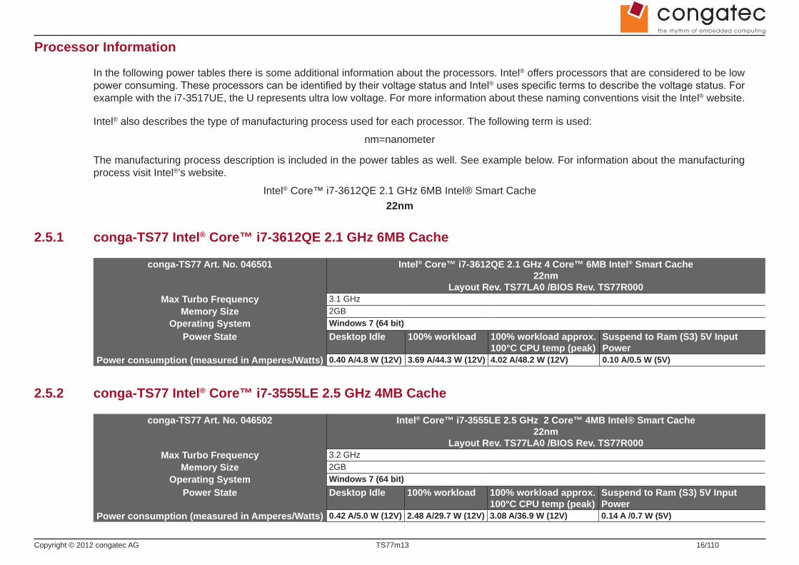
Processor Information
In the following power tables there is some additional information about the processors. Intel® offers processors that are considered to be low power consuming. These processors can be identified by their voltage status and Intel® uses specific terms to describe the voltage status. For example with the i7-3517UE, the U represents ultra low voltage. For more information about these naming conventions visit the Intel® website.
Intel® also describes the type of manufacturing process used for each processor. The following term is used:
nm=nanometer
The manufacturing process description is included in the power tables as well. See example below. For information about the manufacturing process visit Intel®’s website.
Intel® Core™ i7-3612QE 2.1 GHz 6MB Intel® Smart Cache22nm
2.5.1 conga-TS77 Intel® Core™ i7-3612QE 2.1 GHz 6MB Cache
conga-TS77 Art. No. 046501 Intel® Core™ i7-3612QE 2.1 GHz 4 Core™ 6MB Intel® Smart Cache22nm
Layout Rev. TS77LA0 /BIOS Rev. TS77R000Max Turbo Frequency 3.1 GHz
Memory Size 2GBOperating System Windows 7 (64 bit)
Power State Desktop Idle 100% workload 100% workload approx. 100°C CPU temp (peak)
Suspend to Ram (S3) 5V Input Power
Power consumption (measured in Amperes/Watts) 0.40 A/4.8 W (12V) 3.69 A/44.3 W (12V) 4.02 A/48.2 W (12V) 0.10 A/0.5 W (5V)
2.5.2 conga-TS77 Intel® Core™ i7-3555LE 2.5 GHz 4MB Cache
conga-TS77 Art. No. 046502 Intel® Core™ i7-3555LE 2.5 GHz 2 Core™ 4MB Intel® Smart Cache 22nm
Layout Rev. TS77LA0 /BIOS Rev. TS77R000Max Turbo Frequency 3.2 GHz
Memory Size 2GBOperating System Windows 7 (64 bit)
Power State Desktop Idle 100% workload 100% workload approx. 100°C CPU temp (peak)
Suspend to Ram (S3) 5V Input Power
Power consumption (measured in Amperes/Watts) 0.42 A/5.0 W (12V) 2.48 A/29.7 W (12V) 3.08 A/36.9 W (12V) 0.14 A /0.7 W (5V)

Copyright © 2012 congatec AG TS77m13 17/110
2.5.3 conga-TS77 Intel® Core™ i7-3517UE 1.7 GHz 4MB Cache
conga-TS77 Art. No. 046503 Intel® Core™ i7-3517UE 1.7 GHz 2 Core™ 4MB Intel® Smart Cache 22nm
Layout Rev. TS77LA0 /BIOS Rev. TS77R000Max Turbo Frequency 2.8 GHz
Memory Size 2GBOperating System Windows 7 (64 bit)
Power State Desktop Idle 100% workload 100% workload approx. 100°C CPU temp (peak)
Suspend to Ram (S3) 5V Input Power
Power consumption (measured in Amperes/Watts) 0.39 A/4.7 W (12V) 1.98 A/23.7 W (12V) 2.33 A/27.9 W (12V) 0.1 A/0.5 W (5V)
2.5.4 conga-TS77 Intel® Core™ i7-3615QE 2.3 GHz 6MB Cache
conga-TS77 Art. No. 046506 Intel® Core™ i7-3615QE 2.3 GHz 4 Core™ 6MB Intel® Smart Cache22nm
Layout Rev. TS77LA0 /BIOS Rev. TS77R000Max Turbo Frequency 3.3 GHz
Memory Size 2GBOperating System Windows 7 (64 bit)
Power State Desktop Idle 100% workload 100% workload approx. 100°C CPU temp (peak)
Suspend to Ram (S3) 5V Input Power
Power consumption (measured in Amperes/Watts) 0.42 A/5.0 W (12V) 4.85 A/58.2 W (12V) 4.48 A/53.7 W (12V) 0.14 A/0.7 W (5V)
2.5.5 conga-TS77 Intel® Core™ i5-3610ME 2.7 GHz 3MB Cache
conga-TS77 Art. No. 046504 Intel® Core™ i5-3610ME 2.7 GHz 2 Core™ 3MB Intel® Smart Cache22nm
Layout Rev. TS77LA0 /BIOS Rev. TS77R000Max Turbo Frequency 3.3 MHz
Memory Size 2GBOperating System Windows 7 (64 bit)
Power State Desktop Idle 100% workload 100% workload approx. 100°C CPU temp (peak)
Suspend to Ram (S3) 5V Input Power
Power consumption (measured in Amperes/Watts) 0.39 A/4.7 W (12V) 2.50 A/30.0 W (12V) 4.20 A/50.4 W (12V) 0.10 A/0.5 W (5V)

Copyright © 2012 congatec AG TS77m13 18/110
2.5.6 conga-TS77 Intel® Core™ i3-3217UE 1.6 GHz 3MB Cache
conga-TS77 Art. No. 046505 Intel® Core™ i3-3217UE 1.6 GHz 2 Core™ 3MB Intel® Smart Cache 22nm
Layout Rev. TS77LA0 /BIOS Rev. TS77R000Max Turbo Frequency Not supported
Memory Size 2GBOperating System Windows 7 (64 bit)
Power State Desktop Idle 100% workload 100% workload approx. 100°C CPU temp (peak)
Suspend to Ram (S3) 5V Input Power
Power consumption (measured in Amperes/Watts) 0.37 A/4.4 W (12V) 1.18 A/14.2 W (12V) 2.44 A/29.3 W (12V) 0.10 A/0.5 W (5V)
2.5.7 conga-TS77 Intel® Core™ i3-3120ME 2.4 GHz 3MB Cache
conga-TS77 Art. No. 046507 Intel® i3-3120ME 2.4 GHz 2 Core™ 3MB Intel® Smart Cache22nm
Layout Rev. TS77LA0 /BIOS Rev. TS77R000Max Turbo Frequency Not supported
Memory Size 2GBOperating System Windows 7 (64 bit)
Power State Desktop Idle 100% workload 100% workload approx. 100°C CPU temp (peak)
Suspend to Ram (S3) 5V Input Power
Power consumption (measured in Amperes/Watts) 0.40 A/4.8 W (12V) 1.69 A/20.3 W (12V) 3.26 A/39.1 W (12V) 0.10 A/0.5 W (5V)
2.5.8 conga-TS77 Intel® Celeron® 827E 1.4 GHz 1 Core™ 1.5MB Cache
conga-TS77 Art. No. 046508 Intel® Celeron® 827E 1.4 GHz 1 Core™ 1.5MB Intel® Smart Cache 32nm
Layout Rev. TS77LX0 /BIOS Rev. TS77R000Max Turbo Frequency Not supported
Memory Size 2GBOperating System Windows 7 (64 bit)
Power State Desktop Idle 100% workload 100% workload approx. 100°C CPU temp (peak)
Suspend to Ram (S3) 5V Input Power
Power consumption (measured in Amperes/Watts) 0.57 A/6.9 W (12V) 1.08 A/12.9 W (12V) 2.19 A/26.3 W (12V) 0.10 A/0.5 W (5V)

Copyright © 2012 congatec AG TS77m13 19/110
2.5.9 conga-TS77 Intel® Celeron® 847E 1.1 GHz 2 Core™ 2MB Cache
conga-TS77 Art. No. 046509 Intel® Celeron® 847E 1.1 GHz 2 Core™ 2MB Intel® Smart Cache 32nm
Layout Rev. TS77LX0 /BIOS Rev. TS77R000Max Turbo Frequency Not supported
Memory Size 2GBOperating System Windows 7 (64 bit)
Power State Desktop Idle 100% workload 100% workload approx. 100°C CPU temp (peak)
Suspend to Ram (S3) 5V Input Power
Power consumption (measured in Amperes/Watts) 0.57 A/6.9 W (12V) 1.30 A/15.6 W (12V) 1.39 A/16.7 W (12V) 0.10 A/0.5 W (5V)
2.5.10 conga-TS77 Intel® Celeron® 1047UE 1.4 GHz 2 Core™ 2MB Cache
conga-TS77 Art. No. 046510 Intel® Celeron® 1047UE 1.4 GHz 2 Core™ 2MB Intel® Smart Cache 22nm
Layout Rev. TS77LX0 /BIOS Rev. TS77R000Max Turbo Frequency Not supported
Memory Size 2GBOperating System Windows 7 (64 bit)
Power State Desktop Idle 100% workload 100% workload approx. 100°C CPU temp (peak)
Suspend to Ram (S3) 5V Input Power
Power consumption (measured in Amperes/Watts) 0.37 A/4.4 W (12V) 0.98 A/11.7 W (12V) 1.39 A/16.7 W (12V) 0.10 A/0.5 W (5V)
2.5.11 conga-TS77 Intel® Celeron® 1020E 2.2 GHz 2 Core™ 2MB Cache
conga-TS77 Art. No. 046511 Intel® Celeron® 1020E 2.2 GHz 2 Core™ 2MB Intel® Smart Cache 22nm
Layout Rev. TS77LX0 /BIOS Rev. TS77R000Max Turbo Frequency Not supported
Memory Size 2GBOperating System Windows 7 (64 bit)
Power State Desktop Idle 100% workload 100% workload approx. 100°C CPU temp (peak)
Suspend to Ram (S3) 5V Input Power
Power consumption (measured in Amperes/Watts) 0.37 A/4.4 W (12V) 1.54 A/18.5 W (12V) 2.23 A/26.8 W (12V) 0.08 A/0.4 W (5V)
Copyright © 2012 congatec AG TS77m13 20/110
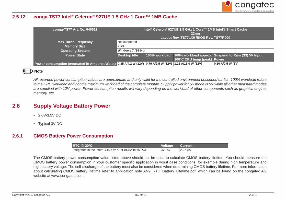
2.5.12 conga-TS77 Intel® Celeron® 927UE 1.5 GHz 1 Core™ 1MB Cache
conga-TS77 Art. No. 046512 Intel® Celeron® 927UE 1.5 GHz 1 Core™ 1MB Intel® Smart Cache 22nm
Layout Rev. TS77LX0 /BIOS Rev. TS77R000Max Turbo Frequency Not supported
Memory Size 2GBOperating System Windows 7 (64 bit)
Power State Desktop Idle 100% workload 100% workload approx. 100°C CPU temp (peak)
Suspend to Ram (S3) 5V Input Power
Power consumption (measured in Amperes/Watts) 0.35 A/4.2 W (12V) 0.79 A/9.5 W (12V) 1.25 A/15.0 W (12V) 0.10 A/0.5 W (5V)
Note
All recorded power consumption values are approximate and only valid for the controlled environment described earlier. 100% workload refers to the CPU workload and not the maximum workload of the complete module. Supply power for S3 mode is 5V while all other measured modes are supplied with 12V power. Power consumption results will vary depending on the workload of other components such as graphics engine, memory, etc.
2.6 Supply Voltage Battery Power• 2.0V-3.5V DC
• Typical 3V DC
2.6.1 CMOS Battery Power Consumption
RTC @ 20ºC Voltage CurrentIntegrated in the Intel® BD82QM77 or BD82HM76 PCH 3V DC 2.27 µA
The CMOS battery power consumption value listed above should not be used to calculate CMOS battery lifetime. You should measure the CMOS battery power consumption in your customer specific application in worst case conditions, for example during high temperature and high battery voltage. The self-discharge of the battery must also be considered when determining CMOS battery lifetime. For more information about calculating CMOS battery lifetime refer to application note AN9_RTC_Battery_Lifetime.pdf, which can be found on the congatec AG website at www.congatec.com.

Copyright © 2012 congatec AG TS77m13 21/110
2.7 Environmental SpecificationsTemperature Operation: 0° to 60°C Storage: -20° to +80°C
Humidity Operation: 10% to 90% Storage: 5% to 95%
Caution
The above operating temperatures must be strictly adhered to at all times. When using a heatspreader the maximum operating temperature refers to any measurable spot on the heatspreader’s surface.
congatec AG strongly recommends that you use the appropriate congatec module heatspreader as a thermal interface between the module and your application specific cooling solution.
If for some reason it is not possible to use the appropriate congatec module heatspreader, then it is the responsibility of the operator to ensure that all components found on the module operate within the component manufacturer’s specified temperature range.
For more information about operating a congatec module without heatspreader contact congatec technical support.
Humidity specifications are for non-condensing conditions.

Copyright © 2012 congatec AG TS77m13 22/110
3 Block Diagram
C-D
A-B
Intel®82579LM
GB Ethernet PHY
Hardware Monitoringand
Fan Control Circuitry
Mobile Intel® QM77Express Chipset
Intel® BD82QM77 PCH
RTCBoard Controller
STMicroelectronicsSTM32
Watchdog
BIOS(Flash)
DDR3-SODIMMSocket (top)
DDR3-SODIMMSocket (bottom)
CORE CORE
CORE CORE
GraphicsCORE
MemoryController
(Intel® BD82HM76 PCH forIntel® Celeron® equipped modules)
Processor
3rd GenerationIntel® Core™ i7Intel® Core™ i5Intel® Core™ i3 Intel® Celeron®
2nd Generation Intel® Celeron®
8x U
SB 2.
0
LCD
I/F (LV
DS)
VGA
High
Defi
nition
Aud
io (H
DA) I/
F
4xSA
TA
GPIOs
SPII2C
Fan C
ontro
l
Powe
r Man
agem
ent a
nd C
ontro
l Sign
als
Gbit E
ther
net
SM B
us
4x U
SB 3.
0 Sign
als
x1 P
CIe L
ink
6 PCI
e Lan
es1 P
CIe L
ane
DMI x4(Direct Media
Interface)
Intel® FDI(Flexible Display
Interface) 8 PCIe Lanes
16 GByte Max. Total 1 PE
G x
16
SDVO
/ H
DM
I / D
P
HD
MI /
DP
HD
MI /
DP
GPI
s/G
POs
Memory Types(1066 or 1333 or 1600 MT/s)
TPM(optional)
LPC
Bus

Copyright © 2012 congatec AG TS77m13 23/110
4 HeatspreaderAn important factor for each system integration is the thermal design. The heatspreader acts as a thermal coupling device to the module and its aluminum plate is 3mm thick.
The heatspreader is thermally coupled to the CPU and other heat generating components via a heat pipe.
Although the heatspreader is the thermal interface where most of the heat generated by the module is dissipated, it is not to be considered as a heatsink. It has been designed as a thermal interface between the module and the application specific thermal solution. The application specific thermal solution may use heatsinks with fans, and/or heat pipes, which can be attached to the heatspreader. Some thermal solutions may also require that the heatspreader is attached directly to the systems chassis thereby using the whole chassis as a heat dissipater.
For additional information about the conga-TS77 heatspreader, refer to section 4.2 of this document.
Caution
There are mounting holes on the heatspreader designed to attach the heatspreader to the module. These mounting holes must be used to ensure that all components that are required to make contact with heatspreader do so. Failure to utilize these mounting holes will result in improper contact between these components and heatspreader thereby reducing heat dissipation efficiency.
Attention must be given to the mounting solution used to mount the heatspreader and module into the system chassis. Do not use a threaded heatspreader together with threaded carrier board standoffs. The combination of the two threads may be staggered, which could lead to stripping or cross-threading of the threads in either the standoffs of the heatspreader or carrier board.
Copyright © 2012 congatec AG TS77m13 24/110
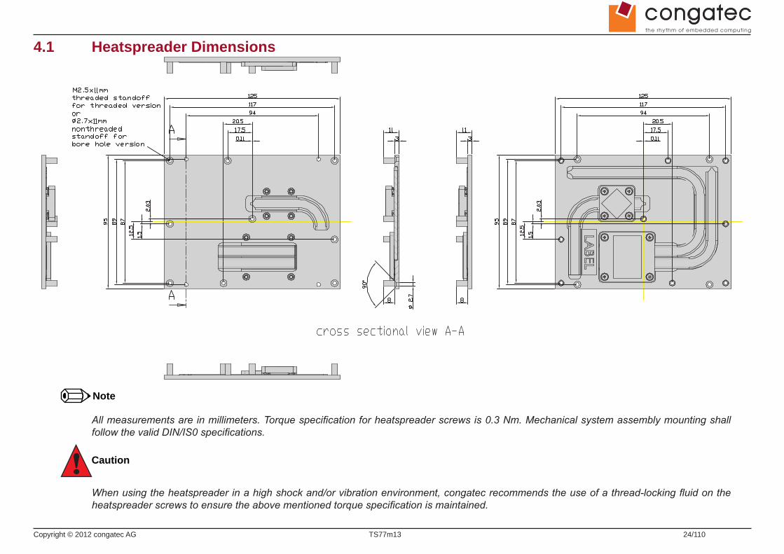
4.1 Heatspreader Dimensions
Note
All measurements are in millimeters. Torque specification for heatspreader screws is 0.3 Nm. Mechanical system assembly mounting shall follow the valid DIN/IS0 specifications.
Caution
When using the heatspreader in a high shock and/or vibration environment, congatec recommends the use of a thread-locking fluid on the heatspreader screws to ensure the above mentioned torque specification is maintained.

Copyright © 2012 congatec AG TS77m13 25/110
4.2 Heatspreader Thermal ImageryThe conga-TS77 heatspreader solution features heat pipes. A heat pipe is a simple device that can quickly transfer heat from one point to another. They are often referred to as the “superconductors” of heat as they possess an extra ordinary heat transfer capacity and rate with almost no heat loss. The thermal image below provides a reference to where the heat is being transferred to on the heatspreader surface area when using the conga-BM57, which is similar to conga-TS77. All surface temperatures shown in the thermal image are in centigrade. System designers must ensure that the system’s cooling solution is designed to dissipate the heat from the hottest surface spots of the heatspreader.

Copyright © 2012 congatec AG TS77m13 26/110
5 Onboard Temperature SensorsOnboard the conga-TS77 are two sensors - the board temperature sensor and the system environment temperature sensor. These sensors are defined in the CGOS API as CGOS_TEMP_BOARD and CGOS_TEMP_ENV.
Board Temperature Sensor:
The board sensor is located at the top of the conga-TS77. This sensor measures the board temperature and is defined in CGOS API as CGOS_TEMP_BOARD. It is located on the module as shown below:
Sensor Location

Copyright © 2012 congatec AG TS77m13 27/110
System Environment Temperature Sensor:
The system environment sensor is located at the bottom of the conga-TS77. This sensor measures the system environment temperature and is defined in CGOS API as CGOS_TEMP_ENV. It is located on the module as shown below:
sensor location
Copyright © 2012 congatec AG TS77m13 28/110
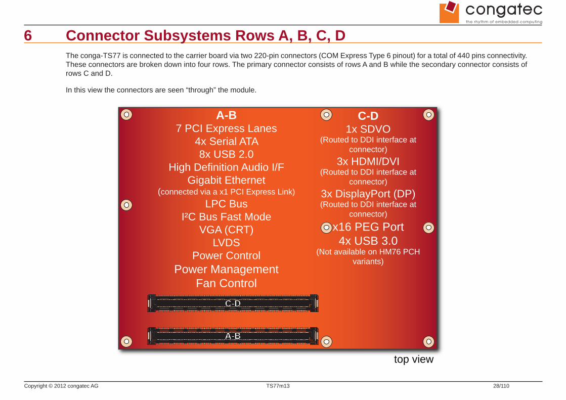
6 Connector Subsystems Rows A, B, C, DThe conga-TS77 is connected to the carrier board via two 220-pin connectors (COM Express Type 6 pinout) for a total of 440 pins connectivity. These connectors are broken down into four rows. The primary connector consists of rows A and B while the secondary connector consists of rows C and D.
In this view the connectors are seen “through” the module.
top view
A-B7 PCI Express Lanes
4x Serial ATA8x USB 2.0
High Definition Audio I/FGigabit Ethernet
(connected via a x1 PCI Express Link)LPC Bus
I²C Bus Fast ModeVGA (CRT)
LVDSPower Control
Power ManagementFan Control
C-D1x SDVO
(Routed to DDI interface atconnector)
3x HDMI/DVI(Routed to DDI interface at
connector)3x DisplayPort (DP)(Routed to DDI interface at
connector)
x16 PEG Port4x USB 3.0
(Not available on HM76 PCHvariants)
C-D
A-B

Copyright © 2012 congatec AG TS77m13 29/110
6.1 Primary Connector Rows A and BThe following subsystems can be found on the primary connector rows A and B.
6.1.1 Serial ATA™ (SATA)
Six Serial ATA connections are provided via the Intel® BD82QM77 or BD82HM76 (QM77 or HM76) PCH. The conga-TS77 provides 4 SATA ports (SATA 0-3) externally. Two of these SATA ports (SATA 0 and 1) support Gen 3 with up to 6.0 Gb/s transfer rate. The other two SATA ports (SATA 2 and 3) are Gen 2.6 compliant, supporting transfer rates up to 3Gb/s.
6.1.2 USB 2.0
The conga-TS77 offers two EHCI USB host controllers that support USB high speed signalling via Intel® BD82QM77 or BD82HM76 (QM77 or HM76) PCH. These controllers comply with USB standard 1.1 and 2.0 and offer a total of 8 USB ports via connector rows A and B. Each port is capable of supporting USB 1.1 and 2.0 compliant devices. For more information about how the USB host controllers are routed see section 8.6.
6.1.3 High Definition Audio (HDA) Interface
The conga-TS77 provides an interface that supports the connection of HDA audio codecs.
6.1.4 Gigabit Ethernet
The conga-TS77 is equipped with a Gigabit Ethernet Controller that is integrated within the Intel® BD82QM77 or BD82HM76 (QM77 or HM76) PCH. This controller is combined with an Intel® 82579LM Phy that is implemented through the use of the seventh PCI Express lane. The Ethernet interface consists of 4 pairs of low voltage differential pair signals designated from GBE0_MD0± to GBE0_MD3± plus control signals for link activity indicators. These signals can be used to connect to a 10/100/1000 BaseT RJ45 connector with integrated or external isolation magnetics on the carrier board.
Note
The GBE0_LINK# output is only active during a 100Mbit or 1Gbit connection, it is not active during a 10Mbit connection. This is a limitation of Ethernet controller since it only has 3 LED outputs, ACT#, LINK100# and LINK1000#. The GBE0_LINK# signal is a logic AND of the GBE0_LINK100# and GBE0_LINK1000# signals on the conga-TS77 module.

Copyright © 2012 congatec AG TS77m13 30/110
6.1.5 LPC Bus
conga-TS77 offers the LPC (Low Pin Count) bus through the use of the Intel® BD82QM77 or BD82HM76 (QM77 or HM76) PCH. There are many devices available for this Intel® defined bus. The LPC bus corresponds approximately to a serialized ISA bus yet with a significantly reduced number of signals. Due to the software compatibility to the ISA bus, I/O extensions such as additional serial ports can be easily implemented on an application specific baseboard using this bus. See section 10.2.1 for more information about the LPC Bus.
6.1.6 I²C Bus Fast Mode
The I²C bus is implemented through the congatec board controller (STMicroelectronics STM32) and accessed through the congatec CGOS driver and API. The controller provides a Fast Mode multi-master I²C Bus that has maximum I²C bandwidth.
6.1.7 PCI Express™
The conga-TS77 offers 8 PCI Express™ lanes via the Intel® BD82QM77 or BD82HM76 (QM77 or HM76) PCH. The Gen 2 PCI Express™ interface offers support for full 5 Gb/s bandwidth in each direction per x1 link.
One of the eight PCI Express lanes is utilized by the onboard Gigabit Ethernet interface. Six PCI Express lanes are available on the A,B connector row. Default configuration for these 6 lanes is 6x1 link. A 1x4 and 2x1 link configuration is also possible but requires a special/customized BIOS firmware. Contact congatec technical support for more information about this subject.
The PCI Express interface is based on the PCI Express Specification 2.0 with Gen 1 (2.5Gb/s) and Gen 2 (5 Gb/s) speed.
6.1.8 ExpressCard™
The conga-TS77 supports the implementation of ExpressCards, which requires the dedication of one USB port or a x1 PCI Express link for each ExpressCard used.
6.1.9 Graphics Output (VGA/CRT)
The conga-TS77 graphics are driven by a Mobile Intel® 7 Series HD 4000 graphics engine, incorporated within the processor found on the conga-TS77. This graphic engine offers significantly higher performance than previous Intel® graphics engines found on previous Intel® chipsets.
Note
conga-TS77 variants that feature the Intel® HM76 PCH are driven by Mobile Intel® 6 Series HD graphics engine.

Copyright © 2012 congatec AG TS77m13 31/110
6.1.10 LCD
The Intel® BD82QM77 or BD82HM76 (QM77 or HM76) PCH, found on the conga-TS77, offers an integrated dual channel LVDS interface. There are two LVDS transmitter channels (Channel A and Channel B) in the LVDS interface. Channel A and Channel B consist of 4-data pairs and a clock pair each.
6.1.11 General Purpose Serial Interface
Two TTL compatible two wire ports are available on Type 6 COM Express modules. These pins are designated SER0_TX, SER0_RX, SER1_TX and SER1_RX. Data out of the module is on the _TX pins. Hardware handshaking and hardware flow control are not supported. The module asynchronous serial ports are intended for general purpose use and for use with debugging software that make use of the “console redirect” features available in many operating systems.
Note
The General Purpose Serial Interface is not supported on the conga-TS77 module.
6.1.12 Power Control
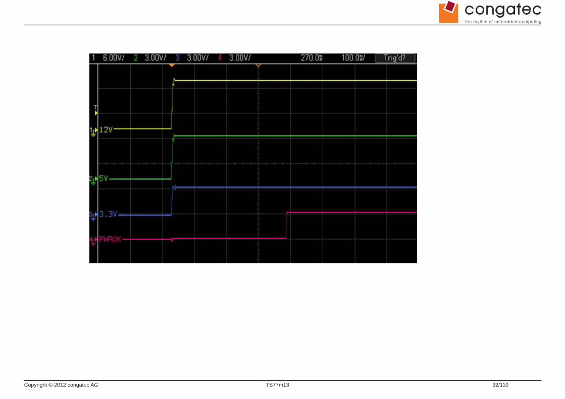
PWR_OK
Power OK from main power supply or carrier board voltage regulator circuitry. A high value indicates that the power is good and the module can start its onboard power sequencing.
Carrier board hardware must drive this signal low until all power rails and clocks are stable. Releasing PWR_OK too early or not driving it low at all can cause numerous boot up problems. It is a good design practice to delay the PWR_OK signal a little (typically 100ms) after all carrier board power rails are up, to ensure a stable system.
Note
The module is kept in reset as long as the PWR_OK is driven by carrier board hardware.
A sample screenshot is shown below:
Copyright © 2012 congatec AG TS77m13 32/110

Copyright © 2012 congatec AG TS77m13 33/110
The conga-TS77 PWR_OK input circuitry is implemented as shown below:
The voltage divider ensures that the input complies with 3.3V CMOS characteristic and also allows for carrier board designs that are not driving PWR_OK. Although the PWR_OK input is not mandatory for the onboard power-up sequencing, it is strongly recommended that the carrier board hardware drives the signal low until it is safe to let the module boot-up.
When considering the above shown voltage divider circuitry and the transistor stage, the voltage measured at the PWR_OK input pin may be only around 0.8V when the 12V is applied to the module. Actively driving PWR_OK high is compliant to the COM Express specification but this can cause back driving. Therefore, congatec recommends driving the PWR_OK low to keep the module in reset and tri-state PWR_OK when the carrier board hardware is ready to boot.
The three typical usage scenarios for a carrier board design are:
• Connect PWR_OK to the “power good” signal of an ATX type power supply.
• Connect PWR_OK to the last voltage regulator in the chain on the carrier board.
• Simply pull PWR_OK with a 1k resistor to the carrier board 3.3V power rail.
With this solution, it must be ensured that by the time the 3.3V is up, all carrier board hardware is fully powered and all clocks are stable.
To Module Power LogicPWR_OK
R5R1%47k5S02TB
TBC847
R4R1%100kS02
+V12.0_S0
R13R1%1k00S02
R1R1%47k5S02
R2R1%20k0S02
Copyright © 2012 congatec AG TS77m13 34/110
The conga-TS77 provides support for controlling ATX-style power supplies. When not using an ATX power supply then the conga-TS77’s pins SUS_S3/PS_ON, 5V_SB, and PWRBTN# should be left unconnected.
SUS_S3#/PS_ON#
The SUS_S3#/PS_ON# (pin A15 on the A-B connector) signal is an active-low output that can be used to turn on the main outputs of an ATX-style power supply. In order to accomplish this the signal must be inverted with an inverter/transistor that is supplied by standby voltage and is located on the carrier board.
PWRBTN#
When using ATX-style power supplies PWRBTN# (pin B12 on the A-B connector) is used to connect to a momentary-contact, active-low debounced push-button input while the other terminal on the push-button must be connected to ground. This signal is internally pulled up to 3V_SB using a 10k resistor. When PWRBTN# is asserted it indicates that an operator wants to turn the power on or off. The response to this signal from the system may vary as a result of modifications made in BIOS settings or by system software.
Power Supply Implementation Guidelines
12 volt input power is the sole operational power source for the conga-TS77. The remaining necessary voltages are internally generated on the module using onboard voltage regulators. A carrier board designer should be aware of the following important information when designing a power supply for a conga-TS77 application:
• It has also been noticed that on some occasions, problems occur when using a 12V power supply that produces non monotonic voltage when powered up. The problem is that some internal circuits on the module (e.g. clock-generator chips) will generate their own reset signals when the supply voltage exceeds a certain voltage threshold. A voltage dip after passing this threshold may lead to these circuits becoming confused resulting in a malfunction. It must be mentioned that this problem is quite rare but has been observed in some mobile power supply applications. The best way to ensure that this problem is not encountered is to observe the power supply rise waveform through the use of an oscilloscope to determine if the rise is indeed monotonic and does not have any dips. This should be done during the power supply qualification phase therefore ensuring that the above mentioned problem doesn’t arise in the application. For more information about this issue visit www.formfactors.org and view page 25 figure 7 of the document “ATX12V Power Supply Design Guide V2.2”.
6.1.13 Power Management
ACPI 3.0 compliant with battery support. Also supports Suspend to RAM (S3).

Copyright © 2012 congatec AG TS77m13 35/110
6.2 Secondary Connector Rows C and DThe following subsystems can be found on the secondary connector rows C and D.
6.2.1 PCI Express™
The conga-TS77 offers 8 PCI Express™ lanes via the Intel® BD82QM77 or BD82HM76 (QM77 or HM76) PCH. The Gen 2 PCI Express™ interface offers support for full 5 Gb/s bandwidth in each direction per x1 link. One of these PCI Express lanes (PCIe lane 7) is available on the C,D connector row.
The PCI Express interface is based on the PCI Express Specification 2.0 with Gen 1 (2.5Gb/s) and Gen 2 (5 Gb/s) speed.
6.2.2 PCI Express Graphics (PEG)
PCI Express Graphics (PEG) is supported on conga-TS77 variants. The PEG lanes are same as PCI Express lanes 16-31 and are fully compliant to the PCI Express Specification 3.0, with support for 8.0 Gb/s speed.
The x16 PEG interface is by default configured as a 1 x16 link. It is however possible to optionally configure the x16 PEG interface to support graphics and/or non-graphic PCI Express devices. This configuration increases the available PCI Express lanes on top of those explained in section 6.1.7 and section 6.2.1. It also enables the use of the PEG lanes for supporting x1, x2, x4 or x8 PCI Express devices.
PEGLANE0
Single Link (1x16 Link)
Link 1
Link 1
Link 1 Link 2 Link 3
Link 2
Double Links (2x8 Links)
Triple Links (1x8 + 2x4 Links)
PEGLANE1
PEGLANE2
PEGLANE3
PEGLANE4
PEGLANE5
PEGLANE6
PEGLANE7
PEGLANE8
PEGLANE9
PEGLANE10
PEGLANE11
PEGLANE12
PEGLANE13
PEGLANE14
PEGLANE15

Copyright © 2012 congatec AG TS77m13 36/110
The possible configurations as shown above are:
• 1 x16 link (default PEG)
• 2 x8 links
• 1 x8 + 2 x4 links
The sixteen PCIe lanes of the PEG interface are controlled by three controllers. Each controller can automatically operate on a lower link width allowing up to three simultaneous operating devices on the PEG interface. The PEG root port configuration can be selected in the BIOS setup program. This feature is only available on conga-TS77 variants with hardware revision A.x or later.
Note
The PEG lanes can not be linked together with the PCI Express lanes discussed in sections 6.1.7 and 6.2.1.
conga-TS77 variants that feature the Intel® HM76 PCH and Intel® i3 processors are PCI Express 2.0 compliant only. The variants that feature the Intel®Celeron 927UE processor do not support PEG.
6.2.3 SDVO
The Serial Digital Video Output (SDVO) is multiplexed with HDMI and DisplayPort on the Digital Display Interface channel 1 (DDI1) of the COM Express connector. It may be used for a third party SDVO compliant device connected to DDI1. See section 9.5 of this document for more information about enabling SDVO peripherals.
Note
The SDVO interface only supports the connection of DVI transmitters. The connection of other transmitters such as TV or LVDS is not supported.
The conga-TS77 provides three DDI’s that support three independent displays. To enable three independent displays, the combination must be 2 DisplayPort plus any other display
6.2.4 HDMI
The Intel® BD82QM77 or BD82HM76 (QM77 or HM76) PCH on the conga-TS77 supports integrated HDMI, which is multiplexed onto the Digital Display Interface (DDI) of the COM Express connector. The Intel® QM77 or HM76 provides three ports capable of supporting HDMI. See section 9.5 of this document for more information about enabling HDMI peripherals.
Note
Copyright © 2012 congatec AG TS77m13 37/110
The conga-TS77 provides three DDI’s that support three independent displays. To enable three independent displays, the combination must be 2 DisplayPort plus any other display.
6.2.5 DisplayPort (DP)
The conga-TS77 offers three DP ports, each capable of supporting link-speeds of 1.62 Gbps and 2.7 Gbps on 1, 2 or 4 data lanes. The DP is multiplexed onto the Digital Display Interface (DDI) of the COM Express connector. The DisplayPort specification is a VESA standard aimed at consolidating internal and external connection methods to reduce device complexity, supporting key cross industry applications, and providing performance scalability to enable the next generation of displays.
The Intel® BD82QM77 or BD82HM76 (QM77 or HM76) PCH supports a maximum of 3 DP ports simultaneously. See section 9.5 of this document for more information about enabling DisplayPort peripherals.
Note
The conga-TS77 provides three DDI’s that support three independent displays. To enable three independent displays, the combination must be 2 DisplayPort plus any other display.
6.2.6 USB 3.0
The conga-TS77 offers one xHCI host controller provided by the Intel® BD82QM77 (QM77) PCH. This controller supports up to four SuperSpeed USB 3.0 ports and allows data transfers up to 5 Gb/s. It also supports SuperSpeed, high-speed, full-speed and low-speed traffic on the bus.

Copyright © 2012 congatec AG TS77m13 38/110
7 Additional Features
7.1 congatec Board Controller (cBC)The conga-TS77 is equipped with a STMicroelectronics STM32 microcontroller. This onboard microcontroller plays an important role for most of the congatec embedded/industrial PC features. It fully isolates some of the embedded features such as system monitoring or the I²C bus from the x86 core architecture, which results in higher embedded feature performance and more reliability, even when the x86 processor is in a low power mode. It also ensures that the congatec embedded feature set is fully compatible amongst all congatec modules.
7.2 Board InformationThe cBC provides a rich data-set of manufacturing and board information such as serial number, EAN number, hardware and firmware revisions, and so on. It also keeps track of dynamically changing data like runtime meter and boot counter.
7.3 WatchdogThe conga-TS77 is equipped with a multi stage watchdog solution that is triggered by software. The COM Express™ Specification does not provide support for external hardware triggering of the Watchdog, which means the conga-TS77 does not support external hardware triggering. For more information about the Watchdog feature, see the BIOS setup description in section 11.4.2 of this document and application note AN3_Watchdog.pdf on the congatec AG website at www.congatec.com.
Note
The conga-TS77 module does not support the watchdog NMI mode. COM Express type 6 modules do not support the PCI bus and therefore the PCI_SERR# signal is not available. There is no way to drive a NMI to the processor without the presence of the PCI_SERR# PCI bus signal.
7.4 I2C BusThe conga-TS77 offers support for the frequently used I2C bus. Thanks to the I2C host controller in the cBC, the I2C bus is multimaster capable and runs at fast mode.

Copyright © 2012 congatec AG TS77m13 39/110
7.5 Power Loss ControlThe cBC has full control of the power-up of the module and therefore can be used to specify the behaviour of the system after a AC power loss condition. Supported modes are “Always On”, “Remain Off” and “Last State”.
7.6 Embedded BIOSThe conga-TS77 is equipped with congatec Embedded BIOS, which is based on American Megatrends Inc. Aptio UEFI firmware. These are the most important embedded PC features:
7.6.1 CMOS Backup in Non Volatile Memory
A copy of the CMOS memory (SRAM) is stored in the BIOS flash device. This prevents the system from not booting up with the correct system configuration if the backup battery (RTC battery) has failed. Additionally, it provides the ability to create systems that do not require a CMOS backup battery.
7.6.2 OEM CMOS Default Settings and OEM BIOS Logo
This feature allows system designers to create and store their own CMOS default configuration and BIOS logo (splash screen) within the BIOS flash device. Customized BIOS development by congatec for these changes is no longer necessary because customers can easily do these changes by themselves using the congatec system utility CGUITL.
7.6.3 OEM BIOS Code
With the congatec embedded BIOS it is even possible for system designers to add their own code to the BIOS POST process. Except for custom specific code, this feature can also be used to support Win XP SLP installation, Window 7 SLIC table, verb tables for HDA codecs, rare graphic modes and Super I/O controllers.
For more information about customizing the congatec embedded BIOS refer to the congatec System Utility user’s guide, which is called CGUTLm1x.pdf and can be found on the congatec AG website at www.congatec.com or contact congatec technical support.
Copyright © 2012 congatec AG TS77m13 40/110
7.6.4 congatec Battery Management Interface
In order to facilitate the development of battery powered mobile systems based on embedded modules, congatec AG has defined an interface for the exchange of data between a CPU module (using an ACPI operating system) and a Smart Battery system. A system developed according to the congatec Battery Management Interface Specification can provide the battery management functions supported by an ACPI capable operating system (e.g. charge state of the battery, information about the battery, alarms/events for certain battery states, ...) without the need for any additional modifications to the system BIOS.
The conga-TS77 BIOS fully supports this interface. For more information about this subject visit the congatec website and view the following documents:
• congatec Battery Management Interface Specification
• Battery System Design Guide
• conga-SBM3 User’s Guide
7.6.5 API Support (CGOS/EAPI)
In order to benefit from the above mentioned non-industry standard feature set, congatec provides an API that allows application software developers to easily integrate all these features into their code. The CGOS API (congatec Operating System Application Programming Interface) is the congatec proprietary API that is available for all commonly used Operating Systems such as Win32, Win64, Win CE, Linux. The architecture of the CGOS API driver provides the ability to write application software that runs unmodified on all congatec CPU modules. All the hardware related code is contained within the congatec embedded BIOS on the module. See section 1.1 of the CGOS API software developers guide, which is available on the congatec website .
Other COM (Computer on Modules) vendors offer similar driver solutions for these kind of embedded PC features, which are by nature proprietary. All the API solutions that can be found on the market are not compatible to each other. As a result, writing application software that can run on more than one vendor’s COM is not so easy. Customers have to change their application software when switching to another COM vendor. EAPI (Embedded Application Programming Interface) is a programming interface defined by the PICMG that addresses this problem. With this unified API it is now possible to run the same application on all vendor’s COMs that offer EAPI driver support. Contact congatec technical support for more information about EAPI.

Copyright © 2012 congatec AG TS77m13 41/110
7.7 Security FeaturesThe conga-TS77 can be equipped optionally with a “Trusted Platform Module“ (TPM 1.2). This TPM 1.2 includes coprocessors to calculate efficient hash and RSA algorithms with key lengths up to 2,048 bits as well as a real random number generator. Security sensitive applications like gaming and e-commerce will benefit also with improved authentication, integrity and confidence levels.
7.8 Suspend to RamThe Suspend to RAM feature is available on the conga-TS77.
Copyright © 2012 congatec AG TS77m13 42/110
8 conga Tech NotesThe conga-TS77 has some technological features that require additional explanation. The following section will give the reader a better understanding of some of these features. This information will also help to gain a better understanding of the information found in the System Resources section of this user’s guide as well as some of the setup nodes found in the BIOS Setup Program description section.
8.1 Intel Turbo Boost 2Intel® Turbo Boost 2 Technology allows processor cores to run faster than the base operating frequency if it’s operating below power, current, and temperature specification limits. Intel® Turbo Boost 2 Technology is activated when the Operating System (OS) requests the highest processor performance state. The maximum frequency of Intel® Turbo Boost 2 Technology is dependent on the number of active cores. The amount of time the processor spends in the Intel Turbo Boost 2 Technology state depends on the workload and operating environment. Any of the following can set the upper limit of Intel® Turbo Boost 2 Technology on a given workload:
• Number of active cores
• Estimated current consumption
• Estimated power consumption
• Processor temperature
When the processor is operating below these limits and the user’s workload demands additional performance, the processor frequency will dynamically increase by 100 MHz on short and regular intervals until the upper limit is met or the maximum possible upside for the number of active cores is reached. For more information about Intel® Turbo Boost 2 Technology visit the Intel® website.
Note
Only conga-TS77 module variants that feature the Core™ i7 and i5 processors support Intel® Turbo Boost 2 Technology. Refer to the power consumption tables in section 2.5 of this document for information about the max turbo frequency available for each variant of the conga-TS77.

Copyright © 2012 congatec AG TS77m13 43/110
8.2 Intel® Matrix Storage Technology The Intel® BD82QM77 or BD82HM76 (QM77 or HM76) PCH provides support for Intel® Matrix Storage Technology, allowing AHCI functionality, RAID 0/1/5/10 Support and Intel® Smart Response Technology.
8.2.1 AHCI
The QM77 or HM76 provides hardware support for Advanced Host Controller Interface (AHCI), a new programming interface for SATA host controllers. Platforms supporting AHCI may take advantage of performance features such as no master/slave designation for SATA devices (each device is treated as a master) and hardware-assisted native command queuing. AHCI also provides usability enhancements such as Hot-Plug.
8.2.2 RAID
The industry-leading RAID capability provides high performance RAID 0, 1, 5, and 10 functionality on the 4 SATA ports of Intel® BD82QM77 (QM77) PCH. Software components include an Option ROM for pre-boot configuration and boot functionality, a Microsoft* Windows* compatible driver, and a user interface for configuration and management of the RAID capability of the Intel® BD82QM77 (QM77) PCH.
Note
RAID support is not available on conga-TS77 variants that feature the Intel® BD82HM76 (HM76) chipset.
8.2.3 Intel® Smart Response Technology
Intel® Smart Response Technology is a disk caching solution that can provide improved computer system performance with improved power savings. It allows configuration of a computer systems with the advantage of having HDDs for maximum storage capacity with system performance at or near SSD performance levels.

Copyright © 2012 congatec AG TS77m13 44/110
8.3 Intel® Processor Features
8.3.1 Thermal Monitor and Catastrophic Thermal Protection
Intel® Core™ i7/i5/i3 and Celeron® processors have a thermal monitor feature that helps to control the processor temperature. The integrated TCC (Thermal Control Circuit) activates if the processor silicon reaches its maximum operating temperature. The activation temperature, that the Intel® Thermal Monitor uses to activate the TCC, cannot be configured by the user nor is it software visible.
The Thermal Monitor can control the processor temperature through the use of two different methods defined as TM1 and TM2. TM1 method consists of the modulation (starting and stopping) of the processor clocks at a 50% duty cycle. The TM2 method initiates an Enhanced Intel Speedstep transition to the lowest performance state once the processor silicon reaches the maximum operating temperature.
Note
The maximum operating temperature for Intel® Core™ i7/i5/i3 and Celeron® processors is 100°C. TM2 mode is used for Intel® Core™ i7/i5/i3 and the latest generation of Celeron® processors.
Two modes are supported by the Thermal Monitor to activate the TCC. They are called Automatic and On-Demand. No additional hardware, software, or handling routines are necessary when using Automatic Mode.
Note
To ensure that the TCC is active for only short periods of time, thus reducing the impact on processor performance to a minimum, it is necessary to have a properly designed thermal solution. The Intel® Core™ i7/i5/i3 and Celeron® processor’s respective datasheet can provide you with more information about this subject.
THERMTRIP# signal is used by Intel®’s Core™ i7/i5/i3 and Celeron® processors for catastrophic thermal protection. If the processor’s silicon reaches a temperature of approximately 125°C then the processor signal THERMTRIP# will go active and the system will automatically shut down to prevent any damage to the processor as a result of overheating. The THERMTRIP# signal activation is completely independent from processor activity and therefore does not produce any bus cycles.
Note
In order for THERMTRIP# to be able to automatically switch off the system, it is necessary to use an ATX style power supply.
Copyright © 2012 congatec AG TS77m13 45/110
8.3.2 Processor Performance Control
Intel® Core™ i7/i5/i3 and Celeron® processors found on the conga-TS77 run at different voltage/frequency states (performance states), which is referred to as Enhanced Intel® SpeedStep® technology (EIST). Operating systems that support performance control take advantage of microprocessors that use several different performance states in order to efficiently operate the processor when it’s not being fully utilized. The operating system will determine the necessary performance state that the processor should run at so that the optimal balance between performance and power consumption can be achieved during runtime.
The Windows family of operating systems links its processor performance control policy to the power scheme setting. You must ensure that your power scheme setting you choose, has the ability to support Enhanced Intel® SpeedStep® technology.
8.3.3 Intel® 64
The formerly known Intel® Extended Memory 64 Technology is an enhancement to Intel®’s IA-32 architecture. Intel® 64 is only available on Intel® Core™ i7/i5/i3 and Celeron® processors and is designed to run with newly written 64-bit code and access more than 4GB of memory. Processors with Intel® 64 architecture support 64-bit-capable operating systems from Microsoft, Red Hat and SuSE. Processors running in legacy mode remain fully compatible with today’s existing 32-bit applications and operating systems
Platforms with Intel® 64 can be run in three basic ways :
1. Legacy Mode: 32-bit operating system and 32-bit applications. In this mode no software changes are required, however the benefits of Intel® 64 are not utilized.
2. Compatibility Mode: 64-bit operating system and 32-bit applications. This mode requires all device drivers to be 64-bit. The operating system will see the 64-bit extensions but the 32-bit application will not. Existing 32-bit applications do not need to be recompiled and may or may not benefit from the 64-bit extensions. The application will likely need to be re-certified by the vendor to run on the new 64-bit extended operating system.
3. 64-bit Mode: 64-bit operating system and 64-bit applications. This usage requires 64-bit device drivers. It also requires applications to be modified for 64-bit operation and then recompiled and validated.
Intel® 64 provides support for:
• 64-bit flat virtual address space
• 64-bit pointers
• 64-bit wide general purpose registers
Copyright © 2012 congatec AG TS77m13 46/110
• 64-bit integer support
• Up to one Terabyte (TB) of platform address space
You can find more information about Intel® 64 Technology at: http://developer.intel.com/technology/intel64/index.htm
8.3.4 Intel® Virtualization Technology
Virtualization solutions enhanced by Intel® VT will allow a Core™ i7/i5/i3 platform to run multiple operating systems and applications in independent partitions. When using virtualization capabilities, one computer system can function as multiple “virtual” systems. With processor and I/O enhancements to Intel®’s various platforms, Intel® Virtualization Technology can improve the performance and robustness of today’s software-only virtual machine solutions.
Intel® VT is a multi-generational series of extensions to Intel® processor and platform architecture that provides a new hardware foundation for virtualization, establishing a common infrastructure for all classes of Intel® based systems. The broad availability of Intel® VT makes it possible to create entirely new applications for virtualization in servers, clients as well as embedded systems thus providing new ways to improve system reliability, manageability, security, and real-time quality of service.
The success of any new hardware architecture is highly dependent on the system software that puts its new features to use. In the case of virtualization technology, that support comes from the virtual machine monitor (VMM), a layer of software that controls the underlying physical platform resources sharing them between multiple “guest” operating systems. Intel® VT is already incorporated into most commercial and open-source VMMs including those from VMware, Microsoft, XenSource, Parallels, Virtual Iron, Jaluna and TenAsys.
You can find more information about Intel Virtualization Technology at: http://developer.intel.com/technology/virtualization/index.htm
Note
congatec does not offer virtual machine monitor (VMM) software. All VMM software support questions and queries should be directed to the VMM software vendor and not congatec technical support.
8.4 Thermal ManagementACPI is responsible for allowing the operating system to play an important part in the system’s thermal management. This results in the operating system having the ability to take control of the operating environment by implementing cooling decisions according to the demands put on the CPU by the application.

Copyright © 2012 congatec AG TS77m13 47/110
The conga-TS77 ACPI thermal solution offers three different cooling policies:
• Passive Cooling
When the temperature in the thermal zone must be reduced, the operating system can decrease the power consumption of the processor by throttling the processor clock. One of the advantages of this cooling policy is that passive cooling devices (in this case the processor) do not produce any noise. Use the “passive cooling trip point” setup node in the BIOS setup program to determine the temperature threshold that the operating system will use to start or stop the passive cooling procedure.
• Active Cooling
During this cooling policy the operating system is turning the fan on/off. Although active cooling devices consume power and produce noise, they also have the ability to cool the thermal zone without having to reduce the overall system performance. Use the “active cooling trip point” setup node in the BIOS setup program to determine the temperature threshold that the operating system will use to start the active cooling device. It is stopped again when the temperature goes below the threshold (4°C hysteresis).
• Critical Trip Point
If the temperature in the thermal zone reaches a critical point then the operating system will perform a system shut down in an orderly fashion in order to ensure that there is no damage done to the system as result of high temperatures. Use the “critical trip point” setup node in the BIOS setup program to determine the temperature threshold that the operating system will use to shut down the system.
Note
The end user must determine the cooling preferences for the system by using the setup nodes in the BIOS setup program to establish the appropriate trip points. If passive cooling is activated and the processor temperature is above the trip point the processor clock is throttled according to the formula below.
∆P[%] = TC1(Tn-Tn-1) + TC2(Tn-Tt)
• ∆P is the performance delta
• Tt is the target temperature = critical trip point
• The two coefficients TC1 and TC2 and the sampling period TSP are hardware dependent constants. These constants are set to fixed values for the conga-TS77:
• TC1= 1
• TC2= 5
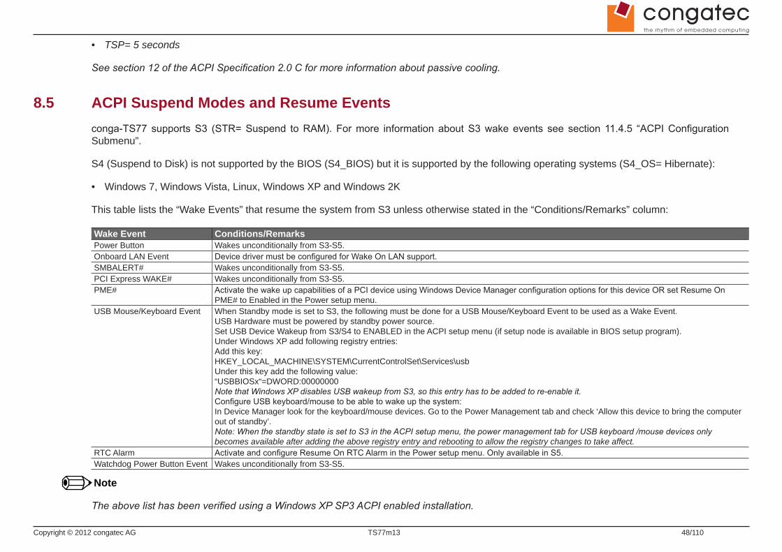
Copyright © 2012 congatec AG TS77m13 48/110
• TSP= 5 seconds
See section 12 of the ACPI Specification 2.0 C for more information about passive cooling.
8.5 ACPI Suspend Modes and Resume Eventsconga-TS77 supports S3 (STR= Suspend to RAM). For more information about S3 wake events see section 11.4.5 “ACPI Configuration Submenu”.
S4 (Suspend to Disk) is not supported by the BIOS (S4_BIOS) but it is supported by the following operating systems (S4_OS= Hibernate):
• Windows 7, Windows Vista, Linux, Windows XP and Windows 2K
This table lists the “Wake Events” that resume the system from S3 unless otherwise stated in the “Conditions/Remarks” column:
Wake Event Conditions/RemarksPower Button Wakes unconditionally from S3-S5.Onboard LAN Event Device driver must be configured for Wake On LAN support.SMBALERT# Wakes unconditionally from S3-S5.PCI Express WAKE# Wakes unconditionally from S3-S5.PME# Activate the wake up capabilities of a PCI device using Windows Device Manager configuration options for this device OR set Resume On
PME# to Enabled in the Power setup menu.USB Mouse/Keyboard Event When Standby mode is set to S3, the following must be done for a USB Mouse/Keyboard Event to be used as a Wake Event.
USB Hardware must be powered by standby power source. Set USB Device Wakeup from S3/S4 to ENABLED in the ACPI setup menu (if setup node is available in BIOS setup program).Under Windows XP add following registry entries:Add this key:HKEY_LOCAL_MACHINE\SYSTEM\CurrentControlSet\Services\usbUnder this key add the following value:“USBBIOSx“=DWORD:00000000Note that Windows XP disables USB wakeup from S3, so this entry has to be added to re-enable it.Configure USB keyboard/mouse to be able to wake up the system:In Device Manager look for the keyboard/mouse devices. Go to the Power Management tab and check ‘Allow this device to bring the computer out of standby’. Note: When the standby state is set to S3 in the ACPI setup menu, the power management tab for USB keyboard /mouse devices only becomes available after adding the above registry entry and rebooting to allow the registry changes to take affect.
RTC Alarm Activate and configure Resume On RTC Alarm in the Power setup menu. Only available in S5.Watchdog Power Button Event Wakes unconditionally from S3-S5.
Note
The above list has been verified using a Windows XP SP3 ACPI enabled installation.

Copyright © 2012 congatec AG TS77m13 49/110
8.6 USB 2.0 EHCI Host Controller SupportThe 8 available USB ports are provided by two USB 2.0 Rate Matching Hubs (RMH) integrated within the Intel® BD82QM77 or BD82HM76 (QM77 or HM76) PCH. Each EHCI controller has one hub connected to it as shown below. The Hubs convert low and full-speed traffic into high-speed traffic. When the RMHs are enabled, they will appear to software like an external hub is connected to Port 0 of each EHCI controller. In addition, port 1 of each of the RMHs is muxed with Port 1 of the EHCI controllers and is able to bypass the RMH for use as the Debug Port. The hub operates like any USB 2.0 Discrete Hub and will consume one tier of hubs allowed by the USB 2.0 Spec. A maximum of four additional non-root hubs can be supported on any of the PCH USB Ports. The RMH will report the following Vendor ID = 8087h and Product ID = 0024h.
Routing Diagram
EHCI #1 EHCI #2EHCI #1
Port 5Port 4Port 3Port 2Port 1Port 0Internal Port:
EHCI #2
Port 11 Port 12 Port 13Port 10Port 9Port 8
Ports 6-7 and 10-13Not supported on the conga-TS77
Port 7Port 6
Port 5Port 4Port 3Port 2Port 1Port 0COM Express Port: Unused Unused UnusedUnusedPort 7Port 6UnusedUnused
USB 2.0 Rate Matching HubUSB 2.0 Rate Matching Hub
EHCI #1 EHCI #2

Copyright © 2012 congatec AG TS77m13 50/110
9 Signal Descriptions and Pinout TablesThe following section describes the signals found on COM Express™ Type VI connectors used for congatec AG modules. The pinout of the modules complies with COM Express Type 6 Rev. 2.1.
Table 2 describes the terminology used in this section for the Signal Description tables. The PU/PD column indicates if a COM Express™ module pull-up or pull-down resistor has been used, if the field entry area in this column for the signal is empty, then no pull-up or pull-down resistor has been implemented by congatec.
The “#” symbol at the end of the signal name indicates that the active or asserted state occurs when the signal is at a low voltage level. When “#” is not present, the signal is asserted when at a high voltage level.
Note
The Signal Description tables do not list internal pull-ups or pull-downs implemented by the chip vendors, only pull-ups or pull-downs implemented by congatec are listed. For information about the internal pull-ups or pull-downs implemented by the chip vendors, refer to the respective chip’s datasheet.
Table 2 Signal Tables Terminology Descriptions
Term DescriptionPU congatec implemented pull-up resistorPD congatec implemented pull-down resistorI/O 3.3V Bi-directional signal 3.3V tolerantI/O 5V Bi-directional signal 5V tolerantI 3.3V Input 3.3V tolerantI 5V Input 5V tolerantI/O 3.3VSB Input 3.3V tolerant active in standby stateO 3.3V Output 3.3V signal levelO 5V Output 5V signal levelOD Open drain outputP Power Input/OutputDDC Display Data ChannelPCIE In compliance with PCI Express Base Specification, Revision 2.0PEG PCI Express GraphicsSATA In compliance with Serial ATA specification Revision 2.6 and 3.0.REF Reference voltage output. May be sourced from a module power plane.PDS Pull-down strap. A module output pin that is either tied to GND or is not connected. Used to signal
module capabilities (pinout type) to the Carrier Board.

Copyright © 2012 congatec AG TS77m13 51/110
9.1 A-B Connector Signal DescriptionsTable 3 Intel® High Definition Audio Link Signals Descriptions
Signal Pin # Description I/O PU/PD CommentAC/HDA_RST# A30 Intel® High Definition Audio Reset: This signal is the master hardware reset
to external codec(s).O 3.3VSB AC’97 codecs are not supported.
AC/HDA_SYNC A29 Intel® High Definition Audio Sync: This signal is a 48 kHz fixed rate sample sync to the codec(s). It is also used to encode the stream number.
O 3.3VSB PU 1K 3.3VSB
AC’97 codecs are not supported.AC/HDA_SYNC is a boot strap signal (see note below)
AC/HDA_BITCLK A32 Intel® High Definition Audio Bit Clock Output: This signal is a 24.000MHz serial data clock generated by the Intel® High Definition Audio controller.
O 3.3VSB AC’97 codecs are not supported.
AC/HDA_SDOUT A33 Intel® High Definition Audio Serial Data Out: This signal is the serial TDM data output to the codec(s). This serial output is double-pumped for a bit rate of 48 Mb/s for Intel® High Definition Audio.
O 3.3VSB PU 1K 3.3VSB
AC’97 codecs are not supported.AC/HDA_SDOUT is a boot strap signal (see note below)
AC/HDA_SDIN[2:0] B28-B30 Intel® High Definition Audio Serial Data In [0]: These signals are serial TDM data inputs from the three codecs. The serial input is single-pumped for a bit rate of 24 Mb/s for Intel® High Definition Audio.
I 3.3VSB AC’97 codecs are not supported.
Note
Some signals have special functionality during the reset process. They may bootstrap some basic important functions of the module.
For more information refer to section 9.5 of this user’s guide.

Copyright © 2012 congatec AG TS77m13 52/110
Table 4 Gigabit Ethernet Signal Descriptions
Gigabit Ethernet Pin # Description I/O PU/PD CommentGBE0_MDI0+GBE0_MDI0-GBE0_MDI1+GBE0_MDI1-GBE0_MDI2+GBE0_MDI2-GBE0_MDI3+GBE0_MDI3-
A13A12A10A9A7A6A3A2
Gigabit Ethernet Controller 0: Media Dependent Interface Differential Pairs 0, 1, 2, 3. The MDI can operate in 1000, 100, and 10Mbit/sec modes. Some pairs are unused in some modes according to the following:
I/O Analog Twisted pair signals for external transformer.
1000 100 10
MDI[0]+/- B1_DA+/- TX+/- TX+/-MDI[1]+/- B1_DB+/- RX+/- RX+/-MDI[2]+/- B1_DC+/-MDI[3]+/- B1_DD+/-
GBE0_ACT# B2 Gigabit Ethernet Controller 0 activity indicator, active low. O 3.3VSBGBE0_LINK# A8 Gigabit Ethernet Controller 0 link indicator, active low. O 3.3VSBGBE0_LINK100# A4 Gigabit Ethernet Controller 0 100Mbit/sec link indicator, active low. O 3.3VSBGBE0_LINK1000# A5 Gigabit Ethernet Controller 0 1000Mbit/sec link indicator, active low. O 3.3VSBGBE0_CTREF A14 Reference voltage for Carrier Board Ethernet channel 0 magnetics center tap. The reference voltage is
determined by the requirements of the module PHY and may be as low as 0V and as high as 3.3V. The reference voltage output shall be current limited on the module. In the case in which the reference is shorted to ground, the current shall be limited to 250mA or less.
Not connected
Note
The GBE0_LINK# output is only active during a 100Mbit or 1Gbit connection, it is not active during a 10Mbit connection. This is a limitation of Ethernet controller since it only has 3 LED outputs, ACT#, LINK100# and LINK1000#. The GBE0_LINK# signal is a logic AND of the GBE0_LINK100# and GBE0_LINK1000# signals on the conga-TS77 module.
Table 5 Serial ATA Signal Descriptions
Signal Pin # Description I/O PU/PD CommentSATA0_RX+ SATA0_RX-
A19A20
Serial ATA channel 0, Receive Input differential pair. I SATA Supports Serial ATA specification, Revision 3.0
SATA0_TX+ SATA0_TX-
A16A17
Serial ATA channel 0, Transmit Output differential pair. O SATA Supports Serial ATA specification, Revision 3.0
SATA1_RX+ SATA1_RX-
B19B20
Serial ATA channel 1, Receive Input differential pair. I SATA Supports Serial ATA specification, Revision 3.0
SATA1_TX+ SATA1_TX-
B16B17
Serial ATA channel 1, Transmit Output differential pair. O SATA Supports Serial ATA specification, Revision 3.0
SATA2_RX+ SATA2_RX-
A25A26
Serial ATA channel 2, Receive Input differential pair. I SATA Supports Serial ATA specification, Revision 2.6
SATA2_TX+ SATA2_TX-
A22A23
Serial ATA channel 2, Transmit Output differential pair. O SATA Supports Serial ATA specification, Revision 2.6
SATA3_RX+ SATA3_RX-
B25B26
Serial ATA channel 3, Receive Input differential pair. I SATA Supports Serial ATA specification, Revision 2.6

Copyright © 2012 congatec AG TS77m13 53/110
Signal Pin # Description I/O PU/PD CommentSATA3_TX+ SATA3_TX-
B22B23
Serial ATA channel 3, Transmit Output differential pair. O SATA Supports Serial ATA specification, Revision 2.6
(S)ATA_ACT# A28 ATA (parallel and serial) or SAS activity indicator, active low. I/O 3.3v
Table 6 PCI Express Signal Descriptions (general purpose)
Signal Pin # Description I/O PU/PD CommentPCIE_RX0+ PCIE_RX0-
B68B69
PCI Express channel 0, Receive Input differential pair. I PCIE Supports PCI Express Base Specification, Revision 2.0
PCIE_TX0+ PCIE_TX0-
A68A69
PCI Express channel 0, Transmit Output differential pair. O PCIE Supports PCI Express Base Specification, Revision 2.0
PCIE_RX1+ PCIE_RX1-
B64B65
PCI Express channel 1, Receive Input differential pair. I PCIE Supports PCI Express Base Specification, Revision 2.0
PCIE_TX1+ PCIE_TX1-
A64A65
PCI Express channel 1, Transmit Output differential pair. O PCIE Supports PCI Express Base Specification, Revision 2.0
PCIE_RX2+ PCIE_RX2-
B61B62
PCI Express channel 2, Receive Input differential pair. I PCIE Supports PCI Express Base Specification, Revision 2.0
PCIE_TX2+ PCIE_TX2-
A61A62
PCI Express channel 2, Transmit Output differential pair. O PCIE Supports PCI Express Base Specification, Revision 2.0
PCIE_RX3+ PCIE_RX3-
B58B59
PCI Express channel 3, Receive Input differential pair. I PCIE Supports PCI Express Base Specification, Revision 2.0
PCIE_TX3+ PCIE_TX3-
A58A59
PCI Express channel 3, Transmit Output differential pair. O PCIE Supports PCI Express Base Specification, Revision 2.0
PCIE_RX4+ PCIE_RX4-
B55B56
PCI Express channel 4, Receive Input differential pair. I PCIE Supports PCI Express Base Specification, Revision 2.0
PCIE_TX4+ PCIE_TX4-
A55A56
PCI Express channel 4, Transmit Output differential pair. O PCIE Supports PCI Express Base Specification, Revision 2.0
PCIE_RX5+ PCIE_RX5-
B52B53
PCI Express channel 5, Receive Input differential pair. I PCIE Supports PCI Express Base Specification, Revision 2.0
PCIE_TX5+ PCIE_TX5-
A52A53
PCI Express channel 5, Transmit Output differential pair. O PCIE Supports PCI Express Base Specification, Revision 2.0
PCIE_CLK_REF+ PCIE_CLK_REF-
A88A89
PCI Express Reference Clock output for all PCI Express and PCI Express Graphics Lanes.
O PCIE A PCI Express Gen2/3 compliant clock buffer chip must be used on the carrier board if more than one PCI Express device is designed in.
Table 7 ExpressCard Support Pins Signal Descriptions
Signal Pin # Description I/O PU/PD CommentEXCD0_CPPE#EXCD1_CPPE#
A49B48
ExpressCard capable card request. I 3.3V PU 10k 3.3V
EXCD0_PERST#EXCD1_PERST#
A48B47
ExpressCard Reset O 3.3V PU 10k 3.3V

Copyright © 2012 congatec AG TS77m13 54/110
Table 8 LPC Signal Descriptions
Signal Pin # Description I/O PU/PD CommentLPC_AD[0:3] B4-B7 LPC multiplexed address, command and data bus I/O 3.3VLPC_FRAME# B3 LPC frame indicates the start of an LPC cycle O 3.3VLPC_DRQ[0:1]# B8-B9 LPC serial DMA request I 3.3VLPC_SERIRQ A50 LPC serial interrupt I/O OD 3.3V PU 10k 3.3VLPC_CLK B10 LPC clock output - 33MHz nominal O 3.3V
Table 9 USB Signal Descriptions
Signal Pin # Description I/O PU/PD CommentUSB0+ A46 USB Port 0, data + or D+ I/O USB 2.0 compliant. Backwards compatible to USB 1.1USB0- A45 USB Port 0, data - or D- I/O USB 2.0 compliant. Backwards compatible to USB 1.1USB1+ B46 USB Port 1, data + or D+ I/O USB 2.0 compliant. Backwards compatible to USB 1.1USB1- B45 USB Port 1, data - or D- I/O USB 2.0 compliant. Backwards compatible to USB 1.1USB2+ A43 USB Port 2, data + or D+ I/O USB 2.0 compliant. Backwards compatible to USB 1.1USB2- A42 USB Port 2, data - or D- I/O USB 2.0 compliant. Backwards compatible to USB 1.1USB3+ B43 USB Port 3, data + or D+ I/O USB 2.0 compliant. Backwards compatible to USB 1.1USB3- B42 USB Port 3, data - or D- I/O USB 2.0 compliant. Backwards compatible to USB 1.1USB4+ A40 USB Port 4, data + or D+ I/O USB 2.0 compliant. Backwards compatible to USB 1.1USB4- A39 USB Port 4, data - or D- I/O USB 2.0 compliant. Backwards compatible to USB 1.1USB5+ B40 USB Port 5, data + or D+ I/O USB 2.0 compliant. Backwards compatible to USB 1.1USB5- B39 USB Port 5, data - or D- I/O USB 2.0 compliant. Backwards compatible to USB 1.1USB6+ A37 USB Port 6, data + or D+ I/O USB 2.0 compliant. Backwards compatible to USB 1.1USB6- A36 USB Port 6, data - or D- I/O USB 2.0 compliant. Backwards compatible to USB 1.1USB7+ B37 USB Port 7, data + or D+ I/O USB 2.0 compliant. Backwards compatible to USB 1.1USB7- B36 USB Port 7, data - or D- I/O USB 2.0 compliant. Backwards compatible to USB 1.1USB_0_1_OC# B44 USB over-current sense, USB ports 0 and 1. A pull-up for this line shall
be present on the module. An open drain driver from a USB current monitor on the carrier board may drive this line low.
I 3.3VSB
PU 10k 3.3VSB
Do not pull this line high on the carrier board.
USB_2_3_OC# A44 USB over-current sense, USB ports 2 and 3. A pull-up for this line shall be present on the module. An open drain driver from a USB current monitor on the carrier board may drive this line low. .
I 3.3VSB
PU 10k 3.3VSB
Do not pull this line high on the carrier board.
USB_4_5_OC# B38 USB over-current sense, USB ports 4 and 5. A pull-up for this line shall be present on the module. An open drain driver from a USB current monitor on the carrier board may drive this line low.
I 3.3VSB
PU 10k 3.3VSB
Do not pull this line high on the carrier board.
USB_6_7_OC# A38 USB over-current sense, USB ports 6 and 7. A pull-up for this line shall be present on the module. An open drain driver from a USB current monitor on the carrier board may drive this line low.
I 3.3VSB
PU 10k 3.3VSB
Do not pull this line high on the carrier board.

Copyright © 2012 congatec AG TS77m13 55/110
Table 10 CRT Signal Descriptions
Signal Pin # Description I/O PU/PD CommentVGA_RED B89 Red for monitor. Analog DAC output, designed to drive a 37.5-Ohm equivalent load. O Analog PD 150R Analog outputVGA_GRN B91 Green for monitor. Analog DAC output, designed to drive a 37.5-Ohm equivalent load. O Analog PD 150R Analog outputVGA_BLU B92 Blue for monitor. Analog DAC output, designed to drive a 37.5-Ohm equivalent load. O Analog PD 150R Analog outputVGA_HSYNC B93 Horizontal sync output to VGA monitor O 3.3VVGA_VSYNC B94 Vertical sync output to VGA monitor O 3.3VVGA_I2C_CK B95 DDC clock line (I²C port dedicated to identify VGA monitor capabilities) I/O OD 5V PU 2k2 3.3VVGA_I2C_DAT B96 DDC data line. I/O OD 5V PU 2k2 3.3V
Table 11 LVDS Signal Descriptions
Signal Pin # Description I/O PU/PD CommentLVDS_A0+ LVDS_A0- LVDS_A1+LVDS_A1- LVDS_A2+LVDS_A2- LVDS_A3+LVDS_A3-
A71A72A73A74A75A76A78A79
LVDS Channel A differential pairs O LVDS
LVDS_A_CK+ LVDS_A_CK-
A81A82
LVDS Channel A differential clock O LVDS
LVDS_B0+ LVDS_B0- LVDS_B1+LVDS_B1- LVDS_B2+LVDS_B2- LVDS_B3+LVDS_B3-
B71B72B73B74B75B76B77B78
LVDS Channel B differential pairs O LVDS
LVDS_B_CK+ LVDS_B_CK-
B81B82
LVDS Channel B differential clock O LVDS
LVDS_VDD_EN A77 LVDS panel power enable O 3.3V PD 10kLVDS_BKLT_EN B79 LVDS panel backlight enable O 3.3V PD 10kLVDS_BKLT_CTRL B83 LVDS panel backlight brightness control O 3.3VLVDS_I2C_CK A83 DDC lines used for flat panel detection and control. O 3.3V PU 2k2 3.3VLVDS_I2C_DAT A84 DDC lines used for flat panel detection and control. I/O 3.3V PU 2k2 3.3V LVDS_I2C_DAT is a boot strap signal (see note below).
Note
Some signals have special functionality during the reset process. They may bootstrap some basic important functions of the module. For more information refer to section 9.5 of this user’s guide.

Copyright © 2012 congatec AG TS77m13 56/110
Table 12 SPI BIOS Flash Interface Signal Descriptions
Signal Pin # Description I/O PU/PD CommentSPI_CS# B97 Chip select for Carrier Board SPI BIOS Flash. O 3.3VSB Carrier shall pull to SPI_POWER when
external SPI provided but not used.SPI_MISO A92 Data in to module from carrier board SPI BIOS flash. I 3.3VSBSPI_MOSI A95 Data out from module to carrier board SPI BIOS flash. O 3.3VSBSPI_CLK A94 Clock from module to carrier board SPI BIOS flash. O 3.3VSBSPI_POWER A91 Power source for carrier board SPI BIOS flash. SPI_POWER shall be used to power
SPI BIOS flash on the carrier only.+ 3.3VSB
BIOS_DIS0# A34 Selection strap to determine the BIOS boot device. I 3.3VSB PU 10K 3.3VSB
Carrier shall pull to GND or leave no-connect.
BIOS_DIS1# B88 Selection strap to determine the BIOS boot device. I 3.3VSB PU 10K 3.3VSB
Carrier shall pull to GND or leave no-connect
Table 13 Miscellaneous Signal Descriptions
Signal Pin # Description I/O PU/PD CommentI2C_CK B33 General purpose I²C port clock output/input I/O 3.3V PU 2K2 3.3VSBI2C_DAT B34 General purpose I²C port data I/O line I/O 3.3V PU 2K2 3.3VSBSPKR B32 Output for audio enunciator, the “speaker” in PC-AT systems O 3.3V SPEAKER is a boot strap signal
(see note below)WDT B27 Output indicating that a watchdog time-out event has occurred. O 3.3VFAN_PWMOUT B101 Fan speed control. Uses the Pulse Width Modulation (PWM) technique to control
the fan’s RPM.O OD 3.3V
PU 10K 3.3V
FAN_TACHIN B102 Fan tachometer input. I OD PU 10K 3.3V Requires a fan with a two pulse output.
TPM_PP A96 Physical Presence pin of Trusted Platform Module (TPM). Active high. TPM chip has an internal pull-down. This signal is used to indicate Physical Presence to the TPM.
I 3.3V Trusted Platform Module chip is optional.
Note
Some signals have special functionality during the reset process. They may bootstrap some basic important functions of the module. For more information refer to section 9.5 of this user’s guide.

Copyright © 2012 congatec AG TS77m13 57/110
Table 14 General Purpose I/O Signal Descriptions
Signal Pin # Description I/O PU/PD CommentGPO0 A93 General purpose output pins.
Shared with SD_CLK. Output from COM Express, input to SDO 3.3V SDIO interface is not supported on the conga-TS77
GPO1 B54 General purpose output pins.Shared with SD_CMD. Output from COM Express, input to SD
O 3.3V SDIO interface is not supported on the conga-TS77
GPO2 B57 General purpose output pins.Shared with SD_WP. Output from COM Express, input to SD
O 3.3V SDIO interface is not supported on the conga-TS77
GPO3 B63 General purpose output pins. Shared with SD_CD. Output from COM Express, input to SD
O 3.3V SDIO interface is not supported on the conga-TS77
GPI0 A54 General purpose input pins. Pulled high internally on the module. Shared with SD_DATA0. Bidirectional signal
I 3.3V PU 10K 3.3V SDIO interface is not supported on the conga-TS77
GPI1 A63 General purpose input pins. Pulled high internally on the module. Shared with SD_DATA1. Bidirectional signal
I 3.3V PU 10K 3.3V SDIO interface is not supported on the conga-TS77
GPI2 A67 General purpose input pins. Pulled high internally on the module. Shared with SD_DATA2. Bidirectional signal
I 3.3V PU 10K 3.3V SDIO interface is not supported on the conga-TS77
GPI3 A85 General purpose input pins. Pulled high internally on the module. Shared with SD_DATA3. Bidirectional signal.
I 3.3V PU 10K 3.3V SDIO interface is not supported on the conga-TS77
Table 15 Power and System Management Signal Descriptions
Signal Pin # Description I/O PU/PD CommentPWRBTN# B12 Power button to bring system out of S5 (soft off), active on rising edge. I 3.3VSB PU 10k 3.3VSBSYS_RESET# B49 Reset button input. Active low input. Edge triggered.
System will not be held in hardware reset while this input is kept low.I 3.3VSB PU 10k 3.3VSB
CB_RESET# B50 Reset output from module to Carrier Board. Active low. Issued by module chipset and may result from a low SYS_RESET# input, a low PWR_OK input, a VCC_12V power input that falls below the minimum specification, a watchdog timeout, or may be initiated by the module software.
O 3.3V PD 100k
PWR_OK B24 Power OK from main power supply. A high value indicates that the power is good. I 3.3V Set by resistor divider to accept 3.3V.
SUS_STAT# B18 Indicates imminent suspend operation; used to notify LPC devices. O 3.3VSB PU 10k 3.3VSBSUS_S3# A15 Indicates system is in Suspend to RAM state. Active-low output. An inverted copy of SUS_S3#
on the carrier board (also known as “PS_ON”) may be used to enable the non-standby power on a typical ATX power supply.
O 3.3VSB
SUS_S4# A18 Indicates system is in Suspend to Disk state. Active low output. O 3.3VSB Not supportedSUS_S5# A24 Indicates system is in Soft Off state. O 3.3VSBWAKE0# B66 PCI Express wake up signal. I 3.3VSB PU 1k 3.3VSBWAKE1# B67 General purpose wake up signal. May be used to implement wake-up on PS/2 keyboard or
mouse activity. I 3.3VSB PU 10k 3.3VSB
BATLOW# A27 Battery low input. This signal may be driven low by external circuitry to signal that the system battery is low, or may be used to signal some other external power-management event.
I 3.3VSB PU 10k 3.3VSB
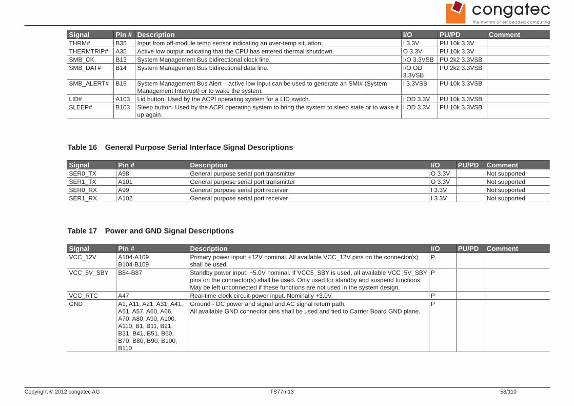
Copyright © 2012 congatec AG TS77m13 58/110
Signal Pin # Description I/O PU/PD CommentTHRM# B35 Input from off-module temp sensor indicating an over-temp situation. I 3.3V PU 10k 3.3VTHERMTRIP# A35 Active low output indicating that the CPU has entered thermal shutdown. O 3.3V PU 10k 3.3VSMB_CK B13 System Management Bus bidirectional clock line. I/O 3.3VSB PU 2k2 3.3VSBSMB_DAT# B14 System Management Bus bidirectional data line. I/O OD
3.3VSBPU 2k2 3.3VSB
SMB_ALERT# B15 System Management Bus Alert – active low input can be used to generate an SMI# (System Management Interrupt) or to wake the system.
I 3.3VSB PU 10k 3.3VSB
LID# A103 Lid button. Used by the ACPI operating system for a LID switch. I OD 3.3V PU 10k 3.3VSB SLEEP# B103 Sleep button. Used by the ACPI operating system to bring the system to sleep state or to wake it
up again.I OD 3.3V PU 10k 3.3VSB
Table 16 General Purpose Serial Interface Signal Descriptions
Signal Pin # Description I/O PU/PD CommentSER0_TX A98 General purpose serial port transmitter O 3.3V Not supportedSER1_TX A101 General purpose serial port transmitter O 3.3V Not supportedSER0_RX A99 General purpose serial port receiver I 3.3V Not supportedSER1_RX A102 General purpose serial port receiver I 3.3V Not supported
Table 17 Power and GND Signal Descriptions
Signal Pin # Description I/O PU/PD CommentVCC_12V A104-A109
B104-B109Primary power input: +12V nominal. All available VCC_12V pins on the connector(s) shall be used.
P
VCC_5V_SBY B84-B87 Standby power input: +5.0V nominal. If VCC5_SBY is used, all available VCC_5V_SBY pins on the connector(s) shall be used. Only used for standby and suspend functions. May be left unconnected if these functions are not used in the system design.
P
VCC_RTC A47 Real-time clock circuit-power input. Nominally +3.0V. PGND A1, A11, A21, A31, A41,
A51, A57, A60, A66, A70, A80, A90, A100, A110, B1, B11, B21, B31, B41, B51, B60, B70, B80, B90, B100, B110
Ground - DC power and signal and AC signal return path. All available GND connector pins shall be used and tied to Carrier Board GND plane.
P

Copyright © 2012 congatec AG TS77m13 59/110
9.2 A-B Connector PinoutTable 18 Connector A-B Pinout
Pin Row A Pin Row B Pin Row A Pin Row BA1 GND (FIXED) B1 GND (FIXED) A56 PCIE_TX4- B56 PCIE_RX4- A2 GBE0_MDI3- B2 GBE0_ACT# A57 GND B57 GPO2 A3 GBE0_MDI3+ B3 LPC_FRAME# A58 PCIE_TX3+ B58 PCIE_RX3+ A4 GBE0_LINK100# B4 LPC_AD0 A59 PCIE_TX3- B59 PCIE_RX3- A5 GBE0_LINK1000# B5 LPC_AD1 A60 GND (FIXED) B60 GND (FIXED)A6 GBE0_MDI2- B6 LPC_AD2 A61 PCIE_TX2+ B61 PCIE_RX2+ A7 GBE0_MDI2+ B7 LPC_AD3 A62 PCIE_TX2- B62 PCIE_RX2- A8 GBE0_LINK# B8 LPC_DRQ0# A63 GPI1 B63 GPO3 A9 GBE0_MDI1- B9 LPC_DRQ1# A64 PCIE_TX1+ B64 PCIE_RX1+A10 GBE0_MDI1+ B10 LPC_CLK A65 PCIE_TX1- B65 PCIE_RX1- A11 GND (FIXED) B11 GND (FIXED) A66 GND B66 WAKE0# A12 GBE0_MDI0- B12 PWRBTN# A67 GPI2 B67 WAKE1# A13 GBE0_MDI0+ B13 SMB_CK A68 PCIE_TX0+ B68 PCIE_RX0+A14 GBE0_CTREF (*) B14 SMB_DAT A69 PCIE_TX0- B69 PCIE_RX0- A15 SUS_S3# B15 SMB_ALERT# A70 GND (FIXED) B70 GND (FIXED)A16 SATA0_TX+ B16 SATA1_TX+ A71 LVDS_A0+ B71 LVDS_B0+ A17 SATA0_TX- B17 SATA1_TX- A72 LVDS_A0- B72 LVDS_B0- A18 SUS_S4# B18 SUS_STAT# A73 LVDS_A1+ B73 LVDS_B1+ A19 SATA0_RX+ B19 SATA1_RX+ A74 LVDS_A1- B74 LVDS_B1- A20 SATA0_RX- B20 SATA1_RX- A75 LVDS_A2+ B75 LVDS_B2+ A21 GND (FIXED) B21 GND (FIXED) A76 LVDS_A2- B76 LVDS_B2- A22 SATA2_TX+ B22 SATA3_TX+ A77 LVDS_VDD_EN B77 LVDS_B3+ A23 SATA2_TX- B23 SATA3_TX- A78 LVDS_A3+ B78 LVDS_B3- A24 SUS_S5# B24 PWR_OK A79 LVDS_A3- B79 LVDS_BKLT_ENA25 SATA2_RX+ B25 SATA3_RX+ A80 GND (FIXED) B80 GND (FIXED)A26 SATA2_RX- B26 SATA3_RX- A81 LVDS_A_CK+ B81 LVDS_B_CK+ A27 BATLOW# B27 WDT A82 LVDS_A_CK- B82 LVDS_B_CK- A28 (S)ATA_ACT# B28 AC/HDA_SDIN2 A83 LVDS_I2C_CK B83 LVDS_BKLT_CTRL A29 AC/HDA_SYNC B29 AC/HDA_SDIN1 A84 LVDS_I2C_DAT B84 VCC_5V_SBY A30 AC/HDA_RST# B30 AC/HDA_SDIN0 A85 GPI3 B85 VCC_5V_SBY A31 GND (FIXED) B31 GND (FIXED) A86 RSVD B86 VCC_5V_SBY A32 AC/HDA_BITCLK B32 SPKR A87 RSVD B87 VCC_5V_SBY A33 AC/HDA_SDOUT B33 I2C_CK A88 PCIE0_CK_REF+ B88 BIOS_DIS1# A34 BIOS_DIS0# B34 I2C_DAT A89 PCIE0_CK_REF- B89 VGA_RED A35 THRMTRIP# B35 THRM# A90 GND (FIXED) B90 GND (FIXED) A36 USB6- B36 USB7- A91 SPI_POWER B91 VGA_GRN A37 USB6+ B37 USB7+ A92 SPI_MISO B92 VGA_BLU
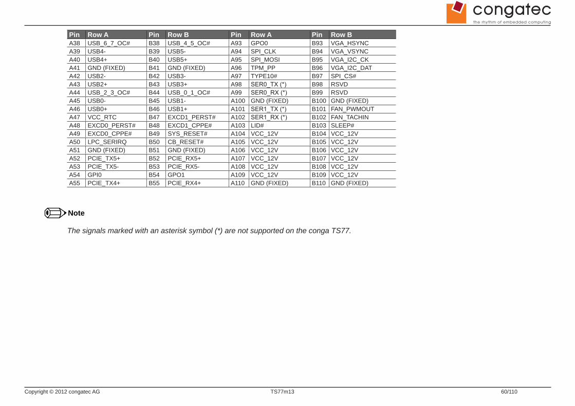
Copyright © 2012 congatec AG TS77m13 60/110
Pin Row A Pin Row B Pin Row A Pin Row BA38 USB_6_7_OC# B38 USB_4_5_OC# A93 GPO0 B93 VGA_HSYNC A39 USB4- B39 USB5- A94 SPI_CLK B94 VGA_VSYNC A40 USB4+ B40 USB5+ A95 SPI_MOSI B95 VGA_I2C_CK A41 GND (FIXED) B41 GND (FIXED) A96 TPM_PP B96 VGA_I2C_DAT A42 USB2- B42 USB3- A97 TYPE10# B97 SPI_CS#A43 USB2+ B43 USB3+ A98 SER0_TX (*) B98 RSVDA44 USB_2_3_OC# B44 USB_0_1_OC# A99 SER0_RX (*) B99 RSVDA45 USB0- B45 USB1- A100 GND (FIXED) B100 GND (FIXED) A46 USB0+ B46 USB1+ A101 SER1_TX (*) B101 FAN_PWMOUT A47 VCC_RTC B47 EXCD1_PERST# A102 SER1_RX (*) B102 FAN_TACHINA48 EXCD0_PERST# B48 EXCD1_CPPE# A103 LID# B103 SLEEP# A49 EXCD0_CPPE# B49 SYS_RESET# A104 VCC_12V B104 VCC_12V A50 LPC_SERIRQ B50 CB_RESET# A105 VCC_12V B105 VCC_12V A51 GND (FIXED) B51 GND (FIXED) A106 VCC_12V B106 VCC_12V A52 PCIE_TX5+ B52 PCIE_RX5+ A107 VCC_12V B107 VCC_12V A53 PCIE_TX5- B53 PCIE_RX5- A108 VCC_12V B108 VCC_12V A54 GPI0 B54 GPO1 A109 VCC_12V B109 VCC_12V A55 PCIE_TX4+ B55 PCIE_RX4+ A110 GND (FIXED) B110 GND (FIXED)
Note
The signals marked with an asterisk symbol (*) are not supported on the conga TS77.
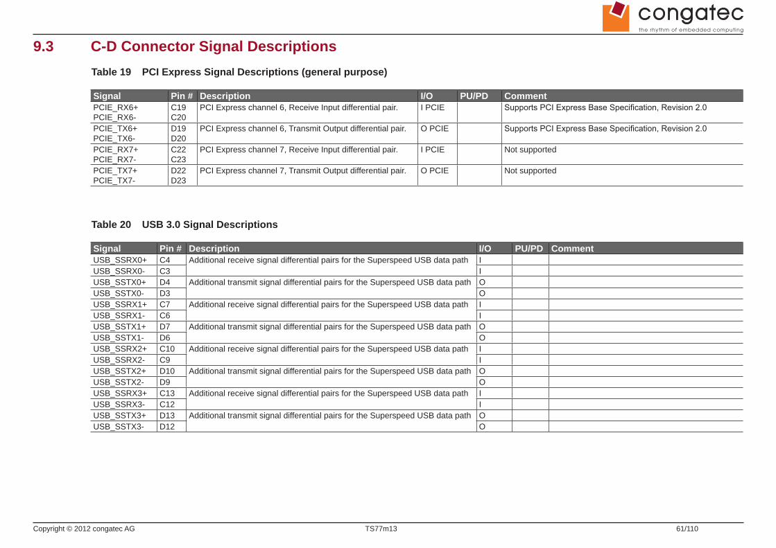
Copyright © 2012 congatec AG TS77m13 61/110
9.3 C-D Connector Signal DescriptionsTable 19 PCI Express Signal Descriptions (general purpose)
Signal Pin # Description I/O PU/PD CommentPCIE_RX6+ PCIE_RX6-
C19C20
PCI Express channel 6, Receive Input differential pair. I PCIE Supports PCI Express Base Specification, Revision 2.0
PCIE_TX6+ PCIE_TX6-
D19D20
PCI Express channel 6, Transmit Output differential pair. O PCIE Supports PCI Express Base Specification, Revision 2.0
PCIE_RX7+ PCIE_RX7-
C22C23
PCI Express channel 7, Receive Input differential pair. I PCIE Not supported
PCIE_TX7+ PCIE_TX7-
D22D23
PCI Express channel 7, Transmit Output differential pair. O PCIE Not supported
Table 20 USB 3.0 Signal Descriptions
Signal Pin # Description I/O PU/PD CommentUSB_SSRX0+ C4 Additional receive signal differential pairs for the Superspeed USB data path IUSB_SSRX0- C3 IUSB_SSTX0+ D4 Additional transmit signal differential pairs for the Superspeed USB data path OUSB_SSTX0- D3 OUSB_SSRX1+ C7 Additional receive signal differential pairs for the Superspeed USB data path IUSB_SSRX1- C6 IUSB_SSTX1+ D7 Additional transmit signal differential pairs for the Superspeed USB data path OUSB_SSTX1- D6 OUSB_SSRX2+ C10 Additional receive signal differential pairs for the Superspeed USB data path IUSB_SSRX2- C9 IUSB_SSTX2+ D10 Additional transmit signal differential pairs for the Superspeed USB data path OUSB_SSTX2- D9 OUSB_SSRX3+ C13 Additional receive signal differential pairs for the Superspeed USB data path IUSB_SSRX3- C12 IUSB_SSTX3+ D13 Additional transmit signal differential pairs for the Superspeed USB data path OUSB_SSTX3- D12 O

Copyright © 2012 congatec AG TS77m13 62/110
Table 21 PCI Express Signal Descriptions (x16 Graphics)
Signal Pin # Description I/O PU/PD CommentPEG_RX0+PEG_RX0-PEG_RX1+PEG_RX1-PEG_RX2+PEG_RX2-PEG_RX3+PEG_RX3-PEG_RX4+PEG_RX4-PEG_RX5+PEG_RX5-PEG_RX6+PEG_RX6-PEG_RX7+PEG_RX7-PEG_RX8+PEG_RX8-PEG_RX9+PEG_RX9-PEG_RX10+PEG_RX10-PEG_RX11+PEG_RX11-PEG_RX12+PEG_RX12-PEG_RX13+PEG_RX13-PEG_RX14+PEG_RX14-PEG_RX15+PEG_RX15-
C52C53C55C56C58C59C61C62C65C66C68C69C71C72C74C75C78C79C81C82C85C86C88C89C91C92C94C95C98C99C101C102
PCI Express Graphics Receive Input differential pairs. Note: Can also be used as PCI Express Receive Input differential pairs 16 through 31 known as PCIE_RX[16-31] + and -.
I PCIE
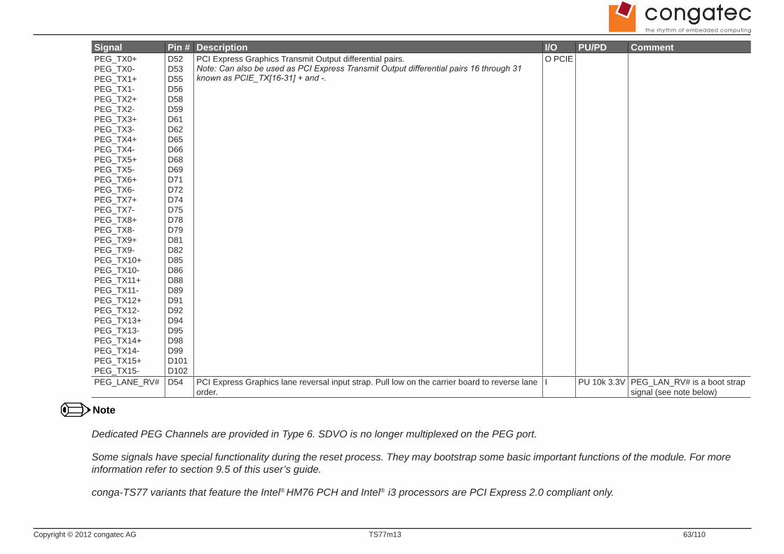
Copyright © 2012 congatec AG TS77m13 63/110
Signal Pin # Description I/O PU/PD CommentPEG_TX0+PEG_TX0-PEG_TX1+PEG_TX1-PEG_TX2+PEG_TX2-PEG_TX3+PEG_TX3-PEG_TX4+PEG_TX4-PEG_TX5+PEG_TX5-PEG_TX6+PEG_TX6-PEG_TX7+PEG_TX7-PEG_TX8+PEG_TX8-PEG_TX9+PEG_TX9-PEG_TX10+PEG_TX10-PEG_TX11+PEG_TX11-PEG_TX12+PEG_TX12-PEG_TX13+PEG_TX13-PEG_TX14+PEG_TX14-PEG_TX15+PEG_TX15-
D52D53D55D56D58D59D61D62D65D66D68D69D71D72D74D75D78D79D81D82D85D86D88D89D91D92D94D95D98D99D101D102
PCI Express Graphics Transmit Output differential pairs. Note: Can also be used as PCI Express Transmit Output differential pairs 16 through 31 known as PCIE_TX[16-31] + and -.
O PCIE
PEG_LANE_RV# D54 PCI Express Graphics lane reversal input strap. Pull low on the carrier board to reverse lane order.
I PU 10k 3.3V PEG_LAN_RV# is a boot strap signal (see note below)
Note
Dedicated PEG Channels are provided in Type 6. SDVO is no longer multiplexed on the PEG port.
Some signals have special functionality during the reset process. They may bootstrap some basic important functions of the module. For more information refer to section 9.5 of this user’s guide.
conga-TS77 variants that feature the Intel® HM76 PCH and Intel® i3 processors are PCI Express 2.0 compliant only.

Copyright © 2012 congatec AG TS77m13 64/110
Table 22 DDI Signal Description
Signal Pin # Description I/O PU/PD CommentDDI1_PAIR0+DDI1_PAIR0-
D26 D27
Multiplexed with SDVO1_RED+, DP1_LANE0+ and TMDS1_DATA2+.Multiplexed with SDVO1_RED-, DP1_LANE0- and TMDS1_DATA2-.
O PCIE
DDI1_PAIR1+DDI1_PAIR1-
D29 D30
Multiplexed with SDVO1_GRN+, DP1_LANE1+ and TMDS1_DATA1+.Multiplexed with SDVO1_GRN-, DP1_LANE1- and TMDS1_DATA1-.
O PCIE
DDI1_PAIR2+DDI1_PAIR2-
D32 D33
Multiplexed with SDVO1_BLU+, DP1_LANE2+ and TMDS1_DATA0+.Multiplexed with SDVO1_BLU-, DP1_LANE2- and TMDS1_DATA0-.
O PCIE
DDI1_PAIR3+DDI1_PAIR3-
D36 D37
Multiplexed with SDVO1_CK+, DP1_LANE3+ and TMDS1_CLK+.Multiplexed with SDVO1_CK-, DP1_LANE3- and TMDS1_CLK-.
O PCIE
DDI1_PAIR4+DDI1_PAIR4-
C25 C26
Multiplexed with SDVO1_INT+.Multiplexed with SDVO1_INT-.
DDI1_PAIR5+DDI1_PAIR5-
C29 C30
Multiplexed with SDVO1_TVCLKIN+.Multiplexed with SDVO1_TVCLKIN-.
DDI1_PAIR6+DDI1_PAIR6-
C15 C16
Multiplexed with SDVO1_FLDSTALL+.Multiplexed with SDVO1_FLDSTALL-.
DDI1_HPD C24 Multiplexed with DP1_HPD and HDMI1_HPD. I 3.3V PD 1MDDI1_CTRLCLK_AUX+ D15 Multiplexed with SDVO1_CTRLCLK, DP1_AUX+ and HMDI1_CTRLCLK.
DP AUX+ function if DDI1_DDC_AUX_SEL is no connect.HDMI/DVI I2C CTRLCLK if DDI1_DDC_AUX_SEL is pulled high
I/O PCIEI/O OD 3.3V
PD100k
DDI1_CTRLDATA_AUX- D16 Multiplexed with SDVO1_CTRLDATA, DP1_AUX- and HDMI1_CTRLDATA.DP AUX- function if DDI1_DDC_AUX_SEL is no connect.HDMI/DVI I2C CTRLDATA if DDI1_DDC_AUX_SEL is pulled high
I/O PCIEI/O OD 3.3V
PU 100k 3.3V
DDI1_CTRLDATA_AUX- is a boot strap signal (see not below).DDI enable strap already populated.
DDI1_DDC_AUX_SEL D34 Selects the function of DDI1_CTRLCLK_AUX+ and DDI1_CTRLDATA_AUX-. This pin shall have a IM pull-down to logic ground on the module. If this input is floating, the AUX pair is used for the DP AUX+/- signals. If pulled-high, the AUX pair contains the CTRLCLK and CTRLDATA signals.
I 3.3V PD 1M
DDI2_PAIR0+DDI2_PAIR0-
D39 D40
Multiplexed with DP2_LANE0+ and TMDS2_DATA2+.Multiplexed with DP2_LANE0- and TMDS2_DATA2-.
O PCIE
DDI2_PAIR1+DDI2_PAIR1-
D42 D43
Multiplexed with DP2_LANE1+ and TMDS2_DATA1+.Multiplexed with DP2_LANE1- and TMDS2_DATA1-.
O PCIE
DDI2_PAIR2+DDI2_PAIR2-
D46 D47
Multiplexed with DP2_LANE2+ and TMDS2_DATA0+.Multiplexed with DP2_LANE2- and TMDS2_DATA0-.
O PCIE
DDI2_PAIR3+DDI2_PAIR3-
D49 D50
Multiplexed with DP2_LANE3+ and TMDS2_CLK+.Multiplexed with DP2_LANE3- and TMDS2_CLK-.
O PCIE
DDI2_HPD D44 Multiplexed with DP2_HPD and HDMI2_HPD. I 3.3V PD 1MDDI2_CTRLCLK_AUX+ C32 Multiplexed with DP2_AUX+ and HDMI2_CTRLCLK.
DP AUX+ function if DDI2_DDC_AUX_SEL is no connect.HDMI/DVI I2C CTRLCLK if DDI2_DDC_AUX_SEL is pulled high
I/O PCIEI/O OD 3.3V
PD 100k
DDI2_CTRLDATA_AUX- C33 Multiplexed with DP2_AUX- and HDMI2_CTRLDATA.DP AUX- function if DDI2_DDC_AUX_SEL is no connect.HDMI/DVI I2C CTRLDATA if DDI2_DDC_AUX_SEL is pulled high.
I/O PCIEI/O OD 3.3V
PU 100k 3.3V
DDI2_CTRLCLK_AUX- is a boot strap signal (see note below).DDI enable strap already populated.
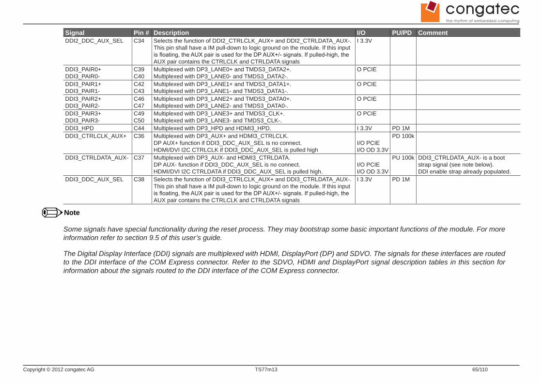
Copyright © 2012 congatec AG TS77m13 65/110
Signal Pin # Description I/O PU/PD CommentDDI2_DDC_AUX_SEL C34 Selects the function of DDI2_CTRLCLK_AUX+ and DDI2_CTRLDATA_AUX-.
This pin shall have a IM pull-down to logic ground on the module. If this input is floating, the AUX pair is used for the DP AUX+/- signals. If pulled-high, the AUX pair contains the CTRLCLK and CTRLDATA signals
I 3.3V
DDI3_PAIR0+DDI3_PAIR0-
C39 C40
Multiplexed with DP3_LANE0+ and TMDS3_DATA2+.Multiplexed with DP3_LANE0- and TMDS3_DATA2-.
O PCIE
DDI3_PAIR1+DDI3_PAIR1-
C42 C43
Multiplexed with DP3_LANE1+ and TMDS3_DATA1+.Multiplexed with DP3_LANE1- and TMDS3_DATA1-.
O PCIE
DDI3_PAIR2+DDI3_PAIR2-
C46 C47
Multiplexed with DP3_LANE2+ and TMDS3_DATA0+.Multiplexed with DP3_LANE2- and TMDS3_DATA0-.
O PCIE
DDI3_PAIR3+DDI3_PAIR3-
C49 C50
Multiplexed with DP3_LANE3+ and TMDS3_CLK+.Multiplexed with DP3_LANE3- and TMDS3_CLK-.
O PCIE
DDI3_HPD C44 Multiplexed with DP3_HPD and HDMI3_HPD. I 3.3V PD 1MDDI3_CTRLCLK_AUX+ C36 Multiplexed with DP3_AUX+ and HDMI3_CTRLCLK.
DP AUX+ function if DDI3_DDC_AUX_SEL is no connect.HDMI/DVI I2C CTRLCLK if DDI3_DDC_AUX_SEL is pulled high
I/O PCIEI/O OD 3.3V
PD 100k
DDI3_CTRLDATA_AUX- C37 Multiplexed with DP3_AUX- and HDMI3_CTRLDATA.DP AUX- function if DDI3_DDC_AUX_SEL is no connect.HDMI/DVI I2C CTRLDATA if DDI3_DDC_AUX_SEL is pulled high.
I/O PCIEI/O OD 3.3V
PU 100k DDI3_CTRLDATA_AUX- is a boot strap signal (see note below).DDI enable strap already populated.
DDI3_DDC_AUX_SEL C38 Selects the function of DDI3_CTRLCLK_AUX+ and DDI3_CTRLDATA_AUX-. This pin shall have a IM pull-down to logic ground on the module. If this input is floating, the AUX pair is used for the DP AUX+/- signals. If pulled-high, the AUX pair contains the CTRLCLK and CTRLDATA signals
I 3.3V PD 1M
Note
Some signals have special functionality during the reset process. They may bootstrap some basic important functions of the module. For more information refer to section 9.5 of this user’s guide.
The Digital Display Interface (DDI) signals are multiplexed with HDMI, DisplayPort (DP) and SDVO. The signals for these interfaces are routed to the DDI interface of the COM Express connector. Refer to the SDVO, HDMI and DisplayPort signal description tables in this section for information about the signals routed to the DDI interface of the COM Express connector.

Copyright © 2012 congatec AG TS77m13 66/110
Table 23 SDVO Signal Descriptions
Signal Pin # Description I/O PU/PD CommentSDVO1_RED+ SDVO1_RED-
D26D27
Serial Digital Video red output differential pair.Multiplexed with DDI1_PAIR0+ and DDI1_PAIR0- pair.
O PCIE
SDVO1_GRN+ SDVO1_GRN-
D29D30
Serial Digital Video green output differential pair.Multiplexed with DDI1_PAIR1+ and DDI1_PAIR1-.
O PCIE
SDVO1_BLU+ SDVO1_BLU-
D32D33
Serial Digital Video blue output differential pair.Multiplexed with DDI1_PAIR2+ and DDI1_PAIR2-.
O PCIE
SDVO1_CK+ SDVO1_CK-
D36D37
Serial Digital Video clock output differential pair.Multiplexed with DDI1_PAIR3+ and DDI1_PAIR3-.
O PCIE
SDVO1_INT+ SDVO1_INT-
C25C26
Serial Digital Video Interrupt input differential pair..Multiplexed with DDI1_PAIR4+ and DDI1_PAIR4-.
I PCIE
SDVO1_TVCLKIN+ SDVO1_TVCLKIN-
C29C30
Serial Digital Video TVOUT synchronization clock pair. Multiplexed with DDI1_PAIR5+ and DDI1_PAIR5-.
I PCIE
SDVO1_FLDSTALL+ SDVO1_FLDSTALL-
C15C16
Serial Digital Video Field Stall input differential pair.Multiplexed with DDI1_PAIR6+ and DDI1_PAIR6-.
I PCIE
SDVO1_CTRLCLK D15 SDVO I2C clock line - to set up SDVO peripherals.Multiplexed with DDI1_CTRLCLK_AUX+.
I/O OD 3.3V
PD 100k
SDVO1_CTRLDATA D16 SDVO I2C data line - to set up SDVO peripherals.Multiplexed with DDI1_CTRLDATA_AUX-.
I/O OD 3.3V
PU 100k 3.3V
SDVO1_CTRLDATA is a boot strap signal (see note below).SDVO enable strap already populated.
Note
Some signals have special functionality during the reset process. They may bootstrap some basic important functions of the module. For more information refer to section 9.5 of this user’s guide.
Copyright © 2012 congatec AG TS77m13 67/110
Table 24 HDMI Signal Descriptions
Signal Pin # Description I/O PU/PD CommentTMDS1_CLK +TMDS1_CLK -
D36D37
HDMI/DVI TMDS Clock output differential pair.Multiplexed with DDI1_PAIR3+ and DDI1_PAIR3-.
O PCIE
TMDS1_DATA0+TMDS1_DATA0-
D32D33
HDMI/DVI TMDS differential pair.Multiplexed with DDI1_PAIR2+ and DDI1_PAIR2-.
O PCIE
TMDS1_DATA1+TMDS1_DATA1-
D29D30
HDMI/DVI TMDS differential pair.Multiplexed with DDI1_PAIR1+ and DDI1_PAIR1-..
O PCIE
TMDS1_DATA2+TMDS1_DATA2-
D26D27
HDMI/DVI TMDS differential pair.Multiplexed with DDI1_PAIR0+ and DDI1_PAIR0-.
O PCIE
HDMI1_HPD C24 HDMI/DVI Hot-plug detect.Multiplexed with DDI1_HPD.
I PCIE PD 1M
HDMI1_CTRLCLK D15 HDMI/DVI I2C Control ClockMultiplexed with DDI1_CTRLCLK_AUX+
I/O OD 3.3V PD 100k
HDMI1_CTRLDATA D16 HDMI/DVI I2C Control DataMultiplexed with DDI1_CTRLDATA_AUX-
I/O OD 3.3V PU 100k 3.3V
HDMI1_CTRLDATA is a boot strap signal (see note below).HDMI enable strap already populated
TMDS2_CLK +TMDS2_CLK -
D49D50
HDMI/DVI TMDS Clock output differential pair..Multiplexed with DDI2_PAIR3+ and DDI2_PAIR3-.
O PCIE
TMDS2_DATA0+TMDS2_DATA0-
D46D47
HDMI/DVI TMDS differential pair.Multiplexed with DDI2_PAIR2+ and DDI2_PAIR2-.
O PCIE
TMDS2_DATA1+TMDS2_DATA1-
D42D43
HDMI/DVI TMDS differential pair.Multiplexed with DDI2_PAIR1+ and DDI2_PAIR1-.
O PCIE
TMDS2_DATA2+TMDS2_DATA2-
D39D40
HDMI/DVI TMDS differential pair.Multiplexed with DDI2_PAIR0+ and DDI2_PAIR0-..
O PCIE
HDMI2_HPD D44 HDMI/DVI Hot-plug detect.Multiplexed with DDI2_HPD
I PCIE PD 1M
HDMI2_CTRLCLK C32 HDMI/DVI I2C Control ClockMultiplexed with DDI2_CTRLCLK_AUX+
I/O OD 3.3V PD 100k
HDM12_CTRLDATA C33 HDMI/DVI I2C Control DataMultiplexed with DDI2_CTRLDATA_AUX-
I/O OD 3.3V PU 100k 3.3V
HDMI2_CTRLDATA is a boot strap signal (see note below).HDMI enable strap is already populated.
TMDS3_CLK +TMDS3_CLK -
C49C50
HDMI/DVI TMDS Clock output differential pair..Multiplexed with DDI3_PAIR3+ and DDI3_PAIR3-.
O PCIE
TMDS3_DATA0+TMDS3_DATA0-
C46C47
HDMI/DVI TMDS differential pair.Multiplexed with DDI3_PAIR2+ and DDI3_PAIR2-.
O PCIE
TMDS3_DATA1+TMDS3_DATA1-
C42C43
HDMI/DVI TMDS differential pair.Multiplexed with DDI3_PAIR1+ and DDI3_PAIR1-..
O PCIE
TMDS3_DATA2+TMDS3_DATA2-
C39C40
HDMI/DVI TMDS differential pair.Multiplexed with DDI3_PAIR0+ and DDI3_PAIR0-.
O PCIE
HDMI3_HPD C44 HDMI/DVI Hot-plug detect.Multiplexed with DDI3_HPD.
I PCIE PD 1M
HDMI3_CTRLCLK C36 HDMI/DVI I2C Control ClockMultiplexed with DDI3_CTRLCLK_AUX+
I/O OD 3.3V PD 100k
Copyright © 2012 congatec AG TS77m13 68/110
Signal Pin # Description I/O PU/PD CommentHDMI3_CTRLDATA C37 HDMI/DVI I2C Control Data
Multiplexed with DDI3_CTRLDATA_AUX-I/O OD 3.3V PU 100k
3.3VHDMI3_CTRLDATA is a boot strap signal (see note below).HDMI enable strap is already populated.
Note
Some signals have special functionality during the reset process. They may bootstrap some basic important functions of the module. For more information refer to section 9.5 of this user’s guide.
Table 25 DisplayPort (DP) Signal Descriptions
Signal Pin # Description I/O PU/PD CommentDP1_LANE3+DP1_LANE3-
D36D37
Uni-directional main link for the transport of isochronous streams and secondary data.Multiplexed with DDI1_PAIR3+ and DDI1_PAIR3-.
O PCIE
DP1_LANE2+DP1_LANE2-
D32D33
Uni-directional main link for the transport of isochronous streams and secondary data.Multiplexed with DDI1_PAIR2+ and DDI1_PAIR2-.
O PCIE
DP1_LANE1+DP1_LANE1-
D29D30
Uni-directional main link for the transport of isochronous streams and secondary data.Multiplexed with DDI1_PAIR1+ and DDI1_PAIR1-.
O PCIE
DP1_LANE0+DP1_LANE0-
D26D27
Uni-directional main link for the transport of isochronous streams and secondary data.Multiplexed with DDI1_PAIR0+ and DDI1_PAIR0-.
O PCIE
DP1_HPD C24 Detection of Hot Plug / Unplug and notification of the link layer.Multiplexed with DDI1_HPD.
I 3.3V PD 1M
DP1_AUX+ D15 Half-duplex bi-directional AUX channel for services such as link configuration or maintenance and EDID access.
I/O PCIE PD 100k
DP1_AUX- D16 Half-duplex bi-directional AUX channel for services such as link configuration or maintenance and EDID access.
I/O PCIE PU 100k 3.3V
DP1_AUX- is a boot strap signal (see note below).DP enable strap is already populated.
DP2_LANE3+DP2_LANE3-
D49D50
Uni-directional main link for the transport of isochronous streams and secondary data.Multiplexed with DDI2_PAIR3+ and DDI2_PAIR3-
O PCIE
DP2_LANE2+DP2_LANE2-
D46D47
Uni-directional main link for the transport of isochronous streams and secondary data.Multiplexed with DDI2_PAIR2+ and DDI2_PAIR2-
O PCIE
DP2_LANE1+DP2_LANE1-
D42D43
Uni-directional main link for the transport of isochronous streams and secondary data.Multiplexed with DDI2_PAIR1+ and DDI2_PAIR1-
O PCIE
DP2_LANE0+DP2_LANE0-
D39D40
Uni-directional main link for the transport of isochronous streams and secondary data.Multiplexed with DDI2_PAIR0+ and DDI1_PAIR0-
O PCIE

Copyright © 2012 congatec AG TS77m13 69/110
Signal Pin # Description I/O PU/PD CommentDP2_HPD D44 Detection of Hot Plug / Unplug and notification of the link layer.
Multiplexed with DDI2_HPD.I 3.3V PD 1M
DP2_AUX+ C32 Half-duplex bi-directional AUX channel for services such as link configuration or maintenance and EDID access.
I/O PCIE PD 100k
DP2_AUX- C33 Half-duplex bi-directional AUX channel for services such as link configuration or maintenance and EDID access.
I/O PCIE PU 100k 3.3V
DP2_AUX- is a boot strap signal (see note below).DP enable strap already populated.
DP3_LANE3+DP3_LANE3-
C49C50
Uni-directional main link for the transport of isochronous streams and secondary data.Multiplexed with DDI3_PAIR3+ and DDI3_PAIR3-.
O PCIE
DP3_LANE2+DP3_LANE2-
C46C47
Uni-directional main link for the transport of isochronous streams and secondary data.Multiplexed with DDI3_PAIR2+ and DDI3_PAIR2-.
O PCIE
DP3_LANE1+DP3_LANE1-
C42C43
Uni-directional main link for the transport of isochronous streams and secondary data.Multiplexed with DDI3_PAIR1+ and DDI3_PAIR1-.
O PCIE
DP3_LANE0+DP3_LANE0-
C39C40
Uni-directional main link for the transport of isochronous streams and secondary data.Multiplexed with DDI3_PAIR0+ and DDI3_PAIR0-.
O PCIE
DP3_HPD C44 Detection of Hot Plug / Unplug and notification of the link layer.Multiplexed with DDI3_HPD.
I 3.3V PD 1M
DP3_AUX+ C36 Half-duplex bi-directional AUX channel for services such as link configuration or maintenance and EDID access.
I/O PCIE PD 100k
DP3_AUX- C37 Half-duplex bi-directional AUX channel for services such as link configuration or maintenance and EDID access.
I/O PCIE PU 100k 3.3V
DP3_AUX- is a boot strap signal (see note below).DP enable strap already populated.
Note
Some signals have special functionality during the reset process. They may bootstrap some basic important functions of the module. For more information refer to section 9.5 of this user’s guide.
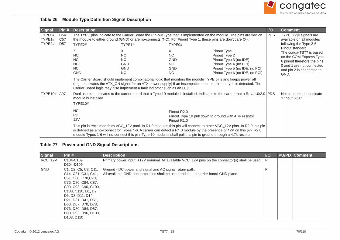
Copyright © 2012 congatec AG TS77m13 70/110
Table 26 Module Type Definition Signal Description
Signal Pin # Description I/O CommentTYPE0#TYPE1#TYPE2#
C54C57D57
The TYPE pins indicate to the Carrier Board the Pin-out Type that is implemented on the module. The pins are tied on the module to either ground (GND) or are no-connects (NC). For Pinout Type 1, these pins are don’t care (X).
PDS TYPE[0:2]# signals are available on all modules following the Type 2-6 Pinout standard.The conga-TS77 is based on the COM Express Type 6 pinout therefore the pins 0 and 1 are not connected and pin 2 is connected to GND.
TYPE2# TYPE1# TYPE0#
XNCNCNCNCGND
XNCNCGNDGNDNC
XNCGNDNCGNDNC
Pinout Type 1Pinout Type 2Pinout Type 3 (no IDE)Pinout Type 4 (no PCI)Pinout Type 5 (no IDE, no PCI)Pinout Type 6 (no IDE, no PCI)
The Carrier Board should implement combinatorial logic that monitors the module TYPE pins and keeps power off (e.g deactivates the ATX_ON signal for an ATX power supply) if an incompatible module pin-out type is detected. The Carrier Board logic may also implement a fault indicator such as an LED.
TYPE10# A97 Dual use pin. Indicates to the carrier board that a Type 10 module is installed. Indicates to the carrier that a Rev. 1.0/2.0 module is installed.
PDS Not connected to indicate “Pinout R2.0”.
TYPE10#
NCPD12V
Pinout R2.0Pinout Type 10 pull down to ground with 4.7k resistorPinout R1.0
This pin is reclaimed from VCC_12V pool. In R1.0 modules this pin will connect to other VCC_12V pins. In R2.0 this pin is defined as a no-connect for Types 1-6. A carrier can detect a R1.0 module by the presence of 12V on this pin. R2.0 module Types 1-6 will no-connect this pin. Type 10 modules shall pull this pin to ground through a 4.7k resistor.
Table 27 Power and GND Signal Descriptions
Signal Pin # Description I/O PU/PD CommentVCC_12V C104-C109
D104-D109Primary power input: +12V nominal. All available VCC_12V pins on the connector(s) shall be used. P
GND C1, C2, C5, C8, C11, C14, C21, C31, C41, C51, C60, C70,C73, C76, C80, C84, C87, C90, C93, C96, C100, C103, C110, D1, D2, D5, D8, D11, D14, D21, D31, D41, D51, D60, D67, D70, D73, D76, D80, D84, D87, D90, D93, D96, D100, D103, D110
Ground - DC power and signal and AC signal return path. All available GND connector pins shall be used and tied to carrier board GND plane.
P
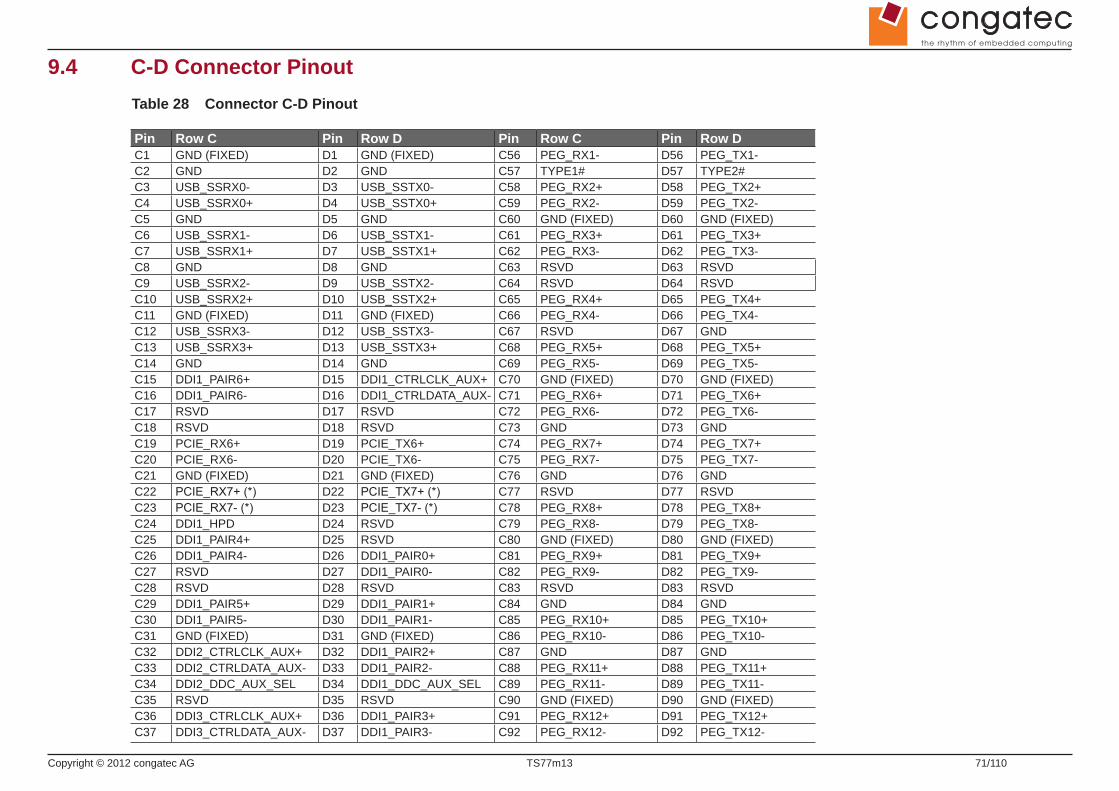
Copyright © 2012 congatec AG TS77m13 71/110
9.4 C-D Connector PinoutTable 28 Connector C-D Pinout
Pin Row C Pin Row D Pin Row C Pin Row DC1 GND (FIXED) D1 GND (FIXED) C56 PEG_RX1- D56 PEG_TX1- C2 GND D2 GND C57 TYPE1# D57 TYPE2#C3 USB_SSRX0- D3 USB_SSTX0- C58 PEG_RX2+ D58 PEG_TX2+C4 USB_SSRX0+ D4 USB_SSTX0+ C59 PEG_RX2- D59 PEG_TX2- C5 GND D5 GND C60 GND (FIXED) D60 GND (FIXED)C6 USB_SSRX1- D6 USB_SSTX1- C61 PEG_RX3+ D61 PEG_TX3+ C7 USB_SSRX1+ D7 USB_SSTX1+ C62 PEG_RX3- D62 PEG_TX3- C8 GND D8 GND C63 RSVD D63 RSVDC9 USB_SSRX2- D9 USB_SSTX2- C64 RSVD D64 RSVDC10 USB_SSRX2+ D10 USB_SSTX2+ C65 PEG_RX4+ D65 PEG_TX4+ C11 GND (FIXED) D11 GND (FIXED) C66 PEG_RX4- D66 PEG_TX4- C12 USB_SSRX3- D12 USB_SSTX3- C67 RSVD D67 GNDC13 USB_SSRX3+ D13 USB_SSTX3+ C68 PEG_RX5+ D68 PEG_TX5+ C14 GND D14 GND C69 PEG_RX5- D69 PEG_TX5- C15 DDI1_PAIR6+ D15 DDI1_CTRLCLK_AUX+ C70 GND (FIXED) D70 GND (FIXED)C16 DDI1_PAIR6- D16 DDI1_CTRLDATA_AUX- C71 PEG_RX6+ D71 PEG_TX6+ C17 RSVD D17 RSVD C72 PEG_RX6- D72 PEG_TX6- C18 RSVD D18 RSVD C73 GND D73 GNDC19 PCIE_RX6+ D19 PCIE_TX6+ C74 PEG_RX7+ D74 PEG_TX7+ C20 PCIE_RX6- D20 PCIE_TX6- C75 PEG_RX7- D75 PEG_TX7- C21 GND (FIXED) D21 GND (FIXED) C76 GND D76 GNDC22 PCIE_RX7+ (*) D22 PCIE_TX7+ (*) C77 RSVD D77 RSVDC23 PCIE_RX7- (*) D23 PCIE_TX7- (*) C78 PEG_RX8+ D78 PEG_TX8+ C24 DDI1_HPD D24 RSVD C79 PEG_RX8- D79 PEG_TX8- C25 DDI1_PAIR4+ D25 RSVD C80 GND (FIXED) D80 GND (FIXED)C26 DDI1_PAIR4- D26 DDI1_PAIR0+ C81 PEG_RX9+ D81 PEG_TX9+ C27 RSVD D27 DDI1_PAIR0- C82 PEG_RX9- D82 PEG_TX9- C28 RSVD D28 RSVD C83 RSVD D83 RSVDC29 DDI1_PAIR5+ D29 DDI1_PAIR1+ C84 GND D84 GNDC30 DDI1_PAIR5- D30 DDI1_PAIR1- C85 PEG_RX10+ D85 PEG_TX10+ C31 GND (FIXED) D31 GND (FIXED) C86 PEG_RX10- D86 PEG_TX10- C32 DDI2_CTRLCLK_AUX+ D32 DDI1_PAIR2+ C87 GND D87 GND C33 DDI2_CTRLDATA_AUX- D33 DDI1_PAIR2- C88 PEG_RX11+ D88 PEG_TX11+ C34 DDI2_DDC_AUX_SEL D34 DDI1_DDC_AUX_SEL C89 PEG_RX11- D89 PEG_TX11- C35 RSVD D35 RSVD C90 GND (FIXED) D90 GND (FIXED) C36 DDI3_CTRLCLK_AUX+ D36 DDI1_PAIR3+ C91 PEG_RX12+ D91 PEG_TX12+ C37 DDI3_CTRLDATA_AUX- D37 DDI1_PAIR3- C92 PEG_RX12- D92 PEG_TX12-
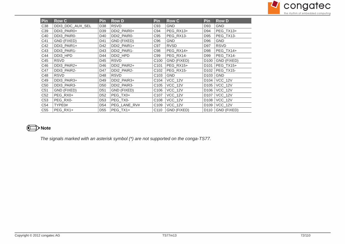
Copyright © 2012 congatec AG TS77m13 72/110
Pin Row C Pin Row D Pin Row C Pin Row DC38 DDI3_DDC_AUX_SEL D38 RSVD C93 GND D93 GND C39 DDI3_PAIR0+ D39 DDI2_PAIR0+ C94 PEG_RX13+ D94 PEG_TX13+ C40 DDI3_PAIR0- D40 DDI2_PAIR0- C95 PEG_RX13- D95 PEG_TX13- C41 GND (FIXED) D41 GND (FIXED) C96 GND D96 GND C42 DDI3_PAIR1+ D42 DDI2_PAIR1+ C97 RVSD D97 RSVDC43 DDI3_PAIR1- D43 DDI2_PAIR1- C98 PEG_RX14+ D98 PEG_TX14+ C44 DDI3_HPD D44 DDI2_HPD C99 PEG_RX14- D99 PEG_TX14- C45 RSVD D45 RSVD C100 GND (FIXED) D100 GND (FIXED) C46 DDI3_PAIR2+ D46 DDI2_PAIR2+ C101 PEG_RX15+ D101 PEG_TX15+ C47 DDI3_PAIR2- D47 DDI2_PAIR2- C102 PEG_RX15- D102 PEG_TX15- C48 RSVD D48 RSVD C103 GND D103 GND C49 DDI3_PAIR3+ D49 DDI2_PAIR3+ C104 VCC_12V D104 VCC_12V C50 DDI3_PAIR3- D50 DDI2_PAIR3- C105 VCC_12V D105 VCC_12V C51 GND (FIXED) D51 GND (FIXED) C106 VCC_12V D106 VCC_12V C52 PEG_RX0+ D52 PEG_TX0+ C107 VCC_12V D107 VCC_12V C53 PEG_RX0- D53 PEG_TX0- C108 VCC_12V D108 VCC_12V C54 TYPE0# D54 PEG_LANE_RV# C109 VCC_12V D109 VCC_12V C55 PEG_RX1+ D55 PEG_TX1+ C110 GND (FIXED) D110 GND (FIXED)
Note
The signals marked with an asterisk symbol (*) are not supported on the conga-TS77.

Copyright © 2012 congatec AG TS77m13 73/110
9.5 Boot Strap SignalsTable 29 Boot Strap Signal Descriptions
Signal Pin # Description of Boot Strap Signal I/O PU/PD CommentAC/HDA_SYNC A29 High Definition Audio Sync: This signal is a 48 kHz fixed rate sample sync to
the codec(s). It is also used to encode the stream number.O 3.3VSB PU 1K
3.3VSBAC/HDA_SYNC is a boot strap signal (see caution statement below)
AC/HDA_SDOUT A33 High Definition Audio Serial Data Out: This signal is the serial TDM data output to the codec(s). This serial output is double-pumped for a bit rate of 48 Mb/s for High Definition Audio.
O 3.3VSB PU 1K 3.3VSB
AC/HDA_SDOUT is a boot strap signal (see caution statement below)
LVDS_I2C_DAT A84 DDC lines used for flat panel detection and control. I/O 3.3V PU 2k2 3.3V
LVDS_I2C_DAT is a boot strap signal (see caution statement below).
SPKR B32 Output for audio enunciator, the “speaker” in PC-AT systems O 3.3V SPKR is a boot strap signal (see caution statement below)
PEG_LAN_RV# D54 PCI Express Graphics lane reversal input strap. Pull low on the carrier board to reverse lane order
I 3.3V PU 10k 3.3V
PEG_LANE_RV# is a boot strap signal (see caution statement below).
DDI1_CTRLDATA_AUX-SDVO1_CTRLDATADP1_AUX-HDMI_CTRLDATA
D16 Multiplexed with SDVO1_CTRLDATA, DP1_AUX- and HDMI1_CTRLDATA.DP AUX- function if DDI1_DDC_AUX_SEL is no connect.HDMI/DVI I2C CTRLDATA if DDI1_DDC_AUX_SEL is pulled high.
I/O PCIEI/O OD 3.3V
PU100k 3.3V
DDI1_CTRLDATA_AUX- is a boot strap signal (see not below).
DDI2_CTRLDATA_AUX-DP2_AUX-HDM2_CTRLDATA
C33 Multiplexed with DP2_AUX- and HDMI2_CTRLDATA.DP AUX- function if DDI2_DDC_AUX_SEL is no connect.HDMI/DVI I2C CTRLDATA if DDI2_DDC_AUX_SEL is pulled high.
I/O PCIEI/O OD 3.3V
PU100k 3.3V
DDI2_CTRLDATA_AUX- is a boot strap signal (see not below).
DDI3_CTRLDATA_AUX-DP3_AUX-HDM3_CTRLDATA
C37 Multiplexed with DP3_AUX- and HDMI3_CTRLDATA.DP AUX- function if DDI3_DDC_AUX_SEL is no connect.HDMI/DVI I2C CTRLDATA if DDI3_DDC_AUX_SEL is pulled high
I/O PCIEI/O OD 3.3V
PU100k 3.3V
DDI3_CTRLDATA_AUX- is a boot strap signal (see not below).
Caution
The signals listed in the table above are used as chipset configuration straps during system reset. In this condition (during reset), they are inputs that are pulled to the correct state by either COM Express™ internally implemented resistors or chipset internally implemented resistors that are located on the module. No external DC loads or external pull-up or pull-down resistors should change the configuration of the signals listed in the above table. External resistors may override the internal strap states and cause the COM Express™ module to malfunction and/or cause irreparable damage to the module.

Copyright © 2012 congatec AG TS77m13 74/110
10 System Resources
10.1 System Memory MapTable 30 Memory Map
Address Range (decimal) Address Range (hex) Size Description(TOM-xxxx) – TOM N.A. N.A. ACPI reclaim, PCI memory range, Video, ….1024kB – (TOM-xxxx) 100000 – N.A N.A. Extended memory869kB – 1024kB E0000 - FFFFF 128kB Runtime BIOS768kB – 896kB C0000 - DFFFF Expansion Area640kB – 768kB A0000 - BFFFF 128kB Video memory and BIOS639kB – 640kB 9FC00 - 9FFFF 1kB Extended BIOS data 0 – 639kB 00000 - 9FC00 512kB Conventional memory
Note
T.O.M. = Top of memory = max. DRAM installed
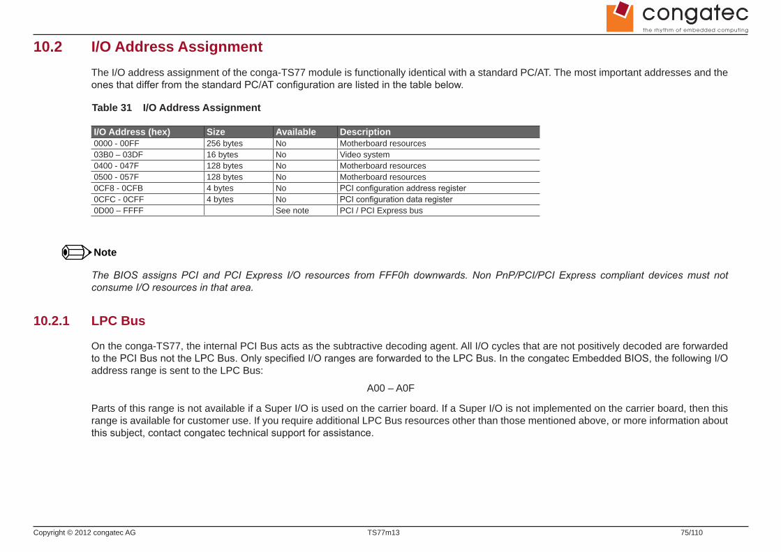
Copyright © 2012 congatec AG TS77m13 75/110
10.2 I/O Address AssignmentThe I/O address assignment of the conga-TS77 module is functionally identical with a standard PC/AT. The most important addresses and the ones that differ from the standard PC/AT configuration are listed in the table below.
Table 31 I/O Address Assignment
I/O Address (hex) Size Available Description0000 - 00FF 256 bytes No Motherboard resources03B0 – 03DF 16 bytes No Video system0400 - 047F 128 bytes No Motherboard resources0500 - 057F 128 bytes No Motherboard resources0CF8 - 0CFB 4 bytes No PCI configuration address register 0CFC - 0CFF 4 bytes No PCI configuration data register0D00 – FFFF See note PCI / PCI Express bus
Note
The BIOS assigns PCI and PCI Express I/O resources from FFF0h downwards. Non PnP/PCI/PCI Express compliant devices must not consume I/O resources in that area.
10.2.1 LPC Bus
On the conga-TS77, the internal PCI Bus acts as the subtractive decoding agent. All I/O cycles that are not positively decoded are forwarded to the PCI Bus not the LPC Bus. Only specified I/O ranges are forwarded to the LPC Bus. In the congatec Embedded BIOS, the following I/O address range is sent to the LPC Bus:
A00 – A0F
Parts of this range is not available if a Super I/O is used on the carrier board. If a Super I/O is not implemented on the carrier board, then this range is available for customer use. If you require additional LPC Bus resources other than those mentioned above, or more information about this subject, contact congatec technical support for assistance.

Copyright © 2012 congatec AG TS77m13 76/110
10.3 Interrupt Request (IRQ) LinesTable 32 IRQ Lines in PIC mode
IRQ# Available Typical Interrupt Source Connected to Pin0 No Counter 0 Not applicable1 No Keyboard Not applicable2 No Cascade Interrupt from Slave PIC Not applicable3 Yes IRQ3 via SERIRQ or PCI BUS INTx4 Yes IRQ4 via SERIRQ or PCI BUS INTx5 Yes IRQ5 via SERIRQ or PCI BUS INTx6 Yes IRQ6 via SERIRQ or PCI BUS INTx7 Yes IRQ7 via SERIRQ or PCI BUS INTx8 No Real-time Clock Not applicable9 No SCI Not applicable10 Yes IRQ10 via SERIRQ or PCI BUS INTx11 Yes IRQ11 via SERIRQ or PCI BUS INTx12 Yes IRQ12 via SERIRQ or PCI BUS INTx13 No Math processor Not applicable14 Yes PCI BUS INTx15 Yes PCI BUS INTx
Note
In PIC mode, the PCI bus interrupt lines can be routed to any free IRQ.

Copyright © 2012 congatec AG TS77m13 77/110
Table 33 IRQ Lines in APIC mode
IRQ# Available Typical Interrupt Source Connected to Pin / Function0 No Counter 0 Not applicable1 No Keyboard Not applicable2 No Cascade Interrupt from Slave PIC Not applicable3 Yes IRQ3 via SERIRQ4 Yes IRQ4 via SERIRQ5 Yes IRQ5 via SERIRQ6 Yes IRQ6 via SERIRQ7 Yes IRQ7 via SERIRQ8 No Real-time Clock Not applicable9 No SCI SCI10 Yes IRQ10 via SERIRQ11 Yes IRQ11 via SERIRQ12 Yes IRQ12 via SERIRQ13 No Math processor Not applicable14 Yes15 Yes16 No PIRQA, XHCI, Integrated VGA Controller, PCI Express Root Port 0, PCI Express Root Port 4, PEG Root Ports 0, 1, 2,
EHCI Host Controller 217 No PIRQB, PCI Express Root Port 1, PCI Express Root Port 518 No PIRQC, PCI Express Root Port 2, SMBus Controller, Thermal Controller19 No PIRQD, SATA Controller 1, SATA Controller 2, PCI Express Root Port 3, PCI Express Root Port 720 Yes PIRQE, onboard Gigabit Ethernet LAN Controller21 Yes PIRQF22 Yes PIRQG, Intel High Definition Audio Controller23 Yes PIRQH, EHCI Host Controller 1

Copyright © 2012 congatec AG TS77m13 78/110
10.4 PCI Configuration Space MapTable 34 PCI Configuration Space Map
Bus Number (hex) Device Number (hex) Function Number (hex) PCI Interrupt Routing Description00h 00h 00h N.A. Host Bridge00h 01h 00h Internal PCI Express Graphic Root Port 000h 01h 01h Internal PCI Express Graphic Root Port 100h 01h 02h Internal PCI Express Graphic Root Port 200h 02h 00h Internal VGA Graphics00h 14h 00h Internal XHCI Host Controller00h( Note1) 16h 00h Internal Management Engine (ME) Interface 100h( Note1) 16h 01h Internal Intel ME Interface 200h( Note1) 16h 02h Internal ME IDE Redirection (IDE-R) Interface00h( Note1) 16h 03h Internal ME KT (Remote Keyboard and Text)00h 19h 00h Internal Onboard Gigabit LAN Controller00h 1Ah 00h Internal EHCI Host Controller 200h 1Bh 00h Internal Intel High Definition Audio Controller00h 1Ch 00h Internal PCI Express Root Port 000h( Note2) 1Ch 01h Internal PCI Express Root Port 100h (Note2) 1Ch 02h Internal PCI Express Root Port 200h (Note2) 1Ch 03h Internal PCI Express Root Port 300h (Note2) 1Ch 04h Internal PCI Express Root Port 400h (Note2) 1Ch 05h Internal PCI Express Root Port 500h 1Ch 07h Internal PCI Express Root Port 700h 1Dh 00h Internal EHCI Host Controller 100h 1Fh 00h N.A. PCI to LPC Bridge00h 1Fh 02h Internal Serial ATA Controller 100h 1Fh 03h Internal SMBus Host Controller00h 1Fh 05h Internal Serial ATA Controller 200h 1Fh 06h Internal Thermal Subsystem01h (Note3) 00h 00h Internal PEG Port 002h (Note3) 00h 00h Internal PEG Port 103h (Note3) 00h 00h Internal PEG Port 204h (Note3) 00h 00h Internal PCI Express Port 005h (Note3) 00h 00h Internal PCI Express Port 106h (Note3) 00h 00h Internal PCI Express Port 207h (Note3) 00h 00h Internal PCI Express Port 308h (Note3) 00h 00h Internal PCI Express Port 409h (Note3) 00h 00h Internal PCI Express Port 50Ah (Note3) 00h 00h Internal PCI Express Port 6

Copyright © 2012 congatec AG TS77m13 79/110
Note
1. In the standard configuration the Intel Management Engine (ME) related devices are partly present or not present at all.
2. The PCI Express Ports are visible only if a device is attached behind them to the PCI Express Slot on the carrier board.
3. The table represents a case when a single function PCI/PCIe device is connected to all possible slots on the carrier board. The given bus numbers will change based on actual hardware configuration.
10.5 PCI Interrupt Routing MapTable 35 PCI Interrupt Routing Map
PIRQ PCI BUS INT Line ¹
APIC Mode IRQ
VGA HDA XHCI EHCI 1 EHCI 2 SM Bus + Thermal
LAN SATA1 SATA2 PEG Root Port 1
PEG Root Port 2
PEG Root Port 3
PEG Port 0
PEG Port 1
PEG Port 2
A INTA 16 x x x x x x x ² x 5 x 4
B INTB 17 x ³ x 2 x 5
C INTC 18 x x 4 x 3 x 2
D INTD 19 x x x 5 x 4 x 3
E 20 xF 21G 22 xH 23 x
PIRQ PCI-EX Root Port 0
PCI-EX Root Port 1
PCI-EX Root Port 2
PCI-EX Root Port 3
PCI-EX Root Port 4
PCI-EX Root Port 5
PCI-EX Root Port 7
PCI-EX Port 0
PCI-EX Port 1
PCI-EX Port 2
PCI-EX Port 3
PCI-EX Port 4
PCI-EX Port 5
PCI-EX Port 6 6
A x x x 2 x 5 x 4 x 3 x ² x 5 x 3
B x x x 3 x 2 x 5 x 4 x ³ x 2 x 4
C x x 4 x 3 x ² x 5 x 4 x 3 x 5
D x x x 5 x 4 x ³ x 2 x 5 x 4 x 2
EFGH

Copyright © 2012 congatec AG TS77m13 80/110
Note
1 These interrupt lines are virtual (message based).
2 Interrupt used by single function PCI Express devices (INTA).
3 Interrupt used by multifunction PCI Express devices (INTB).
4 Interrupt used by multifunction PCI Express devices (INTC).
5 Interrupt used by multifunction PCI Express devices (INTD).
6 The COM Express PCIe Port 6 is routed to the PCIe Root Port 7 of the PCH.
10.6 I²C BusThere are no onboard resources connected to the I²C bus. Address 16h is reserved for congatec Battery Management solutions.
10.7 SM BusSystem Management (SM) bus signals are connected to the Intel® BD82QM77 or BD82HM76 (QM77 or HM76) PCH and the SM bus is not intended to be used by off-board non-system management devices. For more information about this subject contact congatec technical support.

Copyright © 2012 congatec AG TS77m13 81/110
11 BIOS Setup DescriptionThe following section describes the BIOS setup program. The BIOS setup program can be used to view and change the BIOS settings for the module. Only experienced users should change the default BIOS settings.
11.1 Entering the BIOS Setup Program.The BIOS setup program can be accessed by pressing the <DEL> or <F2> key during POST.
11.1.1 Boot Selection Popup
The BIOS offers the possibility to access a Boot Selection Popup menu by pressing the <F11> key during POST. If this option is used, a selection will be displayed immediately after POST allowing the operator to select either the boot device that should be used or an option to enter the BIOS setup program.
11.2 Setup Menu and NavigationThe congatec BIOS setup screen is composed of the menu bar and two main frames. The menu bar is shown below:
Main Advanced Boot Security Save & Exit
The left frame displays all the options that can be configured in the selected menu. Grayed-out options cannot be configured. Only the blue options can be configured. When an option is selected, it is highlighted in white.
Note
Entries in the option column that are displayed in bold print indicate BIOS default values.
The right frame displays the key legend. Above the key legend is an area reserved for text messages. These text messages explain the options and the possible impacts when changing the selected option in the left frame.
The setup program uses a key-based navigation system. Most of the keys can be used at any time while in setup. The table below explains the supported keys:

Copyright © 2012 congatec AG TS77m13 82/110
Key Description← → Left/Right Select a setup menu (e.g. Main, Boot, Exit).↑ ↓ Up/Down Select a setup item or sub menu.+ - Plus/Minus Change the field value of a particular setup item.Tab Select setup fields (e.g. in date and time).F1 Display General Help screen.F2 Load previous settings.F9 Load optimal default settings.F10 Save changes and exit setup.ESC Discard changes and exit setup.ENTER Display options of a particular setup item or enter submenu.
11.3 Main Setup ScreenWhen you first enter the BIOS setup, you will enter the Main setup screen. You can always return to the Main setup screen by selecting the Main tab. The Main screen reports BIOS, processor, memory and board information and is for configuring the system date and time.
Feature Options DescriptionMain BIOS Version no option Displays the main BIOS version.OEM BIOS Version no option Displays the additional OEM BIOS version.Build Date no option Displays the date the BIOS was built.Product Revision no option Displays the hardware revision of the board.Serial Number no option Displays the serial number of the board.BC Firmware Rev. no option Displays the revision of the congatec board controller.MAC Address no option Displays the MAC address of the onboard Ethernet controller.Boot Counter no option Displays the number of boot-ups. (max. 16777215).Running Time no option Displays the time the board is running [in hours max. 65535].►Platform Information submenu Opens the platform information submenu.System Date Day of week, month/
day/yearSpecifies the current system dateNote: The date is in month/day/year format.
System Time Hour:Minute:Second Specifies the current system time.Note: The time is in 24 hour format.

Copyright © 2012 congatec AG TS77m13 83/110
11.3.1 Platform Information Submenu
The Platform Information submenu offers additional hardware and software information.
Feature Options DescriptionProcessor Type no option Displays the processor ID string. The “Processor Type” text itself is not displayed
just the ID string.Codename no option Displays the processor codenameProcessor Speed no option Displays the processor speed.Processor Signature no option Displays the processor signature.Stepping no option Displays the processor stepping.Microcode Revision no option Displays the processor microcode revision .Processor Cores no option Displays the number of processor cores.IGD VBIOS Version no option Displays the video BIOS version.IGD HW Version no option Displays the version of the graphics controller.Total Memory no option Displays the total amount of installed memory.Codename no option Displays the codename of the platform controller hub (PCH).Intel PCH SKU Name no option Displays the SKU name of the PCH.Stepping no option Displays the PCH stepping.
11.4 Advanced SetupSelect the Advanced tab from the setup menu to enter the Advanced BIOS Setup screen. The menu is used for setting advanced features and only features described within this user’s guide are listed.
Main Advanced Boot Security Save & ExitGraphics WatchdogHardware Health MonitoringPCI & PCI ExpressACPIRTC WakeTrusted ComputingCPU Chipset SATAUSBSuper IO

Copyright © 2012 congatec AG TS77m13 84/110
Main Advanced Boot Security Save & ExitSerial Port Console RedirectionUEFI Network Stack
11.4.1 Graphics Submenu
Feature Options DescriptionInternal Graphics Auto
DisabledEnabled
Auto: Disables IGD if external Graphics is detected.Disabled: IGD always disabled. Enabled: IGD always enabled.
Primary Graphics Device AutoIGDPEGPCI/PCIe
Select primary graphics adapter to be used during boot up.Auto: BIOS will select it automatically.IGD: Internal Graphics Device (IGD) located in Chipset.PEG: External PCI Express Graphics (PEG) card attached to the PEG port.PCI/PCIe: PCI/PCIe graphics card attached to some other (not PEG) PCI/PCIe port.
IGD Pre-Allocated Graphics Memory
32M, 64M, 96M, 128M, 160M, 192M, 224M, 256M, 288M, 320M, 352M, 384M, 416M, 448M, 480M, 512M, 1024M
Select amount of pre-allocated (fixed) graphics memory used by the Internal Graphics Device.
IGD Total Graphics Memory 128MB256MBMAX
Select amount of total graphics memory that maybe used by the Internal Graphics Device. Memory above the fixed graphics memory will be dynamically allocated by the graphics driver according to DVMT 5.0 specification. MAX = Use as much graphics memory as possible. Depends on total system memory installed and the operating system used (see DVMT 5.0 specification).
Primary IGD Boot Display Device
Auto CRTLFPEFPEFP2EFP3
Select the Primary IGD display device(s) used for boot up.CRT selects Analog VGA display port.LFP (Local Flat Panel) selects a LVDS panel connected to the integrated LVDS port.EFPx (External Flat Panel ) selects a HDMI/DVI or DisplayPort device connected to the Digital Display Interfaces DDI1, DDI2 and DDI3.Examples for EFPx name assignment to DDI1, DDI2, DDI3:1. If only DDI2 is enabled then the EFP name is assigned to DDI2.2. If both port DDI1 and DDI2 are enabled then EFP is assigned to DDI1 and EFP2 is assigned to DDI2.EFP selections are valid only when DDI1, DDI2 and/or DDI3 are enabled.
Secondary IGD Boot Display Device
DisabledCRTLFPEFPEFP2EFP3
Select the Secondary IGD display device(s) used for boot up.
VGA modes will be supported only on Primary display.For other details see Primary IGD Boot Display Device.
Active LFP Configuration No Local Flat PanelIntegrated LVDS
Select the active local flat panel configuration.
Always Try Auto Panel Detect NoYes
If set to ‘Yes’ the BIOS will first look for an EDID data set in an external EEPROM to configure the Local Flat Panel. Only if no external EDID data set can be found, the data set selected under ‘Local Flat Panel Type’ will be used as a fallback data set.

Copyright © 2012 congatec AG TS77m13 85/110
Feature Options DescriptionLocal Flat Panel Type Auto
VGA 640x480 1x18 (002h)VGA 640x480 1x18 (013h)WVGA 800x480 1x24 (01Bh)SVGA 800x600 1x18 (01Ah)XGA 1024x768 1x18 (006h)XGA 1024x768 2x18 (007h)XGA 1024x768 1x24 (008h)XGA 1024x768 2x24 (012h)WXGA 1280x768 1x24 (01Ch)SXGA 1280x1024 2x24 (00Ah)SXGA 1280x1024 2x24 (018h)UXGA 1600x1200 2x24 (00Ch)WUXGA 1920x1200 2x18 (015h)WUXGA 1920x1200 2x24 (00Dh)Customized EDID™ 1Customized EDID™ 2Customized EDID™ 3
Select a predefined LFP type or choose Auto to let the BIOS automatically detect and configure the attached LVDS panel. Auto detection is performed by reading an EDID data set via the video I²C bus.The number in brackets specifies the congatec internal number of the respective panel data set.Note: Customized EDID™ utilizes an OEM defined EDID™ data set stored in the BIOS flash device.
Backlight Inverter Type NonePWMI2C
Select the type of backlight inverter used.PWM = Use IGD PWM signal.I2C = Use I2C backlight inverter device connected to the video I²C bus.
PWM Inverter Polarity NormalInverted
Select PWM inverter polarity. Only visible if Backlight Inverter Type is set to PWM .
PWM Inverter Frequency (Hz) 200 - 40000 Set the PWM inverter frequency in Hz. Only visible if Backlight Inverter Type is set to PWM.Backlight Setting 0%, 10%, 25%, 40%, 50%, 60%,
75%, 90%, 100%Actual backlight value in percent of the maximum setting.
Inhibit Backlight NoPermanentUntil End Of POST
Decide whether the backlight on signal should be activated when the panel is activated or whether it should remain inhibited until the end of BIOS POST or permanently.
Invert Backlight Setting NoYes
Allow to invert backlight control values if required for the actual I2C type backlight hardware controller.
Digital Display Interface 1 (DDI1)
DisabledSDVODisplay PortHDMI/DVI
Select the output type of the digital display interface.
Select SDVO Device SDVO DVI Only SDVO DVI supported.Digital Display Interface 2 (DDI2)
DisabledDisplay PortHDMI/DVI
Select the output type of the digital display interface.
Digital Display Interface 3 (DDI3)
DisabledDisplay PortHDMI/DVI
Select the output type of the digital display interface.
Display Mode Persistence DisabledEnable
Display mode persistence means that previous display device configurations can be ‘remembered’ and restored by the system. E.g. a dual view DVI configuration will automatically be restored if both DVI monitors are connected again even if during an earlier boot only one DVI monitor had been connected and active.
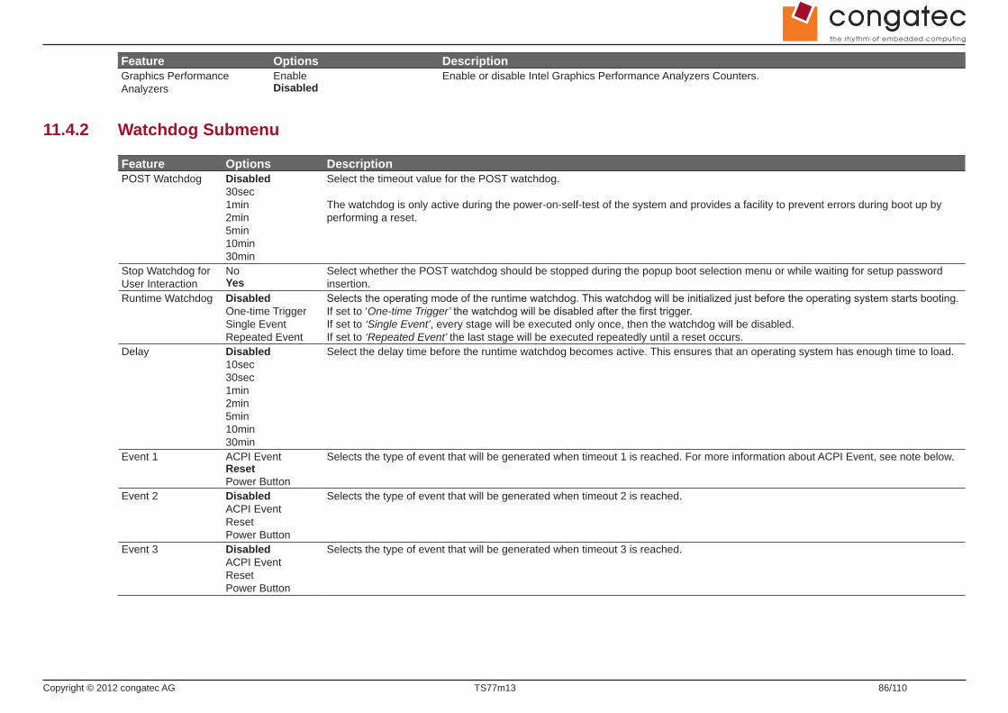
Copyright © 2012 congatec AG TS77m13 86/110
Feature Options DescriptionGraphics Performance Analyzers
EnableDisabled
Enable or disable Intel Graphics Performance Analyzers Counters.
11.4.2 Watchdog Submenu
Feature Options DescriptionPOST Watchdog Disabled
30sec1min2min5min10min30min
Select the timeout value for the POST watchdog.
The watchdog is only active during the power-on-self-test of the system and provides a facility to prevent errors during boot up by performing a reset.
Stop Watchdog for User Interaction
NoYes
Select whether the POST watchdog should be stopped during the popup boot selection menu or while waiting for setup password insertion.
Runtime Watchdog DisabledOne-time TriggerSingle EventRepeated Event
Selects the operating mode of the runtime watchdog. This watchdog will be initialized just before the operating system starts booting.If set to ‘One-time Trigger’ the watchdog will be disabled after the first trigger.If set to ‘Single Event’, every stage will be executed only once, then the watchdog will be disabled.If set to ‘Repeated Event’ the last stage will be executed repeatedly until a reset occurs.
Delay Disabled10sec30sec1min2min5min10min30min
Select the delay time before the runtime watchdog becomes active. This ensures that an operating system has enough time to load.
Event 1 ACPI EventResetPower Button
Selects the type of event that will be generated when timeout 1 is reached. For more information about ACPI Event, see note below.
Event 2 DisabledACPI EventResetPower Button
Selects the type of event that will be generated when timeout 2 is reached.
Event 3 DisabledACPI EventResetPower Button
Selects the type of event that will be generated when timeout 3 is reached.

Copyright © 2012 congatec AG TS77m13 87/110
Feature Options DescriptionTimeout 1 1sec
2sec5sec10sec30sec1min2min5min10min30min
Selects the timeout value for the first stage watchdog event.
Timeout 2 see above Selects the timeout value for the second stage watchdog event.Timeout 3 see above Selects the timeout value for the third stage watchdog event.Watchdog ACPI Event
ShutdownRestart
Select the operating system event that is initiated by the watchdog ACPI event. These options perform a critical but orderly operating system shutdown or restart.
Note
In ACPI mode it is not possible for a “Watchdog ACPI Event” handler to directly restart or shutdown the OS. For this reason, the congatec BIOS will do one of the following:
For Shutdown: An over temperature notification is executed. This causes the OS to shut down in an orderly fashion.
For Restart: An ACPI fatal error is reported to the OS.
Additionally, the conga-TS77 module does not support the watchdog NMI mode. COM Express type 6 modules do not support the PCI bus and therefore the PCI_SERR# signal is not available. There is no way to drive a NMI to the processor without the presence of the PCI_SERR# PCI bus signal.

Copyright © 2012 congatec AG TS77m13 88/110
11.4.3 Hardware Health Monitoring Submenu
Feature Options DescriptionCPU Temperature no option Displays the actual CPU Temperature in °C.Board Temperature 1 no option Displays the actual Board Temperature 1 in °C.Board Temperature 2 no option Displays the actual Board Temperature 2 in °C.Board Temperature 3 no option Displays the actual Board Temperature 3 in °C.12V Standard no option Displays the actual voltage of the 12V Standard power supply.5V Standby no option Displays the actual voltage of the 5V Standby power supply.CPU Fan Speed no option Displays the actual CPU Fan Speed in RPM.Fan PWM Frequency Mode Low Frequency
High FrequencySelect fan PWM base frequency mode.Low frequency: 35.3HzHigh frequency: 22.5kHz
Continuous Tacho Reading DisabledEnabled
If enabled, the fan tacho pulses are measured continuously instead of once per second. Helps to avoid audible ‘pulsing’ of the fan as the speed would be set to 100% for a very short time during measurement.
Pulses Per Revolution 1, 2, 3, 4 Select number of pulses per revolution generated by the attached fan.Automatic Fan Speed Control Disabled
EnabledEnable hardware fan speed control. Independent from any operating system the fan will be turned on once a certain start temperature is reached and linearly ramped up to the defined maximum speed within the given temperature range.
Fan Control Temperature CPU TemperatureBoard Temperature 1Board Temperature 2Board Temperature 3
Select which temperature input is used for the automatic fan speed control.
Start Temperature 30, 40, 50, 60, 70, 80, 90, 100°C
At this temperature the fan will be turned on at the defined minimum fan speed.
Temperature Range 5, 10, 15, 20, 25, 30, 40, 55, 80°C
Within this temperature range the fan will ramp up to the defined maximum fan speed.
Minimum Fan Speed Fan Off, 10%, 15%, 20%, 25%, 30%, 35%, 40%, 45%, 50%, 55%, 60%, 65%, 70%, 75%, 80%, 85%, 90%, 95% 100%
Select minimum/start fan speed to be set when the start temperature of the control slope is reached.
Maximum Fan Speed Fan Off, 10%, 15%, 20%, 25%, 30%, 35%, 40%, 45%, 50%, 55%, 60%, 65%, 70%, 75%, 80%, 85%, 90%, 95% 100%
Select maximum/end fan speed to be ramped up to until the end temperature of the control slope is reached.
Fan Always On At Minimum Speed
DisabledEnabled
If enabled, the fan will always run at least at the selected minimum speed, even if the control temperature is below the fan control start temperature. This is to ensure a minimum air flow all the time.
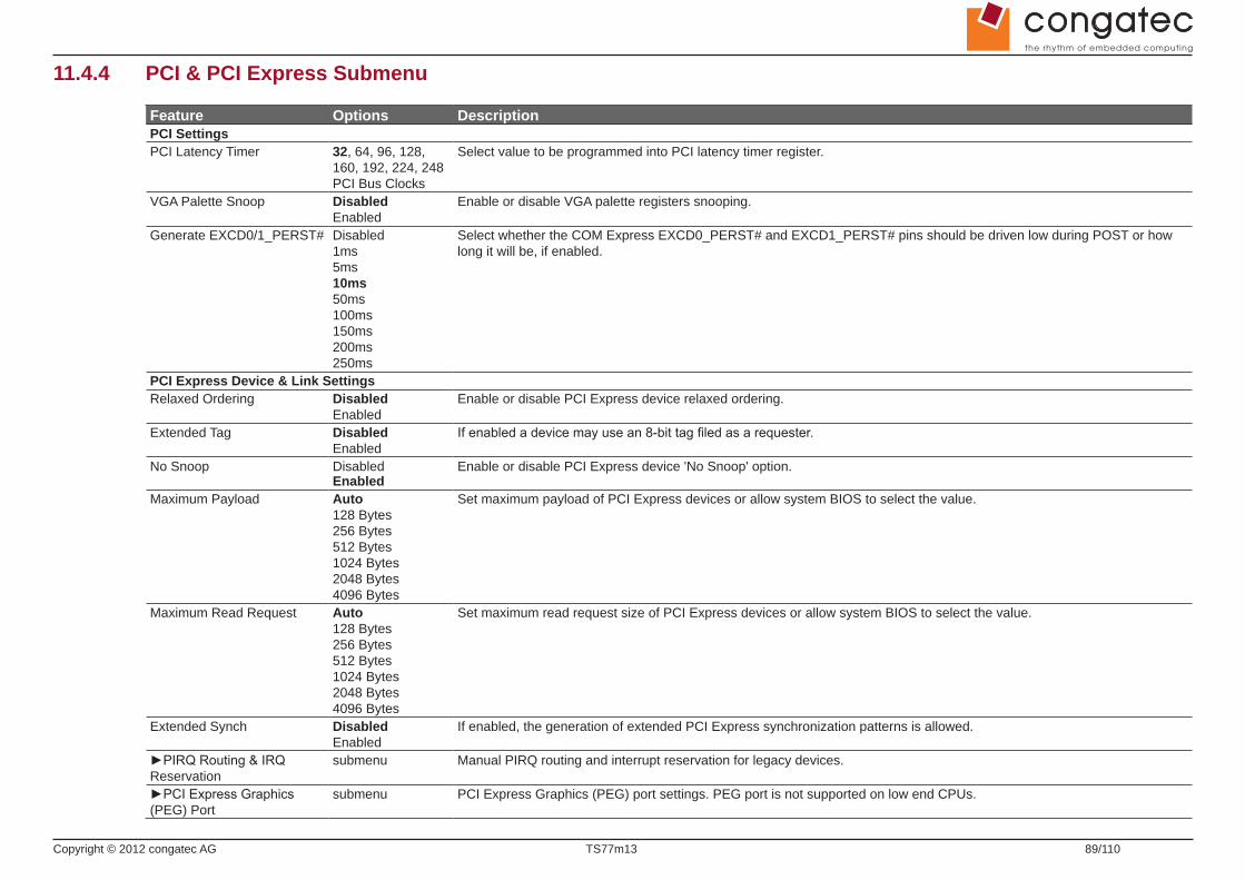
Copyright © 2012 congatec AG TS77m13 89/110
11.4.4 PCI & PCI Express Submenu
Feature Options DescriptionPCI SettingsPCI Latency Timer 32, 64, 96, 128,
160, 192, 224, 248 PCI Bus Clocks
Select value to be programmed into PCI latency timer register.
VGA Palette Snoop DisabledEnabled
Enable or disable VGA palette registers snooping.
Generate EXCD0/1_PERST# Disabled1ms5ms10ms50ms100ms150ms200ms250ms
Select whether the COM Express EXCD0_PERST# and EXCD1_PERST# pins should be driven low during POST or how long it will be, if enabled.
PCI Express Device & Link SettingsRelaxed Ordering Disabled
EnabledEnable or disable PCI Express device relaxed ordering.
Extended Tag Disabled Enabled
If enabled a device may use an 8-bit tag filed as a requester.
No Snoop Disabled Enabled
Enable or disable PCI Express device 'No Snoop' option.
Maximum Payload Auto128 Bytes256 Bytes512 Bytes1024 Bytes2048 Bytes4096 Bytes
Set maximum payload of PCI Express devices or allow system BIOS to select the value.
Maximum Read Request Auto128 Bytes256 Bytes512 Bytes1024 Bytes2048 Bytes4096 Bytes
Set maximum read request size of PCI Express devices or allow system BIOS to select the value.
Extended Synch DisabledEnabled
If enabled, the generation of extended PCI Express synchronization patterns is allowed.
►PIRQ Routing & IRQ Reservation
submenu Manual PIRQ routing and interrupt reservation for legacy devices.
►PCI Express Graphics (PEG) Port
submenu PCI Express Graphics (PEG) port settings. PEG port is not supported on low end CPUs.

Copyright © 2012 congatec AG TS77m13 90/110
Feature Options Description►PCI Express Port 0 submenu Opens the PCI Express Port submenu►PCI Express Port 1 submenu Opens the PCI Express Port submenu►PCI Express Port 2 submenu Opens the PCI Express Port submenu►PCI Express Port 3 submenu Opens the PCI Express Port submenu►PCI Express Port 4 submenu Opens the PCI Express Port submenu►PCI Express Port 5 submenu Opens the PCI Express Port submenu►PCI Express Port 6 submenu Opens the PCI Express Port submenu
11.4.4.1 PIRQ Routing & IRQ Reservation Submenu
Feature Options DescriptionPIRQA Auto, IRQ3, IRQ4,
IRQ5, IRQ6, IRQ10, IRQ11, IRQ14, IRQ15
Set interrupt for selected PIRQ. Please refer to the board’s resource list for a detailed list of devices connected to the respective PIRQ.NOTE: These settings will only be effective while operating in PIC (non-IOAPIC) interrupt mode.
PIRQB same as PIRQA same as PIRQAPIRQC same as PIRQA same as PIRQAPIRQD same as PIRQA same as PIRQAPIRQE same as PIRQA same as PIRQAPIRQF same as PIRQA same as PIRQAPIRQG same as PIRQA same as PIRQAPIRQH same as PIRQA same as PIRQAReserve Legacy Interrupt 1 None, IRQ3,
IRQ4, IRQ5, IRQ6, IRQ10, IRQ11, IRQ14, IRQ15
The interrupt reserved here will not be assigned to any PCI or PCI Express device and thus maybe available for some legacy bus device.
Reserve Legacy Interrupt 2 same as Reserve Legacy Interrupt 1
same as Reserve Legacy Interrupt 1

Copyright © 2012 congatec AG TS77m13 91/110
11.4.4.2 PCI Express Graphics (PEG) Port Submenu
Feature Options DescriptionPCI Express Graphics (PEG) Port
Disabled EnabledAuto
Disabled = Disable internal PEG interface devices and do not detect the devices connected to PEG port.Enabled = Enable internal PEG interface devices also if no device is detected on PEG port.Auto = Disable internal PEG interface devices if no device is detected on PEG port.
PEG Port Configuration 1x162x81x8+2x4
It determines how many ports, with certain widths, will be formed from available 16 PCIe lanes.
PEG0 no option Displays the width and the operation mode at which the attached device currently operates on PEG0 port (B0:D1:F0).Some Gen3, Gen2 devices start up in Gen1 mode and their OS driver just sets them to Gen3 or Gen2 mode.
PEG0 Speed AutoGen1Gen2Gen3
PEG0 port (B0:D1:F0) max. speed Auto = Gen1, Gen2 or Gen3 Gen1 = 2.5GT/s Gen2 = 5.0GT/s Gen3 = 8.0GT/s Some older non-compliant PCI Express devices will function just if Gen1 is selected.
PEG0 ASPM Disabled AutoASPM L0sASPM L1ASPM L0sL1
Control ASPM support for the PEG device. This has no effect if PEG is not the currently active device.
ASPM L0s DisabledRoot Port OnlyEndpoint Port OnlyBoth Root and Endpoint Ports
Enable PCIe ASPM L0s on PEG0 port (B0:D1:F0).
PEG1 no option Displays the width and the operation mode at which the attached device currently operates on PEG1 port (B0:D1:F1).Some Gen3, Gen2 devices start up in Gen1 mode and their OS driver just sets them to Gen3 or Gen2 mode.
PEG1 Speed AutoGen1Gen2Gen3
PEG1 port (B0:D1:F1) max. speed Auto = Gen1, Gen2 or Gen3 Gen1 = 2.5GT/s Gen2 = 5.0GT/s Gen3 = 8.0GT/s Some older non-compliant PCI Express devices will function just if Gen1 is selected.
PEG1 ASPM Disabled AutoASPM L0sASPM L1ASPM L0sL1
Control ASPM support for the PEG device. This has no effect if PEG is not the currently active device.
ASPM L0s DisabledRoot Port OnlyEndpoint Port OnlyBoth Root and Endpoint Ports
Enable PCIe ASPM L0s on PEG1 port (B0:D1:F1).

Copyright © 2012 congatec AG TS77m13 92/110
Feature Options DescriptionPEG2 no option Displays the width and the operation mode at which the attached device currently operates on PEG2 port (B0:D1:F2).
Some Gen3, Gen2 devices start up in Gen1 mode and their OS driver just sets them to Gen3 or Gen2 mode.PEG2 Speed Auto
Gen1Gen2Gen3
PEG2 port (B0:D1:F2) max. speed Auto = Gen1, Gen2 or Gen3 Gen1 = 2.5GT/s Gen2 = 5.0GT/s Gen3 = 8.0GT/s Some older non-compliant PCI Express devices will function just if Gen1 is selected.
PEG2 ASPM Disabled AutoASPM L0sASPM L1ASPM L0sL1
Control ASPM support for the PEG device. This has no effect if PEG is not the currently active device.
ASPM L0s DisabledRoot Port OnlyEndpoint Port OnlyBoth Root and Endpoint Ports
Enable PCIe ASPM L0s on PEG2 port (B0:D1:F2).
Detect Non-compliant Device DisabledEnabled
Try to detect also a non-compliant PCI Express Device on the PEG port.
De-emphasis Control -6 dB-3.5 dB
Configure the De-emphasis control on the PEG.
Note
PEG1 port related items will be displayed only when 2x8 or 1x8+2x4 option is selected as PEG Port Configuration.
PEG2 port related items will be displayed only when 1x8+2x4 option is selected as PEG Port Configuration.
11.4.4.3 PCI Express Port Submenu
Feature Options DescriptionPCI Express Port x Disabled
EnabledEnable or disable the respective PCI Express port x.
ASPM DisabledL0sL1L0sL1Auto
PCI Express Active State Power Management settings.
PME SCI Disabled Enabled
Enable or disable PCI Express PME (power management event) SCI.
Always Enable Port Disabled Enabled
Disabled = Disable the internal PCI Express interface device if no device is detected on the port.Enabled = Enable the internal PCI Express interface device also if no device is detected on the port.

Copyright © 2012 congatec AG TS77m13 93/110
Feature Options DescriptionPCIe Speed Auto
Gen1Maximum speed of the PCIe port.Auto = Gen1 or Gen2Gen1 = 2.5GT/sSome older non-compliant PCI Express devices will function just if Gen1 is selected. Some Gen2 devices start up in Gen1 mode and just their OS driver sets them to Gen2 mode.
11.4.5 ACPI Submenu
Feature Options DescriptionHibernation Support Disabled
EnabledEnable or disable system ability to hibernate (operating system S4 sleep state). This option may not be effective with some operating systems.
ACPI Sleep State Suspend Disabled S3 (Suspend to RAM)
Select the state used for ACPI system sleep/suspend.
S3 Video Repost DisabledEnabled
Enable or disable video BIOS re-post on S3 resume. Required by some operating systems.
Critical Trip Point 71, 79, 87, 95, 103, 111, 119, 127°C
Specifies the temperature threshold at which the ACPI aware OS performs a critical shutdown.
Native PCI Express Support DisabledEnabled
Enable or disable native OS PCI Express support.
Native ASPM Support DisabledEnabled
If enabled, the OS will control the ASPM support for the PCI Express devices. If disabled, the BIOS will control the ASPM support for the PCI Express devices.
Power Supply ATXAT / 12V only
Select ATX or AT power supply type.Set to AT in case you want Windows to display the “It is safe to turn the computer off” message after shutdown .
Lid Button Support DisabledEnabled
Configure COM Express LID# Signal to act as ACPI lid button.
Sleep Button Support DisabledEnabled
Configure COM Express SLEEP# signal to act as ACPI sleep button.
11.4.6 RTC Wake Submenu
Feature Options DescriptionWake System At Fixed Time Disabled
EnabledEnable system to wake from S5 using RTC alarm.
Wake up hour Specify wake up hour.Wake up minute Specify wake up minute.Wake up second Specify wake up second.

Copyright © 2012 congatec AG TS77m13 94/110
11.4.7 Trusted Computing Submenu
Feature Options DescriptionSecurity Device Support Disabled
EnabledEnable or disable TPM support. System reset is required after change.
User Confirmation DisabledEnabled
Enable or disable user confirmation requests for certain transactions.
TPM State DisabledEnabled
Enable or disable TPM chip.Note: System might restart several times during POST to acquire target state.
Pending Operation None,Enable Take Ownership,Disable Take Ownership,TPM Clear
Perform selected TPM chip operation.Note: System might restart several times during POST to perform selected operation.
11.4.8 CPU Submenu
Feature Options DescriptionActive Processor Cores All
123
Set number of cores to be enabled.
Hyper-Threading DisabledEnabled
Enable or disable Hyper-Threading support.
Execute Disable Bit DisabledEnabled
Enable or disable the Execute Disable Bit (XD) of the processor. With the XD bit set to enabled certain classes of malicious buffer overflow attacks can be prevented when combined with a supporting OS.
Limit CPUID Maximum DisabledEnabled
When enabled, the processor will limit the maximum CPUID input value to 03h when queried, even if the processor supports a higher CPUID input value. When disabled, the processor will return the actual maximum CPUID input value of the processor when queried. Limiting the CPUID input value may be required for older operating systems that cannot handle the extra CPUID information returned when using the full CPUID input value.
Hardware Prefetcher DisabledEnabled
Enable or disable the Mid Level Cache (MLC) streamer prefetcher.
Adjacent Cache Line Prefetch DisabledEnabled
Enable or disable prefetching of adjacent cache lines.
Intel Virtualization Technology DisabledEnabled
Enable or disable support for the Intel virtualization technology.
Power ManagementIntel(R) SpeedStep(tm) Disabled
EnabledDisabled: CPU speed is set to maximum and cannot be altered by the operating system.Enabled: CPU speed is controlled by the operating system.
CPU Turbo Mode DisabledEnabled
Disabled: CPU speed cannot be altered by the intel software driver above the CPU nominal operating frequency. Enabled: CPU speed can be altered by the Intel software driver above the CPU nominal operating frequency.
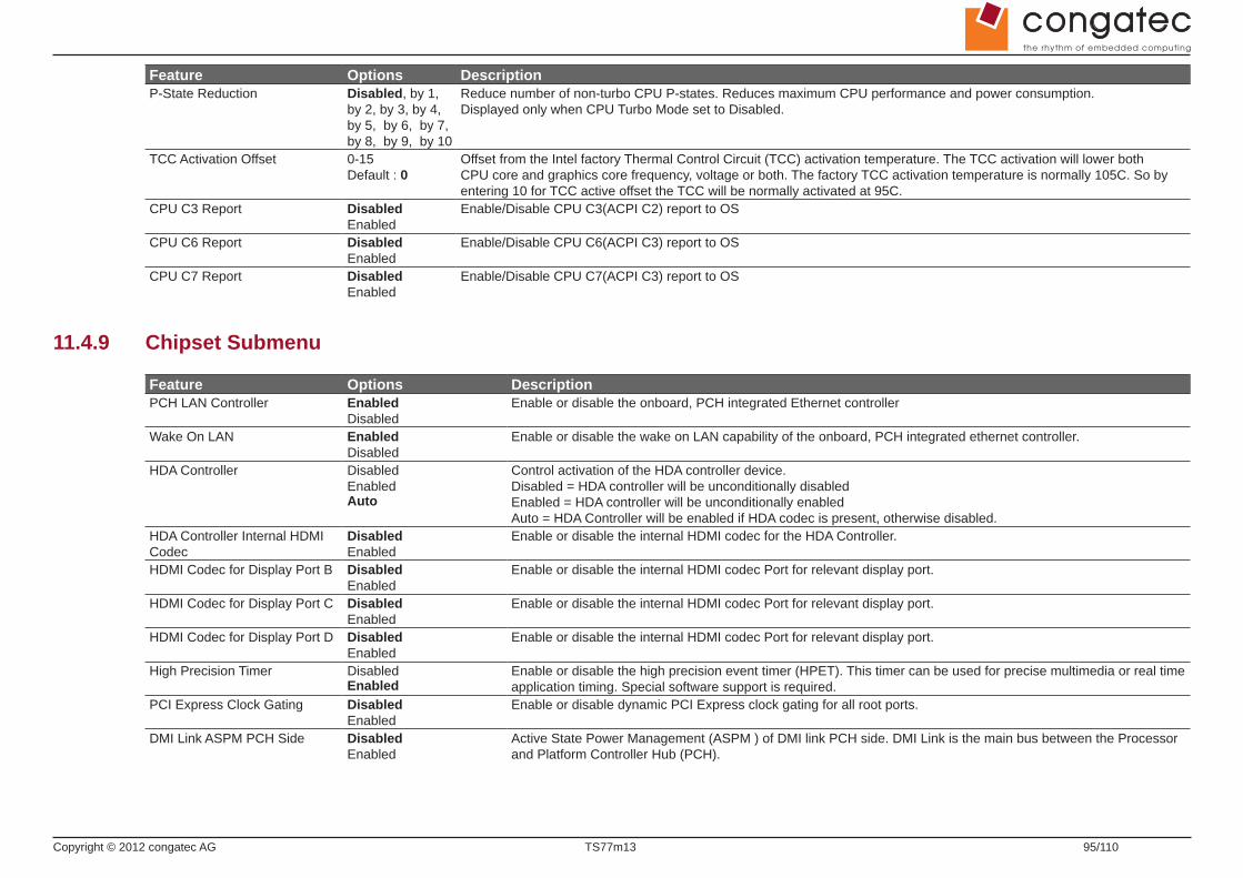
Copyright © 2012 congatec AG TS77m13 95/110
Feature Options DescriptionP-State Reduction Disabled, by 1,
by 2, by 3, by 4, by 5, by 6, by 7, by 8, by 9, by 10
Reduce number of non-turbo CPU P-states. Reduces maximum CPU performance and power consumption.Displayed only when CPU Turbo Mode set to Disabled.
TCC Activation Offset 0-15Default : 0
Offset from the Intel factory Thermal Control Circuit (TCC) activation temperature. The TCC activation will lower both CPU core and graphics core frequency, voltage or both. The factory TCC activation temperature is normally 105C. So by entering 10 for TCC active offset the TCC will be normally activated at 95C.
CPU C3 Report DisabledEnabled
Enable/Disable CPU C3(ACPI C2) report to OS
CPU C6 Report DisabledEnabled
Enable/Disable CPU C6(ACPI C3) report to OS
CPU C7 Report DisabledEnabled
Enable/Disable CPU C7(ACPI C3) report to OS
11.4.9 Chipset Submenu
Feature Options DescriptionPCH LAN Controller Enabled
DisabledEnable or disable the onboard, PCH integrated Ethernet controller
Wake On LAN EnabledDisabled
Enable or disable the wake on LAN capability of the onboard, PCH integrated ethernet controller.
HDA Controller DisabledEnabledAuto
Control activation of the HDA controller device. Disabled = HDA controller will be unconditionally disabledEnabled = HDA controller will be unconditionally enabledAuto = HDA Controller will be enabled if HDA codec is present, otherwise disabled.
HDA Controller Internal HDMI Codec
DisabledEnabled
Enable or disable the internal HDMI codec for the HDA Controller.
HDMI Codec for Display Port B DisabledEnabled
Enable or disable the internal HDMI codec Port for relevant display port.
HDMI Codec for Display Port C DisabledEnabled
Enable or disable the internal HDMI codec Port for relevant display port.
HDMI Codec for Display Port D DisabledEnabled
Enable or disable the internal HDMI codec Port for relevant display port.
High Precision Timer DisabledEnabled
Enable or disable the high precision event timer (HPET). This timer can be used for precise multimedia or real time application timing. Special software support is required.
PCI Express Clock Gating DisabledEnabled
Enable or disable dynamic PCI Express clock gating for all root ports.
DMI Link ASPM PCH Side DisabledEnabled
Active State Power Management (ASPM ) of DMI link PCH side. DMI Link is the main bus between the Processor and Platform Controller Hub (PCH).
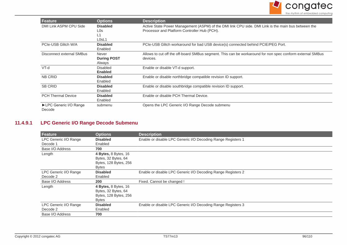
Copyright © 2012 congatec AG TS77m13 96/110
Feature Options DescriptionDMI Link ASPM CPU Side Disabled
L0sL1L0sL1
Active State Power Management (ASPM) of the DMI link CPU side. DMI Link is the main bus between the Processor and Platform Controller Hub (PCH).
PCIe-USB Glitch W/A DisabledEnabled
PCIe-USB Glitch workaround for bad USB device(s) connected behind PCIE/PEG Port.
Disconnect external SMBus NeverDuring POSTAlways
Allows to cut off the off-board SMBus segment. This can be workaround for non spec conform external SMBus devices.
VT-d DisabledEnabled
Enable or disable VT-d support.
NB CRID DisabledEnabled
Enable or disable northbridge compatible revision ID support.
SB CRID DisabledEnabled
Enable or disable southbridge compatible revision ID support.
PCH Thermal Device DisabledEnabled
Enable or disable PCH Thermal Device.
►LPC Generic I/O Range Decode
submenu Opens the LPC Generic I/O Range Decode submenu
11.4.9.1 LPC Generic I/O Range Decode Submenu
Feature Options DescriptionLPC Generic I/O Range Decode 1
DisabledEnabled
Enable or disable LPC Generic I/O Decoding Range Registers 1
Base I/O Address 700Length 4 Bytes, 8 Bytes, 16
Bytes, 32 Bytes, 64 Bytes, 128 Bytes, 256 Bytes
LPC Generic I/O Range Decode 2
DisabledEnabled
Enable or disable LPC Generic I/O Decoding Range Registers 2
Base I/O Address 200 Fixed. Cannot be changed !Length 4 Bytes, 8 Bytes, 16
Bytes, 32 Bytes, 64 Bytes, 128 Bytes, 256 Bytes
LPC Generic I/O Range Decode 2
DisabledEnabled
Enable or disable LPC Generic I/O Decoding Range Registers 3
Base I/O Address 700

Copyright © 2012 congatec AG TS77m13 97/110
Feature Options DescriptionLength 4 Bytes, 8 Bytes, 16
Bytes, 32 Bytes, 64 Bytes, 128 Bytes, 256 Bytes
LPC Generic I/O Range Decode 4
DisabledEnabled
Enable or disable LPC Generic I/O Decoding Range Registers 4
Base I/O Address 700Length 4 Bytes, 8 Bytes, 16
Bytes, 32 Bytes, 64 Bytes, 128 Bytes, 256 Bytes
Reserve Above I/O Resource in ACPI
DisabledEnabled
COM Port A Decoding DisabledEnabled
Enable or disable an LPC bus COM port range decoding.
I/O Base Address 3F8h, 2F8h, 220h, 228h, 238h, 2E8h, 338h, 3E8h
Reserve Legacy Interupt for COM
None, IRQ3, IRQ4, IRQ5, IRQ6, IRQ10, IRQ11, IRQ14,IRQ15
The interrupt reserved here will not be assigned to any PCI or PCI Express device and thus may be available for some legacy bus device.
COM Port B Decoding DisabledEnabled
Enable or disable an LPC bus COM port range decoding.
I/O Base Address 3F8h, 2F8h, 220h, 228h, 238h, 2E8h, 338h, 3E8h
Reserve Legacy Interupt for COM
None, IRQ3, IRQ4, IRQ5, IRQ6, IRQ10, IRQ11, IRQ14,IRQ15
The interrupt reserved here will not be assigned to any PCI or PCI Express device and thus may be available for some legacy bus device.
11.4.10 SATA Submenu
Feature Options DescriptionSATA Controller(s) Enabled
DisabledEnable or disable the onboard SATA controllers.
SATA Mode Selection Native IDEAHCIRAID
Select SATA controller mode.RAID option is not supported on all chipsets.
SATA Test Mode EnabledDisabled
Should be set to Disabled. Test Mode is used just for verification measurements.
Aggressive LPM Support EnabledDisabled
Enable PCH to aggressively enter link power state.
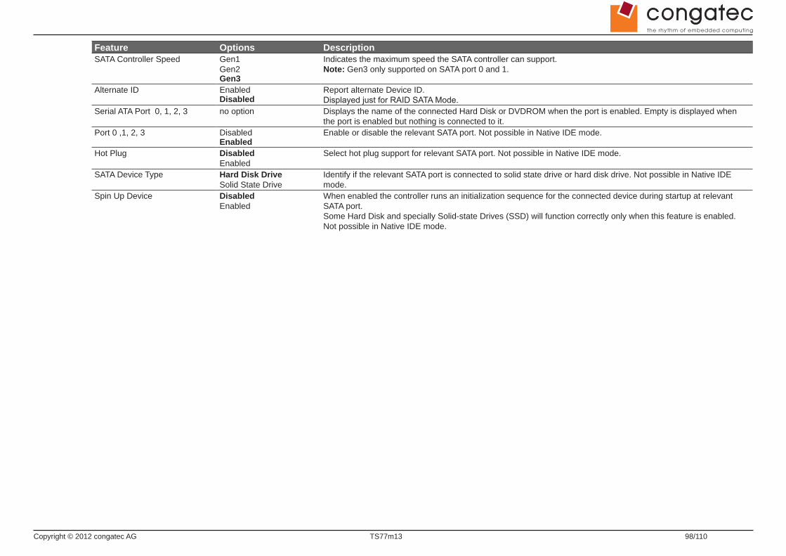
Copyright © 2012 congatec AG TS77m13 98/110
Feature Options DescriptionSATA Controller Speed Gen1
Gen2Gen3
Indicates the maximum speed the SATA controller can support.Note: Gen3 only supported on SATA port 0 and 1.
Alternate ID EnabledDisabled
Report alternate Device ID.Displayed just for RAID SATA Mode.
Serial ATA Port 0, 1, 2, 3 no option Displays the name of the connected Hard Disk or DVDROM when the port is enabled. Empty is displayed when the port is enabled but nothing is connected to it.
Port 0 ,1, 2, 3 DisabledEnabled
Enable or disable the relevant SATA port. Not possible in Native IDE mode.
Hot Plug DisabledEnabled
Select hot plug support for relevant SATA port. Not possible in Native IDE mode.
SATA Device Type Hard Disk DriveSolid State Drive
Identify if the relevant SATA port is connected to solid state drive or hard disk drive. Not possible in Native IDE mode.
Spin Up Device DisabledEnabled
When enabled the controller runs an initialization sequence for the connected device during startup at relevant SATA port.Some Hard Disk and specially Solid-state Drives (SSD) will function correctly only when this feature is enabled.Not possible in Native IDE mode.
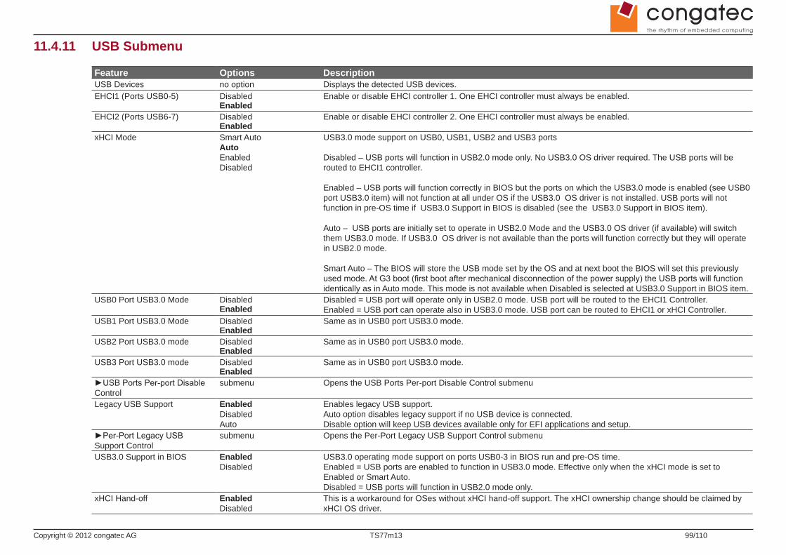
Copyright © 2012 congatec AG TS77m13 99/110
11.4.11 USB Submenu
Feature Options DescriptionUSB Devices no option Displays the detected USB devices.EHCI1 (Ports USB0-5) Disabled
EnabledEnable or disable EHCI controller 1. One EHCI controller must always be enabled.
EHCI2 (Ports USB6-7) DisabledEnabled
Enable or disable EHCI controller 2. One EHCI controller must always be enabled.
xHCI Mode Smart Auto AutoEnabledDisabled
USB3.0 mode support on USB0, USB1, USB2 and USB3 ports
Disabled – USB ports will function in USB2.0 mode only. No USB3.0 OS driver required. The USB ports will be routed to EHCI1 controller.
Enabled – USB ports will function correctly in BIOS but the ports on which the USB3.0 mode is enabled (see USB0 port USB3.0 item) will not function at all under OS if the USB3.0 OS driver is not installed. USB ports will not function in pre-OS time if USB3.0 Support in BIOS is disabled (see the USB3.0 Support in BIOS item).
Auto – USB ports are initially set to operate in USB2.0 Mode and the USB3.0 OS driver (if available) will switch them USB3.0 mode. If USB3.0 OS driver is not available than the ports will function correctly but they will operate in USB2.0 mode.
Smart Auto – The BIOS will store the USB mode set by the OS and at next boot the BIOS will set this previously used mode. At G3 boot (first boot after mechanical disconnection of the power supply) the USB ports will function identically as in Auto mode. This mode is not available when Disabled is selected at USB3.0 Support in BIOS item.
USB0 Port USB3.0 Mode DisabledEnabled
Disabled = USB port will operate only in USB2.0 mode. USB port will be routed to the EHCI1 Controller.Enabled = USB port can operate also in USB3.0 mode. USB port can be routed to EHCI1 or xHCI Controller.
USB1 Port USB3.0 Mode DisabledEnabled
Same as in USB0 port USB3.0 mode.
USB2 Port USB3.0 mode DisabledEnabled
Same as in USB0 port USB3.0 mode.
USB3 Port USB3.0 mode DisabledEnabled
Same as in USB0 port USB3.0 mode.
►USB Ports Per-port Disable Control
submenu Opens the USB Ports Per-port Disable Control submenu
Legacy USB Support EnabledDisabledAuto
Enables legacy USB support. Auto option disables legacy support if no USB device is connected. Disable option will keep USB devices available only for EFI applications and setup.
►Per-Port Legacy USB Support Control
submenu Opens the Per-Port Legacy USB Support Control submenu
USB3.0 Support in BIOS EnabledDisabled
USB3.0 operating mode support on ports USB0-3 in BIOS run and pre-OS time.Enabled = USB ports are enabled to function in USB3.0 mode. Effective only when the xHCI mode is set to Enabled or Smart Auto.Disabled = USB ports will function in USB2.0 mode only.
xHCI Hand-off EnabledDisabled
This is a workaround for OSes without xHCI hand-off support. The xHCI ownership change should be claimed by xHCI OS driver.
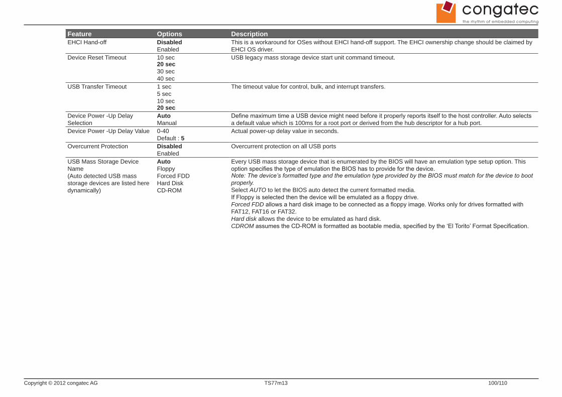
Copyright © 2012 congatec AG TS77m13 100/110
Feature Options DescriptionEHCI Hand-off Disabled
EnabledThis is a workaround for OSes without EHCI hand-off support. The EHCI ownership change should be claimed by EHCI OS driver.
Device Reset Timeout 10 sec20 sec30 sec40 sec
USB legacy mass storage device start unit command timeout.
USB Transfer Timeout 1 sec5 sec10 sec20 sec
The timeout value for control, bulk, and interrupt transfers.
Device Power -Up Delay Selection
Auto Manual
Define maximum time a USB device might need before it properly reports itself to the host controller. Auto selects a default value which is 100ms for a root port or derived from the hub descriptor for a hub port.
Device Power -Up Delay Value 0-40Default : 5
Actual power-up delay value in seconds.
Overcurrent Protection DisabledEnabled
Overcurrent protection on all USB ports
USB Mass Storage Device Name(Auto detected USB mass storage devices are listed here dynamically)
AutoFloppyForced FDDHard DiskCD-ROM
Every USB mass storage device that is enumerated by the BIOS will have an emulation type setup option. This option specifies the type of emulation the BIOS has to provide for the device.Note: The device’s formatted type and the emulation type provided by the BIOS must match for the device to boot properly.Select AUTO to let the BIOS auto detect the current formatted media.If Floppy is selected then the device will be emulated as a floppy drive.Forced FDD allows a hard disk image to be connected as a floppy image. Works only for drives formatted with FAT12, FAT16 or FAT32. Hard disk allows the device to be emulated as hard disk.CDROM assumes the CD-ROM is formatted as bootable media, specified by the ‘El Torito’ Format Specification.

Copyright © 2012 congatec AG TS77m13 101/110
11.4.11.1 USB Ports Per-port Disable Control Submenu
Feature Options DescriptionUSB0 Port Disabled Yes
NoYes = USB port is permanently disabled.No = USB port is not permanently disabled and its operation is determined with other setting in USB Configuration menu.
USB1 Port Disabled YesNo
Same as USB0 Port Disabled
USB2 Port Disabled YesNo
Same as USB0 Port Disabled
USB3 Port Disabled YesNo
Same as USB0 Port Disabled
USB4 Port Disabled YesNo
Same as USB0 Port Disabled
USB5 Port Disabled YesNo
Same as USB0 Port Disabled
USB6 Port Disabled YesNo
Same as USB0 Port Disabled
USB7 Port Disabled YesNo
Same as USB0 Port Disabled
11.4.11.2 Per-Port Legacy USB Support Control Submenu
Feature Options DescriptionUSB0 Port Legacy Support Disabled
EnabledEnable or disable legacy USB support for this port. Enabled is only effective if the port is not disabled with other setting in USB Configuration menu.
USB1 Port Legacy Support DisabledEnabled
Same as USB0 Port Legacy Support
USB2 Port Legacy Support DisabledEnabled
Same as USB0 Port Legacy Support
USB3 Port Legacy Support DisabledEnabled
Same as USB0 Port Legacy Support
USB4 Port Legacy Support DisabledEnabled
Same as USB0 Port Legacy Support
USB5 Port Legacy Support DisabledEnabled
Same as USB0 Port Legacy Support
USB6 Port Legacy Support DisabledEnabled
Same as USB0 Port Legacy Support
USB7 Port Legacy Support DisabledEnabled
Same as USB0 Port Legacy Support
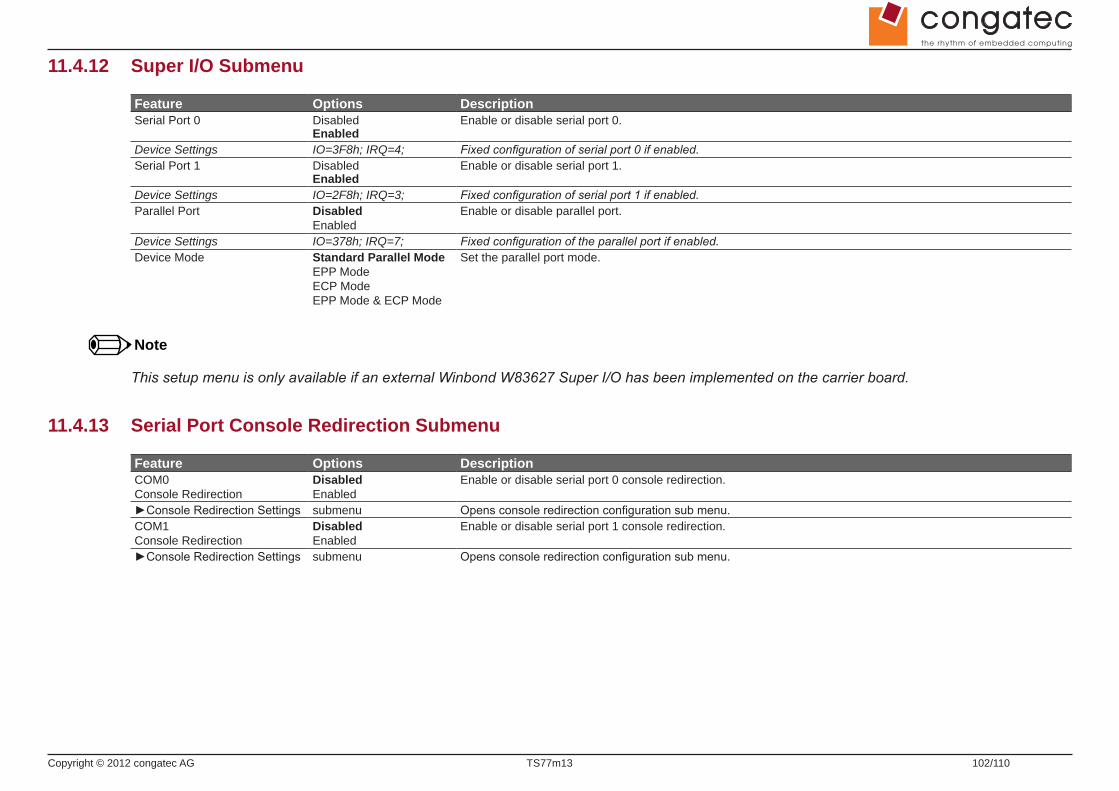
Copyright © 2012 congatec AG TS77m13 102/110
11.4.12 Super I/O Submenu
Feature Options DescriptionSerial Port 0 Disabled
EnabledEnable or disable serial port 0.
Device Settings IO=3F8h; IRQ=4; Fixed configuration of serial port 0 if enabled.Serial Port 1 Disabled
EnabledEnable or disable serial port 1.
Device Settings IO=2F8h; IRQ=3; Fixed configuration of serial port 1 if enabled.Parallel Port Disabled
EnabledEnable or disable parallel port.
Device Settings IO=378h; IRQ=7; Fixed configuration of the parallel port if enabled.Device Mode Standard Parallel Mode
EPP ModeECP ModeEPP Mode & ECP Mode
Set the parallel port mode.
Note
This setup menu is only available if an external Winbond W83627 Super I/O has been implemented on the carrier board.
11.4.13 Serial Port Console Redirection Submenu
Feature Options DescriptionCOM0 Console Redirection
DisabledEnabled
Enable or disable serial port 0 console redirection.
►Console Redirection Settings submenu Opens console redirection configuration sub menu.COM1 Console Redirection
DisabledEnabled
Enable or disable serial port 1 console redirection.
►Console Redirection Settings submenu Opens console redirection configuration sub menu.
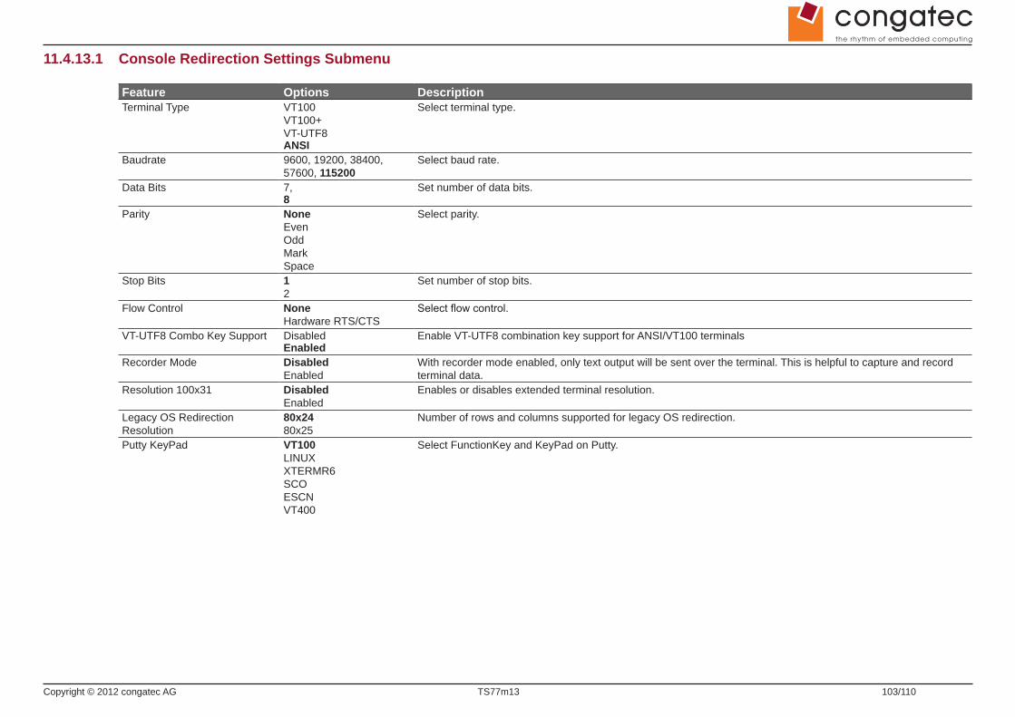
Copyright © 2012 congatec AG TS77m13 103/110
11.4.13.1 Console Redirection Settings Submenu
Feature Options DescriptionTerminal Type VT100
VT100+VT-UTF8ANSI
Select terminal type.
Baudrate 9600, 19200, 38400, 57600, 115200
Select baud rate.
Data Bits 7,8
Set number of data bits.
Parity NoneEvenOddMarkSpace
Select parity.
Stop Bits 12
Set number of stop bits.
Flow Control NoneHardware RTS/CTS
Select flow control.
VT-UTF8 Combo Key Support DisabledEnabled
Enable VT-UTF8 combination key support for ANSI/VT100 terminals
Recorder Mode DisabledEnabled
With recorder mode enabled, only text output will be sent over the terminal. This is helpful to capture and record terminal data.
Resolution 100x31 DisabledEnabled
Enables or disables extended terminal resolution.
Legacy OS Redirection Resolution
80x2480x25
Number of rows and columns supported for legacy OS redirection.
Putty KeyPad VT100LINUXXTERMR6SCOESCNVT400
Select FunctionKey and KeyPad on Putty.
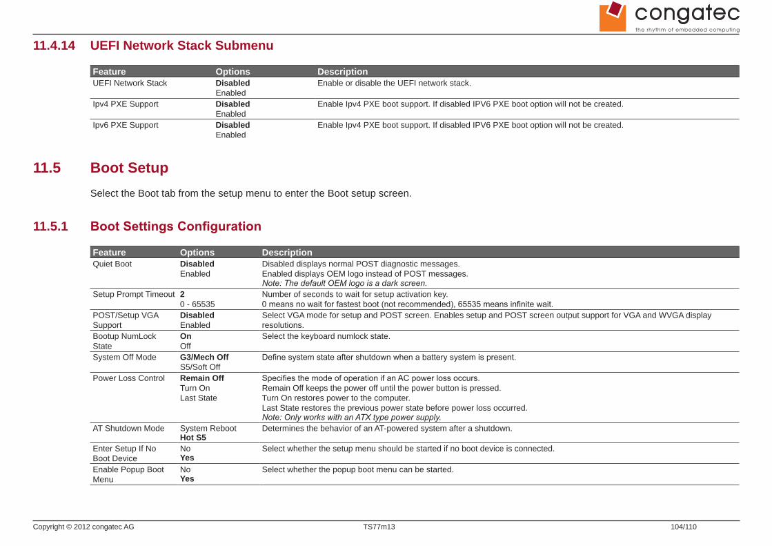
Copyright © 2012 congatec AG TS77m13 104/110
11.4.14 UEFI Network Stack Submenu
Feature Options DescriptionUEFI Network Stack Disabled
EnabledEnable or disable the UEFI network stack.
Ipv4 PXE Support DisabledEnabled
Enable Ipv4 PXE boot support. If disabled IPV6 PXE boot option will not be created.
Ipv6 PXE Support DisabledEnabled
Enable Ipv4 PXE boot support. If disabled IPV6 PXE boot option will not be created.
11.5 Boot SetupSelect the Boot tab from the setup menu to enter the Boot setup screen.
11.5.1 Boot Settings Configuration
Feature Options DescriptionQuiet Boot Disabled
EnabledDisabled displays normal POST diagnostic messages.Enabled displays OEM logo instead of POST messages.Note: The default OEM logo is a dark screen.
Setup Prompt Timeout 20 - 65535
Number of seconds to wait for setup activation key.0 means no wait for fastest boot (not recommended), 65535 means infinite wait.
POST/Setup VGA Support
DisabledEnabled
Select VGA mode for setup and POST screen. Enables setup and POST screen output support for VGA and WVGA display resolutions.
Bootup NumLock State
OnOff
Select the keyboard numlock state.
System Off Mode G3/Mech OffS5/Soft Off
Define system state after shutdown when a battery system is present.
Power Loss Control Remain OffTurn OnLast State
Specifies the mode of operation if an AC power loss occurs.Remain Off keeps the power off until the power button is pressed.Turn On restores power to the computer.Last State restores the previous power state before power loss occurred.Note: Only works with an ATX type power supply.
AT Shutdown Mode System RebootHot S5
Determines the behavior of an AT-powered system after a shutdown.
Enter Setup If No Boot Device
NoYes
Select whether the setup menu should be started if no boot device is connected.
Enable Popup Boot Menu
NoYes
Select whether the popup boot menu can be started.
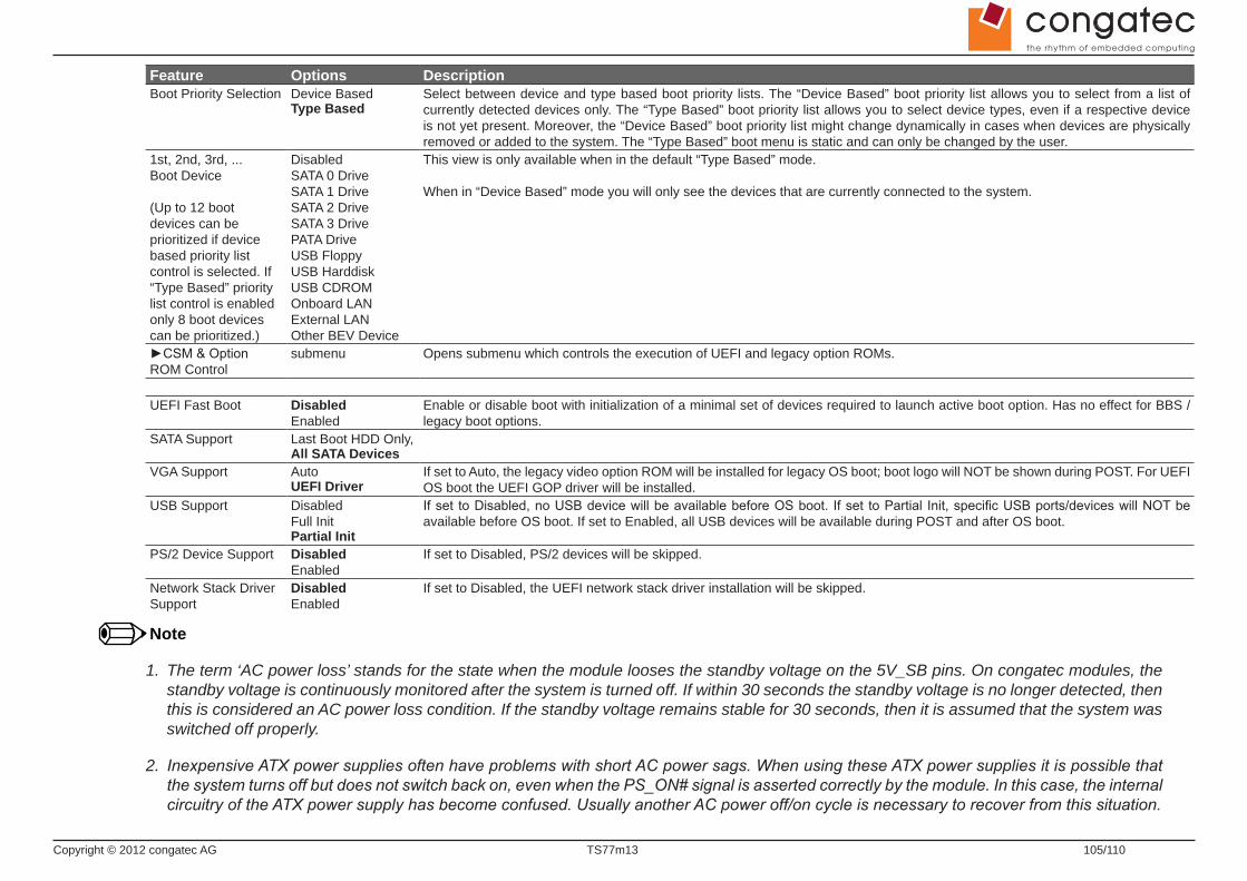
Copyright © 2012 congatec AG TS77m13 105/110
Feature Options DescriptionBoot Priority Selection Device Based
Type BasedSelect between device and type based boot priority lists. The “Device Based” boot priority list allows you to select from a list of currently detected devices only. The “Type Based” boot priority list allows you to select device types, even if a respective device is not yet present. Moreover, the “Device Based” boot priority list might change dynamically in cases when devices are physically removed or added to the system. The “Type Based” boot menu is static and can only be changed by the user.
1st, 2nd, 3rd, ... Boot Device (Up to 12 boot devices can be prioritized if device based priority list control is selected. If “Type Based” priority list control is enabled only 8 boot devices can be prioritized.)
DisabledSATA 0 DriveSATA 1 DriveSATA 2 DriveSATA 3 DrivePATA DriveUSB FloppyUSB HarddiskUSB CDROMOnboard LANExternal LANOther BEV Device
This view is only available when in the default “Type Based” mode.
When in “Device Based” mode you will only see the devices that are currently connected to the system.
►CSM & Option ROM Control
submenu Opens submenu which controls the execution of UEFI and legacy option ROMs.
UEFI Fast Boot DisabledEnabled
Enable or disable boot with initialization of a minimal set of devices required to launch active boot option. Has no effect for BBS / legacy boot options.
SATA Support Last Boot HDD Only, All SATA Devices
VGA Support AutoUEFI Driver
If set to Auto, the legacy video option ROM will be installed for legacy OS boot; boot logo will NOT be shown during POST. For UEFI OS boot the UEFI GOP driver will be installed.
USB Support DisabledFull InitPartial Init
If set to Disabled, no USB device will be available before OS boot. If set to Partial Init, specific USB ports/devices will NOT be available before OS boot. If set to Enabled, all USB devices will be available during POST and after OS boot.
PS/2 Device Support DisabledEnabled
If set to Disabled, PS/2 devices will be skipped.
Network Stack Driver Support
DisabledEnabled
If set to Disabled, the UEFI network stack driver installation will be skipped.
Note
1. The term ‘AC power loss’ stands for the state when the module looses the standby voltage on the 5V_SB pins. On congatec modules, the standby voltage is continuously monitored after the system is turned off. If within 30 seconds the standby voltage is no longer detected, then this is considered an AC power loss condition. If the standby voltage remains stable for 30 seconds, then it is assumed that the system was switched off properly.
2. Inexpensive ATX power supplies often have problems with short AC power sags. When using these ATX power supplies it is possible that the system turns off but does not switch back on, even when the PS_ON# signal is asserted correctly by the module. In this case, the internal circuitry of the ATX power supply has become confused. Usually another AC power off/on cycle is necessary to recover from this situation.
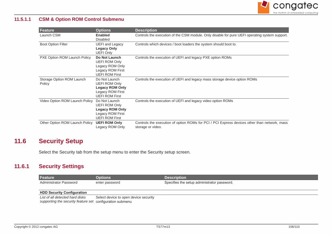
Copyright © 2012 congatec AG TS77m13 106/110
11.5.1.1 CSM & Option ROM Control Submenu
Feature Options DescriptionLaunch CSM Enabled
DisabledControls the execution of the CSM module. Only disable for pure UEFI operating system support.
Boot Option Filter UEFI and LegacyLegacy OnlyUEFI Only
Controls which devices / boot loaders the system should boot to.
PXE Option ROM Launch Policy Do Not LaunchUEFI ROM OnlyLegacy ROM OnlyLegacy ROM FirstUEFI ROM First
Controls the execution of UEFI and legacy PXE option ROMs
Storage Option ROM Launch Policy
Do Not LaunchUEFI ROM OnlyLegacy ROM OnlyLegacy ROM FirstUEFI ROM First
Controls the execution of UEFI and legacy mass storage device option ROMs
Video Option ROM Launch Policy Do Not LaunchUEFI ROM OnlyLegacy ROM OnlyLegacy ROM FirstUEFI ROM First
Controls the execution of UEFI and legacy video option ROMs
Other Option ROM Launch Policy UEFI ROM OnlyLegacy ROM Only
Controls the execution of option ROMs for PCI / PCI Express devices other than network, mass storage or video.
11.6 Security SetupSelect the Security tab from the setup menu to enter the Security setup screen.
11.6.1 Security Settings
Feature Options DescriptionAdministrator Password enter password Specifies the setup administrator password.
HDD Security ConfigurationList of all detected hard disks supporting the security feature set
Select device to open device security configuration submenu

Copyright © 2012 congatec AG TS77m13 107/110
11.6.2 Hard Disk Security
This feature enables the users to set, reset or disable passwords for each hard drive in Setup without rebooting. If the user enables password support, a power cycle must occur for the hard drive to lock using the new password. Both user and master password can be set independently however the drive will only lock if a user password is installed.
11.6.3 Save & Exit Menu
Select the Save & Exit tab from the setup menu to enter the Save & Exit setup screen.
You can display a Save & Exit screen option by highlighting it using the <Arrow> keys.
Feature DescriptionSave Changes and Exit Exit setup menu after saving the changes. The system is only reset if settings have been changed.Discard Changes and Exit Exit setup menu without saving any changes.Save Changes and Reset Save changes and reset the system.Discard Changes and Reset Reset the system without saving any changes.Save OptionsSave Changes Save changes made so far to any of the setup options. Stay in setup menu.Discard Changes Discard changes made so far to any of the setup options. Stay in setup menu.Restore Defaults Restore default values of all the setup options.Boot OverrideList of all boot devices currently detected. Select device to leave setup menu and boot from the selected device. Only visible and active if Boot Priority
Selection setup node is set to “Device Based”.
Copyright © 2012 congatec AG TS77m13 108/110
12 Additional BIOS FeaturesThe conga-TS77 uses a congatec/AMI AptioEFI that is stored in an onboard Flash Rom chip and can be updated using the congatec System Utility, which is available in a DOS based command line, Win32 command line, Win32 GUI, and Linux version.
The BIOS displays a message during POST and on the main setup screen identifying the BIOS project name and a revision code. The initial production BIOS is identified as BQ77R1xx or BH77R1xx where:
• BQ77 is the BIOS for modules with the QM77 chipset
• BH77 is the BIOS for modules with the HM76 chipset
• R is the identifier for a BIOS ROM file, 1 is the so called feature number and xx is the major and minor revision number.
The size of the conga-TS77 BIOS binary for both the QM77 and the HM76 variants is approximately 8 MB.
12.1 Supported Flash DevicesThe conga-TS77 supports the following flash devices:
• Spansion S25FL064K0SMFI01
• Winbond W25Q64CVSSIG
The flash devices listed above can be used on the carrier board for external BIOS support. For more information about external BIOS support, refer to the Application Note AN7_External_BIOS_Update.pdf on the congatec website at http://www.congatec.com.
12.2 Updating the BIOSBIOS updates are often used by OEMs to correct platform issues discovered after the board has been shipped or when new features are added to the BIOS.
For more information about “Updating the BIOS” refer to the user’s guide for the congatec System Utility, which is called CGUTLm1x.pdf and can be found on the congatec AG website at www.congatec.com.
Copyright © 2012 congatec AG TS77m13 109/110
12.3 BIOS Security FeaturesThe BIOS provides a setup administrator password that limits access to the BIOS setup menu.
12.4 Hard Disk Security FeaturesHard Disk Security uses the Security Mode feature commands defined in the ATA specification. This functionality allows users to protect data using drive-level passwords. The passwords are kept within the drive, so data is protected even if the drive is moved to another computer system.
The BIOS provides the ability to ‘lock’ and ‘unlock’ drives using the security password. A ‘locked’ drive will be detected by the system, but no data can be accessed. Accessing data on a ‘locked’ drive requires the proper password to ‘unlock’ the disk.
The BIOS enables users to enable/disable hard disk security for each hard drive in setup. A master password is available if the user can not remember the user password. Both passwords can be set independently however the drive will only lock if a user password is installed. The max length of the passwords is 32 bytes.
During POST each hard drive is checked for security mode feature support. In case the drive supports the feature and it is locked, the BIOS prompts the user for the user password. If the user does not enter the correct user password within four attempts, the user is notified that the drive is locked and POST continues as normal. If the user enters the correct password, the drive is unlocked until the next reboot.
In order to ensure that the ATA security features are not compromised by viruses or malicious programs when the drive is typically unlocked, the BIOS disables the ATA security features at the end of POST to prevent their misuse. Without this protection it would be possible for viruses or malicious programs to set a password on a drive thereby blocking the user from accessing the data.
Copyright © 2012 congatec AG TS77m13 110/110
13 Industry SpecificationsThe list below provides links to industry specifications that apply to congatec AG modules.
Specification LinkLow Pin Count Interface Specification, Revision 1.0 (LPC) http://developer.intel.com/design/chipsets/industry/lpc.htmUniversal Serial Bus (USB) Specification, Revision 2.0 http://www.usb.org/homePCI Specification, Revision 2.3 http://www.pcisig.com/specificationsSerial ATA Specification, Revision 3.0 http://www.serialata.orgPICMG® COM Express Module™ Base Specification http://www.picmg.org/PCI Express Base Specification, Revision 2.0 http://www.pcisig.com/specifications