columbia university in the city of new york · columbia university in the city of new york...
TRANSCRIPT

Columbia University in the City of New York
Condensed Matter physics
Horst StormerAron PinczukTony HeinzPhillip KimAndy MillisIgor Aleiner
Chemistry and Materials
Jack Norton David Reichman Jim Leighton Laura KaufmanColin NuckollsVirginia CornishDavid AdamsDalibor SamesBrian GibneyStephen O'Brien
Recent Faculty Hires:

Chemistry and Physics of Semiconductor Nanocrystals
Louis BrusChemistry DepartmentColumbia University
HistorySynthesis and self-assembly into solidsElectronic Structure and LuminescenceOptical Spectra of Single NanocrystalsCharge State of Single Nanocrystals.
NSF Nanocenter on Electrical Conductivity of Single Molecules and Carbon Nanotubes

What is a CdSe nanocrystal?
- Organic molecules ‘cap’ the outer surface of core semiconductor. They prevent aggregation, oxidation, and stabilize nanoparticles in the solution. Most important, they electronically isolate the particles and passivate the surface states.
0
20
40
60
80
0 5 10 15 20Diameter (nm)
% S
urfa
ce a
tom
s
CdSe
Chem
ical Potential
Xiaogang PengArkansas

1983

Synthesis 1986 Steigerwald etal, JACS 110, 3046 (1988)

Synthesis 1988 Bawendi etal J. Chem. Phys. 91, 7282 (1989)

ThermocoupleArgon gas at little above ambient pressure
Chemical synthesis of CdSe nanocrystals
- Narrow size distribution (~5%) is obtained by the fast injection of the chemical reagents into the flask at high temperature (~ 350 C).
- The precursors are prepared in the glove box to avoid oxygen and water.
0
Semiconductor: CdSe, CdTe, PbSe, etc.Metal: PtFe

100 nm
5 nm5 n5 nm
TEM images of PbSe quantum cubes after size selection (reaction temperature 215oC), size ~12 nm
Change of shape from spheric to cubic in the size regime of 8 to 11 nm
TEM of cubic PbSe nanocrystals
Chris Murray, Wolfgang Gaschler, Franz Redl, IBM-Columbia

3D solid structures
CoPt3 nanoparticles
Elena ShevchenkoO’Brien – MurrayColumbia-IBM

Bimodal superlattice of 11 nm magnetic Fe2O3 NCs and semiconducting 5 nm PbSe NCs
Redl, Cho, Murray, O’Brien Nature 423, 968 (2003)

Shape Control via Kinetics and Thermodymanics
Xiaogang Peng Arkansas
Key Concept: Tuning Monomer Activity
Stephen O’Brien, Applied Physics, Columbia
Cubic FeOWuestite
CdSe rods and tetrapods

C. Murray and M. Bawendi

High Quantum Yield LuminescenceMore stable than dye moleculesPossible use in biological imaging
Size tunable luminescenceNarrow emission band

Q Dot Corporationwww.qdots.com
Published in Nature Biotechnology Online
Biological Imaging Applications


Simple Model for Electronic Structure: Quantum Size Effect
Eg
• Energy of HOMO-LUMO Blue Shifted from bulk band gap
k
E
|v>
|c>
electron wavelength λquantized in particle:k ~ n /R; n=1,2..
• Optical Spectra are Discrete and Size Dependent
• Model uses known bulk band structure, and ignores• bonding reconstruction on surfaces
E(k) ~ Eg + n2h2/(8meR2)+ n2h2/(8mhR2)
Electron Momentum mv=hk=h/λ

Quantum Size Effect including Electrostatics
L. Brus, J. Chem. Phys. 79, 5566 (1983); 80, 4403 (1983)

Why does an H passivated 1.3 nm silicon nanocrystal emit in the blue, but an 1.3 nm oxide shell passivated nanocrystal emit in the red?
Theory with H passivation
Experiment: 0xide passivated
Wolkin etal Phys Rev Lett 82, 197 (1999)
Failure of Quantum Model in Silicon Nanocrystals:
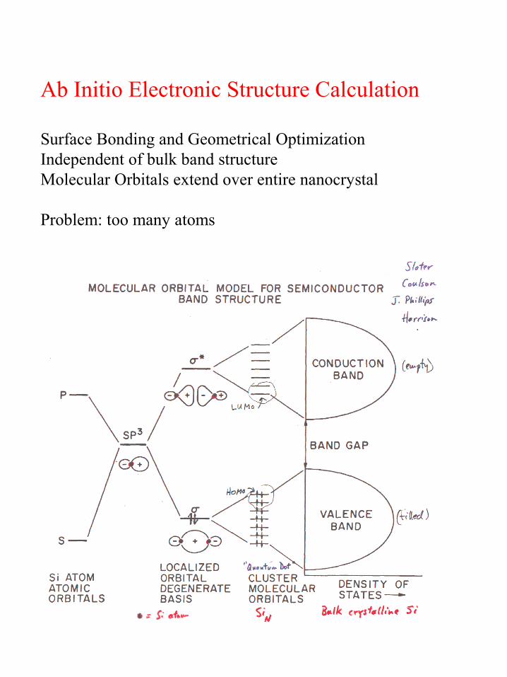
Ab Initio Electronic Structure Calculation
Surface Bonding and Geometrical OptimizationIndependent of bulk band structureMolecular Orbitals extend over entire nanocrystal
Problem: too many atoms

All electron Density Functional TheoryBecke B3YLP Hybrid Functional Structure completely optimized
Zhou, Friesner, Brus Nanoletters 3, 163 (2003)JACS 125, 15599 (2003)

-0.7
-0.6
-0.5
-0.4
-0.3
-0.2
-0.1
0.0
0.1
Si66O12(OH)40Si66H64
Orbital Energy(Hartree)
Molecular Orbitals of Si66 Species158 atoms, 468 normal modes, 1380 electrons
filled
empty
Oxide passivation lowers band gap by 1.5 eVLUMO moves downHOMO moves up
Fermi level unchanged; hardness decreases

HOMO pulled to surface by electronegative O atomsHOMO resides on weakened Si-Si back bonds

Bawendi group
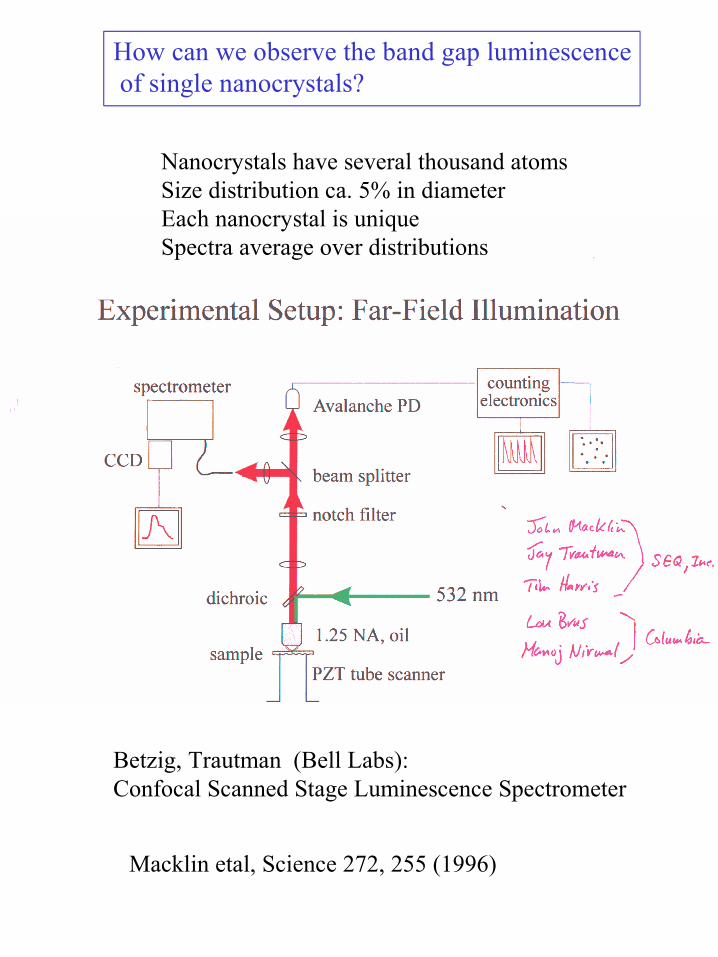
Nanocrystals have several thousand atomsSize distribution ca. 5% in diameterEach nanocrystal is uniqueSpectra average over distributions
How can we observe the band gap luminescence of single nanocrystals?
Betzig, Trautman (Bell Labs):Confocal Scanned Stage Luminescence Spectrometer
Macklin etal, Science 272, 255 (1996)

Nirmal etal, Nature 383, 802 (1996)
Raster scan image
field of luminescingnanocrystals

Semiconductor Capped QDs
• EFM of CdS capped CdSe
B. O. Dabbousi, et al. (1997)
CdSe
CdSTOPO
ZnS
E
Spatial Coordinate
~0.9 eV
~0.9 eV~0.2 eV
~0.5 eV

Blinking rate increases at higher laser power
ZnS layer on surface slows down blinking rate
ZnS coated

Schematic Blinking Mechanism: Photoionization and Re-neutralization
Vacuum Level
Ef = 5.0 eV
Metal
EA ~2 eV
Eg > 4 eV
Insulator
EA ~ 4.8 eV
Eg ~ 2.0 eV
CdSe
Eg hν
A
B
A
B
Dark State: Ionized Nanocrystal with hole insideBright State: Neutral Nanocrystal

Direct Measurement of Electric Field Due to One Ionized Nanocrystal
Electric Force Microscopy Invention:
Wickramasinghe IBM
Martin etal, Appl. Phys. Lett. 52, 1103 (1988)E

V V V ttip dc ac= + sin( )ω
Oscillating Capacitor
Electrostatic Force F Q Qzcoul = 1 2
24πε
Energy Stored in a Capacitor U CV QC= =1
212
22
Capacitative Force2 2
22
1 1 12 2 2
dU d Q Q dC dCF Vdz dz C dz dzC
= − = − = =
When a voltage is applied to the tip it feels a sum of electrostatic andcapacitative forces. If there are static charges on the surface, imagecharges are induced in the metal tip.
F F F dCdz
V Q Qze cap coulomb= + = +1
2 42 1 2
2πε
( ) ( )21 ( ) sin( ) sin( )2 4s
ac s acCPDdc dcQdC V V V t Q CV CV tdz zω ωπε= + + − + +
( )2 22
22
1 1(( ) ) ( )2 2 412( ) sin( ) cos(2 )44
sac sCPD CPDdc dc
sac acCPDdc
QdC V V V Q C V Vdz zQ CdC dCV V V t V t
dz dzz
πε
ω ωπε
= + + − + +
+ + − +
V W W eCPD substrate tip= − −( ) / ( )
( )F ω (2 )F ω
A tmsin( )ω
Can we measure a single charge on a single nanocrystal?
Electric Force Microscopy EFM

CdSe/ZnS Charge Blinking on Graphite
1ω 2ω
400 nm
• Illuminated with 20 W/cm2 at 442 nm
•Direct observation of Charge Blinking provides evidence for photoionization mechanism of Luminescence Blinking
Krauss etal J. Phys. Chem. 2001, B105, 1725
Charge image Polarizability image

Evolution from molecules to solid state as size increases