coldfire computer final presentation josh hudgins randy jedlicka drew larson project staff:
Post on 21-Dec-2015
217 views
TRANSCRIPT

Coldfire Computer
Final Presentation
Josh Hudgins
Randy Jedlicka
Drew Larson
Project Staff:

Abstract The central objective for this project is to produce a better
lab for CPSC 462 students. With this in mind, several labs must be laid out as tasks for these students to perform. In summary, the main tasks that must be accomplished to
produce the ColdFire microcomputer, for these labs, are the following:
Design Modification/Inspection of previous PROTEL layouts produced by Legendary Group 5
Production of PCB by 3rd party manufacturer Assemblage of components to completed PCB Programming of Flash Memory with “monitor”
program via JTAG connector Porting of VxWorks OS to Flash Memory
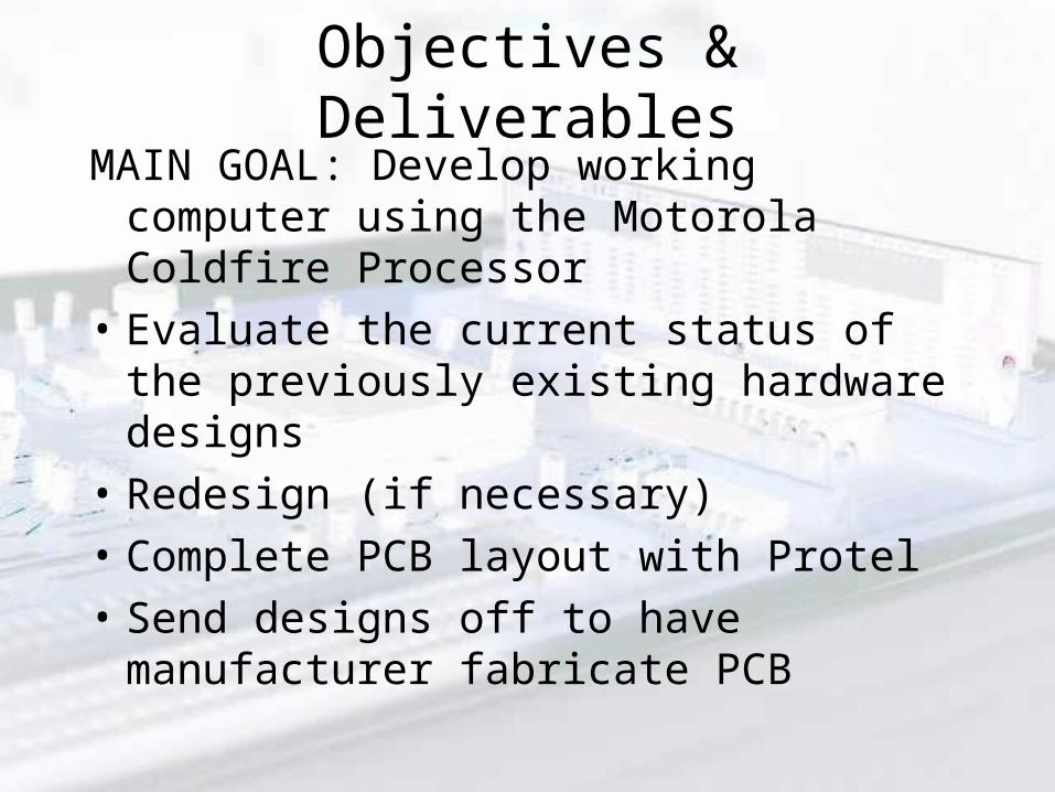
Objectives & Deliverables
MAIN GOAL: Develop working computer using the Motorola Coldfire Processor
• Evaluate the current status of the previously existing hardware designs
• Redesign (if necessary)
• Complete PCB layout with Protel
• Send designs off to have manufacturer fabricate PCB

Objectives & Deliverables (cont.)
• Mount all components onto board
• Port dBug monitor to Flash ROM
• Port VxWorks to Flash ROM
• Test Completed design with Dumb Terminal
• Rewrite Labs for CPSC 462

Evaluate/Redesign existing hardware designs in Protel
• Component change
– Flash: AM29F040 Vs NEC EEPROM
• Schematic Corrections
– Power line connected to ground?
– New lines for new flash
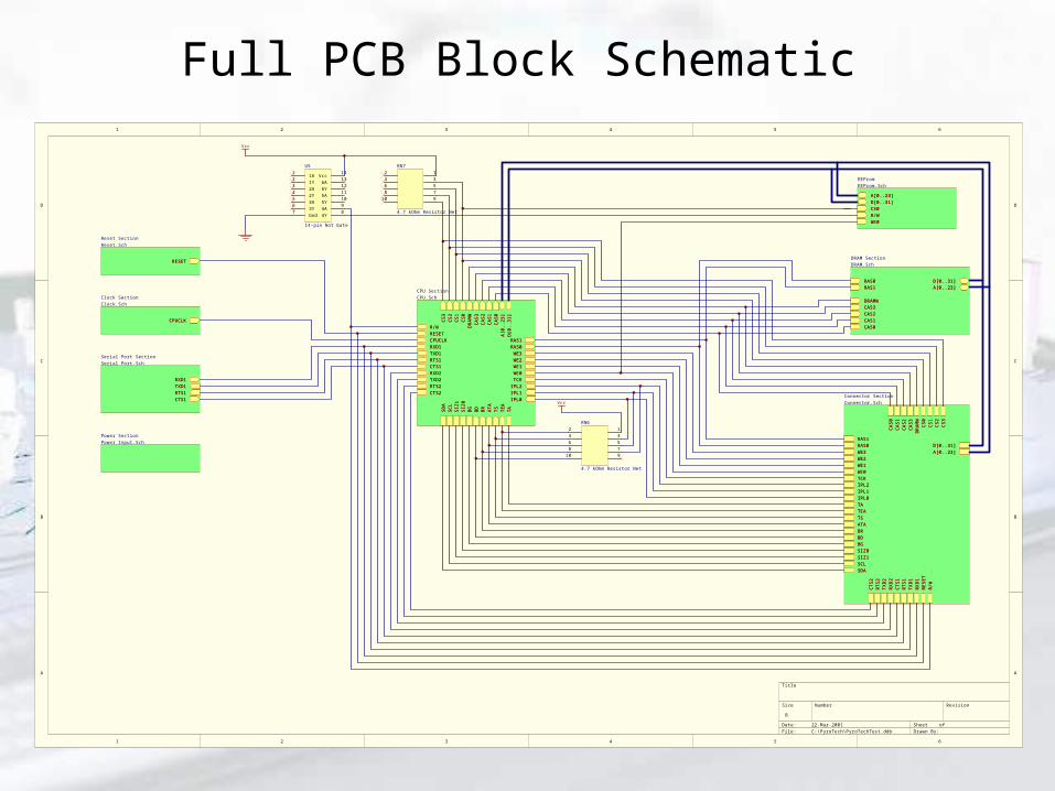
Full PCB Block Schematic
1 2 3 4 5 6
A
B
C
D
654321
D
C
B
A
Title
Number RevisionSize
B
Date: 22-Mar-2001 Sheet of File: C:\PyroTech\PyroTechTest.ddb Drawn By:
SDA
SCL
SIZ
1SI
Z0
BG
BD
BR
ATA
TS
TE
ATA
IPL0IPL1IPL2TCKWE0WE1WE2WE3RAS0RAS1
R/W
A[0
..23
]C
AS0
CA
S1C
AS2
CA
S3D
RA
MW
CS0
CS1
CS2
CS3
D[0
..31
]
CPUCLKRESET
RXD1TXD1RTS1CTS1RXD2TXD2RTS2CTS2
CPU SectionCPU.Sch
SDA
SCL
SIZ
1SI
Z0
BG
BD
BR
ATA
TS
TE
ATA
IPL0IPL1IPL2TCKWE0WE1WE2WE3RAS0RAS1
R/W
A[0
..23
]C
AS0
CA
S1C
AS2
CA
S3D
RA
MW
CS0
CS1
CS2
CS3
D[0
..31
]
CPUCLKRESET
RXD1TXD1RTS1CTS1RXD2TXD2RTS2CTS2
Power SectionPower Input.Sch
CS1
CS2
CS3
DR
AM
W
CA
S1C
AS0
CS0
CA
S3
D[0..31]
CA
S2
WE3
WE1WE0
IPL2IPL1
TAIPL0
TCK
RAS1RAS0
WE2
RT
S2C
TS2
TX
D2
RX
D2
RT
S1T
XD
1R
XD
1R
ESE
T
CT
S1
TSATA
BD
SCL
A[0..23]
SDA
SIZ1
R/W
SIZ0BG
BR
TEA
Connector SectionConnector.Sch
CS1
CS2
CS3
DR
AM
W
CA
S1C
AS0
CS0
CA
S3
D[0..31]
CA
S2
WE3
WE1WE0
IPL2IPL1
TAIPL0
TCK
RAS1RAS0
WE2
RT
S2C
TS2
TX
D2
RX
D2
RT
S1T
XD
1R
XD
1R
ESE
T
CT
S1
TSATA
BD
SCL
A[0..23]
SDA
SIZ1
R/W
SIZ0BG
BR
TEA
357910
864
12RN6
4.7 kOhm Resistor Net
Vcc
CAS0CAS1CAS2CAS3DRAMW
RAS0RAS1
D[0..31]A[0..23]
DRAM SectionDRAM.Sch
CAS0CAS1CAS2CAS3DRAMW
RAS0RAS1
D[0..31]A[0..23]
RXD1TXD1RTS1CTS1
Serial Port SectionSerial Port.Sch
RXD1TXD1RTS1CTS1
CPUCLK
Clock SectionClock.Sch
CPUCLK
Vcc14
6A13
6Y12
5A11
5Y10
4A9
4Y8
Gnd7
3Y6
3A5
2Y4
2A3
1Y2
1A1
U5
14-pin Not Gate
357910
864
12RN7
4.7 kOhm Resistor Net
RESET
Reset SectionReset.Sch
RESET
Vcc
A[0..23]D[0..31]CS0R/WWE0
EEPromEEProm.Sch
A[0..23]D[0..31]CS0R/WWE0

PCB Layout
• Completely redone
– Board dimension
– Layers of the board
– Component placement
– Trace routing
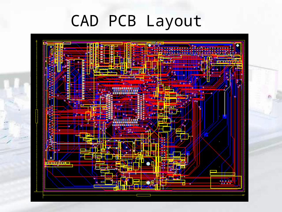
CAD PCB Layout
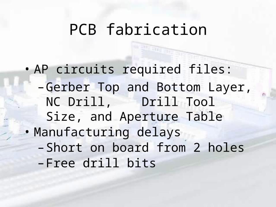
PCB fabrication
• AP circuits required files:
– Gerber Top and Bottom Layer, NC Drill, Drill Tool Size, and Aperture Table
• Manufacturing delays– Short on board from 2 holes– Free drill bits
Mounting components on PCB
• 160-pin processor socket
• The 96-pin Connector
• The BDM Connector
• Resistors and Capacitors
• Power ports
• The Under Voltage Sensor

Completed PCB
dBug Monitor Development Environment
• Win32 and SunOS versions• Directory Structure• Use of Makefiles• Problematic Issues
– Compiler Problems (EGCS1.1.1)– Makefile Issues– Board Specific Matters

dBug Monitor Development Environment (cont)
• Board Specific Monitor Program
– Adapted MCF5206AN
• Compiled Using Make Files

Write dBug Monitor Program

dBug Monitor ProgramPort into memory by use of JTAG

Port dBug Monitor to Flash
• JTAG Boundary Scan Technology
– Specific Files Needed• Protel - Netlist
• Motorola - BSDL– Converted to EDIF (Electronic Design Interchange
Format)
• Component File
• Sel File - Directory Structure
Port dBug Monitor to Flash
• Installation Problems
– WindowsNT / Windows2000
– Device Recognition
• Incompatible Protel file
• Error: No BST devices in design

Port dBug Monitor to Flash(Results)
• Placed DBUG monitor program in JBC3710
• Performed integrity checks of Monitor program
– Successful
• Continuing to resolve JTAG programming issues with Technical Support Personnel
VxWorks Operating System
• The BSP for the SBC5206 board sent to us by Wind River
• Unattempted: The OS will be ported to the board via serial port and dBug monitor program
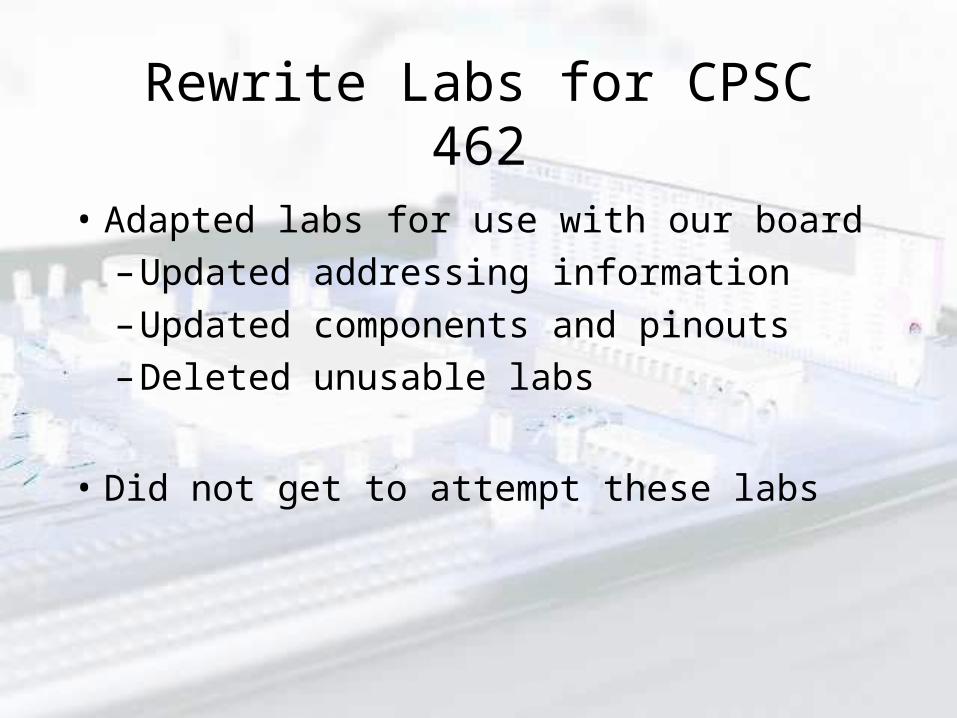
Rewrite Labs for CPSC 462
• Adapted labs for use with our board
– Updated addressing information
– Updated components and pinouts
– Deleted unusable labs
• Did not get to attempt these labs

Proposed Project Schedule
Week Date Description1 02/05/01 Proposal and Presentation2 02/12/01 Evaluate existing hardware designs, begin work on required assembly
routines for components3 02/19/01 Redesign existing hardware modules using Protel (if necessary) and
add new design for the Flash memory chosen4 02/26/01 Produce the final Printed Circuit Board layout, send off to be printed5 03/05/01 Continue work on required assembly routines for components6 03/12/01 **Spring Break**7 03/19/01 Mount hardware components onto board8 03/26/01 Load the monitor program, burn memory components with assembly
routines9 04/02/01 Port VxWorks into Flash memory10 04/09/01 Continue OS port11 04/16/01 Compile labs for 462 use12 04/23/01 Preparing for the final report13 04/30/00 Final demo and presentation
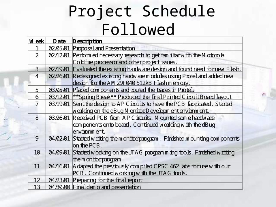
Project Schedule FollowedWeek Date Description
1 02/05/01 Proposal and Presentation2 02/12/01 Performed necessary research to get familiar with the Motorola
Coldfire processor and other project issues.3 02/19/01 Evaluated the existing hardware design and found need for new Flash.4 02/26/01 Redesigned existing hardware modules using Protel and added new
design for the AM29F040 512kB Flash memory.5 03/05/01 Placed components and routed the traces in Protel.6 03/12/01 **Spring Break** Produced the final Printed Circuit Board layout7 03/19/01 Sent the design to AP Circuits to have the PCB fabricated. Started
working on the dBug Monitor Development envirnment.8 03/26/01 Received PCB from AP Circuits. Mounted some hardware
components onto board. Continued working with the dBugenvironment.
9 04/02/01 Started writing the monitor program. Finished mounting componentson the PCB.
10 04/09/01 Started working on the JTAG programming tools. Finished writingthe monitor program
11 04/16/01 Adapted the previously compiled CPSC 462 labs for use with ourPCB. Continued working with the JTAG tools.
12 04/23/01 Preparing for the final report13 04/30/00 Final demo and presentation
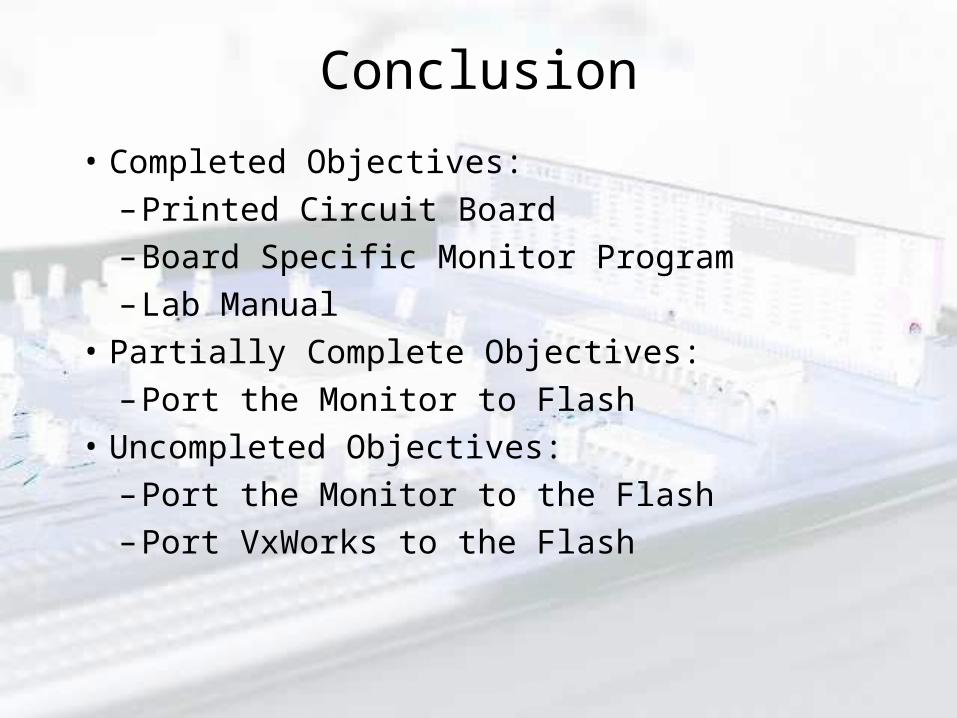
Conclusion
• Completed Objectives:– Printed Circuit Board– Board Specific Monitor Program– Lab Manual
• Partially Complete Objectives:– Port the Monitor to Flash
• Uncompleted Objectives:– Port the Monitor to the Flash– Port VxWorks to the Flash