coil misalignment compensation techniques for …
TRANSCRIPT

COIL MISALIGNMENT COMPENSATIONTECHNIQUES FOR WIRELESS POWER TRANSFER
LINKS IN BIOMEDICAL IMPLANTS
BY FANPENG KONG
A thesis submitted to the
Graduate School—New Brunswick
Rutgers, The State University of New Jersey
in partial fulfillment of the requirements
for the degree of
Master of Science
Graduate Program in Electrical and Computer Engineering
Written under the direction of
Professor Laleh Najafizadeh
and approved by
New Brunswick, New Jersey
October, 2015

ABSTRACT OF THE THESIS
Coil Misalignment Compensation Techniques for Wireless
Power Transfer Links in Biomedical Implants
by Fanpeng Kong
Thesis Director: Professor Laleh Najafizadeh
Wireless power Transfer (WPT) technique, based on inductive links, has been admit-
ted as a promising solution for powering biomedical implants. Ensuring a stable power
delivery via inductive links in implants under all conditions, however, has been a chal-
lenging design problem. One of the issues that negatively impacts the performance
of wireless power transfer (WPT) links in implants, is the misalignment in the posi-
tion of the transmitter and receiver coils, which could naturally occur as a result of
body movement or changes in the biological environment. An immediate effect of coil
misalignment is the change in coupling factor, resulting in the reduction of the power
delivered to the load at the receiver side.
In this work, we present a design concept that could be employed on the transmitter
side to mitigate this effect while keeping the driver to work at its optimum operating
condition. Specifically, we will demonstrate, analytically and through simulations, that
tuning the shunt capacitor and the supply voltage at the transmitter side could be
ii

a promising approach for compensating the performance degradation induced by coil
misalignment in WPT links.
iii

Acknowledgements
I would like to express my sincere gratitude towards a number of individuals whose
support, help and love have led me to reach this successful destination.
Firstly, I would like to thank my supervisor Dr. Laleh Najafizadeh for her patience
guidance and encouragement. Her help and advice opened my vision and led me to
reach several achievements during my journey in Rutgers University. The work can-
not be finished without her insightful comments. My sincere gratitude will go to her
again.
I would like to give my thank to my parents for their endless support and love. No
matter what things happened, they always encouraged me to live strongly and face the
difficulties positively. They gave me all they have to support me to pursue my dream
and never asked for the return. My thank will also express to my beloved soul mate,
Xinru, for her understanding and never-ending support. Her love has been the source
of my motivation and strength.
Last but no the least, my thank will go to my friends for their help in my life. Also,
I would like to thank my lab colleagues, Li Zhu and Yi Huang who are also my elder
brothers for encouraging and helping me during my time in Rutgers University.
This work was supported in part by the National Science Foundation (NSF) under grant
1408202, and by a fellowship from the ECE Department at Rutgers University.
iv

Table of Contents
Abstract . . . . . . . . . . . . . . . . . . . . . . . . . . . . . . . . . . . . . . . . ii
Acknowledgements . . . . . . . . . . . . . . . . . . . . . . . . . . . . . . . . . iv
List of Figures . . . . . . . . . . . . . . . . . . . . . . . . . . . . . . . . . . . . vii
1. Introduction . . . . . . . . . . . . . . . . . . . . . . . . . . . . . . . . . . . 1
1.1. Motivation and research objectives . . . . . . . . . . . . . . . . . . . . . 2
1.2. Organization of the Thesis . . . . . . . . . . . . . . . . . . . . . . . . . . 3
2. Wireless Power Transfer Technique . . . . . . . . . . . . . . . . . . . . . 4
2.1. The Categories of Wireless Power Transfer . . . . . . . . . . . . . . . . . 4
2.1.1. Near field wireless power transmission . . . . . . . . . . . . . . . 5
2.1.2. Far field wireless power transmission . . . . . . . . . . . . . . . . 10
2.1.3. Mid field wireless power transmission . . . . . . . . . . . . . . . . 12
2.2. Resonant coupling wireless power transfer structures . . . . . . . . . . . 13
2.2.1. 2-Coil based wireless power transfer structure . . . . . . . . . . . 13
2.2.2. 3-Coil based wireless power transfer structure . . . . . . . . . . . 16
2.2.3. 4-coil based wireless power transfer structure . . . . . . . . . . . 18
2.3. Conclusion . . . . . . . . . . . . . . . . . . . . . . . . . . . . . . . . . . 19
3. Coupled Coil Misalignment Analysis . . . . . . . . . . . . . . . . . . . . 20
3.1. Mathematical Model of Coils Misalignment . . . . . . . . . . . . . . . . 20
3.1.1. Misalignment analysis review . . . . . . . . . . . . . . . . . . . . 20
v

3.1.2. Mutual inductance analysis under misalignment . . . . . . . . . . 21
3.1.3. Calculation of mutual inductance . . . . . . . . . . . . . . . . . . 24
3.2. Conclusion . . . . . . . . . . . . . . . . . . . . . . . . . . . . . . . . . . 25
4. Misalignment Compensation Work Review . . . . . . . . . . . . . . . . 26
4.1. Frequency control methods . . . . . . . . . . . . . . . . . . . . . . . . . 27
4.2. Power supply control methods . . . . . . . . . . . . . . . . . . . . . . . . 28
4.3. Microcontroller control methods . . . . . . . . . . . . . . . . . . . . . . 31
4.4. Conclusion . . . . . . . . . . . . . . . . . . . . . . . . . . . . . . . . . . 31
5. Proposed Concept for Coils Misalignment Compensation . . . . . . . 33
5.1. Circuit Theory Analysis . . . . . . . . . . . . . . . . . . . . . . . . . . . 34
5.1.1. Receiver circuit . . . . . . . . . . . . . . . . . . . . . . . . . . . . 34
5.1.2. Reflected impedance theory . . . . . . . . . . . . . . . . . . . . . 37
5.1.3. Class E power amplifier . . . . . . . . . . . . . . . . . . . . . . . 40
5.2. Proposed Compensation Concept . . . . . . . . . . . . . . . . . . . . . . 45
5.2.1. Illustration of Misalignment Compensation Concept . . . . . . . 45
5.2.2. Simulation Results . . . . . . . . . . . . . . . . . . . . . . . . . . 47
5.2.3. Advantages of the proposed misalignment compensation design . 51
5.3. Conclusion . . . . . . . . . . . . . . . . . . . . . . . . . . . . . . . . . . 52
6. Conclusions . . . . . . . . . . . . . . . . . . . . . . . . . . . . . . . . . . . . 53
vi

List of Figures
2.1. The block diagram of wireless power transfer system. . . . . . . . . . . . 4
2.2. The categories of wireless power transfer techniques. . . . . . . . . . . . 5
2.3. The topology of capacitive wireless power transfer system. . . . . . . . . 6
2.4. Conceptual illustration of the inductive coupling wireless power transfer
technique. . . . . . . . . . . . . . . . . . . . . . . . . . . . . . . . . . . . 9
2.5. Resonance based wireless power transfer structure. . . . . . . . . . . . . 10
2.6. Structure of microwave wireless power transmission system. . . . . . . . 11
2.7. Circuit diagram of 2 coil wireless power transfer structure. . . . . . . . . 14
2.8. The comparison of received voltage across the load between resonant
structure and non-resonant structure [1]. . . . . . . . . . . . . . . . . . . 15
2.9. Circuit diagram of 3 coil wireless power transfer structure. . . . . . . . . 17
2.10. Circuit diagram of 4 coil wireless power transfer structure. . . . . . . . . 18
3.1. Conceptual illustration for coils with no misalignment. . . . . . . . . . . 22
3.2. Conceptual illustration for coils with angular misalignment. . . . . . . . 23
3.3. Conceptual illustration for coils with angular and axial misalignment. . 24
3.4. The order for functions to perform mutual inductance calculation [2]. . . 25
4.1. Frequency control compensation technique [3]. . . . . . . . . . . . . . . . 27
4.2. Closed loop gate control technique [4]. . . . . . . . . . . . . . . . . . . . 28
4.3. Closed loop power control technique [5]. . . . . . . . . . . . . . . . . . . 29
4.4. Closed loop power control technique implementing by a comparator and
RF transceiver [6]. . . . . . . . . . . . . . . . . . . . . . . . . . . . . . . 30
vii

4.5. Block diagram of microcontroller control technique [7]. . . . . . . . . . . 32
5.1. Adopted circuit model for wireless power transfer system. . . . . . . . . 33
5.2. Illustration of magnetic coupling working theory. . . . . . . . . . . . . . 35
5.3. The circuit diagram of WPT receiver. . . . . . . . . . . . . . . . . . . . 36
5.4. Equivalent circuit seen at the transmitter employing reflected impedance
theory. . . . . . . . . . . . . . . . . . . . . . . . . . . . . . . . . . . . . . 37
5.5. The circuit diagram for a simplified receiver in WPT system. . . . . . . 38
5.6. Circuit diagram of a basic class E power amplifier. . . . . . . . . . . . . 39
5.7. Calculated and simulated supply voltage values in WPT transmitter to
achieve compensation in presence of misalignment. . . . . . . . . . . . . 48
5.8. Calculated and simulated shunt capacitor values in WPT transmitter to
achieve compensation in presence of misalignment. . . . . . . . . . . . . 49
5.9. Simulated waveforms on the drivers drain voltage, Vds, and on the loads
peak voltage under optimum operation condition at k=0.3. . . . . . . . 50
5.10. Simulated waveforms on the drivers drain voltage, Vds, and on the loads
peak voltage under the presence of misalignment at k=0.28, no compen-
sation. . . . . . . . . . . . . . . . . . . . . . . . . . . . . . . . . . . . . . 50
5.11. Simulated waveforms on the drivers drain voltage, Vds, and on the loads
peak voltage under the presence of misalignment at k=0.28, with apply-
ing compensation. . . . . . . . . . . . . . . . . . . . . . . . . . . . . . . 51
viii

1
Chapter 1
Introduction
The interest in biomedical implants has been gaining momentum since they have found
applications in various domains such as: pacemakers [8] (to treat irregular hear beat),
cochlear prostheses [9] (assist the deaf people with hearing) and multichannel neural
recording systems [10] (for continuous monitoring of internal biosignal, namely, neu-
ral activities). Finding the optimum technique for delivering enough power to these
biomedical implants has been a subject of several investigations [11] [12]. Conven-
tionally, batteries are used to deliver the power, however, this approach offers several
limitations. For example, the size, limited storage capacity and the number of recharge
cycles render batteries as a non-ideal solution for powering biomedical implants as they
need to be replaced via surgery [13]. Wireless power transfer is an alternative solution,
which offers an attractive power delivery scheme for biomedical implants by limiting
the need for battery replacement.
One of the popular techniques used for the realization of the wireless power transfer
(WPT) scheme is inductive coupling [13]. The basic structure of this technique requires
two inductors, one (primary coil) which is placed externally as the transmitter and
another (secondary coil) which is placed inside the body at a short distance from the
primary coil as the receiver. The power transfer capability of this system is highly
depended on the coupling factor between the two coils [11]. However, the coils in
biomedical implants for power transfer can be misaligned due to the movement of body,

2
which decreases the coupling factor and adversely affects the WPT to implants. This
will deviate the driver of primary coil (class E power amplifier generally) from operating
at its optimum working condition. The power delivered to the load is also changed due
to the variance of the coupling factor. An ’ideal’ approach to address the misalignment
issue in WPT system of biomedical implants is to sense the changes induced by the
misalignment and automatically self-reconfigure to compensate the negative effect of
misalignment.
1.1 Motivation and research objectives
As one of the key factors which negatively affects the WPT system, the misalignment
issue needs to be addressed. Recently, different compensation methods have been pro-
posed. In [4], the working frequency of the system was suggested to be altered, which in
turn changes the power transfer efficiency via the inductive links [5]. In [3] the drain in-
ductor is tuned to mitigate the misalignment negative effect, but this approach requires
an additional block to change the inductor. The goal of this work is to develop a new
compensation concept to mitigate the misalignment issue without the disadvantages in
[4] [3].
The research motivation is described as above and the research objectives of this Thesis
is illustrated as follows. To eliminate the problems induced by the batteries in biomed-
ical implants, a resonance-based inductively coupled links needs to be developed. An
analytical study on misalignment needs to be performed to show its effect on the in-
ductive links. The misalignment induced issue on the class E power amplifier and
the power delivered to the load should be analyzed to identify the specific problems.
After acknowledging the problems, a design method needs to be proposed for solving
them.

3
1.2 Organization of the Thesis
In chapter 2, the theory behind the wireless power transfer technique is introduced in
detail. The basic structure of wireless power transfer is also illustrated. The technique
is classified into three categories based on the power transfer distance namely, near,
mid and far field wireless power transfer.
In Chapter 3, different scenarios of the coil misalignment are discussed. To analyze
these situations, the analytical method for coil misalignment are also presented in this
chapter.
In Chapter 4, the existing work regrading the coil misalignment compensation methods
at the transmitter or the receiver side.
In Chapter 5, the proposed misalignment concept is presented and its performance is
verified through simulations.
Finally, the conclusion and summary of this Thesis are given in Chapter 6.

4
Chapter 2
Wireless Power Transfer Technique
The WPT technique, based on the transfer distance, can be classified into three cate-
gories: near, mid, and far wireless power transfer. In this chapter, these categories will
be reviewed. In addition, the theory behind wireless power transfer is presented in this
chapter. Besides these, different resonance-based wireless power transfer structures are
analyzed in detail.
Figure 2.1 The block diagram of wireless power transfer system.
2.1 The Categories of Wireless Power Transfer
The categories are classified based on the working distance, d, between the transmitter
and receiver, in the wireless power transfer system in Fig. 2.1. The illustration of these
categories is shown in Fig. 2.2. Suppose the wavelength of power transfer is λ, and the
transmission distance d is less than λ/2π, d < λ/2π, then the system is classified as

5
Figure 2.2 The categories of wireless power transfer techniques.
near field. If d is more than λ/π, d > λ/π, it is named as far field. The mid field is
classified as d is between λ/2π and d > λ/π, which is λ/2π < d < λ/π. The near field
WPT system is described first.
2.1.1 Near field wireless power transmission
In near field WPT, the basic power transmission approaches are magnetic induction
and electric induction. The next paragraphs will describe them separately.
Wireless power transfer through electric induction uses capacitive power transfer
(CPT) technique. Due to its small system volume and profile [14], CPT is used in small
sized applications such as biomedical applications [15] [16], robots and mobile devices
6
[17], [18]. In addition, the merits of a cheap and flexible design make the capacitive
power transfer to be an appropriate method in moving systems, such as robot arms
[19]. Even though the magnetic induction has the advantage of high power transfer
efficiency than capacitive power transfer, CPT is the better choice than the magnetic
induction under the high operational frequency scenarios [15]. The basic topology
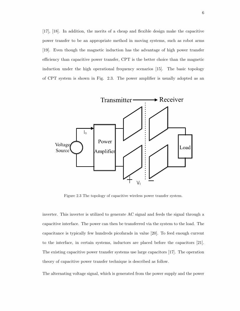
of CPT system is shown in Fig. 2.3. The power amplifier is usually adopted as an
Figure 2.3 The topology of capacitive wireless power transfer system.
inverter. This inverter is utilized to generate AC signal and feeds the signal through a
capacitive interface. The power can then be transferred via the system to the load. The
capacitance is typically few hundreds picofarads in value [20]. To feed enough current
to the interface, in certain systems, inductors are placed before the capacitors [21].
The existing capacitive power transfer systems use large capacitors [17]. The operation
theory of capacitive power transfer technique is described as follow.
The alternating voltage signal, which is generated from the power supply and the power

7
amplifier, is applied to the capacitor. It produces an electric field which can be modeled
as:
E =V
l. (2.1)
Here, V is the voltage applied on the two plates of the capacitor and l is the distance
between the two plates. The alternating voltage will induce an oscillating electric field
in the capacitor. Due to the electrostatic induction, the alternating electric field can
generate a variable potential on the receiver plate. Thus, an alternating current is
also generated to feed the load. The transmitted power depends on the frequency and
capacitance. In Fig. 2.3, the power which is going to be transferred to the load is
expressed as [14]:
P = VtIocos(β). (2.2)
In 2.2 Vt is the voltage across the two plates of transmitter capacitor and β is the
phase difference between the voltage Vt and the transmitter current Io. β and Io can
be derived as [14]:
β = tan−1(− 1
ωCRre), (2.3)
Io =Vt√
(1/ω2C2) +R2re
, (2.4)
where C is the capacitance, ω is the working frequency and the Rre is the reflected
impedance in the transmitter which is from the receiver. Then the voltage across each
capacitor then is found as:
VC =IoωC
. (2.5)
Equations (2.2)-(2.5) present the important design parameters. These design factors
can be optimized to achieve the best working condition of CPT system.
Currently, CPT is applied in some low power applications. For applications involving
high power transfer, the magnetic induction will be used. Additionally, electric fields
can interact strongly with some materials, such as human muscle [22]. Therefore, for

8
powering biomedical implants, the magnetic induction is more widely used instead of
electric induction.
Magnetic induction power transfer (MIWPT) is used to transfer power via mag-
netic field. The magnetic coupling can be defined as two groups, inductive wireless
power transfer (IWPT) and resonant wireless power transfer (RWPT) [23]. The induc-
tive wireless power transfer is realized by utilizing non-resonant coupled inductors, such
as a conventional transformer. It works on the principle of a primary coil generating a
magnetic field due to an AC current and inducing an alternating voltage in the receiver
coil. This technique requires that the magnetic field is covered by the receiver coil in
short distance and the presence of a magnetic core is necessary. The coupling between
the two coils is determined by the distance between the inductors, the shape and the
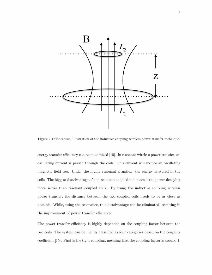
placement angle of the coils. The working theory of this technique is shown in Fig.
2.4. Here, L1 represents the transmitter coil which is typically to be made as large as
possible for transmitting more power. L2 is the receiver coil to receive the energy. B
indicates the magnetic field coupled by the two coils and Z is the distance to transfer
the power.
The resonant coupling method is considered to be the most efficient way in wireless
power transfer applications [15]. This method requires a resonant transformer. As for
the basic two resonator system, it has two high quality factor Q coils connected with
capacitors to form two coupled LC circuits. This structure is shown in Fig. 2.5. The
resistors Rs and Rc are used to model the parasitic resistors associated with the coils
Ls and Lc, respectively.
If these two resonators are placed in proximity to one another such that there is magnetic
coupling between them, it becomes possible that the resonators can exchange the energy
in high efficiency. When the two resonators work at the same resonant frequency, the
9
Figure 2.4 Conceptual illustration of the inductive coupling wireless power transfer technique.
energy transfer efficiency can be maximized [15]. In resonant wireless power transfer, an
oscillating current is passed through the coils. This current will induce an oscillating
magnetic field too. Under the highly resonant situation, the energy is stored in the
coils. The biggest disadvantage of non-resonant coupled inductors is the power decaying
more server than resonant coupled coils. By using the inductive coupling wireless
power transfer, the distance between the two coupled coils needs to be as close as
possible. While, using the resonance, this disadvantage can be eliminated, resulting in
the improvement of power transfer efficiency.
The power transfer efficiency is highly depended on the coupling factor between the
two coils. The system can be mainly classified as four categories based on the coupling
coefficient [15]. First is the tight coupling, meaning that the coupling factor is around 1.

10
Figure 2.5 Resonance based wireless power transfer structure.
Second is the overcoupling, it happens when the secondary coil is placed so close to the
primary coil. The third category is defined as critical coupling. It happens when the
power transfer is in its optimum passband. The last category is the loose coupling. It
can be seen from its name that in this situation, the coils are far away from each other
and the coupling coefficient is much less than the tight coupling. There are different
structures to build the resonant wireless power transfer. The detailed information which
includes the analysis will be discussed in section 2.2.
2.1.2 Far field wireless power transmission
For achieving power transmission over large distances, the far field wireless power trans-
fer technique is used. It is briefly introduced in this section . Two methods are usually
adopted in far field transmission which are microwave and optical electricity.
Microwave transmission uses microwave to transmit power over a long distance.
This technique should thank to Nikola Tesla who contributed to the design of modern
electricity supply system and demonstrated ’the power transmission without wires’ [24].
Basically, this power transmission technique can be divided into three blocks as shown
in Fig. 2.6 [25]. First block is to convert DC power to microwave power for making
it to be ready transferred. The second block is the link which is used to transfer the

11
Figure 2.6 Structure of microwave wireless power transmission system.
power. The last one is the receiver block to receive and rectify the power.
These blocks with their interaction determine the power transfer efficiency of the system.
For example, if the power transfer efficiency of each block in Fig 2.6 is represented by
η1, η2 and η3, the overall power transfer efficiency can be found as:
η = η1η2η3. (2.6)
For realizing the power transfer links required in this method, several techniques have
been adopted. One of them uses an active phased array [25]. This technique is applied
in very large arrays ,such as in space, for maximizing the power transfer efficiency.
Another technique, best suited for smaller system, is to combine an ellipsoidal reflector
and dual-mode horn. [25].
Optical electricity which uses laser beam, is considered to be another promising
approach for realizing the far field wireless power transfer. Even though the power is
transmitted using laser, in the receiver side the power still needs to be converted to the
electrical energy. There are several advantages for utilizing laser for power transmission
[26]:
1 The laser beam can be made as small as possible for small products application.
2 There is no radio frequency interfacing with other communication products such

12
as phone and wifi by using laser beam.
3 Using laster beam, the amount of transfer power can be controlled .
Even though there are many advantages, the drawbacks of this technique cannot be
ignored, which are listed as below:
1 The laser is dangerous even in low power level, it can cause blindness in people
and animals.
2 The efficiency for converting the power from light to electricity is low, resulting
much power wasted [26].
3 Optical wireless power transfer technique requires a direct line from the transmit-
ter to the target. It is not applicable in certain scenarios.
The far field power transfer technique is a promising way to transmit power wirelessly
over a large distance. However, in this thesis, the main discussion is the wireless power
transfer for biomedical application which is included in the near field transmission.
Therefore, the far field transmission was introduced briefly here. The next section is
going to discuss the mid field wireless power transfer.
2.1.3 Mid field wireless power transmission
Mid field power transfer is reported in a recent publication [27]. The power transfer
distance of mid field is between near field and far field. It has been approved that it will
generate high power transfer efficiency in mid field comparing to near field when the
receiver dimension is less than the transmitter [27]. Conventionally, most of the research
in near field wireless power transfer using magnetic field are based on applications that
use a frequency less than 10 MHz. However, when the receiver size is much smaller than
the transmitter, it results in a weak coupling and hence the inductively coupled coils

13
are inefficient at the lower frequency. Therefore, in [28], it was shown that by utilizing
a combination of inductive and radiative modes, higher power transfer efficiency can
be achieved in mid field. Also, higher efficiency is achieved by utilizing in low-giga
hertz range. However, in mid field wireless power transfer technique, one of the design
difficulties is the voltage source for achieving optimum power transfer efficiency.
This section mainly discussed the three categories of wireless power transfer system
based on the distance of the power transfer. In each category, the methods for real-
ization are also analyzed in detail. For biomedical implants, the near field is widely
used. The resonant power transfer is a preferred approach in biomedical applications.
Therefore, in the next section, the structures of resonant power transfer are well ana-
lyzed.
2.2 Resonant coupling wireless power transfer structures
In resonance coupling, there are mainly 3 structures: two-coil links, three coil links and
four coil links based on the number of coils used. These three structures are widely
used in today’s near field wireless power applications.
2.2.1 2-Coil based wireless power transfer structure
The two-coil based resonance coupling structure is shown in Fig. 2.7 [1]. A voltage
source is added at the transmitter with a source resistor Rs. On the transmitter side,
the resonator is formed by a capacitor C1 and the primary coil L1. There is also a
parasitic resistor R1, the primary coil at the transmitter side. The receiver resonator is
also formed by a capacitor Cp and the inductor L2. R2 is the parasitic resistor of L2.
The load is modeled by a resistor RL.

14
Figure 2.7 Circuit diagram of 2 coil wireless power transfer structure.
The current i1 which goes through the transmitter coil is a time variant current. It
generates a magnetic field. Through the mutual inductance M12 between the primary
and secondary coil, the magnetic field goes into L2 and generates the receiver current
i2. The power is transferred by this mechanism. To maximize the transferred power,
the working frequency of the transceiver LC resonators needs to be tuned to match
each other. The frequency fo is the resonance frequency of these two resonators:
fo =1
2π√L1C1
=1
2π√L2Cp
. (2.7)
In Fig. 2.7, the voltage across the load VL can be expressed as [1] :
VL =jωM12i1
1 + (jωL2 +R2)(1RL
+ jωCp). (2.8)
The authors of [1] compared the load voltage between the structure with resonator and
without resonator which indicates that C1 and Cp are removed in Fig. 2.7. Under the
no resonators situations, the voltage across the load V′L is modeled as [1]:
V′L =
jωM12i1
1 + jωL2+R2
RL
. (2.9)
From the result, it shows that in low frequency range, the voltages in both situations
are relatively the same. However, when the frequency goes up to get close to the

15
resonant frequency, the voltage of resonance coupling becomes higher than the inductive
coupling. Then as the frequency goes up, the voltage of inductive coupling is higher
than the resonance coupling which is shown in Fig. 2.8.
Figure 2.8 The comparison of received voltage across the load between resonant structure andnon-resonant structure [1].
By including the quality factor, the power transfer efficiency of the resonant links is
[1]
η =k12Q1Q2L
1 + k212Q1Q2L
Q2L
QL. (2.10)
Here, Q1 = ωL1R1
is the quality factor of the transmitter. ω is the operational angular
frequency of this system. The receiver quality factor is Q2 = ωL2R2
. The load quality
factor is expressed : QL = RLωL2
. Q2L = Q2QLQ2+QL
is the combination of Q2 and QL.
The detailed steps for generating the power transfer efficiency can be found in [1]. Even

16
though the two-coil based structure is widely used by the designers, the power transfer
efficiency is low. Therefore, 3-coil and 4-coil structures have been proposed to get
more power transfer efficiency. In the next section, the 3-coil structure will be briefly
discussed.
2.2.2 3-Coil based wireless power transfer structure
In [29], the three-coil based resonance wireless power transfer structure was successfully
implanted. The motivation of designing the three-coil structure is to achieve a high
power delivered to the load without hurting the power transfer efficiency because as it
will be seen, the four-coil based structure can reach a high power transfer efficiency,
but resulting in a low power received by the load.
Comparing with the two-coil structure, an additional resonator is added between the
transmitter and receiver to form three-coil power transfer structure. The circuit diagram
of three-coil structure is shown in Fig. 2.9. In this structure, the power transfer
efficiency η3coil can be expressed as [29]:
η3coil =(k223Q2Q3)(k
234Q3Q4L) + k224Q2Q2L
cos(θ)(1 + k234Q3Q4L)√A2 +B2
.Q4L
QL, (2.11)
where, A, B and θ are:
A = 1 + k223Q2Q3 + k234Q3Q4L + k224Q2Q2L, (2.12)
B = 2Q2Q3Q4Lk23k24k34, (2.13)
θ = tan−1(B/A). (2.14)
k is the coupling factor between the inductive coils. k23, k34 and k24 represent the
coupling factor of L2 and L3, L3 and L4, and L2 and L4 respectively. Q2, Q3, Q4 and
QL represent the quality factor of L2, L3, L4 and the load respectively.
Q2 = ωL2/R2. (2.15)

17
Figure 2.9 Circuit diagram of 3 coil wireless power transfer structure.
Q3 = ωL3/R3. (2.16)
QL = RL/ωL3. (2.17)
Q4 = ωL4/R4. (2.18)
Q4L is the combination of Q4 and QL, as:
Q4L = Q4QL/(Q4QL). (2.19)
Here ω represents the working frequency of these coils. The power delivered to the load,
PL, can be computed as:
PL =V 2s
2R2
(k223Q2Q3)(k234Q3Q4L) + k224Q2Q2L
A2 +B2.Q4L
QL. (2.20)
where Vs is the power source which comes from power supply and R2 is the parasitic
resistance of L2. Due to the large distance between L2 and L4, the coupling factor
k24 can be ignored, therefore the equations of power transfer efficiency η′3coil and power

18
delivered to the load P′L can be simplified as below:
η′3coil =
(k223Q2Q3)(k234Q3Q4L)
(1 + k234Q3Q4L + k223Q2Q3)(1 + k223Q2Q3).Q4L
QL, (2.21)
P′L =
V 2s
2R2
(k223Q2Q3)(k234Q3Q4L)
(1 + k234Q3Q4L + k223Q2Q3)2.Q4L
QL. (2.22)
The merits of this structure comparing with the 2-coil system are by adding additional
resonator between the primary and secondary coil, it provides another design freedom
to be adjusted to reach the optimum performance. Also, the parameters L3, L4 and
the coupling factor k34 can be utilized to form an impedance matching circuit. The
high power transfer efficiency can be achieved under any load RL. In addition, by
optimizing k23 and k34, the optimum power delivered to the load can be computed
based on (2.21).
2.2.3 4-coil based wireless power transfer structure
The four-coil structure in Fig. 2.10 has been widely used recently [29]. Comparing with
the 3-coil structure, four-coil links is achieved by adding another additional resonator
between the transmitter coil and receiver coil. It can mitigate the adversely affect of
the small coupling factors between the transceiver [29]. The basic four-coil structure
is shown in Fig. 2.10. Here the transmitter coil is modeled as L1 and the remain
Figure 2.10 Circuit diagram of 4 coil wireless power transfer structure.

19
components are similar to the ones in Fig. 2.9. The main goal of this structure is to
maximize the power transfer efficiency η4coil [13]. It can be expressed as:
η4coil =(k212Q1Q2)(k
223Q2Q3)(k
234Q3Q4)
[(1 + k212Q1Q2)(1 + k234Q3Q4) + k223Q2Q3][1 + k223Q2Q3 + k234Q3Q4]. (2.23)
The symbols Q1, Q2, Q3, Q4, k12, k23 and k34 in (2.22) have the similar expressions as
in (2.15). To achieve the goal of optimizing the power transfer efficiency, the quality
factors of this structure are needed to be designed as high as possible [13]. Also the
power transfer efficiency can be simplified as:
η′4coil =
k223Q2Q3
1 + k223Q2Q3. (2.24)
Based on (2.23), the quality factors of the transmitter coil and receiver coil do not
have a big impact on the power transfer efficiency. Therefore, by carefully design-
ing the primary and secondary coils, the maximize power transfer efficiency can be
obtained.
2.3 Conclusion
In this chapter, modern technique for wireless transferring power were reviewed. Based
on the power transfer distance, three categories of wireless power transmission are de-
fined. For the biomedical application, the near filed wireless power transmission is
widely used. The newly introducer mid field wireless power transfer technique was also
described in this chapter. Due to the advantages which introduced in this chapter, the
resonance structure has been adopted to be used for wireless power transfer in biomed-
ical implants. Different types of resonance coupling structures are introduced, which
are 2-coil, 3-coil and 4-coil resonance based wireless power transfer structures.

20
Chapter 3
Coupled Coil Misalignment Analysis
For biomedical applications, the inductively coupled coils in wireless power transfer are
designed to maximize the power transfer efficiency. Most of the studies work on the
ideal case that the inductive coils are perfectly aligned with each other. However, when
the receiver coils are implanted in the human body, the position of receiver coils can be
easily changed due to the movement of human body. This results in the misalignment
between transmitter coil and receiver coil. Coil misalignment changes the mutual in-
ductance of the coupled coils and effectively degrades the performance of the wireless
power transfer system, such as reducing the delivered power and the power transfer
efficiency. Therefore, the effect of the coils misalignment is important and needs to be
investigated.
In this chapter, we present the analysis of coils misalignment. Different misalignment
situations are discussed and the mutual inductance between the coupled coils under
misalignment is analyzed.
3.1 Mathematical Model of Coils Misalignment
3.1.1 Misalignment analysis review
In the inductive links, the primary coil generates magnetic field and the receiver coil
picks up a part of the magnetic field for power transfer. The system needs to be robust

21
enough for immunizing the misalignment. To obtain the optimum performance, the
coupled coils in the system has been carefully designed. For example, the design in
[30] focused on steady-state circuits analysis and the results were validated by experi-
ment.
Some work presented the analysis of the mutual inductance under misalignment. In [31],
[32], the detailed analysis of the mutual inductance of coupled coils were presented and
using the functions in [31], [32] the mutual inductance value was numerically obtained.
[33] and [34] investigated the situations of coupled coils misalignment by computing
the mutual inductance. [34] got the results by renewing the conventional numerical
equations and [33] generated the results by conducting experiments.
Recently, there are few publications which presented the misalignment effect in mutual
inductance of the coupled coils. In this research work, we adopted the approaches in
[30] and [35] to analyze the misalignment and the mutual inductance in detail.
3.1.2 Mutual inductance analysis under misalignment
In the ideal case, the positions of coupled coils are aligned with each other. This
situation is shown in Fig. 3.1, which shows the cross view of the coils. In the perfect
alignment scenario, the coils are positioned in parallel to each other with their center
points aligned. The radius of the primary and secondary coils are presented with Rp and
Rs, respectively. c denotes the vertical distance between the primary and secondary coil.
In practice, the coils cannot typically stay steady in this ideal situation.The positions
of the coils may be altered because of the change in the environment, resulting in the
misalignment. The misalignment can be mainly categorized into two scenarios which
are going to be discussed below.
One of the most common cases is the angular misalignment. This situation is illustrated

22
Figure 3.1 Conceptual illustration for coils with no misalignment.
in Fig. 3.2.In this scenario, the center point of the two coils remain aligned, however,
the secondary coil has been rotated by an angle θ from its ideal position. In this case,
the mutual inductance can be computed as [35]:
M =µoπ
√RsRp
∫ π
0
ψ(k)√V 3
dφ. (3.1)
where
V=√
1− cos2(φ)sin2(θ),
k2= 4αV1+α2+β2+2αβcos(φ)sin(θ)+2αV
,
α=RsRp
, β= cRp
,
Ψ(k)=( 2k − k)K(k)− 2kE(k)=Q1/2(x), x=2−k2
k2.
From (3.1), if the angle θ equals to 0, cos(θ) is 1, which indicates the perfectly aligned
scenario.
Another possible scenario for the misalignment is illustrated in Fig 3.3. Here, in addition
to rotation there is a shift d in the axial position of the secondary coil. In this situation,

23
Figure 3.2 Conceptual illustration for coils with angular misalignment.
the mutual inductance in (3.1) needs to be revised accordingly. The new expression for
mutual inductance is [35]:
M =µoπ
√RsRp
∫ π
0
[cos(θ)− dRscos(φ)]ψ(k)
√V 3
dφ. (3.2)
where
V=√
1− cos2(φ)sin2(θ)− 2 dRscos(φ)cos(θ) + d2
R2s,
k2= 4αV(1+αV )2+ξ2
, ξ=β − αcos(φ)sin(θ),
α=RsRp
, β= cRp
,
Ψ(k)=( 2k − k)K(k)− 2kE(k)=Q1/2(x), x=2−k2
k2.
In the above equations, µo is the magnetic permeability of vacuum. Its value is 4π×10−7
H/m. K(k) and E(k) are the complete elliptic integral of the first kind and second kind
[36], [37] respectively. Q1/2(x) is the Legendre function of the second kind and half-
integral degree [36].
Basically, in (3.2), the parameter d is incorporated, taking into account that the center of

24
Figure 3.3 Conceptual illustration for coils with angular and axial misalignment.
the coils has deviated from each other. From (3.2), it can be seen that the direct impact
of the misalignment is to change the mutual inductance between the two coils.
3.1.3 Calculation of mutual inductance
Several research groups have proposed methods to solve the numerical equations to
obtain the mutual inductance values [36], [37]. One of the methods is summarized
here.
In this method [2], MATLAB was used to calculate the mutual inductance. The main
idea is to divide the total computing program into different blocks which are based
on (3.1) and (3.2) [35]. This approach is considered an efficient way to calculate the
mutual inductance. This method is summarized in Fig. 3.4.

25
Figure 3.4 The order for functions to perform mutual inductance calculation [2].
A predefined Romberg’s Method function is adopted to solve (3.2). Additionally, this
method can be used to estimate definite integrals in (3.1), (3.2), which has the integra-
tion domain from 0 to π. To obtain the values of mutual inductance, these integrals
need to be performed. The variable funfun is used to describe the integrand, which
contains variable φ and some other intermediate values V , k2 and Ψ(k). The integration
domain is the same as (3.1), (3.2) which is from 0 to π.
3.2 Conclusion
Based on the results which are shown in [35], the mutual inductance can change due to
the misalignment in the position of the two coupled coils. In this chapter, we reviewed
two common misalignment scenarios. Additionally, to help the coil designer, in the last
section, a method for calculating the mutual inductance was also reviewed. Knowing
that misalignment is one of the important issue in wireless power transfer system,
methods for compensating this effect needs to be developed.

26
Chapter 4
Misalignment Compensation Work Review
Recently, wireless power transfer technique implemented using inductive links has been
widely used in different applications, including radio indentification (RFID) and biomed-
ical implants. The stability of the transferred power is important in these applications,
especially in biomedical implants. To make sure the biomedical implant operates prop-
erly, the variation in the power supply should be minimized [4]. This consideration
increases the difficulty in designing wireless power transfer structures. As discussed in
Chapter 3, an factor which can impact the stability of the power transfer is the mis-
alignment in the position of coupled coils. To address the misalignment issues, different
compensation methods have been proposed.
This chapter presents a literature review of the technique that have been used to ad-
dress the misalignment problem. Majority of the approaches try to tune some design
parameters of the system to mitigate the negative impact of misalignment. Mostly,
the parameters on the transmitter side are tuned because in biomedical implants it is
easier to add extra elements on the external side than on the receiver side, considering
the space limitation of the implant. Based on the parameters tuned, the compensa-
tion approaches can be classified into different categories. These are discussed in next
sections.

27
Figure 4.1 Frequency control compensation technique [3].
4.1 Frequency control methods
The misalignment is caused by the displacement or the distance deviation of the coils.
One of the possible methods to solve the misalignment issue is the frequency control
technique. Fig. 4.1. illustrates the circuit diagram for this method [3]. It includes
a class E power amplifier as the driver circuit. The two-coil resonance structure is
adopted.
The switching frequency control method has been proposed in [3]. By computing the
equations of the structure, the authors proposed that the frequency can be tuned to
mitigate the negative effect of misalignment. However, based on the analysis in [3], it
is demonstrated by the authors that the drain inductor needs also to be altered to cope
with the frequency tuning which is not necessary. Also, the authors only focus on the
class E power amplifier without targeting the power delivered to the load.
Another method to change the frequency was implemented in [4]. In this paper, the
authors mainly focus on the class E power amplifier analysis. First, the different load
versions of class E power amplifier was analyzed. An optimum load structure was

28
Figure 4.2 Closed loop gate control technique [4].
selected. Then, the authors proposed a method to sense the current change at the
transmitter side. A closed loop structure had been implemented as shown in Fig.
4.2. By obtaining transmitter current, the operational frequency of this circuit was
adjusted accordingly. Similar to [3], in this paper, the authors did not address the
power reduction problem to the load due to misalignment. Besides the frequency, the
power supply in the transmitter can also be altered to do the compensation.
4.2 Power supply control methods
Since the power transfer efficiency of coupled coils is related to the working frequency [5],
changing the operational frequency of the coils will impact the power transfer efficiency.
Therefore, other methods to solve the misalignment problem were proposed. It is proved
that changing the power supply at the transmitter side could be a promising way to

29
compensate the misalignment effect.
Figure 4.3 Closed loop power control technique [5].
A typical structure in retinal prosthesis was developed in [38] and is shown in Fig.
4.3. It was also designed as a closed loop structure. The two coil resonant structure
driven by a class E power amplifier was adopted. A reverse telemetry block was added
at the receiver side to send data to the transmitter. By sensing the current at the
transmitter side using a current transformer, the variation of the load of the system
can be calculated. Additionally, the sensed current is used to set the power supply at
the transmitter side. This system was shown to deliver constant power 250 mW to the
load by tuning the power supply. In addition, mathematical model of this system was
developed to analyze its stability.
In [6], an adaptive wireless power transfer system which for use in biomedical implants
was designed to control the power under different situations. A real time signal from
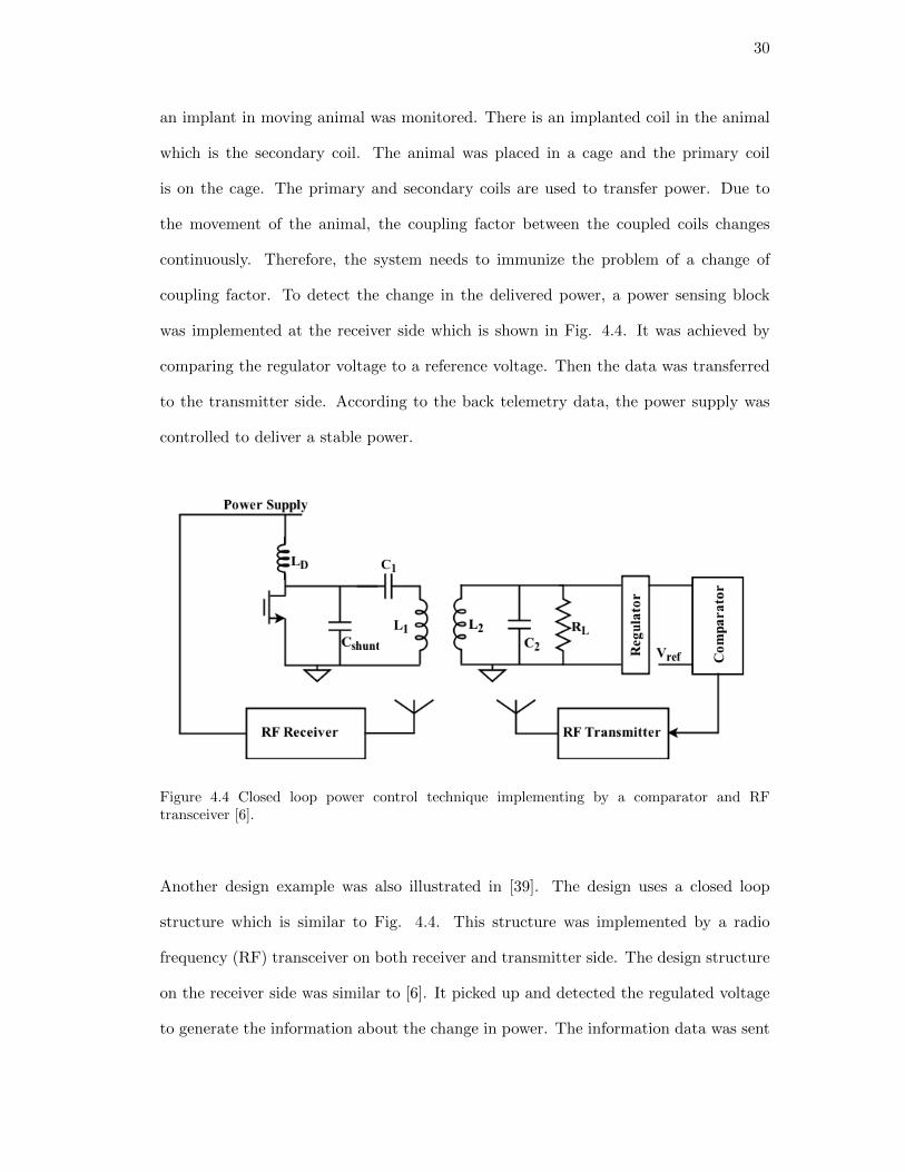
30
an implant in moving animal was monitored. There is an implanted coil in the animal
which is the secondary coil. The animal was placed in a cage and the primary coil
is on the cage. The primary and secondary coils are used to transfer power. Due to
the movement of the animal, the coupling factor between the coupled coils changes
continuously. Therefore, the system needs to immunize the problem of a change of
coupling factor. To detect the change in the delivered power, a power sensing block
was implemented at the receiver side which is shown in Fig. 4.4. It was achieved by
comparing the regulator voltage to a reference voltage. Then the data was transferred
to the transmitter side. According to the back telemetry data, the power supply was
controlled to deliver a stable power.
Figure 4.4 Closed loop power control technique implementing by a comparator and RFtransceiver [6].
Another design example was also illustrated in [39]. The design uses a closed loop
structure which is similar to Fig. 4.4. This structure was implemented by a radio
frequency (RF) transceiver on both receiver and transmitter side. The design structure
on the receiver side was similar to [6]. It picked up and detected the regulated voltage
to generate the information about the change in power. The information data was sent

31
to the external side via the RF transceiver. Based on the received data, the power
supply was changed accordingly. This system generated 10-30.2 dBm power with a
high efficiency of around 71.5 %. In the next section, the misalignment issue can also
be mitigated by using the off-the-shelf microcontroller.
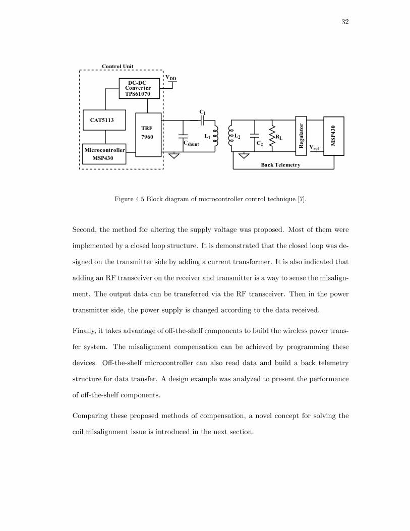
4.3 Microcontroller control methods
[7] describes to use off-the-shelf components to build wireless power transfer system.
It is a closed loop structure for biomedical implants. Several off-the-shelf components
were included in this system, such as an RFID Transceiver, a DC-DC converter and a
microcontroller. The system which is shown in Fig. 4.5 was operating at 13.65 MHz,
generating a stable 11.2 mW output power to the load via a large range. To detect the
variation of receiver power, microcontrller (MSP430) was connected to the regulator. It
is also used to detect the regulated voltage and control the back telemetry block in the
receiver to send the data. The control unit was built to alter the supply voltage of the
RFID transceiver (TRF 7960). It was designed by only using off-the-shelf components:
microcontroller (MSP 430), digital potentiometer (CAT5113) and DC-DC converter
(TPS 61070). Similar to [38], mathematical model of the system was also presented for
analyzing the stability. By changing the transfer power range from 0.5 to 2 cm, the
off-the-shelf components system can still deliver constant power at 13.65 MHz.
4.4 Conclusion
In this Chapter, different misalignment compensation methods were reviewed in de-
tail.
First, by controlling the gate drive signal of the system, the working frequency and the
duty cycle of the control signal can be altered to mitigate the misalignment effect.
32
Figure 4.5 Block diagram of microcontroller control technique [7].
Second, the method for altering the supply voltage was proposed. Most of them were
implemented by a closed loop structure. It is demonstrated that the closed loop was de-
signed on the transmitter side by adding a current transformer. It is also indicated that
adding an RF transceiver on the receiver and transmitter is a way to sense the misalign-
ment. The output data can be transferred via the RF transceiver. Then in the power
transmitter side, the power supply is changed according to the data received.
Finally, it takes advantage of off-the-shelf components to build the wireless power trans-
fer system. The misalignment compensation can be achieved by programming these
devices. Off-the-shelf microcontroller can also read data and build a back telemetry
structure for data transfer. A design example was analyzed to present the performance
of off-the-shelf components.
Comparing these proposed methods of compensation, a novel concept for solving the
coil misalignment issue is introduced in the next section.

33
Chapter 5
Proposed Concept for Coils Misalignment Compensation
The misalignment between the primary and secondary coils could naturally occur as a
result of body movement or changes in the biological environment. An immediate effect
of coil misalignment is the reduction in the power delivered to the load. In this section,
we present a design concept that could be implemented on the transmitter side, to
mitigate this effect while keeping the driver to work at its optimum operating condition.
Specifically, we will demonstrate analytically and through simulations, that tuning the
shunt capacitor and the supply voltage at the transmitter side could be a promising
approach to compensate the performance degradation induced by coil misalignment in
WPT links.
Figure 5.1 Adopted circuit model for wireless power transfer system.

34
5.1 Circuit Theory Analysis
The circuit of the adopted wireless power system is shown in Fig. 5.1. It is a two-coil
based resonance structure. The primary coil Lt and capacitor Ct form the transmitter
resonator. Rt is modeled as the parasitic resistance of the primary coil which cannot
be ignored [40]. As for the receiver side, the receiver coil is modeled as Lr, receiving
the transmitted power. The coil Lr and the capacitor Cr form the resonator in the
receiver side. The resistor Rr is used to model the parasitic resistor of Lr. The load
resistance is modeled as resistor RL. In this section, first, the receiver circuit is analyzed.
The voltage across the load is computed. Second, the reflected impedance theory is
introduced. At last, the working condition of the class E amplifier is discussed to
generate the proposed compensation approach.
5.1.1 Receiver circuit
The power transfer is based on the two coupled coils as shown in Fig. 5.2. A time
variant current it goes through the transmitter coil Lt. This current generates a time
variant magnetic field. Part of the magnetic field is picked up by the second coil Lr.
Due to the mutual coupling between these two coils, the time variant magnetic field in
the receiver coil, Lr, produces an induced voltage. This voltage will be the source at
the receiver. The induced voltage is given as:
Vind(ωt) = Mrtdit(ωt)
dωt. (5.1)
Here, Mrt is the mutual inductance between the transmitter coil Lt and the receiver
coil Lr. ω is the operational angular frequency. The Mrt can be expressed as:
Mrt = k√LtLr, (5.2)

35
Figure 5.2 Illustration of magnetic coupling working theory.
where k is the coupling factor of the two coils. The induced voltage could be modeled
at the receiver side as shown in Fig. 5.3.
At the receiver circuit, the voltage across the load RL can be computed. The capacitor
Cr is paralleled with the load RL. By using the voltage divider theory, the load voltage
can be computed as:
Vload = Vind|Zload(ω)||Ztotal(ω)|
, (5.3)
where Zload is the total load impedance, Ztotal is the total impedance of the receiver.
They can be computed as:
|Zload| = |XCr//RL| =RL√
1 + (ωRLCr)2, (5.4)
Ztotal = Rreal + jXima. (5.5)
Rreal and Xima are the real and imaginary parts of Ztoal respectively. They are ex-
pressed as:
Rreal =RL
1 +√ωRLCr
+Rr, (5.6)
Xima =ω(Lr − CrR2
L)
1 + (ωRLCr)2. (5.7)

36
Figure 5.3 The circuit diagram of WPT receiver.
Normally, the current goes into the transmitter is a sine waveform. Therefore, the
induced voltage Vind is also a sine waveform. The power P received by the load can be
expressed as:
P =V 2loadpeak
2RL. (5.8)
In this case, the load resistance RL is fixed. The factor to change the received power
is the peak voltage of the load Vloadpeak . To derive this parameter, the peak value of
induced voltage needs to be computed. It is expressed as:
Vindpeak = MrtIm = k√LrLtIm, (5.9)
where Im is the value of peak current of the transmitter current it. Therefore, the load
peak voltage can be derived:
Vloadpeak = k√LrLtIm
|Zload(ω)||Ztotal(ω)|
. (5.10)
One of the design goals is to ensure that the load receives enough stable power. It
means that the peak voltage of the load needs to be stable. From (5.10), it can be seen
that the peak voltage of the load is highly related to the coupling factor. Under the

37
Figure 5.4 Equivalent circuit seen at the transmitter employing reflected impedance theory.
condition of misalignment, the coupling factor is changed resulting in a variable peak
voltage of the load which is supposed to be stable in our design.
5.1.2 Reflected impedance theory
Reflected impedance theory is widely used in most wireless power transfer structures.
A detailed analysis of this theory was presented in [41]. This theory helps the designer
to analyze the wireless power transfer structure easily.
Employing the reflected impedance theory, the equivalent circuit at the transmitter
side is shown in Fig. 5.4. The resonant capacitor Ct and the parasitic resistors Rt are
kept the same as shown in Fig. 5.4. The transmitter coil is divided into two parts,
one is the magnetizing inductor Lmag and the other is the leakage inductor Lleak. The
reflected components are Rref and Cref paralleled with the leakage inductor Lleak. To
compute the expressions of these reflected components, the receiver circuit also needs
to be simplified. The simplified receiver circuit is shown in Fig. 5.5. The parasitic
impedance of the receiver coil Rr is converted to an equivalent resistor Req paralleled
38
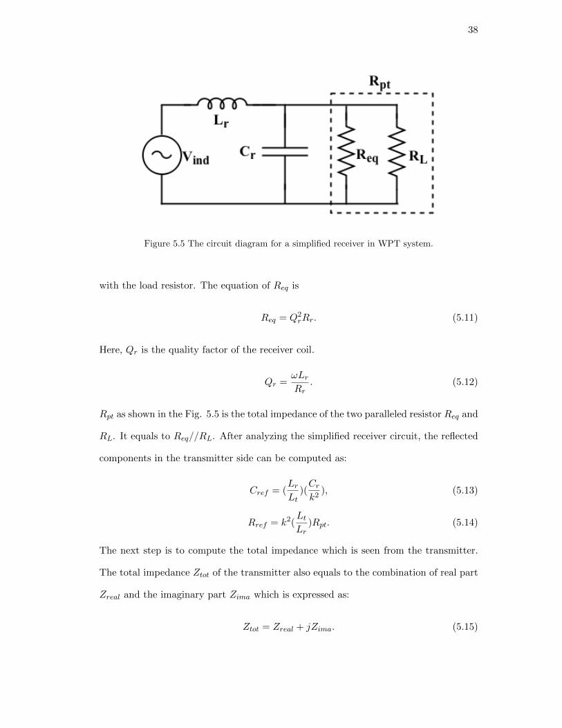
Figure 5.5 The circuit diagram for a simplified receiver in WPT system.
with the load resistor. The equation of Req is
Req = Q2rRr. (5.11)
Here, Qr is the quality factor of the receiver coil.
Qr =ωLrRr
. (5.12)
Rpt as shown in the Fig. 5.5 is the total impedance of the two paralleled resistor Req and
RL. It equals to Req//RL. After analyzing the simplified receiver circuit, the reflected
components in the transmitter side can be computed as:
Cref = (LrLt
)(Crk2
), (5.13)
Rref = k2(LtLr
)Rpt. (5.14)
The next step is to compute the total impedance which is seen from the transmitter.
The total impedance Ztot of the transmitter also equals to the combination of real part
Zreal and the imaginary part Zima which is expressed as:
Ztot = Zreal + jZima. (5.15)

39
Figure 5.6 Circuit diagram of a basic class E power amplifier.
Then, the real and imaginary parts of Ztot are computed.
Zreal(ω, k) = Rt +ω2k4L2
tRref(Rref − ω2Rrefk2L
2tCref )2 + (ωk2Lt)2
, (5.16)
Zima(ω, k) =ωk2LtRref (Rref − ω2Rrefk
2LtCref )
(Rref − ω2Rrefk2LtCref )2 + (ωk2Lt)2
+ ω((1− k2)Lt + Ct).
(5.17)
The electrical components in these equations (5.13), (5.15), (5.16) and (5.17) are fixed.
The impedance value can be changed according to the angular frequency ω and the
coupling factor k. Under the condition of misalignment, these impedance values are
impacted due to the change in the coupling factor. To understand the misalignment in
wireless power transfer system, a class E power amplifier needs to be studied. In the
next section, the analysis of class E power amplifier is performed [42].

40
5.1.3 Class E power amplifier
To drive the primary coil, a DC to AC converter is utilized. Among different kinds of
power amplifier that meet the basic requirement of the WPT system (class F, class J and
class E), class E power amplifier is selected as the main driver circuit of the primary coil
because it offers the largest power transfer efficiency [43]. By achieving the zero-voltage
switching (ZVS) and zero-voltage derivative switching (ZVDS) conditions, traditionally,
the power efficiency of the class E amplifier is 100 %.
The basic circuit structure of class E power amplifier is shown in Fig. 5.6. The ON
and OFF states of the transistor are controlled by a pulse signal. When the transistor
is turned on, it will short the shunt capacitor C. When the transistor is turned off, all
of the power will go through the load of power amplifier. If the working condition of
the class E power amplifier is ZVS and ZVDS, there is no power loss on the transistor.
All of the power which comes from the power supply is going to deliver to the load. In
biomedical implants, it is highly desirable to get the maximum power transfer efficiency.
Therefore, the class E power amplifier is selected as the driver.
By implementing the class E power amplifier in the wireless power transfer system, a
detailed analysis needs to be performed to generate the compensation results. Before
going into the detail, some assumptions are made:
1) The MOSFET transistor has no turn on and turn off resistance.
2) The duty cycle of the pulse signal generator is set to 50 %.
3) The quality factor of the load is high enough, such that the transmitter current can
be seen as a pure sine waveform:
it(ωt) = Imsin(ωt+ φ). (5.18)
If the turn on and off resistance of the transistor are included, then some power is lost

41
due to the MOSFET transistor.
By applying KCL at the drain node of MOSFET, the relationship of the current iLD,
iDS , iC , it is established.
iLD(ωt) = iDS(ωt) + iC(ωt) + it(ωt). (5.19)
Here, iLDis the current from the power supply. iDS is the drain current of the MOSFET,
iC represents the current passing through the shunt capacitor Cshunt and it is the
transmitter current which goes through the primary coil. The KVL is also applied at
the drain node. Voltage related equation is also derived as:
VDD − vDS(ωt) = vLD= ωLD
diLD(ωt)
dωt. (5.20)
Here, VDD is the supply voltage, vDS is the drain voltage across the transistor and vLD
is the voltage across the drain inductor.
To derive the analytical expressions for the transient behavior of vDS(ωt), two scenarios
are considered depending on the region of operation of the MOSFET switch, .
i) When the MOSFET is completely on (0 ≤ ωt < π). In this case, the shunt capacitor
is shorted. Therefore, the drain voltage of the MOSFET, vDS(ωt), is 0, and the shunt
capacitor current, iC(ωt), also equals to 0. These two situations can be applied to (5.19)
and (5.20), resulting in two new equations:
iLD(ωt) = iDS(ωt) + it(ωt) = iDS(ωt) + Imsin(ωt+ φ), (5.21)
VDD = vLD= ωLD
diLD(ωt)
dωt. (5.22)
Using (5.22), the drain inductor current iLDcan be derived:
iLD(ωt) =
1
ωLD
∫ ωt
0VDDdωt+ iLD
(0) = (VDDωLD
)ωt+ iLD(0). (5.23)
When ωt=0, the initial state of drain inductor current is obtained:
iLD(0) = Imsin(φ). (5.24)

42
Accordingly, (5.23) can be rewritten as:
iLD(ωt) = (
VDDωLD
)ωt+ Imsin(φ). (5.25)
ii) When the MOSFET is completely off (π ≤ ωt < 2π). In this case, the MOSFET is
modeled as an open circuit. Therefore,
iDS(ωt) = 0, (5.26)
vDS(ωt) = vC(ωt). (5.27)
Under these situations, (5.19) and (5.20) can be derived as:
iLD(ωt) = iC(ωt) + it(ωt) = iC(ωt) + Imsin(ωt+ φ), (5.28)
VDD − vC(ωt) = vLD= ωLD
diLD(ωt)
dωt. (5.29)
The current and voltage of the shunt capacitor, Cshunt should satisfy
iC(ωt) = ωCshuntdvC(ωt)
dωt. (5.30)
vc(ωt) in (5.30) can be replaced by using (5.29). Therefore, the equation for iC(ωt) can
be expressed as:
iC(ωt) = ω2CshuntLDd2iLD
(ωt)
dωt2. (5.31)
Using KCL which is expressed in (5.19), the inductor current can be derived :
iLD(ωt) = ω2CshuntLD
d2iLD(ωt)
dωt2− Imsin(ωt+ φ). (5.32)
(5.32) is a linear second order differential equation with respect to iLD(ωt). It can be
solved as:
iLD(ωt)
Im= Asin(αωt) +Bcos(αωt) +
α2sin(ωt+ φ)
α2 − 1, (5.33)
where
α =1
ω√LDCshunt
. (5.34)

43
Here, A and B are the two factors which are determined by the boundary conditions
of (5.32).
During the transition of the transistor from the ON to the OFF state, the inductor’s
current, iLD, and the voltage across the shunt capacitor, VC , must remain continuous.
Therefore, the boundary conditions for iLDand its derivative, i
′LD
, at ωt=π can be
written as:
iLD(π+) = iLD
(π−) =VDDπ
ωLD+ Imsin(φ), (5.35)
i′LD
(π−) = i′LD
(π+) =VDDωLD
(5.36)
These boundary conditions can be applied in (5.33) to solve the factors A and B. Then
we obtain:
iLD
Im(π+) =
π
β+ sin(φ), (5.37)
and
i′LD
Im(π+) =
1
β, (5.38)
where β is defined as
β =ImLDω
VDD. (5.39)
As a result, A and B are derived as:
A =1
α2 − 1[αcos(απ)cos(φ)+(2α2−1)sin(απ)sin(φ)]+
π
βsin(απ)+
1
αβcos(απ), (5.40)
B =1
α2 − 1[−αsin(απ)cos(φ) + (2α2 − 1)cos(απ)sin(φ)] +
π
βcos(απ)− 1
αβsin(απ).
(5.41)
The voltage across the source and drain of the transistor during the OFF state can then
be obtained from (5.20) by using iLDin (5.33),
vDS(ωt) =VDD − βVDD[αAcos(αωt)− αBsin(αωt)+
α2cos(ωt+ φ)
α2 − 1]. (π ≤ ωt < 2π)
(5.42)

44
The expression of vDS(ωt) during the full period can be derived based on the above
analysis. During 0 ≤ ωt < π, the MOSFET is turned on without any resistance in-
dicating that vDS(ωt) equals to 0. In the second half, π ≤ ωt < 2π, vDS(ωt) follows
expression described in (5.42).
To maintain an optimum working condition of class E power amplifier, the ZVS and
ZVDS conditions need to be satisfied. The two conditions can be expressed by using
equations:
vDS(2π) = v′DS(2π) = 0, (5.43)
where v′DS is the derivation of vDS . The conditions should be applied to (5.42), then
two new equations are derived:
VDD − βVDD[αAcos(α2π)− αBsin(α2π) +α2
α2 − 1(cosφ)] = 0, (5.44)
and
βVDD[αAsin(α2π) + αBcos(α2π) +α2
α2 − 1(sinφ)] = 0. (5.45)
From these equations, β and φ can be derived as functions of α to satisfy both condi-
tions.
β = f(α), (5.46)
φ = u(α). (5.47)
Based on the assumptions stated earlier in the section, there are no losses on the
transistor of class E power amplifier. Therefore, the power taken from the power supply
is received by Zreal which is the real part of the transmitter resistance illustrated in the
reflected resistance section and can be expressed as:
VDDIo =1
2I2mZreal(ω, k). (5.48)
where Io is the DC supply current and k is the coupling factor. The current Io is derived
as the average of the total current going through the supply voltage during the whole

45
period,
Io =1
2π
∫ 2π
0iLD
(ωt)dωt. (5.49)
By simplifying the right side of (5.49), Io can be obtained:
Io =Im2
(π
2β− 2
πcos(φ) + sin(φ)). (5.50)
Replacing (5.34), (5.39) and (5.50) in (5.49) one can obtain:
α2βZreal(ω, k)Cshunt − (π
2β− 2
πcos(φ) + sin(φ)) = 0. (5.51)
To satisfy the ZVS and ZVDS conditions, parameters β and φ can be derived as func-
tions of α. By replacing (5.46), (5.47) in (5.51) and knowing the α depends on the ω,
it can be seen that variations in ω or k could impact the equality in (5.51).
All of the above equations concerning the class E power amplifier are derived under the
optimum working conditions. In the case of misalignment, the coupling factor is going
to be changed. This variation will alter the working condition of the class E power
amplifier, meaning (5.51) cannot hold its equality. Additionally, based on the circuit
analysis, the power delivered to the load is also changed. Thus, an approach needs to
be developed to solve these problems in WPT system under coils misalignment. The
proposed compensation approach is introduced in the next section.
5.2 Proposed Compensation Concept
5.2.1 Illustration of Misalignment Compensation Concept
The main goal of the proposed compensation concept is to ensure that the class E
amplifier works at ZVS and ZVDS operating conditions, and Vloadpeak , as defined in
(5.10), remains constant. These key parameters could be easily changed because of the
coupling factor due to the misalignment.

46
To maintain the optimum operational condition of the class E amplifier, (5.44), (5.45)
and (5.48) need to be satisfied. (5.51) is the combination of these equations. If the
coupling factor is altered due to the misalignment, (5.51) cannot hold its equality. It
means that the operation of class E amplifier is not optimum and hence a new α needs
to be derived. To hold the equality of (5.44) and (5.45), β and φ can be expressed using
α. The expressions of β and α are applied in (5.51). According to (5.34), α depends
on the electrical components of the circuits and the angular frequency ω. By keeping ω
and drain inductor LD constant, the parameter Cshunt can be altered at the transmitter
side to obtain the required new α, corresponding to the new β and φ to ensure that the
class E power amplifier works at its optimum operating condition.
In this situation, the optimum operating condition of class E power amplifier is achieved.
But the power delivered to the load could still vary. According to (5.39), the new value
of β can force Im to change, if VDD, ω and LD are kept constant. Therefore, in (5.10),
the coupling factor k and the peak transmitter current Im both change, resulting in a
variation in the peak voltage at the load, Vloadpeak . However, if the change in Im can
be controlled, it will compensate for the variation in k, generating a stable load peak
voltage. This can be achieved by changing the supply voltage VDD in the transmitter
and fixing the drain inductor. In (5.39), once β and LD are fixed, accordingly the Im
can be changed to a desired value for compensation by altering the supply voltage to a
specific number.
To summarize, if k changes due to misalignment, altering the shunt capacitor and
the supply voltage at the transmitter side could be a potential solution to ensure the
WPT system continues to deliver a stable power to the load even in the presence of
misalignment.

47
5.2.2 Simulation Results
To validate the proposed concept for compensation concept, simulations were performed
using MATLAB (based on the analytical expression) and Cadence (based on circuit
simulation). The component values used for circuit simulation were taken from [40].
The duty cycle of the driver signal applied to the gate of the transistor was set to
50%.
The coupling factor, k, and the load peak voltage value in the absence of misalignment,
were set to 0.3 and 3.5 V, respectively. To model different misalignment scenarios, the
value of the coupling factor, k, was manually changed. For each k, the shunt capacitor
and the supply voltage required for achieving an optimum working condition of the class
E amplifier and to maintain the peak voltage value at 3.5 V were obtained analytically
using MATLAB. The values of these design parameters can be obtained by computing
the equations which are shown in class E power amplifier analysis section.
To get simulation results, the circuit schematic shown in Fig. 5.1 is built in Cadence.
The coupling factor of the two coupled coils in this circuit is changed, and the shunt
capacitor is also changed, accordingly. By analyzing the waveform of vDS , the proper
value of the shunt capacitor Cshunt is recorded to deliver a ZVS and ZVDS drain voltage
waveform. After that, the supply voltage VDD is altered to get the stable load peak
voltage by seeing the load voltage Vload waveform. The proper supply voltage values
are also recorded.
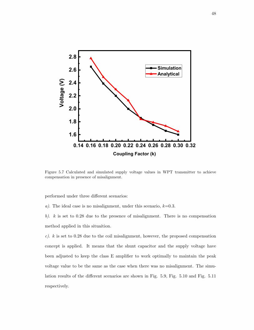
Fig. 5.7 and Fig. 5.8 show required supply voltage values and shunt capacitor values
for compensating the negative effect of the misalignment, obtained analytically and
through simulation, respectively.
Transient simulation is also performed to validate the proposed concept. The transient
simulation shows the load voltage and drain voltage, respectively. The simulation is
48
0.14 0.16 0.18 0.20 0.22 0.24 0.26 0.28 0.30 0.32
1.6
1.8
2.0
2.2
2.4
2.6
2.8Vo
ltage
(V)
Coupling Factor (k)
Simulation Analytical
Figure 5.7 Calculated and simulated supply voltage values in WPT transmitter to achievecompensation in presence of misalignment.
performed under three different scenarios:
a). The ideal case is no misalignment, under this scenario, k=0.3.
b). k is set to 0.28 due to the presence of misalignment. There is no compensation
method applied in this situaition.
c). k is set to 0.28 due to the coil misalignment, however, the proposed compensation
concept is applied. It means that the shunt capacitor and the supply voltage have
been adjusted to keep the class E amplifier to work optimally to maintain the peak
voltage value to be the same as the case when there was no misalignment. The simu-
lation results of the different scenarios are shown in Fig. 5.9, Fig. 5.10 and Fig. 5.11
respectively.

49
0.18 0.20 0.22 0.24 0.26 0.28 0.300.1
0.2
0.3
0.4
0.5
0.6
0.7
0.8
Cap
acita
nce
(nF)
Coupling Factor (k)
Simulation Analytical
Figure 5.8 Calculated and simulated shunt capacitor values in WPT transmitter to achievecompensation in presence of misalignment.
The ideal situation is shown in Fig. 5.9, it illustrates the class E power amplifier
is working at its optimum situation. Under the condition of misalignment, which is
simulated by reducing the coupling factor to 0.28, Fig. 5.10 shows a non-optimum
operating condition for class E power amplifier where the load peak voltage is also
accordingly reduced. By tuning the shunt capacitor and supply voltage, the working
condition of class E power amplifier is restored and the load peak voltage reaches to
the original value. These results verify that our proposed compensation concept can
mitigate the negative effects of coils misalignment.

50
9.5 9.6 9.7 9.8 9.9 10.0
0
1
2
3
4
5
6
9.5 9.6 9.7 9.8 9.9 10.0
-4
-3
-2
-1
0
1
2
3
4
5
Volta
ge (V
)
Time (s)Vo
ltage
(V)
Time (s)
3.5 V
Figure 5.9 Simulated waveforms on the drivers drain voltage, Vds, and on the loads peak voltageunder optimum operation condition at k=0.3.
9.5 9.6 9.7 9.8 9.9 10.0
-1
0
1
2
3
4
5
6
9.5 9.6 9.7 9.8 9.9 10.0-4
-3
-2
-1
0
1
2
3
4
5
Volta
ge (V
)
Time (s)
nonoptimum operation
Volta
ge (V
)
Time (s)
3.38 V
Figure 5.10 Simulated waveforms on the drivers drain voltage, Vds, and on the loads peak voltageunder the presence of misalignment at k=0.28, no compensation.

51
9.5 9.6 9.7 9.8 9.9 10.0
0
1
2
3
4
5
6
9.5 9.6 9.7 9.8 9.9 10.0
-4
-3
-2
-1
0
1
2
3
4
5
Volta
ge (V
)
Time (s)Vo
ltage
(V)
Time (s)
3.5 V
Figure 5.11 Simulated waveforms on the drivers drain voltage, Vds, and on the loads peak voltageunder the presence of misalignment at k=0.28, with applying compensation.
5.2.3 Advantages of the proposed misalignment compensation design
There are three main merits of this proposed method.
First, several proposed techniques use tuning of the working frequency for compensation
[3] [4]. However, this method has its disadvantage. According to [5], the disadvantage is
that changing the working frequency is going to alter the power transfer efficiency of the
coupled coils. It is undesirable to change the power transfer efficiency of the coupled
coils while solving the misalignment problems. Therefore, to overcome the changing
power transfer efficiency disadvantage, in our proposed method the working frequency
remains the same to ensure a stable power transfer efficiency.
Second, the misalignment will not only change the power delivered to the load, but
the working condition of the class E power amplifier is also altered. Most of previous

52
design did not address this issue. In our design method, the class E power amplifier can
restore its optimum working condition even under the misalignment situations. Also
the power delivered to the load can be maintained a constant.
Third, to realize the previous proposed techniques, some additional circuitry is re-
quired. This will increase the design difficulty of the system. For example, in [3], the
drain inductor was changed to address for misalignment compensation. To change the
inductor, an extra component was added in the transmitter increasing the complexity
of the system. In our proposed method, by designing an integrated system, the shunt
capacitor can be tuned by using a varactor, for example. There is no need for extra
components hence reducing the design difficulty.
5.3 Conclusion
In this chapter, a compensation concept for mitigating the negative effects of coil mis-
alignment in wireless power transfer links used in biomedical implants was presented.
The circuit theory for the operation of wireless power transfer system was discussed in
detail. The receiver circuit was analyzed for deriving the expression of the peak voltage.
Then, the reflected impedance theory was used for obtaining the operating condition of
the class E power amplifier. Based on the derived equations, a compensation method,
by altering the shunt capacitor and supply voltage, was proposed. Simulation results
based on the proposed compensation concept were also presented verifying the valida-
tion of proposed method.

53
Chapter 6
Conclusions
Wireless power transfer (WPT) technique finds applications in variety of systems, es-
pecially in biomedical implants. For biomedical implants, delivering a constant power
is highly desired and the power transfer efficiency should be maximized [42]. One of
the issue which adversely affects the power transmission is the misalignment between
the coils forming [30]. To mitigate this effect, a design compensation concept, which
can achieve a stable load power delivery and maintain the driver circuit working in its
optimum condition without changing the power transfer efficiency of the inductive link
was proposed.
The contributions of this thesis are listed as follows:
1 . An overview of wireless power transfer technique was presented. Based on the
distance d of wireless power transfer and the power transfer wavelength λ, three
categories were demonstrated: near field (d < λ/2π), mid field (λ/2π < d < λ/π)
and far field (d > λ/π). If the power needs transferring via a large distance,
the microwave or photo-electricity techniques are adopted. To transfer power in
centimeters range, such as in biomedical implants, the magnetic coupling method
in generally selected. If the power transfer distance is in mid field range, the
combination of inductive and radiative models is utilized.
2 . Different structures for the magnetic coupling, classified as resonant coupling

54
and inductive coupling in biomedical implants, were introduced [5]. The resonance
based wireless power transfer structures have been used because it can achieve
higher power transfer efficiency than inductive coupling [5]. Based on the number
of the coils, two-coil, three-coil and four-coil based resonant wireless power transfer
systems were demonstrated. The models of these structures were mathematically
analyzed using math equations. The design parameters, such as the power transfer
efficiency, were computed.
3 . The issue of the coil misalignment was reviewed. Two different scenarios of
the misalignment, the angular and position displacement, were presented. The
mutual inductance of the misalignment coils was computed. It was shown that
once the misalignment happens, the mutual inductance and the coupling factor k
are highly impacted.
4 . The prior work regarding the misalignment compensation in wireless power
transfer was reviewed. First, it was proposed that tuning the operational fre-
quency is a method to compensate the negative effect induced by the misalignment
of primary and secondary coils. Additionally, the power supply in the transmitter
side has been proved to be another method to do the compensation. To realize the
method of altering power supply, radio frequency (RF) transceiver has been built
in the receiver and transmitter for transferring data. According to these trans-
ferred data, the proper amount of supply voltage for tuning can be obtained.
Finally, the off-the-shelf components are used to built the wireless power transfer
system. By programming these products, the misalignment issues can be solved.
5 . The presented misalignment compensation design concept was presented. The
receiver circuit was analyzed for computing the power received by the load. The
reflected impedance theory and the driver circuit were discussed. Based on these

55
theory, it was shown that by tuning the shunt capacitor and the supply voltage,
the misalignment can be compensated, achieving the optimum working condition
of the class E power amplifier and maintaining a constant power delivery to the
load. Simulation results were performed to verify valitity of the proposed the
concept.

56
Bibliography
[1] Mehdi Kiani and Maysam Ghovanloo. Near-field wireless power and data trans-
mission to implantable neuroprosthetic devices. In Neural Computation, Neural
Devices, and Neural Prosthesis, pages 189–215. Springer, 2014.
[2] Shawon Senjuti. Design and optimization of efficient wireless power transfer links
for implantable biotelemetry systems (thesis format: Monograph), 2013.
[3] Samer Aldhaher, PC-K Luk, and James F Whidborne. Electronic tuning of mis-
aligned coils in wireless power transfer systems. Power Electronics, IEEE Trans-
actions on, 29(11):5975–5982, 2014.
[4] Philip R Troyk and Martin AK Schwan. Closed-loop class e transcutaneous power
and data link for microimplants. Biomedical Engineering, IEEE Transactions on,
39(6):589–599, 1992.
[5] Rajiv Jay and Samuel Palermo. Resonant coupling analysis for a two-coil wireless
power transfer system. In Circuits and Systems Conference (DCAS), 2014 IEEE
Dallas, pages 1–4, 2014.
[6] Nattapon Chaimanonart, Mark D Zimmerman, and Darrin J Young. Adaptive rf
power control for wireless implantable bio-sensing network to monitor untethered
laboratory animal real-time biological signals. In Sensors, 2008 IEEE, pages 1241–
1244, 2008.
[7] Mehdi Kiani and Maysam Ghovanloo. An RFID-based closed-loop wireless power

57
transmission system for biomedical applications. Circuits and Systems II: Express
Briefs, IEEE Transactions on, 57(4):260–264, 2010.
[8] Richard S Sanders and Michel T Lee. Implantable pacemakers. Proceedings of the
IEEE, 84(3):480–486, 1996.
[9] Francis A Spelman. The past, present, and future of cochlear prostheses. Engi-
neering in Medicine and Biology Magazine, IEEE, 18(3):27–33, 1999.
[10] Seung Bae Lee, Byunghun Lee, Benoit Gosselin, and Maysam Ghovanloo. A dual
slope charge sampling analog front-end for a wireless neural recording system. In
Engineering in Medicine and Biology Society (EMBC), 2014 36th Annual Inter-
national Conference of the IEEE, pages 3134–3137, 2014.
[11] R-F Xue, K-W Cheng, and Minkyu Je. High-efficiency wireless power transfer
for biomedical implants by optimal resonant load transformation. Circuits and
Systems I: Regular Papers, IEEE Transactions on, 60(4):867–874, 2013.
[12] Zhen Ning Low, Raul Andres Chinga, Ryan Tseng, and Jenshan Lin. Design and
test of a high-power high-efficiency loosely coupled planar wireless power transfer
system. Industrial Electronics, IEEE Transactions on, 56(5):1801–1812, 2009.
[13] Anil Kumar RamRakhyani, Shahriar Mirabbasi, and Mu Chiao. Design and opti-
mization of resonance-based efficient wireless power delivery systems for biomedi-
cal implants. Biomedical Circuits and Systems, IEEE Transactions on, 5(1):48–63,
2011.
[14] Michael P Theodoridis. Effective capacitive power transfer. Power Electronics,
IEEE Transactions on, 27(12):4906–4913, 2012.
[15] Amir M Sodagar and Parviz Amiri. Capacitive coupling for power and data teleme-
try to implantable biomedical microsystems. In Neural Engineering, 2009. NER’09.

58
4th International IEEE/EMBS Conference on, pages 411–414, 2009.
[16] H Zheng, K Tnay, N Alami, and AP Hu. Contactless power couplers for respiratory
devices. In Mechatronics and Embedded Systems and Applications (MESA), 2010
IEEE/ASME International Conference on, pages 155–160, 2010.
[17] Aiguo Patrick Hu, Chao Liu, and Hao Leo Li. A novel contactless battery charging
system for soccer playing robot. In Mechatronics and Machine Vision in Practice,
2008. M2VIP 2008. 15th International Conference on, pages 646–650. IEEE, 2008.
[18] Mitchell Kline, Igor Izyumin, Bernhard Boser, and Seth Sanders. Capacitive power
transfer for contactless charging. In Applied Power Electronics Conference and
Exposition (APEC), 2011 Twenty-Sixth Annual IEEE, pages 1398–1404, 2011.
[19] Byung Woo Yoon. Power delivery circuit for scalable claytronics. MSc Report,
Carnegie Mellon University, Department of Electrical and Computer Engineering,
2007.
[20] Farzad Asgarian and Amir M Sodagar. Wireless Telemetry for Implantable
Biomedical Microsystems. INTECH Open Access Publisher, 2011.
[21] Mustafa Emre Karagozler, Jason D Campbell, Gary K Fedder, Seth Copen Gold-
stein, Michael Philetus Weller, and Byung Woo Yoon. Electrostatic latching for
inter-module adhesion, power transfer, and communication in modular robots. In
Intelligent Robots and Systems, 2007. IROS 2007. IEEE/RSJ International Con-
ference on, pages 2779–2786, 2007.
[22] Bert Lenaerts and Robert Puers. Omnidirectional inductive powering for biomed-
ical implants. Springer, 2009.
[23] Yiming Zhang, Zhengming Zhao, and Kainan Chen. Frequency decrease analysis

59
of resonant wireless power transfer. Power Electronics, IEEE Transactions on, 29
(3):1058–1063, 2014.
[24] Nikola Tesla. The transmission of electrical energy without wires as a means for
furthering peace. Electrical World and Engineer. Jan, 7:21, 1905.
[25] William C Brown. The technology and application of free-space power transmission
by microwave beam. Proceedings of the IEEE, 62(1):11–25, 1974.
[26] David Smith. Wireless power spells end for cables. The Observer (London), 2009.
[27] John S Ho, Sanghoek Kim, and Ada SY Poon. Midfield wireless powering for
implantable systems. Proceedings of the IEEE, 101(6):1369–1378, 2013.
[28] Ada SY Poon, Stephen O’Driscoll, and Teresa H Meng. Optimal frequency for
wireless power transmission into dispersive tissue. Antennas and Propagation,
IEEE Transactions on, 58(5):1739–1750, 2010.
[29] Mehdi Kiani, Uei-Ming Jow, and Maysam Ghovanloo. Design and optimization of
a 3-coil inductive link for efficient wireless power transmission. Biomedical Circuits
and Systems, IEEE Transactions on, 5(6):579–591, 2011.
[30] Kyriaki Fotopoulou and Brian W Flynn. Wireless power transfer in loosely coupled
links: Coil misalignment model. Magnetics, IEEE Transactions on, 47(2):416–430,
2011.
[31] Frederick Warren Grover. Inductance calculations: working formulas and tables.
Courier Corporation, 1946.
[32] Chester Snow. Formulas for computing capacitance and inductance, volume 544.
US Govt. Print. Off., 1954.
[33] FC Flack, ED James, and DM Schlapp. Mutual inductance of air-cored coils: Effect

60
on design of radio-frequency coupled implants. Medical and biological engineering,
9(2):79–85, 1971.
[34] Erwin S Hochmair. System optimization for improved accuracy in transcutaneous
signal and power transmission. Biomedical Engineering, IEEE Transactions on,
(2):177–186, 1984.
[35] Slobodan I Babic and Cevdet Akyel. Calculating mutual inductance between cir-
cular coils with inclined axes in air. Magnetics, IEEE Transactions on, 44(7):
1743–1750, 2008.
[36] Milton Abramowitz, Irene A Stegun, et al. Handbook of mathematical functions,
volume 1. Dover New York, 1972.
[37] Izrael Solomonovich Gradshtejn and Iosif Moiseevich Ryzhik. Table of integrals,
series and products. Academic Press, 1965.
[38] Guoxing Wang, Wentai Liu, Mohanasankar Sivaprakasam, and Gurhan Alper
Kendir. Design and analysis of an adaptive transcutaneous power telemetry for
biomedical implants. Circuits and Systems I: Regular Papers, IEEE Transactions
on, 52(10):2109–2117, 2005.
[39] P Si, AP Hu, JW Hsu, M Chiang, Y Wang, S Malpas, and D Budgett. Wireless
power supply for implantable biomedical device based on primary input voltage
regulation. In Industrial Electronics and Applications, 2007. ICIEA 2007. 2nd
IEEE Conference on, pages 235–239. IEEE, 2007.
[40] Gurhan Alper Kendir, Wentai Liu, Guoxing Wang, Mohanasankar Sivaprakasam,
Rizwan Bashirullah, Mark S Humayun, and James D Weiland. An optimal design
methodology for inductive power link with class-e amplifier. Circuits and Systems
I: Regular Papers, IEEE Transactions on, 52(5):857–866, 2005.

61
[41] Mehdi Kiani and Maysam Ghovanloo. The circuit theory behind coupled-mode
magnetic resonance-based wireless power transmission. Circuits and Systems I:
Regular Papers, IEEE Transactions on, 59(9):2065–2074, 2012.
[42] Fanpeng Kong, Yi Huang, and Laleh Najafizadeh. A coil misalignment compensa-
tion concept for wireless power transfer links in biomedical implants. In Wireless
Power Transfer Conference (WPTC), 2015 IEEE, pages 1–4, 2015.
[43] Seunghoon Jee, Junghwan Moon, Jungjoon Kim, Junghwan Son, and Bumman
Kim. Switching behavior of class-e power amplifier and its operation above maxi-
mum frequency. Microwave Theory and Techniques, IEEE Transactions on, 60(1):
89–98, 2012.