coaxial tip piezores istive scanning …web.stanford.edu/group/ggg/harjee-mems-2010.pdfcoaxial tip...
TRANSCRIPT
COAXIAL TIP PIEZORESISTIVE SCANNING PROBES FOR HIGH-RESOLUTION ELECTRICAL IMAGING
N. Harjee, A.G.F. Garcia, M. König, J.C. Doll, D. Goldhaber-Gordon, and B.L. Pruitt Stanford University, Stanford, CA, USA
ABSTRACT We have designed and batch fabricated silicon cantilever scanning probes integrating, for the first time, a coaxial tip to produce highly localized electric fields and a piezoresistor to measure cantilever deflection. These probes will improve the lateral resolution of scanning gate microscopy enabling the study of electron organization in semiconductor nanostructures. The full-width at half-maximum of the perturbation produced by our coaxial tip is ~3x smaller than that of conventional tips. At 300 K, the vertical displacement resolution of a 405 µm long probe is 2.4 nm in a 1 kHz bandwidth. With the ability to image topography and apply local electric fields, our probe has broad applications including electromechanical studies of cells and dopant profiling in semiconductors. INTRODUCTION Fundamentally similar to atomic force microscopy (AFM), scanning gate microscopy (SGM) is used to study electron flow and organization [1-3]. In this technique, a voltage is applied to a conductive probe that is raster-scanned across a sample. Through capacitive coupling, charge on the tip perturbs the energy landscape of the sample. The resulting change in conductance through the sample provides information about the electrons beneath the tip. Typically, SGM has been performed with commercial AFM probes that are coated with a thin layer of metal. These probes produce broad electric fields that limit lateral resolution and increase imaging complexity. In order to apply SGM to semiconductor nanostructures, there is a need for a probe that can produce a highly localized electric field perturbation. This probe must also be compatible with AFM to allow tip-sample registration. We have designed and fabricated single crystal silicon cantilever scanning probes integrating, for the first time, a coaxial tip to produce sharp, dipolar electric fields and a piezoresistor to measure cantilever deflection. Separately, coaxial tips and piezoresistors have been demonstrated for scanning near-field microscopy [4-10] and AFM [11-13]. However, this work presents the first batch microfabrication of cantilevers with both features for self-sensing scanning probe metrologies.
By combining compact, low-cost AFM with the ability to produce highly localized electric fields, our probe has many applications beyond SGM including electromechanical studies of cells, dopant/trap profiling in semiconductors and scanning electrochemical microscopy. DESIGN The mechanical properties of our probes are closely matched to those of the Veeco Piezolevers they are designed to replace. Cantilever thickness and width are fixed at 3 µm and 50 µm while length is varied from 155 µm to 405 µm yielding spring constants of 0.85-15 N/m and resonant frequencies of 25-170 kHz. Tip height is limited to ~3 µm to facilitate lithographic processing after the tips are etched. The effect of tip configuration and geometry on electric field distribution was estimated with a custom Matlab 2D Poisson solver. According to our model, the full-width at half-maximum of the perturbation produced by a coaxial tip is ~3x smaller than that of a conductive AFM tip when both are located 50 nm above a ground plane. It is essential that SGM probes be self-sensing as stray photons from the laser in conventional AFM setups can excite electrons in the samples, disturbing the measurement. Recent advances in sensitivity and noise optimization [14,15] guided the design of our piezoresistors yielding high stability and displacement resolution. FABRICATION Our scanning probes were fabricated from 4-inch (100) 1-5 Ω-cm n-type silicon-on-insulator wafers. After singeing the wafers at 150ºC and priming with hexamethyldisilazane (HMDS), global alignment marks were patterned in 1.6 µm of Shipley 3612 photoresist using a Karl Suss MA-6 mask aligner in hard contact. The marks were etched 3000 Å into the 6 µm device layer with SF6 plasma. The resist was stripped in 9:1 H2SO4:H2O2, and the wafers were oxidized at 1000ºC in a wet ambient for 40 minutes. The 3000 Å oxide was patterned into 6 µm diameter discs using 6:1 BOE (34% NH4F:7% HF:59% H2O) as a hard mask for the following tip etch. The discs were undercut with an isotropic silicon etch in SF6 plasma (150 mT, 500 W, 100 sccm SF6, 10 sccm O2) to form ~3 µm tall tip precursors. The etch was
978-1-4244-5764-9/10/$26.00 ©2010 IEEE
344

stopped when the tops of the precursors could no longer be resolved through the transparent oxide discs using an optical microscope. The discs were removed in 6:1 BOE and the tips were sharpened by wet oxidation at 950ºC for 55 min after Ravi et al. [16]. The resulting oxide was stripped in 6:1 BOE. The p-type piezoresistors at the clamped ends of the cantilevers and inner conductors of the coaxial tips were formed by ion implantation. To protect the tips and minimize channeling effects during the implant, the wafers were oxidized at 900ºC in a wet ambient for 9 minutes to grow a 250 Å screening oxide. We spun and patterned 7 µm of Shipley 220-7 photoresist as the implant mask. After hard baking the resist at 110ºC for 30 minutes, the wafers were implanted with a 6x1015 cm-2 dose of BF2 at 50 keV and 7º tilt (NuIons, San Jose, CA). Because BF2 is more massive than boron, it has a shorter implant range, enabling us to achieve the shallow implant necessary for high piezoresistor sensitivity. The resist and
damaged oxide were stripped and a 1000 Å of oxide was grown in 19 min at 950ºC in a wet ambient to form the coaxial insulator. This high temperature step also activated and diffused the implanted dopants, yielding a junction depth of 0.6 µm, verified by spreading resistance analysis (Solecon, Reno, NV). Contacts were opened in the oxide with 6:1 BOE and electrodes and the coaxial shields were formed by sputtering and patterning 1500 Å of Al + 1% Si using a combination of wet etching in AL-11 (72% H3PO4:3% C2H4O2:3% HNO3:12% H2O) and dry etching in SF6 plasma. All subsequent photoresist strips were performed in PRX-127. The cantilever geometry was defined by deep reactive ion etching (DRIE) of the remaining ~3 µm device layer with the 0.5 µm buried oxide (BOX) as an etch stop. Probe release was accomplished by backside lithography and DRIE of the ~400 µm handle layer, again stopping on the BOX. Delicate features were protected by spinning 10 µm of Shipley 220-7 photoresist on the frontside prior to backside processing. The BOX was etched in CHF3/O2 plasma. The wafers were given a final clean in PRS-1000 and annealed in forming gas (4% H2 in N2) for 2 hours at 400ºC to improve electrical contacts. To complete the coaxial structure, the shield metal at the tip apex was opened with focused ion beam (FIB) milling on an FEI Strata 235DB. Using a circular beam pattern of radius 200 nm centered on the apex and a Ga+ beam current of 10 pA, opening radii of
Figure 1. Fabrication process: (a) Isotropic Si etch to create tips (b) BF2 implant to form piezoresistor and inner conductor (c) Oxidation and contact opening (d) Metallization and patterning into electrodes and shield (e) DRIE to define cantilevers (f) Release with backside DRIE and plasma etch of BOX. Shield opened at tip apex with FIB.
Figure 2. Scanning electron micrographs of a fabricated scanning probe: (a) 1.6 mm x 3.6 mm die featuring a 3 µm thick x 50 µm wide x 255 µm long silicon cantilever with implanted BF2 piezoresistor and inner conductor, SiO2 insulator and Al electrodes and shield; a 3 µm tall coaxial tip (b) before FIB (oblique) and after FIB from (c) oblique and (d) top views. FIB opening in Al/SiO2 at tip apex is ~100 nm in radius.
Si
a
BF2 Implant AlSiO2
b
c
d
e
f
Al
p-type Si
500 nm
AlSiO2
SiO2
p-type Si500 nm
c d
Al
Al
1 !m
ba
500 !m
345

~100 nm were achieved. The fabrication process is shown in Figure 1 and a finished device is shown in Figure 2. MEASUREMENTS To characterize piezoresistor performance, we measured the vertical displacement resolution of a
405 µm long probe at 300 K and 300 mK, typical SGM temperatures. At room temperature, we placed the ~6.2 kΩ piezoresistor in a Wheatstone bridge with matched metal film resistors. The bridge was biased at 5 V and connected to two AD8221 instrumentation amplifiers in series providing a total gain of 200x. The probe was mounted in a Witec Alpha300A AFM system using a custom printed circuit board and the readout circuit was connected to an auxiliary input on the controller. Low temperature measurements were performed in a 3He cryostat. All of the resistors in the Wheatstone bridge were cooled to 300 mK. The bias on the bridge was reduced to 0.1 V to accommodate the maximum cooling power of the fridge and the gain was increased to 100,000x using two PAR-113 amplifiers in series. The probe was mounted at the end of an RHK piezoelectric scan tube attached to Attocube slip-stick nanopositioners. In both experimental setups, we obtained voltage-displacement curves by deflecting the probe with a hard sample. Displacement resolution was calculated by dividing integrated noise in the measurement bandwidth by sensitivity. The minimum detectable displacement at 300 K was 2.4 nm (1 kHz bandwidth) and at 300 mK was 12 nm (0.2 kHz bandwidth). Table 1 summarizes these results and Figure 3 provides representative plots of sensitivity and noise. To demonstrate topographic imaging with the integrated piezoresistor, we selected the auxiliary input as the control channel for z-axis feedback on the Alpha300A and scanned the probe over a test sample. Figure 4 is an image of gold electrodes on silicon dioxide taken in contact mode with a setpoint of 2 V.
Figure 4. AFM image of Au electrodes on SiO2. Z-axis height controlled by piezoresistive feedback.
Figure 3. Piezoresistor (a) sensitivity and (b) noise recorded in a 3He cryostat at 300 mK. The tip is positioned by an RHK piezoelectric scan tube attached to an Attocube slip-stick nanopositioner. Amplifier output is captured using an NI DAQ PCI card with custom software and breakout box.
Table 1. Parameters and results of vertical displacement resolution measurements for a 405 µm long cantilever.
300 K 300 mK Bridge bias 5 V 0.1 V Amplifiers AD8221 PAR-113 Total gain 200x 100,000x Sensitivity 0.23 mV/nm 1.2 mV/nm Measured ΔR/R 0.92 ppm/nm 0.48 ppm/nm Theoretical ΔR/R 1.7 ppm/nm Bandwidth 1 kHz 0.2 kHz Integrated noise 2.8 µV 0.15 µV Resolution 2.4 nm 12 nm
123.1 nm
0 nm
100 101 10210
10
10
10
10
10
Frequency (Hz)
Volta
ge n
oise
(V/H
z)
Theoretical Johnson noise:
T = 300 mKVbias = 100 mV
0 100 200 300 400
Theoretical sensitivity at 300 K:
1.2 mV/nmat 300 mKwith 105x gain
A - amplifier gainVbias - bridge biasG - piezo gauge factort - lever thicknessL - lever length
a
b
346
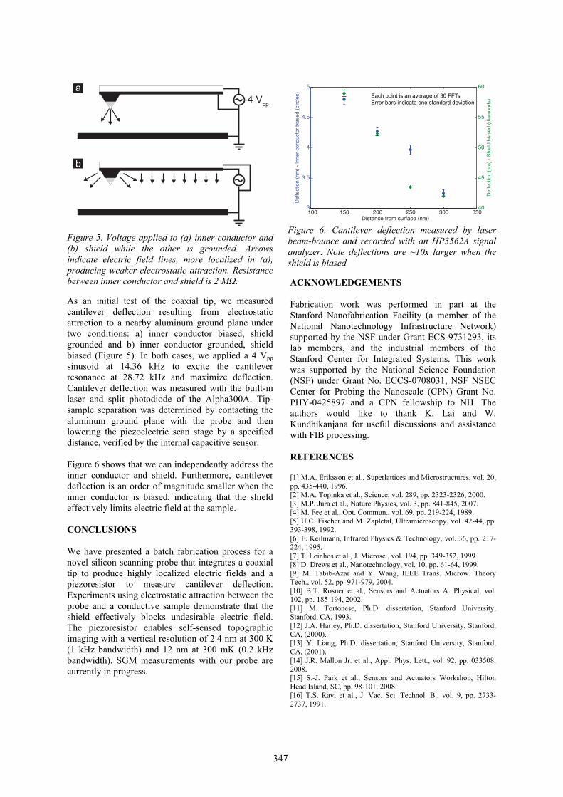
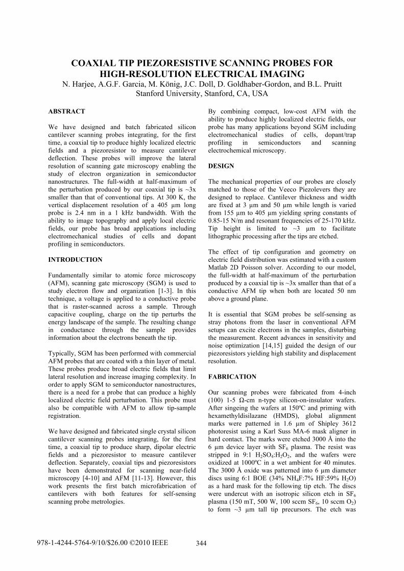
As an initial test of the coaxial tip, we measured cantilever deflection resulting from electrostatic attraction to a nearby aluminum ground plane under two conditions: a) inner conductor biased, shield grounded and b) inner conductor grounded, shield biased (Figure 5). In both cases, we applied a 4 Vpp sinusoid at 14.36 kHz to excite the cantilever resonance at 28.72 kHz and maximize deflection. Cantilever deflection was measured with the built-in laser and split photodiode of the Alpha300A. Tip-sample separation was determined by contacting the aluminum ground plane with the probe and then lowering the piezoelectric scan stage by a specified distance, verified by the internal capacitive sensor. Figure 6 shows that we can independently address the inner conductor and shield. Furthermore, cantilever deflection is an order of magnitude smaller when the inner conductor is biased, indicating that the shield effectively limits electric field at the sample. CONCLUSIONS We have presented a batch fabrication process for a novel silicon scanning probe that integrates a coaxial tip to produce highly localized electric fields and a piezoresistor to measure cantilever deflection. Experiments using electrostatic attraction between the probe and a conductive sample demonstrate that the shield effectively blocks undesirable electric field. The piezoresistor enables self-sensed topographic imaging with a vertical resolution of 2.4 nm at 300 K (1 kHz bandwidth) and 12 nm at 300 mK (0.2 kHz bandwidth). SGM measurements with our probe are currently in progress.
ACKNOWLEDGEMENTS Fabrication work was performed in part at the Stanford Nanofabrication Facility (a member of the National Nanotechnology Infrastructure Network) supported by the NSF under Grant ECS-9731293, its lab members, and the industrial members of the Stanford Center for Integrated Systems. This work was supported by the National Science Foundation (NSF) under Grant No. ECCS-0708031, NSF NSEC Center for Probing the Nanoscale (CPN) Grant No. PHY-0425897 and a CPN fellowship to NH. The authors would like to thank K. Lai and W. Kundhikanjana for useful discussions and assistance with FIB processing. REFERENCES [1] M.A. Eriksson et al., Superlattices and Microstructures, vol. 20, pp. 435-440, 1996. [2] M.A. Topinka et al., Science, vol. 289, pp. 2323-2326, 2000. [3] M.P. Jura et al., Nature Physics, vol. 3, pp. 841-845, 2007. [4] M. Fee et al., Opt. Commun., vol. 69, pp. 219-224, 1989. [5] U.C. Fischer and M. Zapletal, Ultramicroscopy, vol. 42-44, pp. 393-398, 1992. [6] F. Keilmann, Infrared Physics & Technology, vol. 36, pp. 217-224, 1995. [7] T. Leinhos et al., J. Microsc., vol. 194, pp. 349-352, 1999. [8] D. Drews et al., Nanotechnology, vol. 10, pp. 61-64, 1999. [9] M. Tabib-Azar and Y. Wang, IEEE Trans. Microw. Theory Tech., vol. 52, pp. 971-979, 2004. [10] B.T. Rosner et al., Sensors and Actuators A: Physical, vol. 102, pp. 185-194, 2002. [11] M. Tortonese, Ph.D. dissertation, Stanford University, Stanford, CA, 1993. [12] J.A. Harley, Ph.D. dissertation, Stanford University, Stanford, CA, (2000). [13] Y. Liang, Ph.D. dissertation, Stanford University, Stanford, CA, (2001). [14] J.R. Mallon Jr. et al., Appl. Phys. Lett., vol. 92, pp. 033508, 2008. [15] S.-J. Park et al., Sensors and Actuators Workshop, Hilton Head Island, SC, pp. 98-101, 2008. [16] T.S. Ravi et al., J. Vac. Sci. Technol. B., vol. 9, pp. 2733-2737, 1991.
Figure 6. Cantilever deflection measured by laser beam-bounce and recorded with an HP3562A signal analyzer. Note deflections are ~10x larger when the shield is biased.
Figure 5. Voltage applied to (a) inner conductor and (b) shield while the other is grounded. Arrows indicate electric field lines, more localized in (a), producing weaker electrostatic attraction. Resistance between inner conductor and shield is 2 MΩ.
100 150 200 250 300 3503
3.5
4
4.5
5
Def
lect
ion
(nm
) - In
ner c
ondu
ctor
bia
sed
(circ
les)
Distance from surface (nm)
40
45
50
55
60
Def
lect
ion
(nm
) - S
hiel
d bi
ased
(dia
mon
ds)Each point is an average of 30 FFTs
Error bars indicate one standard deviation
a
b
4 Vpp
347