co2 module - frank's hospital...
TRANSCRIPT

CO2 MODULE
INTRODUCTIONThis area contains component information about theModel 7345 CO2 Module. The CO2 Module monitorsthe partial pressure of respiratory carbon dioxide. Itmeasures the absorption of infrared light byrespiratory gases and calculates endtidal carbondioxide (ETCO2) and inspired CO2. A samplingpump allows monitoring of a mainstream orsidestream sample of airway gases. Respirationrate is calculated by measuring the time intervalsbetween peaks of the CO2 waveform. The displayedrate is the result of averaging the inverse of the 8most recently detected time intervals.
The CO2 Module provides automatic compensationfor the effect of barometric pressure on the CO2reading, user-selectable compensation for thepresence of more than 60% oxygen and thepresence of more than 50% nitrous oxide, and theability to modify the detection algorithm tocompensate for artifact-induced waveforms.

PHYSICALDESCRIPTION
The CO2 Module is shown in FO-7B. The Modulecontains a front panel with one patient connector andsampling pump inlet and outlet, a flex PWA, an OEMPWA, and a digital/power supply PWA. The flex PWAprovides power and signal connections from theOEM PWA to the front panel sensor connector.

FUNCTIONALPRINCIPLES OFOPERATION
A functional block diagram of the CO2 Module isshown in FO-7A. The diagram is divided intoisolated circuitry and non-isolated circuitry. Theisolated circuitry includes the CO2 sensor, the flexPWA, and the OEM PWA. The isolated (ISO)interface and push-pull transformer isolate thiscircuitry from the non-isolated core logic. The corelogic provides communication between the systemhost and CO2 Module through the PNet synchronousserial interface. It also controls data acquisition anddata processing functions for the CO2 monitoringchannel.
Isolated CircuitsIsolated circuits are shown in the top half of FO-7A.The sampling pump receives power from the OEMPWA through the front panel connector. Power fromthe Module is applied to an infrared (IR) light emitterin the CO2 sensor. The signal from an IR receptor inthe CO2 sensor is received through the front panelconnector and is connected to the OEM PWA via theflex PWA.
The isolated interface provides an isolatedasynchronous serial communication channelbetween the core logic and the OEM PWA. Theisolated power block consisting of isolated +12V,+5V, and two -12V power supplies provides isolatedpower to the OEM PWA and the sensor connectedcircuitry.
Non-Isolated CircuitsNon-isolated circuits are shown in the bottom half ofFO-7A. Functional blocks include the PNet interface,pulse width modulator (PWM) and power switcher,isolated power control, reset/failsafe, 68302 CPU,128Kx8 data memory, 128Kx8 program memory, themodel and serial number EEPROM, and logicanalyzer/test interface.
Power (+12V and +5V), is received through J1. The+12V is applied to the PWM and power switcher thatpowers the isolated circuitry. ISO power control

limits the PWM power-on until after the CPU is resetand shuts down the PWM if a failsafe conditionoccurs.
The Module will not be damaged when plugged intoa live slot. Core logic power inputs to a Module arelimited to a peak inrush current during hot-plugging.Within 2 seconds the Module responds toidentification and wakes up in a minimized powerstate until registered with the system.
The PNet interface allows asynchronous andsynchronous data transfer between the core logicand the external devices. Synchronous operation isalways used in MPS systems. Asynchronousoperation is for test and development only. Thereset/failsafe logic provides power-on reset,processor reset and halt, and failsafe if a problemoccurs with the microprocessor. Themicroprocessor controls and transfers data withinthe core logic. The program memory is a FLASHdevice that can be loaded with program informationfrom the PNET interface or the logic analyzerinterface. Data memory temporarily stores statusand monitoring data for processing.
COMPONENTPRINCIPLES OFOPERATION
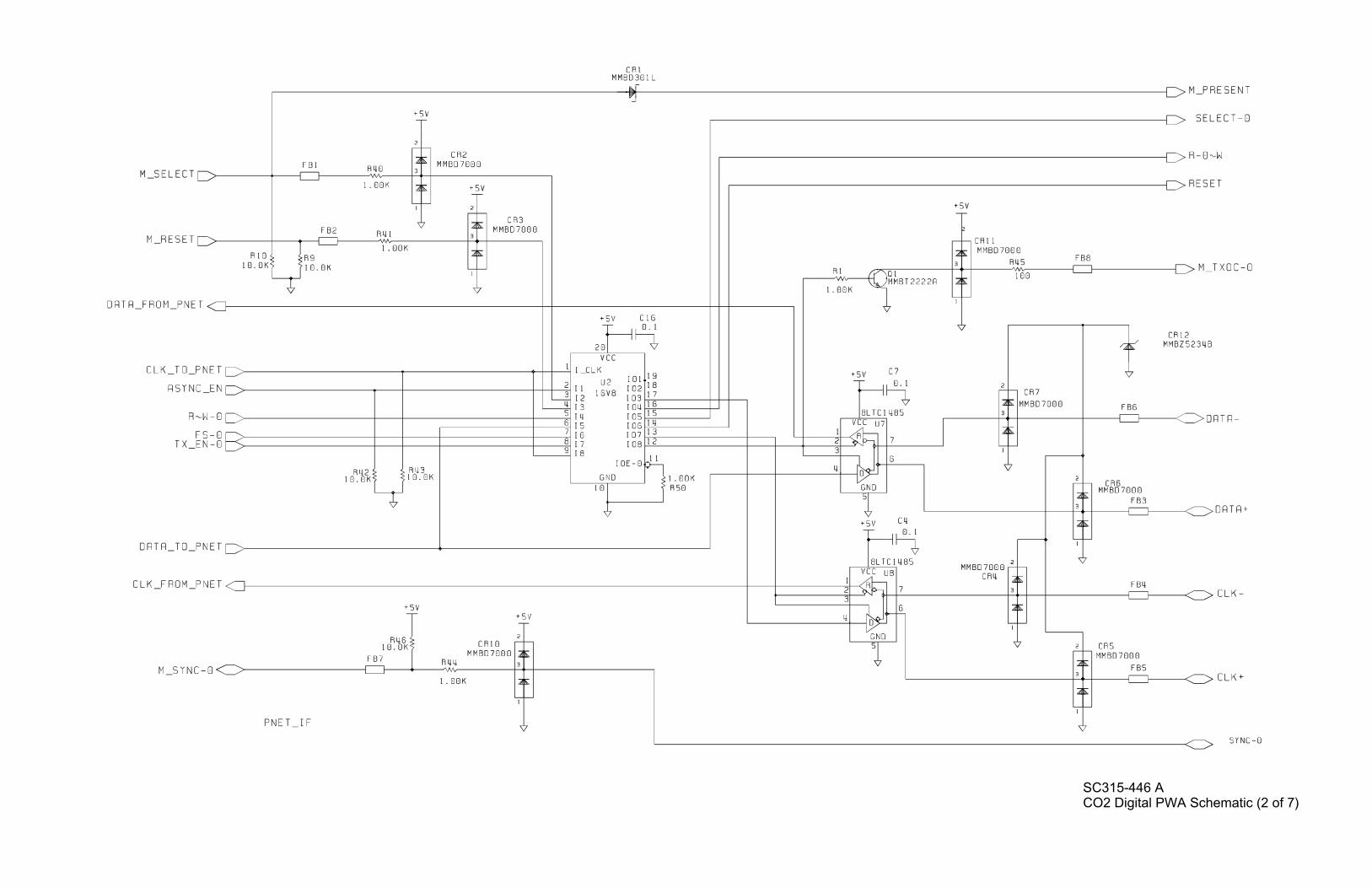
Schematic diagram SC315-446 is provided. Thefirst sheet of the schematic shows an overall blockdiagram of the CO2 digital PWA.
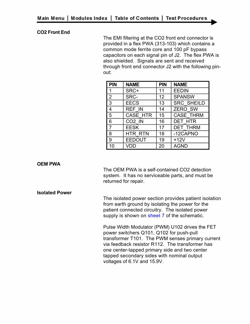
CO2 Front EndThe EMI filtering at the CO2 front end connector isprovided in a flex PWA (313-103) which contains acommon mode ferrite core and 100 pF bypasscapacitors on each signal pin of J2. The flex PWA isalso shielded. Signals are sent and receivedthrough front end connector J2 with the following pin-out:
PIN NAME PIN NAME1 SRC+ 11 EEDIN2 SRC- 12 SPANSW3 EECS 13 SRC_SHEILD4 REF_IN 14 ZERO_SW5 CASE_HTR 15 CASE_THRM6 CO2_IN 16 DET_HTR7 EESK 17 DET_THRM8 HTR_RTN 18 -12CAPNO9 EEDOUT 19 +12V10 VDD 20 AGND
OEM PWAThe OEM PWA is a self-contained CO2 detectionsystem. It has no serviceable parts, and must bereturned for repair.
Isolated PowerThe isolated power section provides patient isolationfrom earth ground by isolating the power for thepatient connected circuitry. The isolated powersupply is shown on sheet 7 of the schematic.
Pulse Width Modulator (PWM) U102 drives the FETpower switchers Q101, Q102 for push-pulltransformer T101. The PWM senses primary currentvia feedback resistor R112. The transformer hasone center-tapped primary side and two centertapped secondary sides with nominal outputvoltages of 6.1V and 15.9V.

Short-circuit protection for the isolated powersupplies is provided by the pulse-to-pulse currentlimit feature of the PWM. Resistor R112 senses thecurrent through power switchers Q101 and Q102,R116 and C122 filter out the switching spikes in thevoltage across R112, and resistors R114 and R115set the current limit value of the PWM. The PWM willfunction normally once the short is removed.
The PWM is synchronized to the Core Logic clock(200 KHz) by TIMER2 output from the CPU.Removing R143 allows the PWM to free runasynchronously at approximately 100KHz.
The output of the PWM is the logical OR of FS-1 andISO_PS_ON-0. During power-on, ISO_PS_ON-0remains pulled up until the CPU comes out of thereset state. During failsafe conditions, FS-1 isasserted, and the ISO_PS is shut down.
The 6.1V from the secondary of push-pulltransformer T101 is bridge rectified by CR101 andCR102 to give approximately +5.3Vdc. This voltageis then regulated using U101a and controlled powerFET Q109 to give +5Vdc (ISO_+5V). Op-amp U101gets a precision reference of +5V from REF02 U105.
The 15.9V from the secondary of isolationtransformer T101 is bridge rectified by CR103 andCR104 to give approximately+15Vdc, and CR105and CR106 to give approximately -15 Vdc. The+15Vdc is regulated by op-amp U104a andcontrolled power FET Q105 to give regulated +12Vdc(ISO_+12V). The +12V regulator gets a precisionreference of +5V from REF02 U105. The -15Vdc isregulated by op-amp U104b and controlled powerFET Q104 to give regulated -12Vdc (ISO_-12V1). Asecond, independent, low power -12V output (ISO_-12V2) is implemented with regulator U106.

Op-amp U104b used in the -12Vdc regulator gets anon-inverting input from instrumentation amplifierU103, which scales the difference in voltagebetween the +12V and -12V outputs to a 4.9Vnominal output. Window comparators U112a andU112b generate POWER_GOOD when the output ofU103 is 4.9V ±2%. POWER_GOOD from U112 issent back to the Core Logic CPU via optocouplerU110. If the output from U103 falls out of the 4.9V±2% range, POWER_GOOD goes false and signalsthe Core logic CPU to shut down the power supply.
Isolated InterfaceAs shown on sheet 7 of the schematic, opto-couplers U107 and U108 provide a full duplex,isolated serial channel between the non-isolatedcore logic and the isolated circuitry as ISO_DATA_INand ISO_DATA_OUT. Q107 and Q108 buffer thesignal to the opto-couplers. U110 couples thePOWER_GOOD signal across the isolated interface.
Core LogicThe core logic is shown on sheets 2 through 6 of theschematic. The core logic provides communicationbetween the system host and Module through thePNet synchronous serial interface. It also controlsdata acquisition and data processing functions forthe CO2 sensor. The Module is an 8-bit version ofthe core logic with one 128Kx8 RAM and 128Kx8ROM device. The microprocessor runs at 9.869MHz.
PNet Interface
The PNet interface, shown on sheet 2 of theschematic, provides the following functions:
• RS485 drivers (U7 and U8) for serial data andclock,
• Module select and presence detection (U2),• Module synchronization.
Core signals are received on PNet connector J1(sheet 1) with the following pin-out:

PIN NAME PIN NAME1A,1B +5V 6B M_SELECT2A DATA+ 7A M_PRESENT2B DATA- 7B TXOC-03A,3B +3.3V 8A M_SYNC-04A CLK+ 8B -12V4B CLK- 10A,10B +12V5A,5B GROUND 1,2 GROUND6A M_RESET
The CO2 Module is designed to be inserted andremoved (‘hot-plugged’) from powered systems.Ground pins 1 and 2 are longer than the otherconnector pins, thus they make first and break last toprotect the circuitry. This is partially because ofprotective impedance located on the systembackplane, in series with the modules +5V and +12Vpower. Also series impedance on PNet control lineslimits inrush and protects logic devices fromexcessive currents during a hot-plug power up.
The PNet protocol defines two modes of operation:synchronous and asynchronous. The normal modeof operation is synchronous, with half duplextransmitted and received data on differential signalsDATA+ and DATA-. As shown on sheet 2 of theschematic, the device transmitting the serial dataalso generates differential clock signals CLK+ andCLK-. Transceiver direction for data and clock arecontrolled by the 68302 processor-generatedTX_EN-0 (low true transmit enable) signal throughU2. In the synchronous mode, both data and clocktransceivers U7 and U8 are set to receive (i.e.,transmit disabled) when fail-safe signal FS-0 isasserted.

The alternate serial mode, full duplex asynchronous,is entered by asserting processor generated controlbit ASYCH_EN. This mode transmits data onto thedifferential signals CLK+ and CLK-, and receivesdata from the differential signals DATA+ and DATA-.The transmitter in the Module is disabled unless theModule has been commanded to transmit per thePNet protocol. The Module transmitter isimmediately disabled after the last character of atransmission has been sent.
The Module select input (M_SELECT, hi true)instructs the Module to respond to identificationrequests. When both M_SELECT input andM_RESET input (hi true) are asserted, the Moduleperforms a hardware reset.
The Module present output, M_PRESENT isconnected to M_SELECT through diode CR1 to allowa means of determining if the Module is plugged intoan instrument. When M_SELECT is asserted(pulled hi) M_PRESENT is hi true.
Module transmitter open collector signal TXOC-0from Q1 signifies the Module transmitter is enabled.Serial data is then transmitted in the synchronousmode.
M_SYNC is used for timing of shorter latency periodsthan supported by the serial data protocols. AModule only asserts M_SYNC when enabled by thehost.
Reset Logic
The reset logic is shown on sheet 3 of theschematic. Reset logic U9 generates a power-on-reset when power is applied. RESET-0 AND HALT-0signals remain low for minimum of 130 msec afterall logic voltages are in specification.

External reset, processor reset, and halt signals arelow for minimum of 24 clocks when external resetasserted. Power monitoring, processor reset, andhalt signals are low if logic voltages drop belowspecification. They remain low for minimum of 130msec after logic voltages return to the specifiedrange.
The reset circuit consisting of U6b and U6d providesopen drain outputs to the processor bi-directionalreset and halt signals.
Fail-Safe Logic
Fail-safe latch (U6a and U6c) ensures that theModule enters a safe state if the processor fails tooperate correctly. The latch is set by a low true outputfrom the processor watchdog timer (WDOG-0). Thedata transmitter is disabled, isolated power is shutdown, and the Module remains in a safe state untilthe latch is cleared by a power on or external reset.
Microprocessor
The core logic design is based around the 68302microprocessor (U10) shown on sheet 4 of theschematic. The 68302 combines a 68000 core witha three channel communication processor, andsystem integration circuits.

The left side of the CPU contains clock interfacesto/from the PNet, port A, and port B to various circuitsin the core logic, reset, and halt interface. The IRQports are not used. The right side of the CPUcontains address and data lines and chip selectoutputs. The 68302 operates with a staticallydefined 8-bit wide bus. The following resources areused for specific Module functions:
CHIP SELECTS LOGICCS0-0 FLASH ROMCS1-0 STATIC RAM
SERIAL COMM CHANNELSSCC1 PNET
[RXD1, TXD1, RCLK1, TCLK1,CTS1-0, RTS1-0]
SCC2 ASYNC DEBUG [RXD2,TXD2]SCP SERIAL EEPROM
[SPRXD,SPTXD,SPCLK]TIMER1 SYSTEM TIMEBASE
PARALLEL IO / SPECIAL PURPOSE IO BITSPA2 CHIP SELECT TO SERIAL EEPROMPA5 ASYCN_EN (PNET MODE SELECT)PA6 POWER MANAGEMENT CONTROLPB5 /TIN2 TIMEBASE INPUT FOR EXTERNAL
MEMORY / SYSTEM CONFIGPB7 WATCHDOG TIMER OUTPUT
Program Memory
Program memory consists of 8-bit flash ROM U11shown on sheet 5 of the schematic. The ROM isconfigured for 128Kx8 (1024k bit). The ROM is notsocketed and can not be removed for programming.The ROM can be flash-programmed via the logicanalyzer interface or the PNET connector.

Data Memory
Data is stored in 128Kx8 static RAM U3 shown onsheet 5 of the schematic. This RAM is cleared whenpower is removed.
Non-Volatile Memory
Serial EEPROM U1 shown on sheet 5 of theschematic is a 128-byte PROM that provides non-volatile storage for model and serial numberinformation and parameter user interface data whichmust travel with the Module. The 68302 synchronouscommunication port (SCP) is used to access theEEPROM.
Logic Analyzer/Test Interface
The logic analyzer/test interface is shown on sheet 6of the schematic. The core logic includes aninterface to bring signals required for external ROMaccess, logic analyzer interface, and a debug serialchannel to a single connector.
The external ROM access allows an off board ROM(8 bit) or ROMs (16 bit) to replace the FLASH devicesat address 0. Address, data, and control signalsrequired for this function are included on the LA/Tconnector.
All signals needed for a Hewlett Packard model16500 logic analyzer or equivalent to perform busstate analysis and disassembly are included on theLA/T connector.
The 68302 SCC2 serial transmit and receive datasignals are included on the LA/T connector.

The LA/T connector pinouts are as follows:
PIN NAME PIN NAME1,69 +5V 2,28,45,46,7
0GND
3 A0 4 A15 A2 6 A37 A4 8 A59 A6 10 A711 A8 12 A913 A10 14 A1115 A12 16 A1317 A14 18 A1519 A16 20 A1721 A18 22 A1923 A20 24 A2125 A22 26 A2329 D0 30 D131 D2 32 D333 D4 34 D535 D6 36 D737 D8 38 D939 D10 40 D1141 D12 42 D1343 D14 44 D1547 DTACK-0 48 AS-049 RW 50 UDS-051 DS-0 52 BGACK-053 FC0 54 FC155 FC2 56 DEBUG TXD57 DEBUGRXD 58 EXROMCS-063 PRGM_EN 64 DISCPU65 T1_IN

DISASSEMBLYPROCEDURE
STATIC DISCHARGE CAUTION
Do not attempt to serviceunit without staticdischarge protection.Workstations andpersonnel must be properlygrounded, or damage toequipment will result.
1. Remove two 4-40 x 5-1/4" screws from the rearof the Module. Remove rear cover.
2. Slide enclosure toward rear of Module, andremove enclosure.
3. Remove insulators.
4. Pull two card guides away from PWA and shieldassembly, and remove guides.
5. Carefully separate digital PWA connector andshield assembly at top of Module.
6. Remove tubing from inlet of pump.
7. Remove tubing and wire wraps from outlet ofpump.
8. Remove pump connector from OEM PWA.
9. Remove 4-40 screw that secures flex assemblyto OEM PWA. Remove flex assembly by pulling itupward.

10. Disassemble OEM shield assembly bydisengaging each of the corner locking tabs(accessible through plastic shield ventopenings)
11. Using FO-7B as a guide, perform any additionaldisassembly that may be required formaintenance procedures.

REASSEMBLYPROCEDURE
1. Make sure that fastening tabs on emi shieldcover (44, FO-7B) for OEM PWA have not beendeformed. Reassemble OEM PWA and shieldassembly.
2. Secure pump. Push upper hose with filter ontopump inlet. If outlet tube was removed frombarbs, push lower hose onto pump and replacewire ties.
3. Install front panel flex PWA connector and securewith 4-40 screw (43) and lock washer (50).Route pump wires under flex stiffener as shownin View A of FO-7B, to ensure integrity of patientsafety isolation.
4. Install digital PWA in front panel slot, andconnect 10-conductor interface connector.
5. Carefully hold PWA and shield assemblytogether, and push upper and lower card guidesonto slots. Install insulators.
6. With enclosure oriented so large groove is atbottom and label is at right (viewed from front ofModule), slide enclosure over PWAs and shieldassembly.
7. Install back cover on the Module enclosure.
8. Fasten the front and rear covers to the enclosureby inserting two 4-40 x 5-1/4" screws from therear through the enclosure to the front cover asshown in FO-7B. Tighten the two screws to 4-in/lb.
SAMPLING SYSTEMCLEANINGPROCEDURE
Whenever required, perform the steps listed belowto clean and sterilize internal sampling systemcomponents. Compatible cleaning and disinfectingsolutions are:
• Chlorine bleach disinfectant, 5.25%, variousbrands, 0.75 cup per gallon of water
• Isopropyl alcohol
• Cidex Formula 7® or pHisoHex®
• Quatenary-based germicidal detergents likeVESTAL INSURANCE®, HI-TOR PLUS®, orVIREX®
For the above, follow manufacturers'recommendations for dilution rate and use. Theserecommendations are not an endorsement of themanufacturers or of the effectiveness of thesematerials for cleaning or disinfecting.
CAUTION
Do not attempt to pump cleaning andsterilizing liquids using the sampling pump.This may cause accelerated wear on thepump bearings. Always flush liquids with asyringe, as described below.
1. Turn off the Monitor and disconnect the powercord.
® Cidex Formula 7 is a registered trademark of Johnson & Johnson MedicalProducts, Inc. pHisoHex is a registered trademark of Winthrop-BreonLaboratories. VESTAL INSURANCE is a registered trademark of the Vestal Corp.HI-TOR PLUS is a registered trademark of the Huntington Corp. VIREX is aregistered trademark of S.C. Johnson & Son Corp.
2. Remove both the sampling inlet tubing set andthe sampling exhaust tubing, if any.
3. Attach an exhaust port line (1/8 inch ID tubing or3/16 inch ID tubing) from the sampling exhaustport to a suitable container located below thebottom level of the Monitor.
4. Fit a 60 cc catheter tip syringe to the samplinginlet connector. Flush the sterilizing solutionslowly through the pumping system. Push theentire 60 cc of solution through the inlet. Repeatthis process twice, until about 180 cc of solutionis used.
5. Remove the syringe, and leave the cleaning orsterilizing fluid within the sampling pump systemfor 30 minutes (for a disinfectant), or for as longas recommended by the manufacturer if asterilizer is used.
6. After 30 minutes, fill the syringe with distilledwater and flush the system three times. Allowthe cleaning or sterilization solution and distilledwater to drain through the sampling exhaustoutlet.
7. Push several syringes of air slowly through thesystem to ensure that most of the liquid hasbeen drained.
8. Follow this with at least three more flushes ofdistilled water, then push through at least twosyringes of air to ensure most of the distilledwater has been drained.
9. Remove the syringe from the unit. While thesampling inlet tubing is still disconnected,connect the Monitor power cord and power it on.Allow the sampling pump to operate for severalminutes. This will help to remove any trappedwater.

10. Connect a sampling tube set to the samplinginlet.
11. Block the open end of the tubing with your finger.Alternately block and clear the tubing at least tentimes, each time for several seconds, using aquick, brisk motion.
12. Block the open end of the sampling exhaust port,and block and clear this port in the same waydescribed above.
13. To speed up drying the system pneumatics,allow the sampling system to run without anysampling inlet or exhaust tubing for at least 30minutes.

PARTS LISTSTop Assembly 7345 parts are listed in Table 7-1 andshown in FO-7B. CO2 Digital PWA 315-446 partsare listed in Table 7-2 and shown in FO-7C.
Table 7-1. Top Assembly 7345 Parts List
Item Description Part No.1 COVER, PARAMETER REAR 703-1882 SUB-ASSY, ENCLOSURE, EXTRUDED SW 320-6763 PANEL, FRONT, C02 701-4164 PWA, FLEX, FRONT PANEL, C02 313-1035 TUBING PHARMED 740-1856 FILTER, AIR,43 MICRON STAINLESS FILTER 754-1367 HOSE BARB FITTING 754-1208 LUER, FEMALE 712-2569 HOSE BARB, ADJUSTABLE 754-14515 PWA, C02 DIGITAL 315-44619 SCREW, RDH PHH, 4-40X51/8, CUSTOM 722-20120 INSULATION, GUIDE, MODULE 750-18222 SCREW, 2-56X3/16 PNH PHH SST 719-23724 SCREW, 4-40X1/4 PNH PHH SST 719-10226 BUTTON, LATCH, SW 73216627 SPRING, CONTACT, GROUND 736-20430 GASKET, CONNECTOR, C02 703-19333 NOVA/SHIELD ASSY 320-66934 INSULATOR, DIGITAL 750-18936 FITTING,TUBE,NYLON 712-26837 TUBING POLYURETHANE 5/32 0D X 5/64 ID 740-19738 INSULATOR, NOVA, CAN 750-19139 PUMP,AIR,12V DC MOTOR 712-26540 SCREW,2-56X3/16 100DEG FH 719-23941 PAD, MOTOR MOUNT 752-26643 SCREW, 4-40X3/8 PNH, PHH,SST 722-22944 SHIELD, EMI, METAL C02 737-18345 PWA, CO2 OEM, NOVAMETRIX 645-17146 TYWRAP NYLON .75 BDL DIA.MAX. 756-10147 TUBING,TYGON 3/32 ID X 5/32 OD 740-19948 TUBING,TYGON 3/16 ID X 1/4 OD 740-20049 INSULATOR, NOVA PWB 750-19250 WASHER, LOCK, FL-INT TOOTH SST # 4 724-10651 WASHER, LOCK, FL-INT TOOTH # 2 724-115

Table 7-2. CO2 Digital PWA 315-446 Parts List
Item Description Part No.C1 CAP,2917/D,TANT,35V,20%,10 UF 606-188C2,C3 CAP,CER,SMD,0603,NPO,10%,50V,27 PF 605-718C4-16,101-107,109,110,112,121,125-128,134,135
CAP,CER,SMD,0805,X7R,10%,50V,0.10 UF 605-533
C111,113-115 CAP, ELCTLT, 100 UF, 16V, SMD 604-191C117-119,129 CAP, ELCTLT, 68 UF, 35V, SMD 604-190C120 CAP,CER,SMD,0603,NPO,10%,50V,220 PF 605-729C122,124 CAP,CER,SMD,0603,X7R,10%,50V,1000 PF 605-809C130,131,133 CAP,CER,SMD,0603,Z5U,20%,50V,0.033 UF 605-919CR1,13 DIODE, SCHOTTKY, 30V, 200MW, SOT-23 611-137CR2-7,10,11 DIODE, DUAL SERIES SMT SOT-23 611-140CR12 DIO ZENER 6.2V, 5% SMT, 225MW 612-147CR101-106 DIODE, RECT-SCHOTTKY, 3A, 40V, SMT 611-145FB1-9,100 FERRITE CHIP, EMI SUPPRESSION, SMT 669-170J1 CONN, 20 PIN PLUG RT ANGLE PC MOUNT 607-795J2 CONNECTOR, 10 CONDUCTOR 608-344J4 SOCKET, MICRO STRIP 35X2, SMD 607-816L101 INDUCTOR, 10UH 20% 2.6A 0.06 DCR SMD 669-205Q1 XST NPN 2222A SMT 674-127Q101,102,104,109
XSTR, POWER FET, TMOS, N-CHANNEL DPAK 676-157
Q105 XSTR, PWR, NPN, DARLINGTON SMD 673-116Q107,108 XST PNP SMT 674-126R1,40,41,44,50,128,130
RES,0603,1/16W,1%,1.00K OHM 686-293
R2 RES,0603,1/16W,1%,4.99K OHM 686-360R3,4,7-33,35,42,43,46,47,48,102,111,117
RES,0603,1/16W,1%,10.0K OHM 686-389
R5,6,126,129,144
RES,0603,1/16W,1%,2.21K OHM 686-326
R34 RES,0603,1/16W,1%,698K OHM 686-566R45 RES,0603,1/16W,1%,100 OHM 686-197R105,106,110,121,122
RES,0603,1/16W,1%,10.0 OHM 686-101
R107,108 RES,0603,1/16W,1%,100K OHM 686-485R112 RES,2512,1W,1%,0.1 OHM 686-607R113 RES,0603,1/16W,1%,12.7K OHM 686-399

Table 7-2. CO2 Digital PWA 315-446 Parts List (Continued)
Item Description Part No.R114 RES,0603,1/16W,1%,49.9K OHM 686-456R115 RES,0603,1/16W,1%,20.0K OHM 686-418R116 RES,0603,1/16W,1%,1.40K OHM 686-307R118,120,135 RES,0805,1/10W,0.1%,21.5K 685-629R119 RES,0805,1/10W,0.1%,11.0K 685-630R123 RES,0805,1/10W,0.1%,3.57K 685-628R124 RES,0805,1/10W,0.1%,4.99K 685-623R127,131,141 RES,0603,1/16W,1%,750 OHM 686-281R132 RES,SMD,1/10W,JUMPER 0.0 OHM 685-606R133,134 RES,0603,1/16W,1%,442 OHM 686-259R136,137 RES,0603,1/16W,1%,6.04K OHM 686-368R138,140 RES,0603,1/16W,1%,1.0M OHM 686-581R142,143 RES,0603,1/16W,JUMPER 0.0 OHM 686-606T101 XFORMER, POWER HI-FREQUENCY, TOROID 668-164U1 IC,93C56 2KBIT SERIAL EEPROM,CMOS SM 692-183U2 IC, EECMOS PLD 16V8B, ARRAY LOGIC 692-226U3 IC, 128X8 70NS CMOS SRAM TSOP 694-133U4 IC,74AC32 QUAD 2 IN OR GATE,ADV CMOS SM 692-141U6 IC,74HC03 QUAD 2 IN.NAND,CMOS SUF MT 692-139U7,8 IC, CMOS LTC1485, DIFF BUS XCEIVER SO8 692-225U9 IC, POWER SUPPLY MONT WITH RESET SMT 694-118U10 IC, 68302 INTEGRATED PROCESSOR 144 SMT 694-130U101,104 IC, OP-AMP, DUAL/QUAD, PRECISION SMD 691-141U102 IC, LO-POWER, PWM, CURRENT MODE SMD 693-166U103 IC, AD620BR, INSTRUMENTATION AMP, SMT 692-187U105 IC, 5V REG/TEMP XDCR, SMD 693-121U106 IC, -12V VOLTAGE REG SOIC 693-167U107,108,110 IC, HCPL-2611, OPTOCOUPLERS, SMT 695-101U109 IC, 128K X 8-BIT 5V FLASH ROM CMOS SMT 692-195U111 IC, SMT, DUAL D FLIP FLOP 692-117U112 IC, DUAL COMPARATOR SMD 693-158Y100 CRYSTAL, 9.869MHZ, 0.005% HC-49UP 609-129#16 PAL_U2A, CORE LOGIC 637-101

ISOLATED INTERFACE
RESET/FAILSAFE
U6, U9
ADDRESS 0-23
DATA 0-7
J4-29J4-36
J4-3J4-26
PROGRAM ENABLE
DEBUGDATA
LOGIC ANALYZER
TESTINTERFACE
7A
6B
6A
7B
8A
4A
4B
2A
2B
M_PRESENT
M_SELECT
M_RESET
TXOC-0
M_SYNC-0
CLK+
CLK-
DATA+
DATA-
PNETINTERFACE
Q1, U2,U7, U8
CO2 FLEXCONNECTOR
TRANSFORMERT101
ISOPOWER CONTROL
ISOLATED CIRCUITRY
NON-ISOLATED CIRCUITRY
J1
10A
10B
1A1B
+12V
+5V
5A5B
1,2
R/W
CLOCK & DATA TO/FROM PNET
SELECT
RESET
HALT
RESET
FAILSAFE-0
MODEL &SERIAL NUMBER
EEPROMU1
CO2 HOSTMODULE
10
9
P/OJ2
P/O J2
SAMPLINGPUMP
IREMITTER
RECEPTOR
TRANSMIT ENABLE
PORT B (0-15)
SP DATA
SP CLOCKFAILSAFE-1
PULSE MODULATOR, ANDPOWER SWITCHERU102, Q101, Q102
+VIN
+5VREGULATORP/O U101,
Q109
J1
POWERGOOD
U112
POWER_GOOD
EMI SHIELD
POWERSUPPLYSYNCU111
J2
CO2 SENSOR
INLET
EXHAUST
U10
FO-7A. CO2 Module Block Diagram
FLASHROMU109RAM
U3
U4
200 KHZ
200 KHZ
9.869 MHZ
1 MHZ
-12V2 REGULATORU106 +12V REGULATOR
-12V1 REGULATOR
Q107, Q108, U107,U108, U110
U103,
Q104, U104
U105, U104, Q105

FO-7B. Top Assembly 7345

FO-7C. CO2 Digital PWA 315-446

SC315-446 ACO2 Digital PWA Schematic (1 of 7)
SC315-446 ACO2 Digital PWA Schematic (2 of 7)

SC315-446 ACO2 Digital PWA Schematic (3 of 7)

SC315-446 ACO2 Digital PWA Schematic (4 of 7)

SC315-446 ACO2 Digital PWA Schematic (5 of 7)

SC315-446 ACO2 Digital PWA Schematic (6 of 7)

SC315-446 ACO2 Digital PWA Schematic (7 of 7)