cmp challenges in sub-14nm finfet and rmg technologies€¦ · cmp challenges in sub-14nm finfet...
TRANSCRIPT

CMP challenges in sub-14nm FinFET and RMG technologies
NCCAVS CMPUG Spring Meeting 2016
Tae Hoon Lee*, Hong Jin Kim, Venugopal Govindarajulu, Gerett Yocum
& Jason Mazzotti
Advanced Module Engineering

Contents
• Sub 14nm Logic Device Roadmap
• FEOL CMP Process Flow and CMP Challenges
• RMG (Replacement Metal Gate) Process Flow and CMP Challenges
• Challenges on Post CMP Cleaning Optimization
• CMP Challenges for Cost Reduction
• Functional Advanced CMP Equipment
• Summary

CMOS Transistor Scaling

New Device Platform
Materials Innovation of Technology Node. Source: Bartlett, GLOBALFOUNDRIES, SEMI Strategic Materials Conference 2013

FinFET (Fin Field Effect Transistor) Introduction
FinFET:
- Foot-print: Smaller.
- Better gate control (less SC-effect)
- Higher Ion and Lower Ioff.
- Easier device tuning.
Planar CMOS:
- Poor gate control (SC-effect).
- Higher Ioff.
- Difficult in device tuning.
- Last generation on planar CMOS.
K. Ahmed & K. Schuegraf, “Transistor wars: Rival architectures face off in a bid to keep Moore’s Law al ive”, IEEE Spectrum, Nov. p.50, 2011.

6
FinFET transistors:
- Channel:
Fully depleted with both the
surface and volume inversion.
-Mobility:
good for high performance.
- Vt: determined by gate work-
function; less mismatch;
- Short-channel effect:
significantly reduced (low Ioff,
good DIBL, SS).
- Next generation:
Device of choice at 14nm (and
beyond) for high performance and
low power applications.
K. Ahmed & K. Schuegraf, “Transistor wars: Rival architectures face off in a bid to keep Moore’s Law al ive”, IEEE Spectrum, Nov. p.50, 2011.
FinFET has strong gate control on channel

7
Low power consumption
More current due to increase in conductive region between source
and drain which implies charge current during ON state and high
speed
More Gate control which implies less OFF state leakage current
FinFET Device Manufacturing

FinFET Scheme and FEOL Process Flow
Poly deposition
Poly mandrel formation
STI spacer and FIN patterning
FIN STI CMP and FIN reveal
Poly deposition
Poly CMP

Challenges of Poly CMP
WIW uniformity control
- Tight control poly height at post CMP
- High selective slurry required (poly stop slurry)
- New process scheme for minimum amount of poly loss
High Planarity
- Post poly CMP dishing/erosion getting worse until RMG formation
- Self-stop slurry for low topography variation
Surface roughness minimize
Poly CMP is the first step to determine gate height

RMG Process Flow
PC formation
Poly open CMP
Poly etch (removal)
Barrier and Metal (W) deposition
Metal (W) gate CMP
ILD deposition

Challenges in Poly Open CMP
Poly open CMP is the last step to determine gate height before WG CMP
Incoming height variation: variation in multiple upstream processes add up
- Gate poly thickness variation
- Poly etch variation
Complex process sequence
- ILD CMP Stop on Nitride ILD2 CMP Poly Open CMP (2 or 3 steps)
- Accurate endpoint
- High selectivity and high planarity
Post POC defect
- Residual oxide (or nitride) Blocking poly removal
- Microscratch PC (gate) to TS (contact) bridge
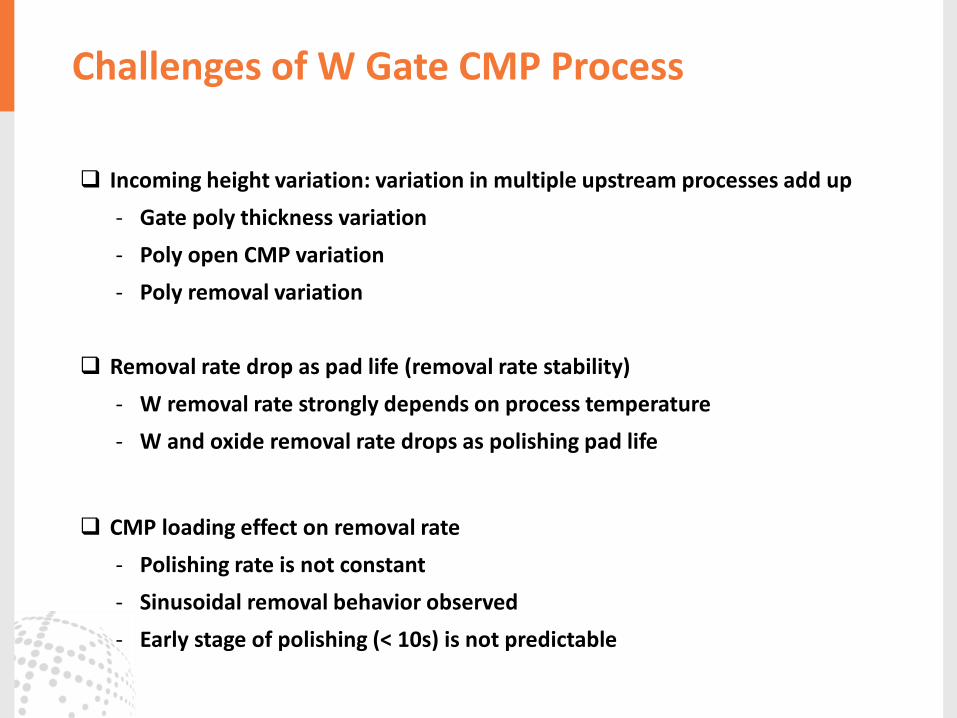
Challenges of W Gate CMP Process
Removal rate drop as pad life (removal rate stability)
- W removal rate strongly depends on process temperature
- W and oxide removal rate drops as polishing pad life
Incoming height variation: variation in multiple upstream processes add up
- Gate poly thickness variation
- Poly open CMP variation
- Poly removal variation
CMP loading effect on removal rate
- Polishing rate is not constant
- Sinusoidal removal behavior observed
- Early stage of polishing (< 10s) is not predictable

13
• Major defects induced by CMP are: 1)organic residue, 2)surface particle,
3)scratch, 4)surface flake, 5)grain roughness and 6)pattern damage
• Due to no redundancy, each defect directly has an impact on the device
performance or yield all kinds are potential killer defect
• Organic residue and surface particle are the most frequently observed
• Post W CMP defects are strongly dependent on post in-situ cleaning process
• Consumables for minimal defect are required: ultra-fine/colloidal abrasive or
abrasive-free slurry, soft pad without sacrificing planarity, mild conditioning with
proper pad surface roughness
• In-situ clean from CMP tool is the most effective for clean wafer since it cleans
wafer with wet state
Defect from CMP Process

Post in-situ Cleaning Optimization
• Brush: nodule hardness and porosity softer brush (material
property) with optimum porosity
• Nodule design, nodule height uniformity, nodule surface
treatment and optimum contact area minimize brush cross
contamination to wafer
• Brush gap, rotational speed, and chemical flow rate
• Friction between wafer and brush
• Brush loading brush breakin (pre-broken brush preferred)

Summary
• Sub-14nm device fabrication requires robust CMP process
• FinFET transistor formation is highly dependent on all front end of line CMPs and gate CMP (so-called replacement metal gate (RMG))
• Defect control is tremendous requirement for yield improvement
• Tight gate height control cannot be achieved by fixed time CMP due to multiple incoming and CMP process variability
• Advanced process control self-learning function enabled to get tight gate height control at post CMP by combining CMP tool with on-board metrology
• More advanced functional CMP technology is required for more robust process and for improved process window

Trademark Attribution
GLOBALFOUNDRIES®, the GLOBALFOUNDRIES logo and combinations thereof, and GLOBALFOUNDRIES’ other trademarks and service marks are owned by GLOBALFOUNDRIES Inc. in the United States and/or other jurisdictions. All other brand names, product names, or trademarks belong to their respective owners and are used herein solely to identify the products and/or services offered by those trademark owners.
© 2013 GLOBALFOUNDRIES Inc. All rights reserved.
Thank you [email protected]