cmos operational amplifier design - eecs at uc berkeley | · pdf filecmos operational...
TRANSCRIPT
CMOS Operational Amplifier Design
Navid Gougol
Electrical Engineering and Computer SciencesUniversity of California at Berkeley
Technical Report No. UCB/EECS-2016-223http://www2.eecs.berkeley.edu/Pubs/TechRpts/2016/EECS-2016-223.html
December 31, 2016
Copyright © 2016, by the author(s).All rights reserved.
Permission to make digital or hard copies of all or part of this work forpersonal or classroom use is granted without fee provided that copies arenot made or distributed for profit or commercial advantage and that copiesbear this notice and the full citation on the first page. To copy otherwise, torepublish, to post on servers or to redistribute to lists, requires priorspecific permission.
EE240A Design Project
Electrical Engineering and Computer Sciences Dept
UC Berkeley
CMOS Operational Ampli!er Design
Done by:
Navid Gougol
UID 1083826
Fall 2014
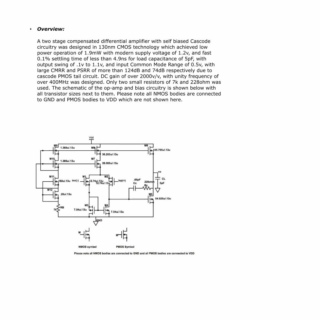
• Overview:
A two stage compensated differential amplifier with self biased Cascode
circuitry was designed in 130nm CMOS technology which achieved low
power operation of 1.9mW with modern supply voltage of 1.2v, and fast
0.1% settling time of less than 4.9ns for load capacitance of 5pF, with
output swing of .1v to 1.1v, and input Common Mode Range of 0.5v, with
large CMRR and PSRR of more than 124dB and 74dB respectively due to
cascode PMOS tail circuit. DC gain of over 2000v/v, with unity frequency of
over 400MHz was designed. Only two small resistors of 7k and 228ohm was
used. The schematic of the op-amp and bias circuitry is shown below with
all transistor sizes next to them. Please note all NMOS bodies are connected
to GND and PMOS bodies to VDD which are not shown here.

• Design:
As depicted in the circuit above, a two stage op-amp was designed with first
stage as a differential single ended op-amp with current mirror loading, and
second stage a common source stage. Tail of first stage was designed in
PMOS to achieve high PSRR [1]. Cascode tail was designed for differential
pair due CMRR requirements. As a result of tail cascode, Sooch current
mirror[2] was used to bias the cascode with low power consumption of only
11uW in bias circuit. To achieve fast slewing per 5ns settling time
requirement, second stage was biased in large bias current. Discussion of
the design will be provided in Discussion section of the report. To have fast
settling time and stability in unity feedback configuration, phase margin of
75 degrees[3] was designed, using miller capacitance with nulling resistor
technique[4]. Per compensation technique used, the zero generated was
used to cancel the second pole, leaving first dominant pole and 3rd pole the
only poles in the system. The details of design of each part will be given in
Discussion section of the report.
• Transistor and Bias Summary:
M1 M2 M3 M4 M5 M6 M7 M8 M9 M10 M11 M12
W(um) 12.74 12.74 7.54 7.54 54.925 145.795 39.065 36.205 1.365 1.365 0.192 0.26
L(um) 0.13 0.13 0.13 0.13 0.13 0.13 0.13 0.13 0.13 0.13 0.13 0.13
Id(uA) 155.5 155.5 155.5 155.5 1280.1 1280.1 311.1 311.1 11.7 11.7 11.7 11.7
Vgs(mv) 480 480 401 401 401 407 414 407 407 418 710 589
gm(mS) 2.5 2.5 3.0 3.0 25.2 23.9 6.2 5.8 .2 .2 .03 .1
go(uS) 24.3 24.3 33.8 33.8 274 199 49 47 1.7 1.8 77 1.9
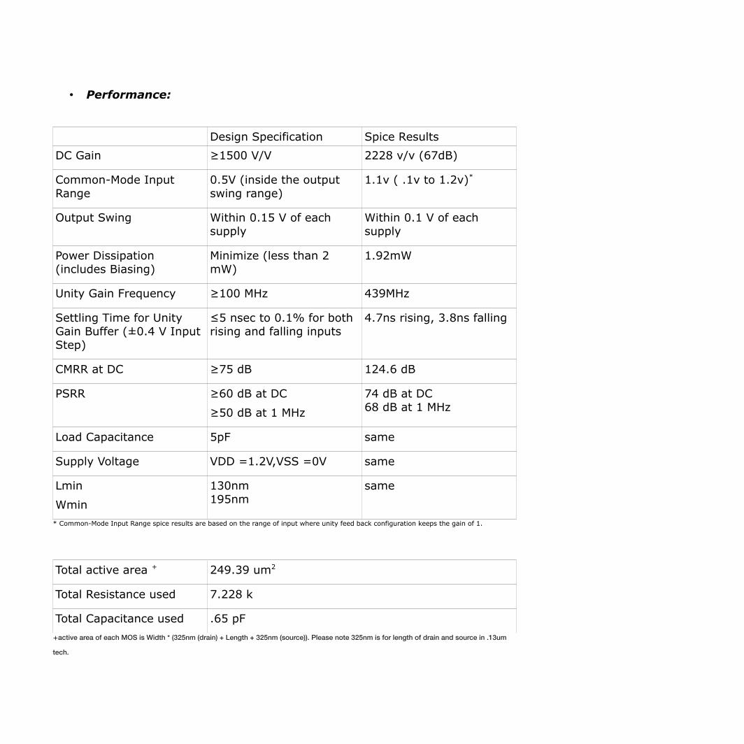
• Performance:
Design Specification Spice Results
DC Gain ≥1500 V/V 2228 v/v (67dB)
Common-Mode Input
Range
0.5V (inside the output
swing range)
1.1v ( .1v to 1.2v)*
Output Swing Within 0.15 V of each
supply
Within 0.1 V of each
supply
Power Dissipation
(includes Biasing)
Minimize (less than 2
mW)
1.92mW
Unity Gain Frequency ≥100 MHz 439MHz
Settling Time for Unity
Gain Buffer (±0.4 V Input
Step)
≤5 nsec to 0.1% for both
rising and falling inputs
4.7ns rising, 3.8ns falling
CMRR at DC ≥75 dB 124.6 dB
PSRR ≥60 dB at DC
≥50 dB at 1 MHz
74 dB at DC
68 dB at 1 MHz
Load Capacitance 5pF same
Supply Voltage VDD =1.2V,VSS =0V same
Lmin
Wmin
130nm
195nm
same
* Common-Mode Input Range spice results are based on the range of input where unity feed back configuration keeps the gain of 1.
Total active area +
249.39 um2
Total Resistance used 7.228 k
Total Capacitance used .65 pF
+active area of each MOS is Width * (325nm (drain) + Length + 325nm (source)). Please note 325nm is for length of drain and source in .13um
tech.
• Discussion:
In this section I will explain how I designed the op-amp to meet the spec
listed in Performance section. I also provide hspice wave plots showing the
results. This section is divided into subsections for each metric: 1. Open
Loop DC gain, 2. pole-zero calculations (phase response) 3. Slewing and
Settling time, 4. Bias circuit, 5. CMRR, 6. PSRR, 7. input CMR, and 8. output
swing.
1. Open Loop Differential Mode DC Gain:
Open Loop Different Mode DC Gain, Adm, is defined as:
Adm = vo/(inp - inn) = vo/vid = Adm_first_stage *
Adm_second_stage = gm1(ro2||ro4) * gm5(ro5||ro6)
where,
gm1 = 2I1/vov1 = I7/vov1
gm5 = 2I6/vov5
ro2 = 1/λ2I2=2/λ2I7
ro4 = 1/λ4I4=2/λ4I7
ro5 = 1/λ5I6
ro6 = 1/λ6I6
=> Adm = I7/vov1 * (2/I7 * 1/λ2||1/λ4) * 2I6/vov5 * (1/I6 * 1/λ6||
1/λ5)
canceling I6 and I7 above:
Adm = 4/(vov1*vov5) * 1/(λ2+λ4) * 1/(λ6+λ5) (1)
Due to design requirements as will be clear later in this section, vov1
was chosen as .124v, vov5 as .1v, L2-6 as Lmin ( λ4=λ5=.2v-1 and
λ6=λ2=.15v-1
).
Plugging numbers in (1), will give gain of 2632 v/v. Hspice simulation
has DC gain of 2228 v/v as depicted in picture-1 below.

Picture-1: Open Loop Differential Mode Gain
2. Pole and Zero Calculation:
There are three node that can have poles: output node, output of first
stage, and gate of current mirror load in first stage, node 3. First let's
see node 3 is a show stopper:
2.1 Pole at node 3:
I investigated possible pole frequency for the gate of current
mirror load, and found out that the pole associated there are too
fast to worry about. Here are the calculations:
C3=2/3W3L3Cox + 2/3W4L4Cox, where cox is eox/tox= 13.27 fF/um2.
Before I came up with final W and L values which are listed in the
table of Transistors Summary, I used smallest value for W and L,
190nm and 130nm respectively, and a typical value for 1/gm3 which
is the resistance seen by this cap, C3, .1k for 1mA current in M3 and
0.1v vov3. The value for pole frequency at this node came up to be
3.5THz. So, even making R and C associated for this pole 1000x
larger which is not the case here, this pole is out of range of our
operation, so it can be ignored. Simulation results later confirmed this
assumption.
2.2 Poles and zeros after compensation:
As depicted in the circuit digram, compensation cap Cc is used in
series with nulling resistor Rz, to move RHP zero created by Cc alone
to LHP and cancel wp2[4]. Poles and zeros in this circuit topology are
as follow:
To find ωp1:
ω p1 =1/(RI.gmII.RII.Cc)
where, RI is the output resistance of first stage: ro2||ro4,
gmII is the transconductance of second stage: gm5,
RII is the output resistance of second stage: ro5||ro6,
and, Cc is the compensation capacitance as depicted in the circuit.
ωp1 is also equal to gm1/(Adm.Cc) as Adm= gmI.RI.gmII.RII.
To find ωp2:
ω p2=gmII/CII
where CII is the output capacitance at output node, which is:
CII = CL + Cdb5 + Cdb6 + Cgd5 + Cgd6
After calculating typical values for Cdb and Cgd above I found that CII
is dominated by CL. The following show my calculations:
Cdb0 = CJ.AS + CJSW.PD + CJGATE.W
where, AS is 2HDIFF.W=2x130nmxW, and, PD is 4xHDIFF + 2W=
4x130nm+2W.
Putting values in the Cdb0 above for Wmin, we get:
Cdb0(Wmin)= 0.067fF, and this junction cap at 1v Vdb, decreases to:
Cdb(Wmin)|vdb=1v = Cdb0(Wmin)/ √1+1v /2φf = 0.041fF
For case of Cgd, we have:
Cgd = LD.W.Cox, and for Wmin Cgd(Wmin)=0.064fF
We can see from Cdb and Cgd values above, even for large size
transistors, they are much smaller than CL of 5pF.
To find ωp3:
ω p3= 1/RzCI,
where CI is the output capacitance of first stage before putting Cc in
the circuit.
CI = Cgd2 + Cdb2 + Cdb4 + Cgd4 + gm5RIICgd5 + Cgs5
When I was designing the circuit, I didn't have values for Ws in the
beginning, so I couldn't guess CI, but it can be seen from this
equation that CI should be small value, and with small value Rz, ωp3,
which will become the second pole of the system after pole-zero
cancellation of ωp2 and ωz, is very fast. This assumption turned out
to be true when I first simulated the circuit and found PM=90.
However, due to slow settling which I will explain later, PM became 75
degrees. And it seems ωp3 came into frequency range of circuit.
By plugging final design values to ωp3, I get:
Rz=228 ohm,
gm5= 25.6mS,
RII = 1/474uS = 2.1k,
Cgd5 = 18.2fF,
So, CI is around 1pF, and ωp3=1/228x1pF=4.4Grad/s, and
fp3=700MHz. For PM=75, we get unity gain frequency of
fu=tan(15).fp3=200MHz. fu I measured in spice was around 400MHz.
The followings are poles and zeros from hspice simulation:
fp1=-248.871k
fp2=-123.399x
fp3=-933.019x
fz= -146.884x
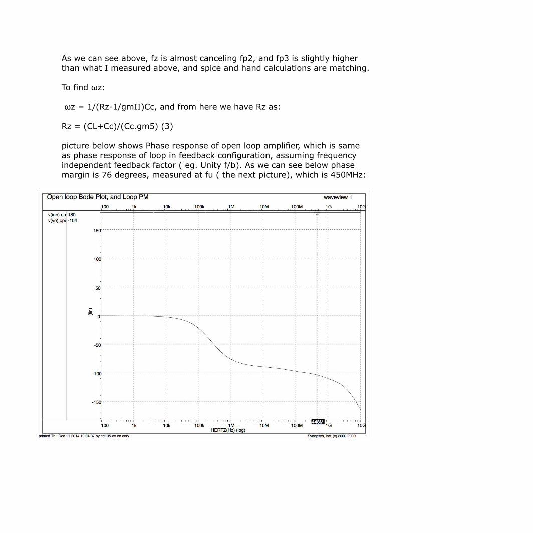
As we can see above, fz is almost canceling fp2, and fp3 is slightly higher
than what I measured above, and spice and hand calculations are matching.
To find ωz:
ω z = 1/(Rz-1/gmII)Cc, and from here we have Rz as:
Rz = (CL+Cc)/(Cc.gm5) (3)
picture below shows Phase response of open loop amplifier, which is same
as phase response of loop in feedback configuration, assuming frequency
independent feedback factor ( eg. Unity f/b). As we can see below phase
margin is 76 degrees, measured at fu ( the next picture), which is 450MHz:
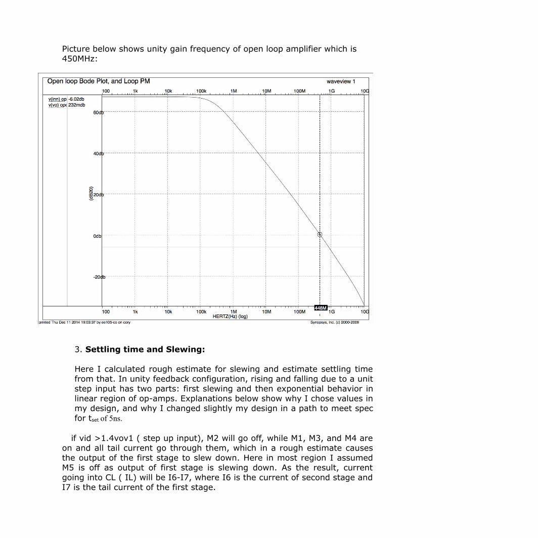
Picture below shows unity gain frequency of open loop amplifier which is
450MHz:
3. Settling time and Slewing:
Here I calculated rough estimate for slewing and estimate settling time
from that. In unity feedback configuration, rising and falling due to a unit
step input has two parts: first slewing and then exponential behavior in
linear region of op-amps. Explanations below show why I chose values in
my design, and why I changed slightly my design in a path to meet spec
for tset of 5ns.
if vid >1.4vov1 ( step up input), M2 will go off, while M1, M3, and M4 are
on and all tail current go through them, which in a rough estimate causes
the output of the first stage to slew down. Here in most region I assumed
M5 is off as output of first stage is slewing down. As the result, current
going into CL ( IL) will be I6-I7, where I6 is the current of second stage and
I7 is the tail current of the first stage.
So,I have, slew rate of CL as:
SR2=IL/CL = I6-I7/CL
I ignore slew down of CL as it should be fast due to M5 current large
while output of first stage is slewing up and causes vgs of M5 to be
large.
As Vid>1.4vov1, we slew, I should choose values for vov1 and vov2.
The larger this value, the less slewing I will have as vid-1.4vov1 is the
amount of dv for vo where we slew in unity feedback ( vid step is .4v
in this project). At the same time, Input Common Mode Range, CMR,
put an upper limit for vov1/vov2. As I used cascode in my tail of diff
pair and vod requirement of 0.1v in this project, if we set vov of M3
( current mirror load) to 0.1v, which is a good choice in terms of CMR
and as I explained before pole at gate of this current mirror load
doesn't affect our performance ( small vov3 and larger W3 is ok for
this node), and we put vod of 0.1v for cascode tail PMOS transistors,
input CMR becomes vdd-vov3-vov7-vov8-vT1-vov1-GND. This CMR
will be 1.2v-.1-.1-.1-.3-vov1>.5v. So vov1 shouldn't be more than
0.1v. Please note as input common mode comes lower toward gnd, VT
of M1-2 will be increased due to body effect ( .05v increase in this
technology), and this allow input common mode to come as low as
50mv instead of 100mv as explained above. However, spec says, CMR
of .5v inside output swing range. From here vov5 should be 0.1v. In
this design final vov1-2 I used was 124mv.
I want to have an idea how slewing will be:
dvo slews for amount of vid-1.4vov1 which from vov1 of .15v ( I
originally used this vov in my first iteration) and vid of .4v,
dvo=188mv ( vout slews for 188mv in 400mv step input).
SR2=188mv/dtSR2=I7/CL, where dtSR2 is the amount time it take for
output to slew into linear region ( vid becomes <1.4vov1).
To find dtSR2
I7=CLx188mv/dtSR2=940uA.ns
/ dtSR2, where 5pFx188mv=940uA.ns
Finally,
dtSR2 = 940uA.ns/I7 (2)
We have 5ns budget to go into .1% error bounds in .4v input step.
After slewing it takes 6.9�[5] to reach .1% error bound in one pole
response, where �=1/ωu, ( which is almost the case here), we have:
5ns - dtSR2 > 6.9�
from (2) above we have:
5ns - 940uA.ns
/I7 > 6.9/ωu
And we know from gain BW product that ωu=gm1/Cc, so:
5ns - 940uA.ns
/2I1 > 6.9Cc/gm1
And, gm1=2I1/vov1, so:
5ns – 940uA.ns
/2I1 > 6.9Cc.vov1/2I1
taking vov1=.15v, we have:
5ns > (940uA.ns + 6.9x.15vxCc)/2I1 (4)
Here to find a value for I1, I calculated Cc based on PM=60, as follow:
1.73xωu = ωp2, where ωp2 is gmII/CL. That is true that ωp2 will be
cancelled by ωz, but I chose as my starting point to find Cc. This
approach can help if we get a doublet in case not exact canceling of
pole and zero. So we have:
1.73ωu = gm5/CL
where ωu is gm1/Cc, so:
1.73x(gm1/Cc) = gm5/CL (a)
To have equal slew rate for outputs of first and second stage, we take
current in second stage twice the current in first stage ( I6=2I7=4I1)
[6], if CL=Cc.
With vov1=.15v, vov5=.1v, and I5=4I1, we have:
Cc=1.73xCLxgm1/gm5 = 1.44pF. ( Please note my final Cc is .65pF.
My final I5=8.2xI1, and vov1=.12v, and eguation (a) above gives Cc
of .8pF.)
With Cc=1.4p, from (4) above I get:
I1>245uA, and I6>980uA.
From equation (3):
Rz = I/gm5 x (CL+Cc)/Cc
with vov5=.1v and I5=I6=980uA, and Cc=1.44pF, we get:
Rz = 228ohm.
By these values I sized transistors, using square law equation to find
W/L ratio, and keeping L as Lmin to save area and less parasitic caps
( Please note per [7], Lmin is not optimum value for analog design
because of variation mismatches).
After simulating for first time, rising part of output for .4v step up
input, was 30-40% slower than 5ns settling time budget, where fall
down part was very fast. After discussion with GSI and Prof Allstot, I
increased current of second stage by 40%, and to keep circuit below
2mW budget, I decreased first stage current by some amount. To
keep ωu intact ( ωu=gm1/Cc), I decreased Cc, which matches my Cc
calculation above. Please note, these changes won't change gain due
to equation (1) or other metrics such as CMRR or PSRR which I will
explain later in this section. In my changing values, my PM was
decreased to 75degrees which is actually the optimum PM for .1%
error bound[3].
Please note, by paying attention to pole and zero locations explained
above, Rz seems to stay unchanged as:
Rz=1/gm5 * (CL+Cc)/Cc
and, as gm5 goes high due to I5 increase, and Cc goes low, Rz
shouldn't change that much which was the case for my design ( note
here CL>>Cc).
Also, ωp2=gm5/CL, and ωz=1/(Rz-1/gm5)Cc. ωp2 increases as I5
increases and ωz also increases as Cc decreases (As 1/gm5 is a
very small value even in compare to Rz) . So pole-zero cancellation is
still happening. This was verified by pole zero values I showed in my
hspice sim in section 2.2.
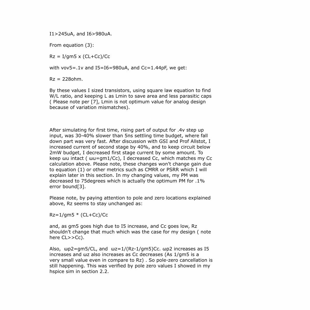
Below are waveview of settling time for vid=.4 step up at t=1ns,
and step down at t=14ns:
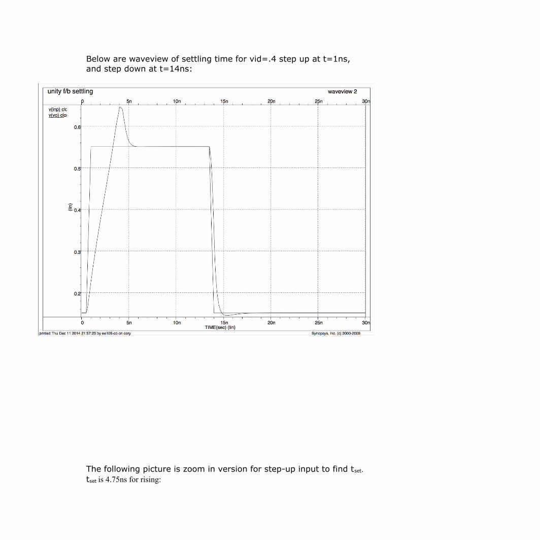
The following picture is zoom in version for step-up input to find tset.
tset is 4.75ns for rising:
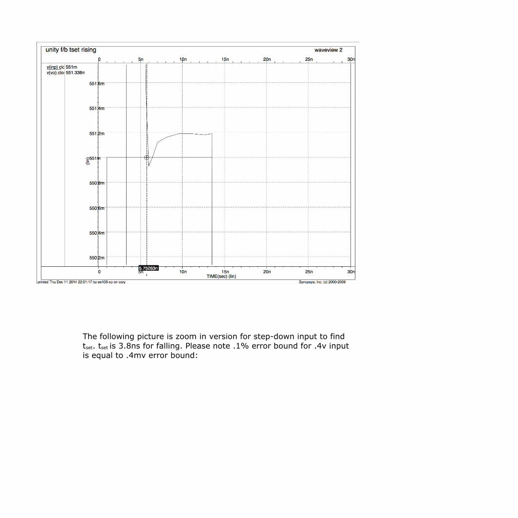
The following picture is zoom in version for step-down input to find
tset. tset is 3.8ns for falling. Please note .1% error bound for .4v input
is equal to .4mv error bound:
4. Bias Circuit:
I used Sooch circuit current mirror[2] in PMOS fashion to bias the tail
cascode of diff pair, with vov of 0.1v for each PMOS transistor in tail.
Below is picture of bias circuit repeated:

As a result of this gate of M9 should at vdd-vt-vov8=1.2v-.3v-.1=.8v,
and gate of M10 should be vdd-vov8-vov7-vt7, please note here vt7 is
slightly increased (10mv here) due to backgate effect. I chose
vg10=.68v.
To find value of RB and W/L ratios, I did as follow:
Let's name drain of M12 as VB. Equations for the current in saturated
transistor M12 and triode transistor M11 are as follow ( please note
VTP for M11 and M12 are increased due to backgate effect, and I
used value of .35v in my hand calculations). Also note that drain
of M9 should be at 1.1v to match M8:
I12=1/2K'p(W/L)12(.68v - .35v -VB)2
VDS11= VG9-VG10=.8v-.68=.12v
I11=K'p(W/L)11[(.8v-VB-.35v)x.12v -1/2(.12)2]
I11=I12, and by picking .1v for VB, and (W/L)11 Wmin and Lmin, we
get I11=14uA. Here I get RB=7k which are reasonable values for RB
and Ibias, so I stop at this point. M9 and M10 were sized accordingly.
Please note M9 and M10 are in saturation. In hspice actual current in
bias part is 11uA where the total current budget for 2mW design is
166uA.
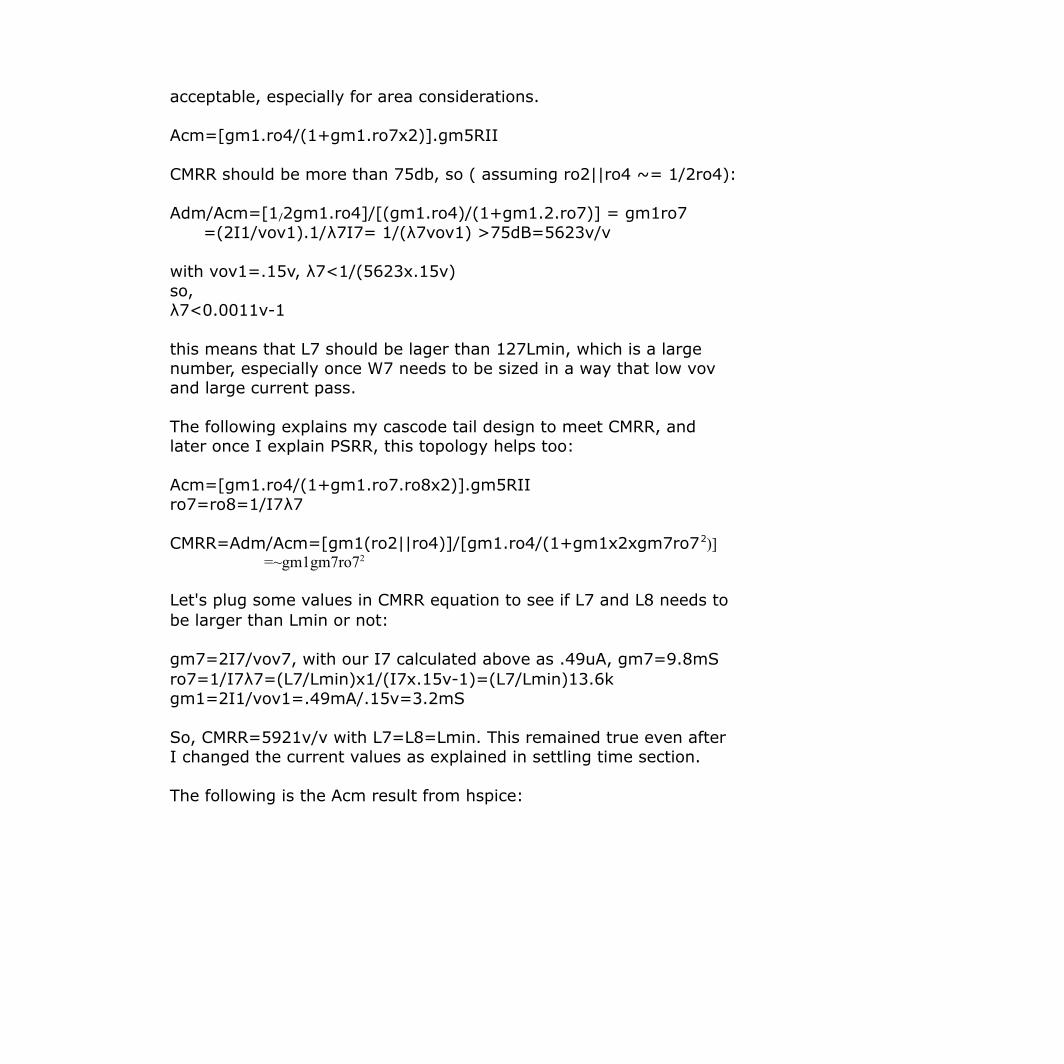
5. CMRR :
In the beginning I used a single transistor in the tail of diff pair,
however the following calculations show that that approach is not
acceptable, especially for area considerations.
Acm=[gm1.ro4/(1+gm1.ro7x2)].gm5RII
CMRR should be more than 75db, so ( assuming ro2||ro4 ~= 1/2ro4):
Adm/Acm=[1/2gm1.ro4]/[(gm1.ro4)/(1+gm1.2.ro7)] = gm1ro7
=(2I1/vov1).1/λ7I7= 1/(λ7vov1) >75dB=5623v/v
with vov1=.15v, λ7<1/(5623x.15v)
so,
λ7<0.0011v-1
this means that L7 should be lager than 127Lmin, which is a large
number, especially once W7 needs to be sized in a way that low vov
and large current pass.
The following explains my cascode tail design to meet CMRR, and
later once I explain PSRR, this topology helps too:
Acm=[gm1.ro4/(1+gm1.ro7.ro8x2)].gm5RII
ro7=ro8=1/I7λ7
CMRR=Adm/Acm=[gm1(ro2||ro4)]/[gm1.ro4/(1+gm1x2xgm7ro72)]
=~gm1gm7ro72
Let's plug some values in CMRR equation to see if L7 and L8 needs to
be larger than Lmin or not:
gm7=2I7/vov7, with our I7 calculated above as .49uA, gm7=9.8mS
ro7=1/I7λ7=(L7/Lmin)x1/(I7x.15v-1)=(L7/Lmin)13.6k
gm1=2I1/vov1=.49mA/.15v=3.2mS
So, CMRR=5921v/v with L7=L8=Lmin. This remained true even after
I changed the current values as explained in settling time section.
The following is the Acm result from hspice:
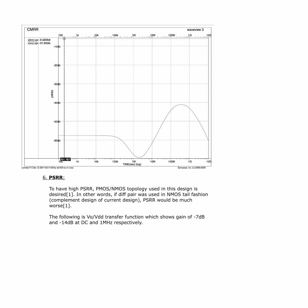
6. PSRR :
To have high PSRR, PMOS/NMOS topology used in this design is
desired[1]. In other words, if diff pair was used in NMOS tail fashion
(complement design of current design), PSRR would be much
worse[1].
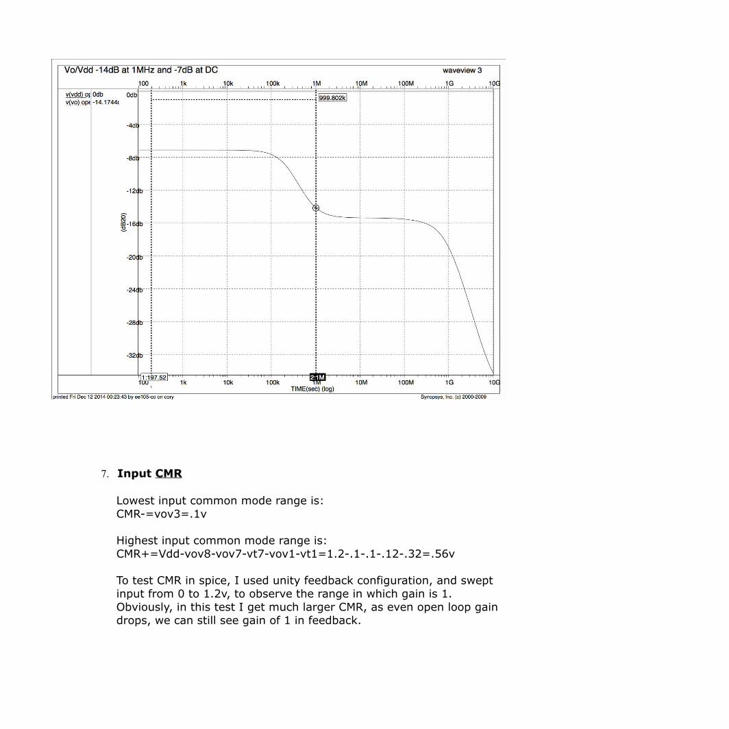
The following is Vo/Vdd transfer function which shows gain of -7dB
and -14dB at DC and 1MHz respectively.
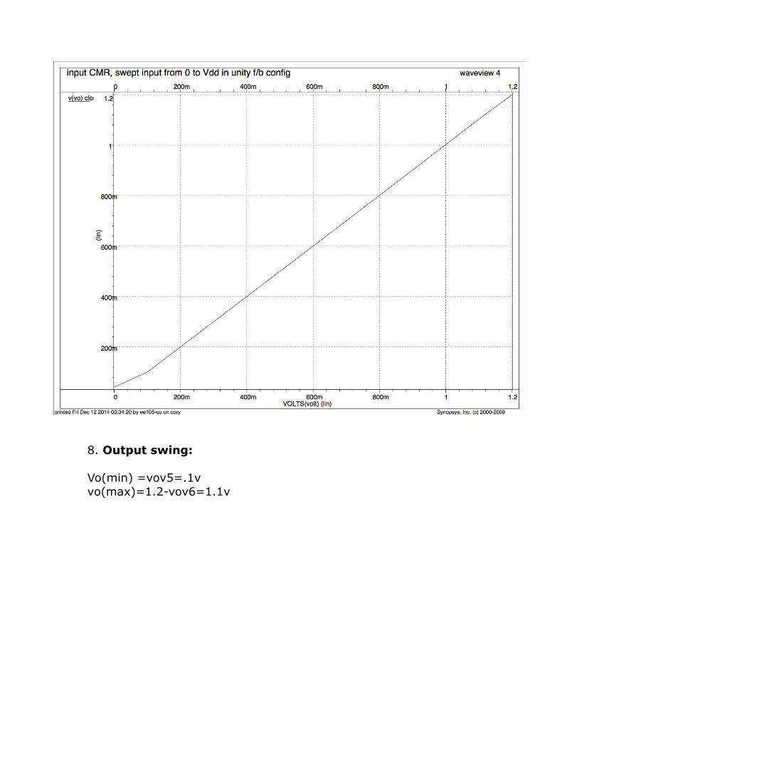
7. Input CMR
Lowest input common mode range is:
CMR-=vov3=.1v
Highest input common mode range is:
CMR+=Vdd-vov8-vov7-vt7-vov1-vt1=1.2-.1-.1-.12-.32=.56v
To test CMR in spice, I used unity feedback configuration, and swept
input from 0 to 1.2v, to observe the range in which gain is 1.
Obviously, in this test I get much larger CMR, as even open loop gain
drops, we can still see gain of 1 in feedback.
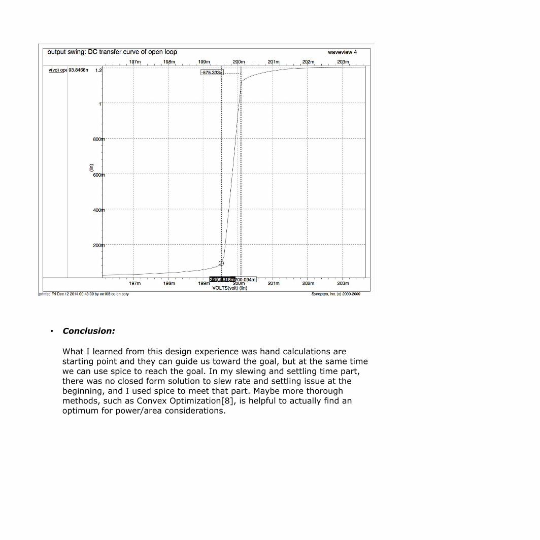
8. Output swing:
Vo(min) =vov5=.1v
vo(max)=1.2-vov6=1.1v
• Conclusion:
What I learned from this design experience was hand calculations are
starting point and they can guide us toward the goal, but at the same time
we can use spice to reach the goal. In my slewing and settling time part,
there was no closed form solution to slew rate and settling issue at the
beginning, and I used spice to meet that part. Maybe more thorough
methods, such as Convex Optimization[8], is helpful to actually find an
optimum for power/area considerations.
• References:
[1] P. Gray and R. Meyer “Analysis and Design of Analog Integrated Circuits 5th
ed.” section 6.3.6
[2] P. Gray and R. Meyer “Analysis and Design of Analog Integrated Circuits 5th
ed.” page 269
[3] H. Yang and D. Allstot "Considerations for fast settling operational amplifiers",
IEEE Trans. Circuits Syst., vol. 37, no. 3, pp.326 -334 1990
[4] P. Gray and R. Meyer “Analysis and Design of Analog Integrated Circuits 5th
ed.” section 9.4.3
[5] DJ Allstot “EE240A lecture notes at UC Berkeley, Fall 2014” pg. 125
[6] DJ Allstot “EE240A lecture notes at UC Berkeley, Fall 2014” pg. 169
[7] DJ Allstot “EE240A lecture notes at UC Berkeley, Fall 2014” pg. 64
[8] S. S. Mohan, M. del Mar Hershenson, S. P. Boyd, and T. H. Lee, "Simple
accurate expressions for planar spiral inductances", IEEE J. Solid-State Circuits,
vol. 34, pp.1419 -1424 1999