cmos limitation
TRANSCRIPT

Device Scaling Limits of Si MOSFETs and TheirApplication Dependencies
DAVID J. FRANK, MEMBER, IEEE, ROBERT H. DENNARD, FELLOW, IEEE,EDWARD NOWAK, MEMBER, IEEE, PAUL M. SOLOMON, FELLOW, IEEE, YUAN TAUR, FELLOW, IEEE,AND HON-SUM PHILIP WONG, FELLOW, IEEE
Invited Paper
This paper presents the current state of understanding of thefactors that limit the continued scaling of Si complementary metal-oxide-semiconductor (CMOS) technology and provides an analysisof the ways in which application-related considerations enter intothe determination of these limits. The physical origins of these limitsare primarily in the tunneling currents, which leak through the var-ious barriers in a MOS field-effect transistor (MOSFET) when itbecomes very small, and in the thermally generated subthresholdcurrents. The dependence of these leakages on MOSFET geometryand structure is discussed along with design criteria for minimizingshort-channel effects and other issues related to scaling. Scalinglimits due to these leakage currents arise from application con-straints related to power consumption and circuit functionality. Wedescribe how these constraints work out for some of the most impor-tant application classes: dynamic random access memory (DRAM),static random access memory (SRAM), low-power portable devices,and moderate and high-performance CMOS logic. As a summary,we provide a table of our estimates of the scaling limits for var-ious applications and device types. The end result is that there isno single end point for scaling, but that instead there are many endpoints, each optimally adapted to its particular applications.
Keywords—CMOS, device design, discrete dopants, double-gateMOSFET, DRAM, high-k dielectrics, high-performance logic,leakage currents, limits, low power, MOSFET, nanotechnology,power density, scale length, scaling, SRAM, tunneling.
I. INTRODUCTION
In 1930, Lilienfeld [1] patented the basic concept of thefield effect transistor (FET) . Thirty years later, in 1960, itwas finally reduced to practice in Si–SiOby Kahng and At-tala [2]. Since that time, it has been incorporated into inte-grated circuits and has grown to be the most important devicein the electronics industry. Progress in the field for at least the
Manuscript received March 30, 2000; revised September 26, 2000.The authors are with the IBM Thomas J. Watson Research Center,
Yorktown Heights, NY 10598 USA (e-mail: [email protected];[email protected]).
Publisher Item Identifier S 0018-9219(01)02066-7.
last 25 years has followed an exponential behavior that hascome to be known as Moore’s Law [3]. Since 1994, the semi-conductor industry has been projecting these exponentialsinto the future to provide technology development targets.The most recent of these projections is the 1999 InternationalTechnology Roadmap for Semiconductors (ITRS99) [4]. Itcontains projections for complementary metal-oxide-sesmi-conductor (CMOS) technology out to 2014, including 32-Gbdynamic random access memory (DRAM) entering produc-tion and processors with gate lengths down to 20 nm and2 10 FETs per chip.
But will these exponential projections come to pass orwill physical limits make them impossible? Many reviewshave been written about the current state and future prospectsfor Si MOS field-effect transistors (MOSFETs) and CMOSs[5]–[9]. In particular, many different scaling limits for MOS-FETs have been proposed and discussed. In this work, wedescribe the current state of understanding of these scalinglimits and seek to advance this state of understanding by ad-dressing the ways in which application requirements must beintertwined with the setting of limits. The result in the end isthat there will be no single “end to scaling,” but rather, a widerange of limiting FET technologies, each optimally adaptedto its applications.
Much of our discussion centers on bulk-like MOSFETscaling,asillustratedinFig.1,butthisisnotintendedtoexcludeother device geometries for MOSFETs. In particular, partiallydepletedsilicon-on-insulator(PD-SOI)MOSFETsareconsid-ered tobepartof thisbulk-likecategory,sincemostof thesamelimits apply to PD-SOIs as to bulk. Consequently, PD-SOIis not explicitly discussed except when there are significantdevice design differences. At the circuit level, there are, ofcourse, some important features of SOIs, such as the floatingbodyeffects,but thesearefor themostpartoutside thescopeofthispaper.Thescalingbehavioroffullydepletedsilicon-on-in-sulator (FD-SOI) MOSFETs depends a great deal on the
0018–9219/01$10.00 © 2001 IEEE
PROCEEDINGS OF THE IEEE, VOL. 89, NO. 3, MARCH 2001 259
thicknessof theburiedoxide.For thickburiedoxide, there isnobacksidescreeningofthedrainpotential,resultinginrelativelypoor scaling characteristics compared to other device types[10]–[13]. Since such devices are not likely to be used at thelimits of scaling they are not discussed here. We do, however,discuss the scaling advantages of the more novel double gatedtype of FD-SOI MOSFETs, wherein both the insulator on theback side of the Si channel layer and the Si layer itself are verythin so that both sides of the channel are gated. There are alsoin-betweenFD-SOI MOSFETs withburiedoxide thinenoughto offer some screening, but not thin enough for use in activeswitching.These devicesare interesting from a circuit point ofview since the back gate can be used to dynamically adjust thethresholdvoltage,butarenotdiscussedherefor lackofspace.
The outline of the paper is as follows. Section II ad-dresses some of the more fundamental limitations to thecontinued scaling of MOSFETs that appear to be on thehorizon. Based only on these fundamental limits, it maybe possible to scale FETs down to very small dimensions,e.g., 10-nm channel length or smaller. Section III describesresearch results related to this fundamental limit regime:very tiny one-of-a-kind FETs. In the more practical world ofmanufacturing, however, there are many types of variationsand fluctuations that require the design of MOSFETs withtolerances. In Section IV, we look at some of these practicallimitations and their consequences for device design. Sec-tion V describes how the concepts of the previous sectionsplay out when they are applied to meeting the needs ofspecific classes of applications. The paper ends in Section VIby summarizing all of the limits into a large table, followedby the conclusion in Section VII.
II. FUNDAMENTAL SCALING LIMITS
A. Scaling Theory
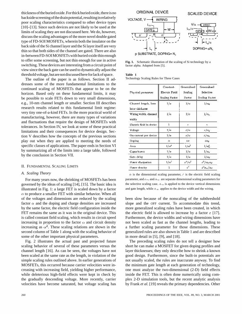
For many years now, the shrinking of MOSFETs has beengoverned by the ideas of scaling [14], [15]. The basic idea isillustrated in Fig. 1: a large FET is scaled down by a factor
to produce a smaller FET with similar behavior. When allof the voltages and dimensions are reduced by the scalingfactor and the doping and charge densities are increasedby the same factor, the electric field configuration inside theFET remains the same as it was in the original device. Thisis called constant field scaling, which results in circuit speedincreasing in proportion to the factor and circuit densityincreasing as . These scaling relations are shown in thesecond column of Table 1 along with the scaling behavior ofsome of the other important physical parameters.
Fig. 2 illustrates the actual past and projected futurescaling behavior of several of these parameters versus thechannel length [16]. As can be seen, the voltages have notbeen scaled at the same rate as the length, in violation of thesimple scaling rules outlined above. In earlier generations ofMOSFETs, this occurred because carrier velocities were in-creasing with increasing field, yielding higher performance,while deleterious high-field effects were kept in check bythe gradually descending voltage. More recently, carriervelocities have become saturated, but voltage scaling has
Fig. 1. Schematic illustration of the scaling of Si technology by afactor alpha. Adapted from [5].
Table 1Technology Scaling Rules for Three Cases
� is the dimensional scaling parameter," is the electric field scaling
parameter, and� and� are separate dimensional scaling parameters for
the selective scaling case.� is applied to the device vertical dimensions
and gate length, while� applies to the device width and the wiring.
been slow because of the nonscaling of the subthresholdslope and theOFF current. To accommodate this trend,more generalized scaling rules have been created, in whichthe electric field is allowed to increase by a factor[17].Furthermore, the device widths and wiring dimensions havenot been scaled as fast as the channel lengths, leading toa further scaling parameter for those dimensions. Thesegeneralized rules are also shown in Table 1 and are describedin more detail in [5], [9], and [18].
The preceding scaling rules do not tell a designer howshort he can make a MOSFET for given doping profiles andlayer thicknesses; they only describe how to shrink a knowngood design. Furthermore, since the built-in potentials arenot usually scaled, the rules are inaccurate anyway. To findthe minimum gate length at each generation of technology,one must analyze the two-dimensional (2-D) field effectsinside the FET. This is often done numerically using com-plex 2-D simulation tools, but the recent analytic analysisby Franket al. [19] reveals the primary dependencies. Other
260 PROCEEDINGS OF THE IEEE, VOL. 89, NO. 3, MARCH 2001

Fig. 2. Past and projected future scaling trends for CMOS logic.(a) Supply voltage and threshold voltage versus channel length. (b)Gate oxide thickness and 2-inNAND delay versus channel length.Adapted from [16].
(a)
(b)
Fig. 3. Idealized schematic cross section diagrams of (a) a bulkMOSFET and (b) a DG-FET, defining the insulator thicknesst andthe depleted Si thicknesst . � is the dielectric constant of siliconand � is the dielectric constant of the gate insulator(s). Adaptedfrom [19].
analyses have been made in the past [10], [20], [21], but weprefer this approach because it allows us to treat the high-dielectric case accurately.
According to this theory, the details of which are summa-rized in the Appendix, the potential variations in the channel
(a)
(b)
(c)
Fig. 4. 2-D potential perturbations in nFETs caused by a 20-mVvariation in the drain potential. (a) 2-D numeric simulation forrealistic doping profiles. (b) Simple analytic theory using the sameconditions as (a). (c) 2-D numeric simulation for a high-k gateinsulator (k = 78, 30 nm thick) with extreme ground-plane-likedoping profiles and shallow source and drain. From [33].
of an idealized MOSFET structure such as that in Fig. 3(a)can be expressed analytically using functions of the form
. The full dielectric boundaryconditions can be satisfied by matching these functions at theinterface, leading to an implicit equation for the scale length
, which characterizes the lowest order solution
(1)
where the symbols are defined in Fig. 3. In the mostcommon regime, and (1) can be approximatelysolved as
. There is also an analogous scale length forthe double-gate MOSFET (DG-FET), which is a three-layerstructure with a gate and a thin gate insulator on both sidesof the channel, as shown schematically in Fig. 3(b). Itsequation is given in the Appendix. Fig. 4(a) and (b) shows
FRANK et al.: DEVICE SCALING LIMITS OF Si MOSFETs AND THEIR APPLICATION DEPENDENCIES 261

Fig. 5. Plots of (a)�V , DIBL, and inverse subthreshold slopeand (b) transconductance (G ) and output conductance (G ), allversus theL=� ratio, showing the dependence of short channeleffects on channel length. Based on 2-D FIELDAY simulations ofidealized FET structures with� = 13:6 nm (t = 1:5 nm,t =10 nm).�V is determined atV = 0:05 V, DIBL is definedasV (V = 0:05) � V (V = 1:0), the transconductanceis measured atV = 1:0 V, V = V (V = 0:05) + 0:5V and the output conductance is measured at the sameV , andV = 0:75 V.
a comparison between the numerically calculated 2-Dpotential change in a conventional MOSFET due to a changein drain voltage and the first-order analytic approximation.Clearly, the simple approximation accurately captures thefunctional form of the potential variation along the channel,where it is most important. The only substantial differenceis in the deep depletion under the drain, but this does notsignificantly influence the subthreshold behavior.
For this lowest order solution, the source–drain compo-nent of the potential in the center of the channel varies as
, where andare bias dependent. Since this gives a length dependence of
, the ratio is a fundamental measureof the quality of the FET. For , the FET will be-have nearly ideally according to the one-dimensional (1-D)gradual channel approximation, but for small therewill be strong 2-D effects, including drain-induced barrierlowering (DIBL), high-output conductance, and rolloff.The dependence of these effects on is shown in Fig. 5for a particular case using 2-D numerical simulations of FETswith idealized doping profiles like those in Fig. 3(a). Evi-dently, is a fundamental limit on MOSFET as-pect ratio for this idealized design since voltage gain, givenby , needs to be greater than one for CMOS logic[22].
This scale length thus transforms the minimum gate lengthquestion into a question of maximum tolerable 2-D effects.From an idealized theoretical point of view, these effects canbe large and down to around one can be considered, as
Fig. 6. Plot of constant� contours versust andt for � =� =3. From Franket al. [19].
discussed in Section III. For current manufacturing toleranceratios and circuit design techniques, however, it appears thatthe minimum practical worst case short FETs have
(for DIBL 150 mV), so that the minimum practicalnominal design point is around , allowingfor 20% gate length variation. This is only possible be-cause the rolloff in bulk MOSFETs is partially compen-sated by lateral doping nonuniformity (e.g., halo doping, seeSection IV-A). For uniform lateral doping (e.g., an undopedDG-FET), it is probably necessary to havejust to keep below mV, although the exact ratioprobably depends on the desired . The bulk limit can beseen, for example, in recent manufacturing technology [23]in which the minimum gate length (100 nm) FETs have DIBLof 120 mV (at V) and of 10, whichcorrespond well to the point in Fig. 5. High
threshold rolloff at this point would be unacceptablyhigh, except that it is largely canceled out by careful halodoping.
As a specific example of this scale length, Fig. 6 shows thenumerically evaluated dependence offrom (1) on and
for the Si–SiO system. The simple linear approximationcorresponds well to the nm
case in Fig. 6, but note that the slope of the contours in-creases dramatically for shorter scale lengths, indicating asignificant departure from this approximate solution. Thisincreased slope is beneficial to highly scaled FETs since itimplies that the penalty for using insufficiently scaled oxidethickness is less than might have been expected.
By their nature, none of these scaling rules contain intheir formulation any limit on how far they can be applied.The limits enter due to physical phenomena that are notincluded in the scaling. The physical dimensions are lim-ited by quantum mechanical tunneling currents that passthrough the various barriers in the MOSFET when they aresufficiently thin, degrading the device’s behavior. Voltagescaling is limited on several fronts. The built-in junctionvoltages are set by the 1.1-eV bandgap of Si which doesnot scale. Consequently, as the applied voltages are scaleddown toward 1 V, the internal fields do not automaticallyscale as desired. A similar difficulty occurs in trying to scale
262 PROCEEDINGS OF THE IEEE, VOL. 89, NO. 3, MARCH 2001

Fig. 7. Calculated (lines) and experimental (dots) results for tunnelcurrents from inversion layers through thin oxides. Adapted from Loet al. [24].
the threshold voltage , which is tied to the nonscalingbehavior of the subthreshold slope and its influence onthe OFF current. At very low values, the supply voltageis also fundamentally limited by the need for sufficientgain to provide logic functionality. These and other issuesassociated with scaling are examined in more detail below.Currently, the scaling of physical dimensions is also limitedin a practical sense by the discreteness of dopants sincepresent manufacturing techniques do not control the exactplacement of dopant atoms. Consequently, since very smalldevice volumes contain only a small number of dopants,large statistical variations become likely. Although singledevices can be built, large functional circuits may be unman-ufacturable by present techniques. This effect is discussedin Section IV-C.
B. Tunneling Limits
Tunneling current through the gate insulator is one of themost constraining limits to scaling. For SiO, the conven-tional gate insulator, this leakage (see Fig. 7) exceeds therequirements of some applications (e.g., DRAM) already at2.5–3 nm, even though high-performance logic technology iscurrently pushing 2-nm oxide thickness [23] to achieve thedesired performance. According to Fig. 7 [24], 2-nm SiOwill have a leakage current of about 0.1 A/cmat 1.2 V.For conventional designs this will only contribute a few mil-liwatts to the overall chip dissipation, which is only prob-lematic for very low power applications, but is indicativeof where things are headed. Several writers suggest that theupper limit of acceptable gate leakage is in the 1–10-A/cmrange [25]–[27] or even 100 A/cm[28], although if one as-sumes more aggressively that up to 10% of the total powerdissipation could be due to gate leakage (see Section V-A),then it may be possible to tolerate leakage1000 A/cm invery high performance chips and even higher densities insmall areas (unless reliability problems prevent it, see Sec-tion V-A). Either way, the minimum pure SiOgate insu-lator thickness for high-performance applications is in the
1.0–1.5-nm range, which should be reached in one or twogenerations. Lower power applications require thicker min-imum oxide thickness and are already near their limits.
What can be done to circumvent this limit? There are atleast three paths of attack, all of which may be useful. Thefirst approach is to stop scaling the oxide, but attempt tocontinue scaling the rest of the FET in such a manner as tocompensate for the thicker oxide. A related approach is tochange the device structure in such a way that the MOSFETcan be scaled further, even with the relatively thicker oxide.DG-FETs are an example of this approach. The third ap-proach is to try to change the gate insulator to another ma-terial such that the effective capacitive thickness can be re-duced without increasing the tunneling current.
The first approach has two aspects: 1) one can reduce thedepletion depth (or the Si layer thickness for DG-FETs) asfar as possible, to minimize without further thinning ofthe oxide and 2) one can seek ways to reduce the minimumacceptable , such as improving the halo doping. The de-pletion depth can be reduced by increasing the doping and/orby forward biasing the body-source junction, but this hastwo drawbacks: body leakage currents and a degraded ide-ality factor. The leakage currents are due to forward body-source junction current and band-to-band tunneling betweenthe body and drain, which is described below. The idealityfactor is the reciprocal of the rate of change of the channelsurface potential as a function of (in the subthresholdregime) and is approximately equal to forbulk MOSFETs. It enters into the subthreshold slope, thusimpacting theOFF current. Applications that can be refrig-erated may particularly benefit in this regime, since forwardjunction current and degraded subthreshold slope can bothbe ameliorated by running at low operating temperature.
As mentioned briefly in the preceding section, a laterallynonuniform doping distribution can at least partially com-pensate for the rolloff that occurs for . Ofall the 2-D effects, rolloff has the worst effect on cir-cuit margins, so this compensation is very important andenables worst case to be reduced from 1.5 for nocompensation to 1.2 for current generation halo doping.Halo doping achieves this lateral nonuniformity by anglingin shallow body-type doping from the source and drain endsof the FET with the gate as a mask creating a “halo” aroundthe source and drain. For shorter FETs, these halo profileswork to create a higher average doping in the channel than isseen by a longer channel FET, thus tending to raise theinopposition to short-channel effects that are lowering it. Suchhalos are used to achieve the 25-nm bulk CMOS design de-scribed in Section IV-A. The other 2-D effects, however, arenot compensated and for much below 1.2, device per-formance becomes severely impacted anyway.
The second approach involves changing the devicestructure to one in which the gate essentially surroundsthe channel. The most investigated form is the DG-FET inwhich there are a gate and a thin gate insulator on both sidesof the channel, as shown schematically in Fig. 3(b). Thisgeometry has been shown to have better scaling propertiesthan the conventional bulk MOSFET [11], [12], [29] at least
FRANK et al.: DEVICE SCALING LIMITS OF Si MOSFETs AND THEIR APPLICATION DEPENDENCIES 263

for room temperature operation and is described in somedetail in Section IV-B. The three-dimensional (3-D) versionof these devices in which the channel is a thin post and thegate wraps around it cylindrically has the best electrostaticscaling properties of all and has been investigated by severalgroups [30], [31], but may prove to be impractical because ofthe high quantization energy levels for such a channel. (Thelowest quantum energy level of the confined channel adds tothe classical of the MOSFET, creating an additionalcontrol issue [6].) The primary advantages of these alternatedevice structures are a better ideality factor, near unity, andthe possibility of thinner Si channels than would be possiblein bulk devices except at very low temperature. It is not yetknown to what extent rolloff can be compensated inthese structures, although it seems that at least in principle,it may be possible to do so. For planar forms of the device,one could implant halo doping profiles into the channelalthough this would be subject to more fluctuations than forbulk devices because the volume available for such doping issmaller due to the thinness of the channel. Lateral variationsin the gate workfunction might also be possible [32].
Finally, there is much work aimed at reducing the gate tun-neling problem by changing to a higher permittivity () gateinsulator. This is largely a materials problem since its successdepends upon achieving high layer uniformity, integrationwith other Si processes, minimal/controlled reactions withSi and the gate electrode, and low fixed-charge, defect, andtrap densities in the insulator and at the interface between theinsulator and the Si substrate. Interface chemistry might alsonecessitate the use of metallic gate electrodes in which casemetals must be found with workfunctions near those of n-and p-poly-Si to achieve low s. If a suitable insulator canbe found, it would be characterized by three thicknesses: itsphysical thickness , its equivalent oxide tunneling thick-ness , and its equivalent oxide capacitive thickness
. Although would be larger than the (applicationdependent) minimum SiOfilm thickness for most high-dielectrics, the goal is to find an insulator with the propertythat when its is equal to the minimum SiOthickness,its is significantly less than the minimum SiOthick-ness. This would enable further scaling since when the gateinsulator permittivity varies, at least initially, all of the otherdevice dimensions and voltages can be scaled in keeping with
rather than the physical thickness(since this main-tains the scaling of charge density).
There are, however, some constraints on high-insulators.The scale length theory of Section II-A shows that the phys-ical thickness of the high-insulator becomes important as
increases, increasing the scale length and the drain poten-tial penetration under the gate [19], [33]. This is illustratedin Fig. 4(c), which shows the potential perturbation in thechannel of a MOSFET with gate insulator and thesame as in (a) and (b). Note that the potential fallsmuch more slowly in (c) than in (a) and (b), even thoughthe channel is longer in (c). A more detailed analysis offrom (1) shows that the physical insulator thickness shouldalways be less than the Si depletion depth under the channelsince otherwise the scale length will actually increase with
Fig. 8. Contours of constant scale length versus dielectric constantand insulator thickness, showing the useful design space for high-k
gate dielectrics. Data points are rough estimates of the tunnelingconstraints for various high-k insulators. Depletion depth is 15 nmhere. Useful design space will shrink with decreasing depletiondepth. From [33].
increasing [19]. This may be thought of as a case of “ma-jority rule”: when there is more insulator than Si, one ap-proaches the situation in which , i.e.,the Si gets converted to equivalent insulator thickness ratherthan the insulator being converted to equivalent Si.
The overall implications of the scale length considerationson high- dielectrics are illustrated in Fig. 8, which indicatesthe regime in which these dielectrics can usefully contributeto further scaling of Si MOSFETs. The contours of constant
are equivalent to contours of minimum gate length sinceminimum gate length is proportional to . Since it is unde-sirable to retreat from scaling and be forced to make largerFETs, the upper region that corresponds to larger minimumFETs than can be achieved with Si–SiOis blocked out. Thelower region is blocked out by the approximate tunnelingleakage limits of high- materials and reflects the empiricalobservation that insulator bandgaps tends to decrease withincreasing . Only the unhatched region is usefully availablefor high- improvements to scaling. Based on the ratio be-tween for SiO (19 nm) and the best accessibleat high
(15.5 nm), it appears that high-materials can offer aboutone additional generation of gate length scaling at fixed,but probably not more.
The gate insulator is not the only barrier through whichtunneling currents may flow in very small MOSFETs.The body-to-drain junction can also experience tunnelingcurrents if the field is high enough. Fig. 9 shows the fielddependence of such band-to-band tunneling currents. Sincethe cross-sectional area of the highest field body-to-drainjunction region is 1/3 that of the gate insulator, it may bepossible to tolerate higher tunneling current density, perhapsup to 3000 A/cm for aggressive high-end applications. Ac-cording to Fig. 9, this puts the scaling limit for body-to-drainelectric field at 2.7 MV/cm, which corresponds to peakbody doping around 310 cm for bulk MOSFETs,depending on bias and doping gradients, for a minimumdepletion depth of 8–13 nm. For low-power applications,the limit is likely to be below 1 A/cm or 1.7 MV/cm and0.8–1.2 10 cm body doping for a minimum of
264 PROCEEDINGS OF THE IEEE, VOL. 89, NO. 3, MARCH 2001

Fig. 9. Plot of band-to-band pn junction tunneling current versuselectric field for 1 V reverse bias. Adapted from [27].
13–15 nm. In SOI MOSFETs with floating bodies, includingDG-FETs, this tunneling current is potentially more prob-lematic because, in addition to creating dissipation, it cancharge up the floating body, lowering the effective thresholdvoltage. This body charging reaches steady state when thebody voltage is low enough that the thermionic current intothe source balances out the tunneling injection from thedrain. Since the tunneling current depends strongly on thedrain-to-source voltage, so does the body bias, which cancreate very high output conductance. For DG-FETs, the sit-uation is not quite so bad: the rate at which carriers that havetunneled from the drain into the body can thermionically exitthe body into the source is approximately the same as therate at which carriers are thermally injected into the channelfrom the source. Therefore, as long as the drain-to-bodytunneling current does not exceed the subthreshold channelcurrent, the device should behave reasonably well. For moreconventional SOI FETs, however, the barrier for carriersto leave the body can be much higher than the channelbarrier and therefore very little drain-to-body tunnelingcan be tolerated before the is shifted significantly. Theonly apparent way around this floating body problem forFD-SOI is to lower the supply voltage so that there is nodirect tunneling path available between drain and body. Thisimposes an approximate constraint on for conventionalFD-SOI of the form . For PD-SOI,there is also a second solution available: use a body contact.
It must be pointed out that these tunneling estimates couldeasily be too optimistic because the currents in Fig. 9 are forideal band-to-band tunneling. Such tunneling can be greatlyenhanced by deep traps in the junction, resulting in muchhigher junction leakage currents that would depend on thestatistical distribution of deep traps in the junctions. Thisproblem particularly impacts DRAM retention time distribu-tions [34], [35].
For verysmall MOSFETs, direct subthreshold source-to-drain tunneling through the potential barrier below the gateis another possible source of leakage current. This effect hasbeen reported in electrically variable shallow junction MOS-FETs (EJ-MOSFETs) operating at 77 K with physical gatelengths of 8 nm [36] and is expected to become important
at room temperature for channel lengths around 10 nm (seeSection III). It currently appears that scaling for most appli-cations will stop due to minimum insulator thickness prob-lems before this source-to-drain tunneling limit is reached.
One last tunneling-related constraint on scaling MOSFETsis tied to the need for FETs in most applications to providegreater than unity power gain, not to mention voltage gain.For sufficiently leaky gate insulators, the power required todrive the input leakage current could exceed the power avail-able at the output especially if the output conductance is high.This would turn the FET into an attenuator rather than an am-plifier and so represents perhaps the ultimate limit on thin-ning the gate insulator. For practical very large scale integra-tion (VLSI) applications, however, power density problemsare likely to limit scaling long before this limit is reached.
C. Voltage Limits
The most conspicuous nonscaling voltage in the conven-tional Si MOSFET is the Si bandgap potential V(where is the elementary charge), which can only bechanged significantly by changing the semiconductor itself.This nonscaling behavior does not actually limit operatingvoltage, but it does complicate device design. In traditionalcircuit design, the body is tied to the source supply voltageand, consequently, as the supply voltage is scaled downinto the 1-V range, the effect of the bandgap potential isincreasing. The primary effect is to increase the junctionfields and/or depletion depths in the FET above whatthey would be for ideal scaling. For the body-to-sourceand -drain junctions, the higher field necessitates higherjunction doping, but the nonscaled tends to suppress theband-to-band tunneling compared to what it would be if thebandgap were scaled. For the channel depletion region, theincreasing field perpendicular to the oxide interface con-fines channel carriers closer to the interface, reduces theirmobility, increases their quantum confinement energy, andincreases gate depletion. Since these effects tend to increasethe threshold voltage, they make it very hard to lowerto the levels needed for high-performance applications. Thefirst step in achieving a lower and channel surface fieldwhile still getting a scaled shallow depletion depth is to useretrograde doping profiles with low doping at the surface andhigh doping near the desired depletion depth [6]. If this doesnot lower sufficiently for some applications, one couldconsider very shallow counterdoping of the surface of theretrograde-doped channel to further lower the withoutsignificantly increasing the depletion depth. Alternately,most of these scaling problems can be addressed by for-ward biasing the body relative to the source [37] in a mannerwhich in effect scales . The problems with forwardbiasing the body include the need to generate and distributemore supply voltages and the forward-biased diode current,which would add to dissipation. Since the latter problemmight be solved by low-temperature operation, forward bodybias may indeed be a viable solution for high-performancecomputing applications and is discussed more extensively inSection IV-A. Note that PD-SOI MOSFETs tend to acquire
FRANK et al.: DEVICE SCALING LIMITS OF Si MOSFETs AND THEIR APPLICATION DEPENDENCIES 265

moderate forward body bias automatically in the processof equalizing the impact ionization and tunneling currentsentering and leaving the body.
The biggest limit to scaling is that theOFFcurrentof the FET is constrained by application considerations and
, where is the inverse subthresholdslope and is the current at which is defined. Since
, where is the ideality, is Boltzmann’sconstant, and is the temperature, the only way to scale
without also changing is to scale . For high-endapplications, this is beginning to happen to some extent,but for many applications (e.g., cell phones), significantcooling is not an option. For these low-to-moderate powerapplications, the maximum dissipation-limited active-mode
may range between 10 and 10 A/cm, resultingin minimum s varying between 0.54 and 0.27 V, re-spectively. These thresholds assume A/cm and
mV/decade. Very high-performance circuits mighttolerate thresholds near 100 mV (by this definition).Note that these are worst case thresholds at high .Nominal threshold voltages must be set higher to allowfor manufacturing tolerances. As noted before, double-gatestructures generally have smaller inverse subthreshold slope,perhaps 70 mV/decade at room temperature, allowing thethreshold and, hence, the supply voltage to be scaled further.
For very low-power applications, there is an interest in re-ducing the supply voltage as far as possible as a way of re-ducing the power by trading off performance [38]. From afundamental point of view, in binary digital logic, the min-imum permissible logic swing is the smallest swing that isstill large enough to maintain two distinct logic states andit was shown long ago that this level is around [22].This estimate can be refined by considering the self consis-tency required for a combinatorial logic gate. In this regime,each logic state is identified with a relatively small range ofvoltages, either high or low. Self consistency means that acombinatorial logic gate with any possible combination ofinputs taken from the logic state ranges will always producean output state that lies in one of the logic state ranges.
Conventional combinatorial logic circuits are built usingseries and/or parallel combinations of input devices, one (ortwo for CMOS) device(s) for each input. To find the fun-damental limits, imagine circuits in which the usual sourcesof logic state degradation (noise) are absent: there are novoltage drops in the wiring, no capacitive coupling betweenwires, no process-induced parameter variations among thedevices, no variations in the supply voltages, no extrinsicresistances, and no thermal noise. The nonlinearity of theactive devices serves to compress the variety of input logicstates into just two output states, but since the devices arenot “infinitely nonlinear,” a finite voltage range is required toachieve adequate compression. As an example, Fig. 10 illus-trates this for a simple CMOS four-inputNAND gate, where(a) shows the bias conditions which lead to the upper andlower logic state ranges. In Fig. 10(b), the logic swing is“large”; the “eye” diagram shows a small amount of noisemargin between the earliest switching gate with only oneinput changing and the latest switching gate with all of its in-
Fig. 10. Illustration of minimum swing determination usingideal four-input CMOSNAND gates. (a) Set of schematics definingconditions for best- and worst case logic outputs. (b)–(d) Transfercharacteristics in the form of “eye” diagrams. Output voltageversus input voltage and input voltage versus output voltage for thecases when only one input is switching and when all four inputsare switching. Inputs that are not switching are held atV . (b)Logic swing is above the minimum. Self-consistent low outputstates are betweenV andV and self-consistent high outputstates are betweenV andV . (c) Logic swing is exactly atminimum. (d) Logic swing is below the minimum; there are no fullyself-consistent output logic states.
puts changing and the output state ranges are isolated and selfconsistent, even though the range of input states does createsome spread. This logic swing is above the minimum limit.When the logic swing is reduced too far [see Fig. 10(d)], theearliest and latest curves no longer cross, indicating that thereis no self-consistent solution for and (as defined inthe figure). The lack of a self-consistent state means that op-erating a long chain of such logic gates can result in the lossof the logic signal (Fig. 11). Fig. 10(c) shows the minimumlogic swing condition: the earliest and latest curves are ex-actly tangent at their intersection points (and the noise marginis reduced to zero).
Using this type of minimum logic swing condition, analo-gous curves can be found for other logic families and fan-insand analytic calculations and simple circuit simulations canbe carried out to determine the minimum logic swing orsupply voltage; some results for MOSFETs are given in
266 PROCEEDINGS OF THE IEEE, VOL. 89, NO. 3, MARCH 2001

Fig. 11. Output signal versus time for every second gate in a serieschain of subthreshold CMOS four-inputNAND gates when operatedwith logic swing of 2:99�kT , which is below the minimum(3:01�kT ). Logic gates are configured in worst case fashion:low-going stages receive all four inputs from the previous stage,while high-going stages receive only one input from the previousstage, having the other inputs tied high. Note that for this case thelogic signal is lost after 35 stages.
Table 2Minimum Self-Consistent Supply Voltage for Fixed Fan-In LogicGates for Several Circuits and Conditions
Minimum design points assume that the device sizes and/or bias voltages
have been optimized to center the input/output curves. For random logic, the
minimum logic swing would be determined by the average or typical fan-in
rather than by the worst case, since high fan-in gates would be buffered by
lower fan-in circuits.
Table 2. These limits vary roughly as forconventional devices in their exponential regime, where
is the fan-in. Note that the lowest voltage FET resultsare achieved by using the FETs in their subthresholdregime, where they present their maximum exponentialnonlinearity. To achieve smaller minimum logic swing,one would need devices with stronger nonlinearities sincethe greater the nonlinearity, the smaller the voltage rangerequired for logic state compression. Using MOSFETs inthe conventional above-threshold manner decreases theiroverall nonlinearity and increases the required minimumsupply voltage, as shown in Fig. 12, from 75 mV ( )for pure subthreshold CMOS to 207 mV forat 300 K. Adding more contact resistance may also increasethe minimum supply voltage since it decreases overallnonlinearity[39]. Another consideration is that transientsimulations show increased timing variability (dependenceon input state) near the minimum logic swing limit becauseof the asymmetric switching.
Fig. 12. Minimum supply voltage versusV as a fraction ofV for four-input CMOSNAND gates. These calculations use aconstant mobility Brews model [97] to simulate 1.0-�m channellength surface channel FETs with thin oxide (4.5 nm) and realisticsource–drain contact resistances. Threshold voltage here is definedby the extrapolation to zero of the source–drain conductance forvery low drain voltages.
The introduction of realistic nonidealities such as noise,tolerances, and short-channel MOSFET behavior into theabove analysis will create a statistical spread of scenarios re-quiring higher voltages to guarantee logic state consistency.On the other hand, from a theoretical but impractical pointof view, one could buffer the output of every multiple inputlogic gate with a chain of inverters, effectively increasingthe gain and decreasing the minimum required supplyvoltage somewhat, although the power consumed by thebuffers seems likely to eliminate any real advantage fromthis approach.
D. Resistance Issues
It is implicitly assumed in the scaling theories that theparasitic resistance in series with the intrinsic MOSFETis either negligible or scalable along with the channelresistance. Otherwise, the performance gains derived fromscaling are quickly lost. For example, recent experimentalwork on 20-nm gate length MOSFETs reported currentlevels much below today’s optimized 100-nm devicesbecause of excessive series resistance [40].
In spite of this case, series resistance is not expectedto impose a fundamental limit on CMOS scaling. Tech-nological advances, e.g., self-aligned silicide for contactresistance reduction and rapid thermal annealing for abruptsource–drain formation, allow today’s state-of-the-arthigh-performance bulk nMOSFETs to achieve a seriesresistance below 100 m [23]. This is less than 10% of theeffective device resistance m.Ultimately, the intrinsic device resistance of an ideal ballisticMOSFET approaches , where is the effectivegate capacitance per unit area including quantum effects and
is the thermal injection velocity at the source [41]. For aphysical or equivalent of 1.0 nm, the limiting intrinsicdevice resistance is about 500 m. Even without furtherreduction in series resistance below currently achievedvalues, no serious performance degradation is expected.
For bulk CMOSs, there is a tendency for the series resis-tance to increase as the junction depth is scaled down for
FRANK et al.: DEVICE SCALING LIMITS OF Si MOSFETs AND THEIR APPLICATION DEPENDENCIES 267

shorter channel devices. But this is unlikely to pose a fun-damental problem as it can be dealt with by structural solu-tions such as raised source–drain using selective epi. Further-more, it is shown in Section IV-A that for an optimized halodesign, strict junction depth scaling is not required for shortchannel control. This can be understood from the principleof the scale length model in which the source–drain depthonly enters the preexponential factor of the threshold voltagerolloff.
Particular attention is needed to avoid high series resis-tance in SOI and/or DG-FETs that use thin silicon films.Ideally, the source and drain regions should fan out to amuch thicker film for reduction of both the electrical and thethermal resistance.
III. U LTIMATE MOSFETS
As indicated in the discussion about scale length and min-imum channel length in Section II-A, the primary constrainton shrinking channel length is the coupling between 2-Dshort channel effects and tolerances. When 2-D effects be-come large at very short channel length, random variationsin gate length, dopant positions, and other structural param-eters cause very large changes in device characteristics. Ifone is only interested in a single FET or if one assumes thatways can eventually be found to reduce process variationsto insignificance and to place dopants exactly, then toler-ances are not an issue and one can design and build extremelyshort gate-length MOSFETs. These can be very useful for ex-ploring the physics of small FETs even if they do not reflectmanufacturable processes.
The smallest reported experimental FETs are 8-nmEJ-MOSFETs made by Kawauraet al. [36]. As shown inthe cross-sectional diagram in Fig. 13(a), these electricallyvariable shallow junction nMOSFETs use a second gateover the top of the first gate to induce inversion layers in thesource and drain regions. Such inversion layers are muchshallower than the usual implanted source–drain extensions,which reduces to a minimum the influence of the drain onthe channel of the FET. The lower gates were patterned bye-beam lithography and lateral etching to achieve a min-imum physical gate length of 8 nm. This FET has substratedoping of 2 10 cm , a depletion depth of 25–30 nm,
nm, and consequently 40 nm (see Fig. 6). Ifthe effective channel length is of the same order as the gatelength, this MOSFET has 0.2, which is extremelysmall and seems unlikely since its shift, DIBL, and
ratio are all consistent with 0.5–0.6,judging by Fig. 5. By this analysis, it appears likely that thisFET has an effective channel length of22 nm with theextra 14 nm due to fringe screening of the upper gate fieldby the lower gate. Nevertheless, for transport measurements,this FET is very interesting. It appears to be so short that itshows evidence of direct tunneling between source and drainthrough the channel barrier. This is demonstrated by the in-verse subthreshold slope measurements versus temperatureshown in Fig. 13(b). The saturation of the inverse slope atlow temperatures for the shortest FETs is consistent with the
(a)
(b)
Fig. 13. (a) Cross-sectional view of 8-nm channel lengthEJ-MOSFET. (b) Temperature dependence of the inversesubthreshold slope at various channel lengths. Reprinted from[39] by permission of H. Kawaura.
idea that the current in this regime is dominated by directtunneling through the channel barrier since such tunnelingis not very temperature dependent. Tunneling through the22-nm effective channel length appears plausible for thisdevice because the barriers are low, 50 mV, and theeffective mass of the lowest quantum level is quite low in thetransport direction. Furthermore, the ideality factor of3for this FET increases the apparent tunneling inverse slopesignificantly above what it would be in a more ideal device.
On the theoretical device design front, recent work byPikuset al. [42], [43] has shown that it should be possible toscale DG-FETs [see Fig. 3(b)] down to 8-nm channel lengthsfor logic and DRAM. These simulations use a ballistic trans-port model to predict device IV characteristics such as thoseshown in Fig. 14 for a Si channel 1.5-nm thick with 2.5-nmSiO gate insulators on both sides of the channel. Theseparticular curves do not include source-to-drain tunneling,but their later work does, showing that the effect becomesimportant at 8-nm channel length at 300 K. Using thethree-layer generalization of the scale length theory [see(A5) in the Appendix], these FETs have nm soto allow for reasonable gate length and tolerances inan FET without rolloff compensation the minimumchannel length should be13 nm. However, if the designcriteria for use in logic is only that there be sufficient gain,then these simulations show that such MOSFETs could beuseful for logic down to about 8 nm or . ForDRAM, the most important thing isON–OFF ratio and thesimulations suggest that a sufficientON–OFF ratio can also
268 PROCEEDINGS OF THE IEEE, VOL. 89, NO. 3, MARCH 2001

Fig. 14. Drain current and voltage gainG = dV=dV (at constant current) versus gate voltagefor very short channel DG-FETs. Reprinted from [42] by permission of K. Likharev and the AmericanInstitute of Physics, © 1997.
be obtained for channel length down to 8 nm, at which pointsource-to-drain tunneling becomes significant.
Finally, consider the ultimate limit for conventionalbulk-like MOSFETs. According to Section II-B, the thinnestpossible depletion depth for bulk FETs at maximum bodydoping is about 8 nm. Coupling this with a 1.2-nm veryleaky gate insulator and 0.7-nm gate poly-Si depletion givesa scale length of 11 nm, which ought to make it possibleto consider FETs with channel length of order 10 nm, inkeeping with the preceding examples. Unfortunately, it willbe very difficult to get the desired low-threshold voltageswith this design because quantum confinement effects willraise at least 200–250 mV at such high fields [6]. If ahigh- gate insulator is not available, it will be even moredifficult because the resulting high-ideality factor 1.5will cause a high due to the built-in field and willnecessitate a high due to the low-subthreshold slope.
It appears possible to approach this regime, however, bycooling the CMOS chip to low temperatures and forward bi-asing the body. While low-temperature operation by itselfdoes not help 2-D effects, some of the improvements in sub-threshold slope can be traded off for a narrower gate deple-tion width to attain better control of short-channel effects.A forward body bias in this case is helpful in several ways.First, a forward body bias reduces the built-in potential andadjusts to lower values, both directly and by decreasingthe field and the quantum confinement energy. If the body is
forward biased by 0.5 V, the depletion depths can probably bereduced to 5 nm, making it possible to achieve a 10–12-nmchannel length. Second, a forward body bias lowers the re-verse bias and therefore the field across the drain-to-bodyjunction, hence suppressing the band-to-band tunneling cur-rent. Meanwhile, the leakage current of the source junction,although forward biased by the applied body voltage, is in-significant at low temperature as long as the body bias doesnot exceed 0.5 V.
The steeper subthreshold slope at low temperatureallows and, therefore, to scale further belowtheir room-temperature limits given in Fig. 2(a). With thethreshold voltage scaled to 0.1 V or so for 100-K operation,we estimate that it is possible to extend CMOS to11-nmchannel length with a 1.2-nm and 0.5 V . 2-Ddrift-diffusion simulations show inverse subthreshold slopeof 40 mV/decade even for 1.5 nm at 100 K and 10-nmchannel length, so achieving a low with low OFFcurrentappears quite feasible, but these simulations do not includesource-to-drain tunneling current. Separate estimates indi-cate that this tunneling current will start to dominate thethermal OFF current somewhere in the 10–12-nm regime,thus creating the 11-nm channel length limit.
These design points by their definitions do not include anytolerances and, thus, serve as reference points for what maybe possible if process variations could be completely con-trolled.
FRANK et al.: DEVICE SCALING LIMITS OF Si MOSFETs AND THEIR APPLICATION DEPENDENCIES 269

IV. PRACTICAL LIMITS ON MOSFETS
As shown in the previous section, the ultimate theoreticallimit on the size of a MOSFET is very small indeed. Un-fortunately, the commercial use of FET technology is con-strained by a variety of factors that (at least presently) pre-clude reaching the ultimate limit, except in one-of-a-kind de-vices. Perhaps the most important of these factors is the man-ufacturing reality of tolerances. These tolerances arise bothfrom processing variations and from circuit conditions.
On the processing side, there are lithographic variationsdue both to exposure conditions and to photoresist variations.At the finest level, the molecules of the photoresist are dis-crete and may cause a certain level of fundamental coarse-ness. From a device point of view, the most important con-sequence of these lithographic variations is a random varia-tion in the gate length. This variation occurs both from de-vice to device within a chip, due to exposure nonuniformi-ties, proximity effects, stochastic effects, etc., and as an av-erage variation from wafer to wafer and chip to chip, due toimperfect control of processing conditions. All other aspectsof manufacturing are subject to control tolerances, too, in-cluding layer growth or deposition thicknesses, etch depthsand profiles, ion implantation conditions, and annealing con-ditions. None of the current manufacturing processes con-trols the exact atomic position of each dopant atom and thisuncertainty by itself can lead to substantial variations invery small FETs, as described Section IV-D.
There are also circuit related tolerances due to the capac-itive coupling between signal lines. Since a computer has avery large set of possible states, there is a statistical distri-bution of noise coupled onto each signal line. For very lowsupply voltages, the logic state variations described in Sec-tion II-C are another source of such noise.
Both of the above forms of uncertainty must be accountedfor in designing optimized devices and circuits. Severalstudies have been done at the circuit level characterizing theeffects of these tolerance on and . The basic result isthat optimized threshold and supply voltages must be raisedsomewhat to accommodate these effects compared to whatthey would be for perfectly controlled FETs with nominalcharacteristics [44]–[47]. Section IV-A and Section IV-Bdescribe practical attempts to address the scaling limitsof MOSFETs in the context of tolerances, Section IV-Caddresses one of the sources of variations, namely discretedopant effects, and Section IV-D briefly discusses powerdissipation.
A. Bulk CMOS
Bulk CMOS has been the mainstream VLSI technologyfor the past two decades. Below 100-nm linewidth, however,CMOS design options are severely constrained by the fun-damental issues of oxide tunneling and voltage nonscalingdiscussed in Section II. To explore in more detail the limitof bulk (and PD-SOI) CMOS scaling, we present a feasibledesign for 25-nm (channel length) bulk CMOS without com-plete scaling of oxide thickness and power supply voltage[27]. Such channel lengths can be achieved at a lithography
generation of 75-nm resolution in year 2008 according to theITRS roadmap [4]. Key issues such as gate work function,channel and source–drain doping requirements, poly-Si de-pletion effect, and nonequilibrium carrier transport in 25-nmCMOS are addressed. As discussed in Section VI, it maybe possible to scale a little further than this, but only at ex-tremely high power.
While straightforward 2-D scaling calls for a gate oxidearound 1 nm for 25-nm MOSFETs [see Fig. 2(b)], directtunneling leakage in oxide/nitrite gate insulators is veryhigh for such thin insulators as already discussed, so wetake nm, which is near the limit described inSection II-B. To maintain reasonableOFF currents on theorder of 100 nA/ m for an integration level of 10–10devices per chip, the room-temperature threshold voltageis kept at a minimum of about 0.2 V under the worst caseconditions. The power supply voltage is set at 1.0 V, whichrepresents a reasonable tradeoff among active power, deviceperformance, and high field effects. With the nonscaledgate oxide and supply voltage, an optimized vertically andlaterally nonuniform doping profile called the superhalo[16] is needed for controlling short-channel effects. Fig. 15shows such a doping profile along with simulated potentialcontours for a 25-nm MOSFET. In principle, such a profilecan be realized by ion implantation self-aligned to thegate edges with very restricted amount of diffusion. Thehighly nonuniform profile sets up a higher effective dopingconcentration toward shorter devices, which counteractsshort-channel effects. This results inOFFcurrents insensitiveto channel length variations and allows CMOS scaling to theshortest channel length possible. In the 25-nm CMOS de-sign shown in Fig. 16, is nearly independent of channellength variations between 20 and 30 nm. The superiorshort-channel effect obtained with the superhalo is shownin Fig. 17 compared with a nonhalo retrograde profile. Be-cause of the nearly flat dependence on channel length,superhalo allows a nominal device to operate at a lowerthreshold voltage, thereby gaining significant performancebenefit: 30%–40% over nonhalo devices for 25-nm CMOSat 1.0 V [27]. It should be pointed out that DIBL, which isstill present in superhalo devices, has only a minor effect onthe delay performance for a given high-drain .
The above 25-nm device design does not require stringentscaling of junction depth. Fig. 17 shows that the rolloffis rather insensitive to the vertical junction depth with onlya slight change when the junction depth is doubled from 25to 50 nm for the same halo profile. This allows the junctiondepth to decouple from the channel length, thus avoidingthe high-resistance problem with very shallow extensions.The lateral source–drain gradient, however, is much morecritical. As CMOS channel length is scaled down, the lateraldoping profile of source and drain junctions should alsosharpen in step and be kept abrupt on the scale of a fractionof the channel length. Otherwise, short-channel effectsdegrade rapidly [27]. This is because channel length islargely determined by the points of current injection fromthe surface layer (inversion or accumulation) into the bulk,which takes place at a source–drain doping concentration
270 PROCEEDINGS OF THE IEEE, VOL. 89, NO. 3, MARCH 2001

Fig. 15. Source, drain, and superhalo doping contours in a 25-nmnMOSFET design. The channel length is defined by the pointswhere the source–drain doping concentration falls to 2�10 cm .Dashed lines show the potential contours for zero gate voltage anda drain bias of 1.0 V. = 0 refers to the midgap energy level of thesubstrate. From [27].
Fig. 16. Subthreshold currents for channel lengths from 30 to15 nm. I = 10 A/cm (1 nA/�m) for 20, 25, and 30 nmdevices. From [27].
of about 2 10 cm [48]. Any source–drain doping thatextends beyond this point into the channel tends to compen-sate or counterdope the channel region and aggravate theshort-channel effect. The abruptness requirements of boththe source–drain and the halo doping profiles dictate abso-lutely minimum thermal cycles after the implants. Note thata raised source–drain structure may help making contacts,but does not by itself satisfy the abruptness requirementdiscussed here.
As discussed in Section II-B, a key issue with the highp-type doping level and narrow depletion regions in this25-nm design is the band-to-band tunneling through thehigh-field region between the p-halo and the drain. For thepeak field intensity (1.75 MV/cm) at high drain and zerogate biases shown in Fig. 15, the tunneling current density ison the order of 1 A/cm(Fig. 9). This should not constitutea major component of the device leakage current given thenarrow width of the high-field region, 15 nm according toFig. 15.
The threshold design in Fig. 17 assumes dual n/pSi work function gates for nMOS/pMOS, respectively. Amidgap work function metal gate would clearly result in
Fig. 17. Short-channel threshold rolloff for superhalo andretrograde (nonhalo) doping profiles. Threshold voltage is definedas the gate voltage whereI = 1 �A/�m. From [27].
threshold voltage magnitudes far too high for both devices[48]. With doped poly-Si gates, a frequently raised issueis the effect of poly-Si depletion on CMOS performance.Depletion effects occur in polysilicon in the form of athin-space charge layer near the gate oxide interface, whichacts to reduce the gate capacitance and inversion chargedensity for a given gate drive. The percentage of gate ca-pacitance attenuation becomes more significant as the oxidethickness is scaled down. Actually, the net performance lossdue to poly-Si depletion effects is much less severe thanis suggested by – measurements. As it happens, thedelay of intrinsic, unloaded circuits is only slightly degraded( 5%) because although poly-Si depletion causes a loss inthe drive current, it also decreases the charge needed forthe next stage. These two effects tend to cancel each other.For the heavily loaded case in which the devices drive alarge fixed capacitance, the delay degradation approachesthose of theON currents ( 15%). This can be compensatedto some extent by using wider devices. On the average, theperformance loss due to poly-Si depletion effect is about10% for partially loaded 25-nm CMOS circuits with a1.5-nm-thick oxide [27].
Extensive 3-D statistical simulations have been carried outon the effects of dopant fluctuations on threshold voltage forthe above 25-nm device design [49]. Some of the details arepresented in Section IV-C.
To evaluate the potentialON-state performance of25-nm CMOS, detailed Monte Carlo simulations wereperformed using the simulator DAMOCLES [50]. Both n-and p-channel MOSFETs have been simulated, yieldinglow-output conductance high-performance– charac-teristics for both device types [27]. The transconductanceexceeds 1500 mS/mm for this nFET, with an estimatedhigher than 250 GHz. Transient Monte Carlo simulationswere also done for a three-stage chain of 25-nm CMOS in-verters. Fig. 18 shows the output waveforms. The estimateddelay time is 4–4.5 ps, about three to four times faster than100-nm CMOS operated at 1.5 V.
One way to go beyond 25-nm bulk CMOS is to cool theCMOS chip to low temperatures as discussed in connectionto the 11-nm bulk MOSFET described in Section III. This is
FRANK et al.: DEVICE SCALING LIMITS OF Si MOSFETs AND THEIR APPLICATION DEPENDENCIES 271

Fig. 18. Monte Carlo simulation of 25 nm CMOS inverter delay.pFET is twice the width of nFET. There is a third stage loading theoutput of the second stage.
feasible at least for high-end systems and offers the advan-tages of higher carrier mobilities and a steeper subthresholdslope that allows and, therefore, to scale furtherbelow their room-temperature limits given in Fig. 2(a). Togain the most performance out of low-temperature CMOS,therefore, the threshold voltage should be tuned to lowervalues while maintaining the sameOFFcurrent as the temper-ature decreases [16]. If the 11-nm MOSFET can be realizedas a worst case design point, then it should be possible to es-tablish a nominal design point for low-temperature (100 K)bulk CMOS at around 15-nm channel length. Of particularinterest is the case when the p-type substrate (body to nFET)is biased at V and the n-well (body to pFET) isbiased at ground potential. No extra power supply or on-chipvoltage generator is needed.
B. Limits for DG-FET
The merits of the DG-FET have been analyzed by manyresearchers [11], [12], [29], [51]. There is a consensus thatthe electrostatic design of such FETs, with the gate com-pletely surrounding the channel, is quite ideal and offers thepotential to scale somewhat further than bulk devices [9].Fig. 19 shows that DG-FET can be scaled to a channel lengthof about 20 nm [12] using 5-nm-thick Si and 1.5-nm gateoxide. This assessment is critically dependent on the assump-tions that: 1) the silicon channel thickness can be controlledto within a reasonable tolerance; 2) the transport propertiesof DG-FETs are similar to those of single-gated bulk FETsdespite the thin channel; and 3) the fabrication of DG-FETsdoes not impose additional constraints as compared to bulkFETs. This section addresses the three aforementioned as-sumptions.
Silicon channel thickness variations lead to thresholdvoltage variations from several sources: 1) short-channeleffects due to the electrostatics of the device geometry; 2)quantization induced threshold voltage dependence on thesilicon channel thickness; 3) threshold voltage dependenceon the channel doping; and 4) random fluctuation of dopantnumber and dopant placement in a doped channel. Fig. 20 il-lustrates the threshold voltage variation due to short-channeleffects, comparing the threshold voltage rolloff curvesfor channel thickness 15% from the nominal thickness.Analytically, by differentiating the Suzuki scale length[19], [52], the effect of channel thickness variation can be
Fig. 19. Threshold voltage rolloff for DG-FET with equivalent gateoxide thickness (t ) of 1.5 nm and silicon channel thicknesst of1.5, 5, and 10 nm. 1.5-nm thickness is not practical and is includedhere only as a reference. DIBL is taken into consideration by plottingthe threshold voltage rolloff at a drain voltageV equal to the powersupply voltage.
Fig. 20. Threshold voltage roll-off for DG-FET with equivalentgate oxide thickness (t ) of 1.5 nm. Silicon channel thickness (t )is 5 nm and 10 nm with�15% variation.
converted to an equivalent variation in the channel lengthfor a constant ratio [29]
(2)
In this way, the short-channel consequences of thicknessvariation can be accounted for as a part of the overall gatelength variation budget. For high-dielectrics, a moregeneral formula can be found in the Appendix.
The quantization induced threshold voltage variationcan be estimated from the particle-in-a-box approxi-mation for the lowest subband [11], [12], [53], giving
. Since this uncertaintygrows rapidly with decreasing , it appears imprac-tical to use a channel thickness very much below 5 nm[11], [12]. Consequently, although the nmcase in Fig. 19 appears to offer very promising channellengths down to 7 nm, it cannot currently be consid-ered practical because it would have unacceptably largethreshold variations. In the case where channel doping isemployed to adjust the threshold voltage, the variation of
272 PROCEEDINGS OF THE IEEE, VOL. 89, NO. 3, MARCH 2001

threshold voltage (for n-channel FET) with silicon channelthickness is for accepters and
for donors.For thin channels, thin insulators and reasonable doping, itwill be difficult to adjust the by more than 100 mV.Random dopant fluctuation accounts for about 20–50 mV(one sigma) [49], [54] for practical doping levels employedto set the threshold voltages. Taking the above four factorsinto account, the tolerance for a5-nm silicon channelthickness needs to be about 10%.
This silicon channel thickness tolerance requirement isquite stringent (about 0.5 nm for a 5-nm channel) consid-ering the present state of the art for thickness control in SOImaterials. Thickness tolerance of SOI wafers are typically
2–5 nm over an 8-in wafer. Bonded wafers typically havebetter tolerances than SIMOX wafers, both in terms of globalthickness uniformity and local thickness variations (rough-ness). Over a smaller area (5-in diameter), bonded wafersshow variations of 1 nm. This suggests that it may be pos-sible to control the thickness to the required tolerances astechnology for making bonded wafers progresses.
There have been few reports and predictions on the trans-port properties of short-channel DG-FETs [11], mostly dueto the difficulty of modeling the physics precisely includingthe full 2-D quantum solution in the channel [55], [56] andthe effects of dynamic switching [57]. There have been the-oretical speculations on degradation of phonon-limited elec-tron mobility in ultrathin silicon channels [58]–[60] due tothe electronic structures of the confined thin silicon channel.Experimental verification of such degradation has not beenmade. Little has been said about carrier mobility at highnormal fields where the FET operates.
Generally, the experimental data show mobility decreasingrapidly below 10 nm (see Fig. 21). However, most experi-ments on mobility for thin silicon channels reported in the lit-erature contain too many uncertainties to be conclusive. To-riumi et al.[61] attributed the mobility reduction to Coulombscattering from the interface traps at the back interface of thethin SOI. Choiet al. [62] ascribed the mobility reduction tosilicon film stress for the thin silicon channel. Ernstet al.[63]showed mobility reduction, but did not offer any possible ex-planations. In all these experiments, the silicon channel wasthinned by oxidation from a SIMOX wafer. This procedureintroduces uncertainty due to the quality of the back inter-face. The source–drain series resistance tended to be high,which introduced more uncertainty to the measurements.
The fabrication of the ideal DG-FET is extremely difficult[54]. The “ideal” DG-FET should have [64]: 1) a uniformsilicon channel, thin compared to the channel length, with
(see Section VI); 2) a thick source–drainfan-out structure to reduce the series resistance; and 3) topand bottom gates that are perfectly aligned to each otherand to the source–drain dopings and fan-out in order toreduce overlap capacitance and series resistance of theungated region. It may also require metal gates with specif-ically chosen workfunctions in order to obtain the desiredthreshold voltages since doping can only shift the by
100 mV and it would be preferable not to require any
Fig. 21. Experimentally measured electron mobilities in thinsilicon channels drop substantially below about 10-nm channelthickness. Lines are visual guides and do not suggest trends in thedata. Mobility data of Choiet al. [62] and Toriumiet al. [61] are thepeak mobility at low effective fields. Electric field corresponding tothe mobility data of the Ernstet al. [63] was not specified in theirpaper and is presumed to be the low field mobility.
doping at all to avoid discrete dopant effects. Conventionallayer-by-layer-type fabrication techniques, which haveserved the microelectronics industry well for the past 25years, are difficult to apply to the DG-FET structure thatis somewhat 3-D. Various methods have been attempted,including selective epitaxial growth through a tunnel [64],forming a vertical silicon channel with side gates [65],[66], and wafer bonding with the channel and gates in placefollowed by selective epitaxial growth of the source–drainfan-out [67]. While these experiments generally show highseries resistance and lowerON-current than expected, furtherinnovations and perfection in the fabrication techniquesshould improve device characteristics in the future.
C. Doping Fluctuations
As was already mentioned, one of the potentially sig-nificant sources of variation in MOSFETs at the limits ofscaling is randomness in the exact location of dopant atoms.Although the average concentration of doping is quite wellcontrolled by ion implantation and annealing processes,these processes lead to randomness at the atomic scale inthe form of spatial fluctuations in the local doping con-centration, which in turn cause device-to-device variationin MOSFET threshold voltages. These fluctuations wereanticipated long ago [68], but at the time most FETs hadsufficiently many dopants that it was not a genuine problem.Since then, however, the number of dopants in the depletionregion of an FET has been decreasing steadily with scaling,as illustrated in Fig. 22. The decrease has been roughlyin proportion to due to the incomplete scaling of theelectric fields, so that we are now into a regime in which thesmallest FETs have fewer than 1000 dopants determiningthe threshold voltage. Since fluctuations in dopant numberhave a standard deviation equal to the square root of thenumber of dopants, in keeping with Poisson statistics, the
3 bounds shown in Fig. 22 become extremely large bythe time channel lengths reach 25 nm.
FRANK et al.: DEVICE SCALING LIMITS OF Si MOSFETs AND THEIR APPLICATION DEPENDENCIES 273

Fig. 22. Number of doping atoms in the depletion layer of aMOSFET versus channel length [49].
Many workers have investigated the effects of thesedoping fluctuations on the of MOSFETs. The firstmodel, proposed by Keyes [68], was an analytic approxi-mation involving a percolating path from source to drainand has served as a basis for more recent analytic models,e.g., [69] and [70]. Various workers have also used 2-Dnumerical simulations [70]–[72], but the most quantitativelyaccurate work uses stochastically placed dopants in full3-D MOSFET simulations to fully resolve the effects ofdopant placement [49], [73]–[75]. Fig. 23 shows an exampleof such a doping configuration for the 25-nm MOSFETdesign described in Section IV-A. This particular examplewas created by a program that can analyze doping fluctu-ation effects for arbitrary doping profiles by associating arandom number with every Si atom site in the entire devicesimulation volume. For each atom, the random number iscompared against the local probability of a dopant atom(determined from the continuum doping concentration) todecide whether that atom is a dopant. These dopants arethen snapped back to the simulation grid [49].
As an example of the results of such 3-D simulations,Fig. 24 shows the dependence of uncertainty onsource–drain depth for the 25-nm bulk MOSFET design.The threshold uncertainty increases with increasing junctiondepth because of the increasing body doping needed tomaintain a fixedOFFcurrent of 1 nA/ m. By separately sim-ulating the effects of discrete donors or discrete accepters,the simulations also show that the effect of discreteness inthe source–drain is usually negligible. Stochastic simulationsalso confirm the analytically predicted result that highlyretrograde channel doping profiles can yield significantly( 2 ) lower s than uniformly doped channels [49],[75]. This is because the doping fluctuations are movedfurther away from the channel and closer to the body and sohave less effect since they are screened by the free carriersin the body [76].
Most importantly, these simulations reveal the magnitudeof for MOSFETs at the limits of scaling. The 25-nmdesigns, in particular, have mV m ,where is the width. Even for idealized retrograde dopingthis value does not fall below mV m . In addi-tion, Asenovet al. [77] have shown that quantum confine-ment effects add another24% to these uncertainties. Thismeans that high-performance logic devices which tend to bewide may only have a few extra millivolts of variation,
Fig. 23. 3-D perspective plot of the dopant atoms in a 25-nmMOSFET. Darker dots are donors and lighter dots are accepters.From [79].
Fig. 24. Threshold uncertainty due to dopant fluctuations versusdepth parameter,d, of the source–drain extension implants, showingthe separate contributions of the donors and the accepters. Thesource–drain doping profile is a Gaussian, peaked at10 cm atthe surface, with standard deviationd in the vertical direction and0:7d laterally. The junction depthx ' 2:2d. All widths are 50 nm,with 100 realizations for each point. From [49].
which would be lost amidst the process-induced variations,but small FETs such as those in SRAM cells may haveas high as 40 mV, which is sure to be a problem for largeSRAMs [78] in which variations up to or higher canbe expected.
It is not yet clear how this SRAM yield problem will bemet, but it is clear that MOSFET design will need to takeinto account dopant fluctuations by choosing doping profilesthat reduce the problem. If channel doping profiles can beadequately engineered, published projections [9] show that itshould be possible to meet the SIA roadmap requirements for
out to at least the year 2012, but it is not clear that theserequirements are sufficient to guarantee circuit functionalityat the intended supply levels. As in other cases, the DG-FETmay have an advantage: since (under some conditions) it doesnot require as much doping to obtain the desired threshold,its fluctuations may also be lower [79].
D. Power Density
Power density is an important application issue, but not afundamental limit. It was demonstrated in 1981 that nearly 1KW/cm could be removed from a Si wafer [80] by forcingliquid coolant through channels etched into the back of a Si
274 PROCEEDINGS OF THE IEEE, VOL. 89, NO. 3, MARCH 2001
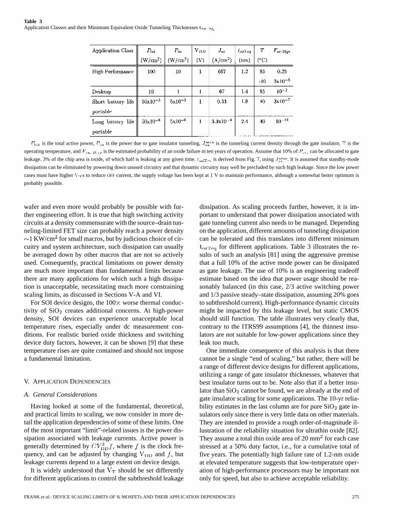
Table 3Application Classes and their Minimum Equivalent Oxide Tunneling Thicknessest
P is the total active power,P is the power due to gate insulator tunneling,J is the tunneling current density through the gate insulator,T is the
operating temperature, andF is the estimated probability of an oxide failure in ten years of operation. Assume that 10% ofP can be allocated to gate
leakage. 3% of the chip area is oxide, of which half is leaking at any given time.t is derived from Fig. 7, usingJ . It is assumed that standby-mode
dissipation can be eliminated by powering down unused circuitry and that dynamic circuitry may well be precluded by such high leakage. Since the low power
cases must have higherV s to reduceOFF current, the supply voltage has been kept at 1 V to maintain performance, although a somewhat better optimum is
probably possible.
wafer and even more would probably be possible with fur-ther engineering effort. It is true that high switching activitycircuits at a density commensurate with the source–drain tun-neling-limited FET size can probably reach a power density
1 KW/cm for small macros, but by judicious choice of cir-cuitry and system architecture, such dissipation can usuallybe averaged down by other macros that are not so activelyused. Consequently, practical limitations on power densityare much more important than fundamental limits becausethere are many applications for which such a high dissipa-tion is unacceptable, necessitating much more constrainingscaling limits, as discussed in Sections V-A and VI.
For SOI device designs, the 100worse thermal conduc-tivity of SiO creates additional concerns. At high-powerdensity, SOI devices can experience unacceptable localtemperature rises, especially under dc measurement con-ditions. For realistic buried oxide thickness and switchingdevice duty factors, however, it can be shown [9] that thesetemperature rises are quite contained and should not imposea fundamental limitation.
V. APPLICATION DEPENDENCIES
A. General Considerations
Having looked at some of the fundamental, theoretical,and practical limits to scaling, we now consider in more de-tail the application dependencies of some of these limits. Oneof the most important “limit”-related issues is the power dis-sipation associated with leakage currents. Active power isgenerally determined by , where is the clock fre-quency, and can be adjusted by changing and , butleakage currents depend to a large extent on device design.
It is widely understood that should be set differentlyfor different applications to control the subthreshold leakage
dissipation. As scaling proceeds further, however, it is im-portant to understand that power dissipation associated withgate tunneling current also needs to be managed. Dependingon the application, different amounts of tunneling dissipationcan be tolerated and this translates into different minimum
for different applications. Table 3 illustrates the re-sults of such an analysis [81] using the aggressive premisethat a full 10% of the active mode power can be dissipatedas gate leakage. The use of 10% is an engineering tradeoffestimate based on the idea that power usage should be rea-sonably balanced (in this case, 2/3 active switching powerand 1/3 passive steady–state dissipation, assuming 20% goesto subthreshold current). High-performance dynamic circuitsmight be impacted by this leakage level, but static CMOSshould still function. The table illustrates very clearly that,contrary to the ITRS99 assumptions [4], the thinnest insu-lators are not suitable for low-power applications since theyleak too much.
One immediate consequence of this analysis is that therecannot be a single “end of scaling,” but rather, there will bea range of different device designs for different applications,utilizing a range of gate insulator thicknesses, whatever thatbest insulator turns out to be. Note also that if a better insu-lator than SiO cannot be found, we are already at the end ofgate insulator scaling for some applications. The 10-yr relia-bility estimates in the last column are for pure SiOgate in-sulators only since there is very little data on other materials.They are intended to provide a rough order-of-magnitude il-lustration of the reliability situation for ultrathin oxide [82].They assume a total thin oxide area of 20 mmfor each casestressed at a 50% duty factor, i.e., for a cumulative total offive years. The potentially high failure rate of 1.2-nm oxideat elevated temperature suggests that low-temperature oper-ation of high-performance processors may be important notonly for speed, but also to achieve acceptable reliability.
FRANK et al.: DEVICE SCALING LIMITS OF Si MOSFETs AND THEIR APPLICATION DEPENDENCIES 275

The following sections explore in more detail scaling limitissues for some of the more important classes of applications.
B. DRAM
1) Scaling Challenges for DRAM:Although DRAMsand microprocessors share a common technology base,their product requirements and technical challenges areconsiderably different. DRAMs are driven by the goal of re-ducing cost/bit in each generation, which has been achievedby having greater density and more efficient productionof larger chips with larger starting Si substrates. DRAMsgenerally use higher internal voltage to store maximumcharge in the memory cells and there is a requirement for lowleakage to minimize the refresh activity. Microprocessorsare driven by the demand for higher and higher speed. Thehighest performance processors are now going to lowervoltage levels to keep the much higher chip power withinreason. Leakage current does not need to be as low as forDRAMs, except in some battery-powered applications.
Because of these requirements, the CMOS technologyused in microprocessors has been scaling to small dimen-sions at a faster pace than that used in DRAMs. As scalingof both DRAM and microprocessors continues into the 21stcentury, clearly there will be a drive to integrate them at thechip level to increase the memory bandwidth as demandedby the faster processors. This will place a premium onDRAM speed for some applications while density andcost will remain the driver for the large-volume memoryapplications.
The steady progress in DRAM up to the present has beendriven by dimensional scaling of the devices and wiringplus continuous improvements in the basic memory cell toachieve a more compact areal layout, such as the use oftrench or stacked capacitors. While there is some opportu-nity for further scaling of DRAM devices, it is becomingvery difficult to find still more compact cell arrangements.Here we discuss first the scaling of devices and voltagesin DRAM and then the challenges and possibilities forimproved cell concepts and structures.
2) DRAM Devices and Voltage Scaling:DRAM memorychips, for a given lithography capability, now use longerchannel lengths and higher voltage levels on the gate com-pared to the performance-oriented logic devices in order tostore more charge on the capacitor. Most present circuitsachieve a voltage difference on the capacitor which isabout 1.5–1.8 V less than the peak voltage applied to thegate of the memory cell devices. This is because of the needfor a high-threshold voltage in the memory cell devices( 0.8 V) to prevent subthreshold conduction of charge fromthe capacitor to the bit line at times when the bit line is at alow voltage and because of body effect, threshold tolerances,and signal required to turn on this device adequately towrite the high-level into the capacitor. In the future,as DRAMs are scaled to smaller dimensions, the voltagethat can be applied to the memory devices will follow apath similar to logic devices (but delayed in time) becausethose devices are at maximum field strength for gate-oxidereliability in any given generation [83]. Therefore, the stored
(a)
(b)
Fig. 25. Negative wordline voltage technique for DRAM memorycells. (a) Memory cell schematic. (b) Scaling path forV versusV .
voltage on the capacitor will shrink rapidly as the voltagesare scaled down unless a better technique is found. Also itis very difficult to achieve such a high in these scaleddevices, at least with the usual poly-Si gates.
A basically better arrangement, which has been used insome DRAMs, is shown in Fig. 25 [84]. It uses a lowerthreshold device that is easier to make and allows a highervoltage level to be stored on the capacitor for a givenwordline up level . Leakage of charge back through thedevice is shut off by keeping the turned-off gate negativecompared to the lowest source voltage on the bit line or onthe capacitor, which is zero in this case. When the transistoris turned on to write or zero into the capacitor, the gateis stressed to for the case of zero on the bit line. Thetable in Fig. 25 lists the estimated capacitor voltage that canbe stored as a function of the maximum device voltage .This assumes that the body effect, threshold tolerances, andsignal required on the device all scale down as the device isscaled to operate at the lower .
Up to now, DRAMs have commonly used a thinner equiv-alent for the storage capacitors in the memory cells com-pared to the used for the gate insulators. This has tendedto maximize the charge stored on the capacitors consideringthe lower voltage stress on them. Sustaining this trend withfurther scaling appears to be challenging. Rather than simplymaking the capacitor insulator thinner, which will soon leadto high tunneling current, this suggests that higher dielectricconstant materials will be needed. The leakage current re-quirement for the capacitor is quite stringent because of thelarge area involved. If SiOwere used, the limiting thick-ness would be about 3 nm for trench capacitor structures( 10 A/cm leakage). The commonly used nitride–oxidecomposite can be scaled to a somewhat thinner equivalentoxide thickness than that, perhaps 2.5 nm.
The leakage current requirement for DRAM is also a sig-nificant challenge for scaling of the cell transistor. AlthoughDRAM devices are properly turned off with the scheme of
276 PROCEEDINGS OF THE IEEE, VOL. 89, NO. 3, MARCH 2001

Fig.25 there is aconcern thatdrain junction leakageat the gateedge(alsoknownasgate-induceddrainleakage,orGIDL)maydischarge the capacitor [85]. This effect is greatly alleviatedwhen the junction voltage approaches the Si bandgap. How-ever, tunnelingcurrent in the drain-body junctiondue toheavybody doping is a concern for devices using a heavy “halo”or pocket implant. The tunneling current density that can beallowedinthejunctionisabout10 A/cm .Thisisreachedforabackgrounddopingdensityofabout310 /cm foranidealjunction [26], but may require a much lower concentrationbecauseofdefects [34].
Tunneling current through the gate insulator is also a con-cern. With the gate of the array transistor biased to a nega-tive value, relatively few electrons can tunnel from the gateinto the weakly inverted channel and only a portion of thesewill flow to the drain. The potentials are favorable to tun-neling in the gate–drain overlap region, but the gate–draininsulator thickness can be increased relative to thein thechannel region by a “bird’s beak” created in the gate-reox-idation process. It appears, therefore, that the most criticalregion is the boundary between the “bird’s beak” and thechannel, where the oxide is thinner but the channel potentialis still near that of the drain. In this region a current densityof A/cm can be tolerated, which corresponds to aaround 2.5 nm for the biases of interest.
3) Future Directions: From the above considerationsit appears that DRAMs can be scaled to effective channellengths of 50–100 nm if a direction for increasing the capac-itance/unit area is found. However, it will be very difficultto continue the past trends in compacting the memory cell,i.e., decreasing the size normalized in lithographic squares.The present approach, which gives about eight squaresper cell, can only be improved significantly by going to avertical structure for the device as well as the capacitor.Such structures have been proposed for some time, but noideal solution has been found. The approach of Grueninget al. [86] looks interesting and appears to be capable ofreducing the cell area to six squares.
Undoubtedly, progress in scaling DRAM will continuefor some time to the degree that lithography advances andthe increased density on a chip will allow new systems ap-proaches. It seems likely that today’s conventional DRAMwill be embedded with microprocessors on the same chipsand speeded up by utilizing the microprocessor devices andarchitectural improvements [87], while chips that performonly the memory function will continue to emphasize den-sity, slower speed, and perhaps nonvolatility. Thus, DRAMmay evolve in more than one direction in the future.
C. SRAM Limits
For most large logic applications, the SRAM is a highlycritical component. The SRAM cache access time is a criticalpart of the system access time. A large fraction of the tran-sistors in a modern processor chip are in SRAMs, impactingthe density and standby power of the entire chip. There areseveral different types of SRAM in use in these systems, soit is important to understand their different requirements.
Fig. 26. Six transistor Static RAM cell. Cell is addressed by thewordline (WL) and the data is read out via the bit line pair (BL).Inset shows a set of superimposed transfer curves for the two halvesof the SRAM cell showing how the noise immunity (shaded box) isaffected by a threshold voltage shift in one of the halves.
A typical high-speed SRAM uses the standard six-devicecell configuration as shown in Fig. 26. The typical area ofthese high-performance SRAM cells ranges from about 100to 200 lithographic squares. This is to be compared withonly eight squares for a DRAM cell and even smaller areasfor some nonvolatile memory cells. Why, then, does the in-dustry tolerate such an inefficient use of silicon area? Themain factors determining this are high speed, compatibilitywith logic, and the use of caching. These factors mean thatperformance has much more weight than density, at least inthe first level (L1) cache designs since demands for higherdensity can be shunted up the memory hierarchy. To ap-preciate the memory hierarchy in the context of technologyevolution, consider Fig. 27. This figure shows how a largerpart of the memory hierarchy is placed on-chip as the tech-nology progresses. Stand-alone SRAM, which today has im-portant uses both for cache and in signal processing sys-tems, will probably become part of a larger on-chip system inthe future. For instance, a recent microprocessor unit (MPU)[88] features 32-kB instruction and data caches as well as anon-chip 256-kB L2 cache. In the future the L1 cache is likelyto increase fairly slowly in size to maintain its high speed,whereas several megabytes of L2 cache might eventually beused and perhaps even additional levels of hierarchy wouldbe incorporated on chip.
Practically, this means that the speed-critical SRAM,which must use the general logic technology, becomes asmaller part of the total chip and issues of power dissipationbecome less important for this part. These SRAMs becomemerely an extension of the logic technology with no specialconsideration as to density, standby power, etc. Fairly largesubthreshold currents can be tolerated; for instance, a 64-kBcache ( current paths) at a power supply voltage of 1
FRANK et al.: DEVICE SCALING LIMITS OF Si MOSFETs AND THEIR APPLICATION DEPENDENCIES 277

Fig. 27. Evolution of the memory hierarchy with increasingintegration level (a) CPU and Cache on separate chips. (b) CPU andCache on the same chip. (c) CPU+ 2 level cache on one chip.
V can tolerate A/ m of leakage current for 1-W powerdissipation, which is consistent with low FETs.
The picture is very different for the L2 cache, whichnow has a relaxed speed (latency) requirement comparedto the L1 cache, but is much larger. Many tradeoffs canbe made for speed versus density and completely differenttechnologies can, in principle, be incorporated such asDRAM, floating gate and thyristor memories [89], whichuse silicon technology but add processing steps to theCMOS logic process, or memories such as ferroelectricand magnetic RAM, which introduce new materials, withthe cost being the determining factor. Given the designlatitude with emphasis on density rather than speed, otherSRAM approaches than the 6-T cell such as 4-T and 5-Tversions or cells using resistor loads placed above the cells(or preferably thin-film transistor loads) to reduce standbypower might find their place. At the cost of the addedtechnology involved in stacked load devices, SRAM cellsize can be reduced to the 50–100 square range, but thisis currently practiced only for stand-alone SRAM chips.The 4-T cell has reduced static noise margin (on read) ascompared to the 6-T cell, especially at low voltages [90], butthere will still be a great incentive to use these designs giventhe increased density, where the noise margin issue can becountered with appropriate choice of voltage (see below)and a less demanding speed requirement.
A conventional SRAM L2 cache would still be thecheapest choice for many applications since it does not addany processing cost if it uses the general logic technologyalthough even here, modest technology enhancements toimprove density, such as buried contacts, may prove tobe cost effective. Cell layouts may be used that maximize
density rather than speed by using narrower transistors andusing the multilevel wiring capability for the crossovers.Further density improvement can also be obtained by repar-titioning the SRAM to reduce peripheral circuitry. The L2SRAM would need high-threshold voltage transistors in thecells to minimize device leakage as well as a thicker gateoxide to reduce gate leakage. Such options are already beingincorporated into today’s technology and will continueto be necessary in future scaled logic technology. The L2cache would most likely also use longer channel lengthFETs to reduce rolloff variations. The longer channellength would not impact the cell size severely because allof the other groundrules will remain unchanged. The higherthreshold cells will also need a higher power supply voltagethan the general logic and a higher swing from the wordlinedrivers to adequately turn the transfer devices both on andoff [91]. To save dynamic power, the bit lines and senseamplifiers may run at the somewhat lower voltages of thegeneral logic [92]. Dual or multiple power supplies willprobably be available from the future technology for theseand other purposes.
The above scenario, which is very likely, leads to the pos-sibility that most of the standby current leakage requirementsof the chip could be shunted to a less demanding technologyin terms of threshold voltage, channel length, gate leakage,and reliability, leaving more freedom for the logic technologyto be optimized for performance.
Potential issues for future SRAMs are soft errors due toscaled-down voltage and capacitance and hard fails due tothreshold voltage variability of the small in-cell FETs due torandom dopant fluctuations and other processing issues. Bur-nettet al.[78] investigated cell stability under random dopantfluctuations and showed how this leads to increased voltagerequirements for the cell in scaled technologies. In practice,redundancy techniques can and are being used to reduce theimpact of the hard fails [88] and error-correction techniquescan reduce the soft error rate to an acceptable level. Alter-nate technology choices such as thin SOI with or without adouble gate could reduce soft errors through decreased col-lection volume and hard errors by eliminating (or reducing)the body doping.
D. Low-Power Applications
There is a steadily growing market for low-power appli-cations of CMOS technology and it is the battery-powerednature of most of these applications that particularly createsthe low-power constraint. To achieve good battery life, thesecircuits simply cannot dissipate very much power. Roughlyspeaking, these are circuits that consume less than 1 W/cmwith a subgroup of ultralow power circuits in the range below1 mW/cm . Higher power applications are discussed in thenext section.
Low-power constraints fall into two broad categories:those that relate to active mode power dissipation andthose that relate to dissipation in the quiescent state. Sometypes of applications are primarily sensitive to active powerconsiderations, since they are switched off when not in
278 PROCEEDINGS OF THE IEEE, VOL. 89, NO. 3, MARCH 2001

use. Other applications may be turned on almost all thetime, but rarely ever actually compute anything and so aremore concerned with the quiescent power dissipation. SinceMOSFET design limits are different for these two cases,they need to be considered separately.
Reducing active power begins at the top. The most effec-tive place to reduce power dissipation is almost always atthe highest level of the problem definition. Redefining theproblem, the architecture, the algorithms, and/or the proto-cols can often save several orders of magnitude in power dis-sipation. The development by Menget al. [93] of a portablevideo-on-demand chip set using only 10 mW is an exampleof this.
At the device design level, the important low-power vari-ables are the threshold voltage, the gate leakage current, andthe device size, which largely determines the body-to-draintunneling dissipation. For current generations of technology,the latter effect is not usually significant, but at the limits ofscaling, it should become quite important. For active modedissipation, these parameters offer strong tradeoffs betweenspeed (at low , thin oxide, and small devices) and lowpower (at higher , thicker oxide, and larger devices). Thistradeoff occurs because all three variables tend to simultane-ously increase the circuit’s speed and its dissipation duringthe time it is not switching.
The optimization of the and tradeoffs for lowpower has been well studied [44]–[46], including the effectsof process and supply variations, which are quite important.The study by Franket al. [46], for example, shows thateven in the presence of realistic variations, the optimumsupply voltages can readily drop below 1 V and can reach0.5 V under some conditions (high switching activity andswitching speed target 5–10slower than the maximumtechnology capability). The optimum value for increasesfor slow circuits to reduce static dissipation and increasesby 20–100 mV when the tolerances are doubled from theirnominal (realistic) values. The dependence of the optimumdesign points on activity factor and logic depth is illustratedin Fig. 28. These particular optimizations are for 0.1-mstatic CMOS arithmetic circuits and each point in the figurerepresents an independent optimization of both the supplyvoltage and the threshold voltage. Optimization of the gatelength at the 0.1-m generation was a weak effect, but atthe limits of scaling it will be very important because ofbody-to-drain tunneling, as discussed in Section VI. Asshown, the optimum nominal threshold voltage dependsstrongly on activity factor and logic depth, so that in thelimit of minimum power, a wide range of s are needed tosatisfy the requirements of a range of applications.
The optimization of oxide thickness for low-power con-sumption has only recently become a concern and so has notreceived significant study. The rough estimate used in Sec-tion V-A of 10% of the total power allocated to gate leakageseems reasonable as a first pass. Based on this estimate, asindicated in Table 3, the likely minimum varies from
2.6 nm for ultralow-power applications to1.7 nm formoderate low power, although it could go somewhat thinner
Fig. 28. Plot of supply voltage and threshold voltage versusthe activity factor-to-logic depth ratio for four different delayconstraints. Logic depth= 4n = 48, 40, 28, and 8 for thedata points from left to right across the plots. Threshold voltagehere is the gate voltage at whichI linearly extrapolates to zero.Data is from [46].
for cases in which the optimum supply voltage is well belowthe 1 V used in the table.
Quiescent power constraints are often much lower thanthe optimized background dc dissipation during active mode.This means that the optimum active mode FET design cannotsatisfy the quiescent constraints. This problem can be ad-dressed in at least three different ways: 1) one can use higher
FETs throughout the design, so that the quiescent powerrequirements will be met; 2) one can dynamically change thebody voltage (or backgate voltage for double-gated struc-tures) to switch between a high- quiescent state and alower active state; and 3) one can put series switches inthe power supply to turn off inactive circuit blocks.
The drawback to using higher FETs throughout isthat one must then raise the supply voltage to maintainadequate performance in the active mode. One must also usethick enough oxide that its quiescent leakage satisfies theconstraint, requiring still higher to retain performance.The device size must also increase to support the increasedvoltage without increasing the body-to-drain tunnelingcurrents. Thus, the active mode is likely to consume muchmore than the minimum required power, making this aninefficient option unless extremely little active power is everrequired.
Dynamically adjusting using the body voltage is an in-teresting option which has also been suggested as a way ofcompensating out process-induced threshold variations. Thebiggest disadvantage of this approach is that it only elimi-nates dissipation due to subthreshold leakage, but does nottake away the gate and body-to-drain leakage dissipation.There is also the question of whether body junction leakageand bias generation power may not exceed the subthresholddissipation one is trying to suppress.
The third option appears to be the best for logic circuits,since it eliminates all three forms of leakage dissipation,leaving in their place only the leakage dissipation asso-ciated with the series switch. The disadvantage here is in
FRANK et al.: DEVICE SCALING LIMITS OF Si MOSFETs AND THEIR APPLICATION DEPENDENCIES 279

controlling and powering the series switch, but this appearsfeasible. Another consideration is that it is not permissibleto power down the latches and SRAM if they are holdingdata that must be retained. Data-holding circuits seem tohave little choice but to use high-threshold voltages in orderto suppress quiescent dissipation. This line of reasoningstrongly suggests that low-power chips will require at leasttwo threshold voltages, one low and optimized for logic, andone high and optimized for holding data. It should, however,be possible to reduce the applied to data-holdingcircuits during quiescent mode, which would reduce theirtunneling currents.
E. High-Performance Applications
The last dozen years have seen tremendous growth ina specialized, but significant, application of CMOS logic,namely that of high-performance CMOS. This applicationis defined by products in which raw switching speed isthe primary goal of the process technology. Active powerdissipation is also a consideration, albeit usually a secondaryone. The role played by subthreshold leakage dividesthis application space into a few subcategories which wediscuss explicitly. Furthermore, as scaling continues intothe sub-100-nm regime, we expect that gate oxide leakageswill also place limits that differ by application in a similarmanner. The high-performance CMOS scaling trends since1990 were shown in Fig. 2 from which it is clear that assilicon manufacturers near production of the 0.13-m nodeof the ITRS roadmap [4], the industry is on the verge of aregime where there is no room to continue the past trendsfor threshold voltages.
1) Worst Case Limitations: As discussed at the be-ginning of Section IV, there are many sources of parametervariations in MOSFETs. For high-performance circuits, it isespecially important to understand the effects of varia-tions, in particular. These variations may be either intradieor interdie and are caused by process variations, gate-lengthvariations, process-induced proximity effects of neighboringstructures, stochastic doping effects, and other intradie fluc-tuations [94]. These variations enter into consideration inthree ways: 1) die-to-die and wafer-to-wafer variations in
, the average of a given chip; 2) an on-chip shiftin , the total quiescent current of a die; and 3) ,the worst case threshold voltage for any individual FET on adie.
The die-to-die variations in mean can be character-ized by an average value and a variance, althoughusually the worst case low average threshold is ofgreatest interest since it is usually the fastest performing,both because of the low and because low is gener-ally associated with shorter gates. Manufacturers sometimestake advantage of this spread by sorting the chips and sellingthe fastest ones at a higher price.
The intradie variations in at the individual FET levelare characterized by a Gaussian distribution with stan-
dard deviation . Using this distribution, one can calculatequiescent current
where is the number of FETs and is the qui-escent current that would flow if all the FETs on the entirechip had exactly the same threshold . Thus, it canbe seen that is raised by the factor dueto the variations in .
In addition to its obvious use in determining whethera chip satisfies the leakage requirements of its particularapplication, also plays an important role in reliabilitystrategies. Since is sensitive to several types of de-fects, including some that may not prevent functionality, itis used as a reliability criterion in many lower cost products.A measured low value indicates an absence of shorts anddecreases the likelihood of latent defects in shipped productsthat may fail later in the field. In less cost-sensitive arenasmany products are “burned in” by operating the product fora limited time at elevated voltages and/or temperatures. Bothsubthreshold conduction and oxide leakage are enhancedduring such burn-in conditions, resulting in very highquiescent current.
Finally, the worst case threshold voltage forany individual MOSFET, is limited as well in at least twoways. First, digital CMOS circuits require adequate noiseimmunity to function properly. This constraint should scaleat least approximately with and as a worst case, ithas been estimated that must be at least 10% of
based on analysis of 2.5- and 3.3-V logic technology[83]. Nominal design targets are usually around 25% of
. Second, some classes of high-performance circuits,such as dynamic logic, obtain performance advantage fromnFET-dominated switching (nFET evaluate trees) and usevery narrow pFETs or just node capacitance to hold theoutput high for a clock cycle prior to evaluation of thelogic. If the of a single nFET in such a position were tobecome too low, then subthreshold leakage would make thecircuit nonfunctional. Since there are a very large numberof devices on a chip, the statistics suggest that one shoulddesign to at least tolerances unless it can be shown thatthe distribution falls off faster than Gaussian for low
s.2) High Power (30–100-W/cm Active Power): For
high-power applications, is large, possibly reachingas high as 1 KW/cm in high-activity factor macros atend-of-scaling logic density. As a result, under normaloperating conditions the subthreshold leakage and gatetunneling leakage may be more limited by functionalityconcerns than by leakage power constraints. Becauseswitching power is dominant, these designs do drivetoward lower values which, in turn, drives down. On the
280 PROCEEDINGS OF THE IEEE, VOL. 89, NO. 3, MARCH 2001

other hand, the use of dynamic logic places an upper boundon individual FET leakage, creating a floor on valuesand forcing the use of somewhat larger thresholds thanwould be allowed by power considerations alone. Use ofmultiple threshold values [95] can moderate this constraint,but does not entirely remove the problem. A high degree ofreliability is usually required by systems employing suchtechnologies and often demands special screening and/orburn-in procedures. Voltages from 25% to 100% abovethe nominal operating supply voltage and temperatures ashigh as 160 C have often been employed. If, as is oftenthe case, circuit functionality is required at these elevatedtemperatures and voltages, then the floor necessary fordynamic logic and/or noise margins is raised significantly,especially compared to the low s suitable for chilledoperation. Furthermore, in the limit the device cannotbe scaled as far if it must sustain these higher voltages.Currently, the situation is accommodated by using ahigher than desirable at operation conditions, solely sothat burn-in conditions can be met. In future generationsof technology, this burn-in constraint could be met throughuse of body-bias (or back-gate control in DG-FETs) todynamically increase the during burn-in. In this case,it may be possible to push the nominal operating conditionleakage currents up closer to the logic functionality limit,enabling lower threshold and supply voltages. In the end,reliability testing will force high-reliability parts to be largerand slower than “unreliable” parts that do not require suchscreening, and if control is not used, they will be evenslower due to the need for higher s.
The past scaling trend in this arena has been to scalewith to maintain performance, while only
allowing logarithmic scaling of to contain increasesin the worst case leakage currents. Clearly this results in asteadily decreasing tolerance budget, which is gettingmore and more difficult to satisfy.
3) Medium-High Power (5–30 W/cm): This includeshigh-end desktop and midrange workstation processors. Forthese applications, leakage current can be limited by bothpower and functionality concerns, depending on design.Typically, leakage dissipation must be limited to somereasonable fraction of the total power budget at normaloperation conditions and at this level, it will not impactfunctionality. Already some recent technologies with leak-ages in the realm of 10 nA/m are beginning to experiencethis power limit. Reliability assurance will continue to be aburden, however, as in the high-power sector. These appli-cations may also have low enough s that functionality isimpacted during burn-in, possibly necessitating dynamicallyadjustable thresholds here, too. While the reliability require-ments are typically less demanding, costs associated withthe ability to burn in high designs may be prohibitiveand, thus, drive lower leakage constraints on andthan the high-power sector. If dual strategies are used,the low may be limited to 180 mV at 25 C based onthe use of for reliability measurements. Similarly,may be constrained to 1.2-1.5 nm of silicon dioxide with
a dual approach also likely to appear in order to bettermanage leakages.
4) Moderate Power (0.5–5 W/cm): Mobile processors,high-speed SRAM, and high-performance application-spe-cific integrated circuits (ASICs) fall within this category.
is limited simply due to power restrictions of the ap-plication. Loss of functionality due to leakage currents is notgenerally a concern. The low-power end of this range alreadyhas limited to 300 mV for 0.1- m MOSFETs andthese thresholds will have to increase as scaling continues.Since quiescent power requirements are often much lowerthan the optimum active mode leakage power, gate oxidesmay be limited to a thicker range (1.7–2.0 nm) than wouldbe possible for active mode optimization alone (1.3–1.6nm). This application area is already experiencing smallerreturns in performance with scaling than obtained inthe past as a result of these pressures. Various well-biasingand power-supply switching schemes have been proposedas a means of allowing lower for further performanceleverage, but it is presently not clear just how much relief ispractical. Techniques that either modify dynamically orpower locally must also be able to respond with verylittle delay. As a result, many solutions for the low-powerarena (see Section V-D) may not be practical here.
VI. DISCUSSION
Having described in some detail many of the physical ef-fects that limit scaling of CMOS and the specific details ofthese limits for various applications, we now attempt to dis-till all of this information into a single table, Table 4. Thistable is intended to show the general landscape more thanexact values and is compiled in the same spirit as Table 3:power density is the overriding parameter and the leakagemechanisms are each allocated as a certain fraction of thetotal power. More detailed optimizations might well changethese fractions somewhat, but the overall trends described inthe table should still be valid.
Table 4 is oriented around the power dissipation for activecircuits. This focus is based on the assumption that quies-cent power dissipation requirements during periods of longinactivity are best met by switching off the power supply.For applications for which this is not possible, it will be nec-essary to use higher thresholds, thicker oxides, and less ag-gressive doping than their active power limits would permit.As is the current practice, it is expected that multiple tech-nologies may be present on the same chip, each optimizedfor its own particular power density target. Nevertheless, theassumption that the active power can be arbitrarily set towhatever limit the application demands needs further exam-ination. The high-performance logic proposed in this tableshould easily be able to dissipate dynamic power at a rate of1000 W/cm if run at full speed with a fairly high activityfactor (as is common for much of the logic in a high-perfor-mance processor). This is already ten times higher than one isprobably willing to dissipate at the package. By lowering thespeed somewhat, moving toward narrower longer devices at
FRANK et al.: DEVICE SCALING LIMITS OF Si MOSFETs AND THEIR APPLICATION DEPENDENCIES 281

Table 4Estimated Scaling Limits for Various MOSFET Design Parameters and their Dependence onApplication Class and Device Type
I ,V andt are worst case values. Low temperature (�170C) bulk cases assume a forward body bias of 0.5 V, while all of the other bulk cases
assume no forward body bias. PFETjV j is expected to be�50 mV lower thanV . To facilitate comparisons between cases, more precision is shown
in some cases than is warranted on an absolute scale. Parameter ranges are intended to span the range of requirements and limits that might exist withinthe
different application classes and are all organized in the same sense (from most aggressive scaling to least) with power andV being independent variables.
indicatesI is limited by functionality concerns rather than by leakage dissipation.indicatesL is limited by source-to-drain tunneling rather than
by scale length. indicatesV is limited by noise margin requirements (10% ofV ) rather than byOFF current.
the lower power end of the table, and optimizing the thresh-olds and supplies for “low power,” one may be able to lowerthe dynamic energy consumption per switching event by per-haps an order of magnitude. The speed of these technolo-gies probably also decreases about an order of magnitudefrom the high-performance V cases tothe V longer channel low-power cases.So, the overall situation is that the energy per logic opera-tion only varies by about one order of magnitude over thistable and the speed varies another order of magnitude, whilethe desired power varies by over six orders of magnitude. Sohow will the power density be lowered to the levels specifiedin the table? There are several approaches: 1) chips hardlyever use all of their circuitry so actively (by averaging overthe less active areas and over large areas of lower dissipa-tion SRAM or DRAM, one can probably reduce the powerdensity an order of magnitude); 2) one can lower the clockfrequency until one’s throughput requirements are only justsatisfied (this may also enable a further reduction in ,although cannot get too close to because thresholdvariations cause too much timing uncertainty); 3) one can run
the chip in bursts of power-optimized activity and turn it offbetween bursts; and 4) one can design the chip as many spe-cial purpose macros, each power- or energy-optimized for itsspecific task. The chip would then shuffle its work among themacros, minimizing the energy consumed, and increasing theaveraging used in 1).
The methodology that has gone into creating Table 4 is asfollows. Under worst case conditions (shortest gate length,lowest , thinnest insulator, highest temperature) 20% ofthe total power is allocated to subthreshold leakage currents,10% is allocated to oxide tunneling currents, and 5% is al-located to band-to-band tunneling through the body-to-drainjunction. These somewhat arbitrary percentages are chosenwith the overall intent of allocating 2/3 of the power touseful switching, as in Section V-A. Since the final scalinglimits are only logarithmically dependent on these percent-ages, the exact values are not critical. If
, we assume there is no body-to-drain tunneling be-cause the bands do not line up. For definiteness, we havetaken mV. The supply voltages do notrepresent scaling minima, but rather are simply estimates of
282 PROCEEDINGS OF THE IEEE, VOL. 89, NO. 3, MARCH 2001

what we think will constitute reasonable supply levels forobtaining good performance. The supply voltage rises forultralow-power applications simply to maintain some per-formance in the face of rising threshold voltages. The sub-threshold slope is obtained from the given temperature andan assumed ideality factor at shortest gate length of 1.4 forthe nonbody-biased bulk cases, 1.6 for the forward-body-bi-ased bulk cases (those at170 C), and 1.2 for the DG-FETs.The preceding are the only places where temperature enters:the tunneling processes are assumed to be temperature-inde-pendent.
The remaining variables are calculated self consistentlyusing a spreadsheet. Beginning at the end, the nominalchannel length is used to derive a total device widthper cm of Si, assuming that gates occupy 3% (estimatedfrom ITRS99 [4]) of the total Si area and that the physicalgate length is 40% longer than the effective channel length
. Assuming that on average half of the FETs are intheOFFstate and contributing leakage current, the allocatedsubthreshold power is divided by the supply voltage and
to obtain . TheOFF current is, however, limitedto a maximum of 1000 nA/m as a rough estimate of thecircuit functionality constraint. If the functionality constraintis reached, the gate and body-to-drain tunneling currentsare also limited to 500 and 250 nA/m, respectively.The nFET threshold voltage is then obtained from
, where is 300 nA for bulkdevices and 600 nA for DG-FETs (since they effectivelyhave twice the width). The maximum gate insulator tun-neling current density is determined by dividing the powerallocated to gate tunneling by the supply voltage and halfthe total gate area, again on the assumption that only halfthe gates are in the turned-on state. DG-FETs use 6% forthe total gate area since there are two surfaces, which areassumed symmetric for this analysis. This tunneling currentdensity is translated into a minimum equivalent tunnelingoxide thickness using the curves in Fig. 7. We areoptimistically assuming here that oxide/insulator reliabilityproblems can be solved to the extent that they will notimpose lower current density limits for the supply voltagesconsidered. If these problems cannot be solved, the high-per-formance cases might need substantially thicker insulators,possibly increasing their channel lengths 10%–20%.
The minimum scale length is derived from thebody-to-drain tunneling constraint. For the 25-nm bulkdesign the vertical extent of the body-to-drain tunnelingregion is 10–15 nm, which is (see Fig. 15). Wehave assumed that this dimension will scale with channellength (and that half the FETs are in theOFFstate) and so thepower allocated to this tunneling is divided by the supplyvoltage and times to obtain a maximumtunneling current density, which is converted into a max-imum field using the curve in Fig. 9. is thenobtained from this field by scaling the 25-nm design point:
MV/cmV), where nm, and isthe drain-to-body voltage. The calculation for DG-FETs issimilar except the cross-sectional area for tunneling uses the
Si film thickness instead of half the channel length. In thiscase, is determined by scaling from a nmDG-FET simulation as a function of .
Next, is evaluated using the preceding ,and the scale length theory presented in Section II-A and theAppendix. Since these are supposed to be limits to scaling,we assumed that the gate insulator is like AlO with atunneling barrier similar to SiO, but twice the dielectricconstant. If alternate dielectric materials cannot be usedand FETs are stuck with oxy-nitrites, then the channellengths in Table 4 would need to be increased 0%–20%depending on the extent to which the increased insulatorthickness can be countered by thinning . For DG-FETs,if the computed is smaller than the minimum Si layerthickness (5 nm, based on the tolerance-related principlesdiscussed in Section IV-B) or if it does not exist because
, then is set to 5 nm andis recomputed from and . For the cases in whichsource-to-drain tunneling constrains the value of , weset to yield the constrained value for since thereis no point in making it smaller.
Finally, the nominal channel lengths are determinedby multiplying the scale length by 1.5 for logic MOSFETsand 1.6 for the DRAM. This assumes that both bulk andDG-FETs have some sort of compensation for rolloff(e.g., halos), although the feasibility of such compensationfor the smallest devices is certainly questionable.
This table reveals the dependence of scaling limits onapplications very clearly. As one moves from high- tolow-power applications, the shrinking leakage requirementscause the minimum allowed nominal channel length for bulkMOSFETs to increase from 14 nm to 38 nm, almost3 , while increases from 1 to 2.6 nm. DG-FETschannel lengths also increase from 13 to 33 nm, revealing a10%–50% scaling advantage depending on conditions. Theadvantage is low for the shortest channel cases because bothdevices are limited by source-to-drain tunneling and is alsolow for the high , high cases where the DG-FET ismore impacted by body-to-drain tunneling. For the majorityof applications, however, especially those at lower ,the DG-FET shows a very substantial advantage, equivalentto an entire generation of scaling. The dependence isparticularly evident in the ultralow-power case. Note thatthe DG-FETs tend to have lower threshold voltages forthe low-power cases because of their steeper subthresholdslopes, but this is partly compensated by decreasingre-quirements due to their greater density. On the performanceside, the DG-FETs can probably significantly outperformtheir bulk counterparts in wiring capacitance-dominated cir-cuits because of their effectively doubled current drive (twogated surfaces). Overall, for both device types, traditional
ratios only appear to be achievable for the highestperformance design point. The lower power points requireprogressively higher ratios than have been used historically.
The temperature dependence of the high-performancedesign points shows that although temperature may notbuy any advantage as far as minimum channel length isconcerned, it should allow lower voltage operation. This is
FRANK et al.: DEVICE SCALING LIMITS OF Si MOSFETs AND THEIR APPLICATION DEPENDENCIES 283

very important since lower voltage means lower energy perlogic operation and, hence, more operations can be doneper second for the same total chip power dissipation; i.e.,the clock can be sped up or the logic made more dense.The low temperatures should also enhance device speed byimproving mobility. The 170 C 0.5-V design points areinteresting because their nominal design points are limitedby source-to-drain tunneling rather than by their scalelengths. This is because source-to-drain tunneling interfereswith the steep low-temperature subthreshold slopes a littlesooner than it strikes the less-steep room temperature curves(see Section III). The high-temperature burn-in limited caseshows that the scale length must be increased significantly tosatisfy the high burn-in voltage requirement. Also, mustbe set quite high to meet margin requirements well above thedesired for the lower temperature operating conditions,resulting in further reduced performance if a dynamicallyadjustable approach (e.g., body-biasing) is not adopted.
The DRAM design points are based on the criteria inSection V-B and show two possibilities with regard toachieving the necessaryOFF current. For the wordline (WL)not going below ground, a midgap workfunction metalgate would probably be necessary to achieve the desiredthreshold. For a negative wordline-low voltage, however,a more reasonable logic-like threshold could be used, asdescribed in Section V-B.
The bulk MOSFET projections in Table 4 all assumethat the body is at a fixed bias of zero, except for the
170 C cases, which assume 0.5-V forward bias. ForPD-SOI MOSFETs, this is not usually the case. The highdrain-to-body tunneling currents assumed in these extremelyscaled FETs would forward bias the floating body muchfurther than occurs in current designs. From the point ofview of scale length, this would seem advantageous becauselike the 170 C case, it would reduce the depletion depth,which would enable further scaling. Another effect is thatthe forward body bias may be strongly dependent on thedrain voltage, potentially causing large output conductancesuch as that seen recently in 52-nm physical gate lengthPD-SOI [96]. If is increased on the DG-FET designs,the same sort of effect would be expected. More research isneeded into this regime to determine the relative advantagesand disadvantages of forward body bias and high outputconductance in SOI.
These scaling limit projections rest mostly on the leakagecurrent mechanisms discussed earlier in this paper. Howaccurate are they? The required threshold voltages shouldbe reasonably accurate since they depend only on the
definition itself and the well-understood dependenceof the subthreshold current on and ideality. Only forthe high-performance DG-FET and170 C cases doesthe subthreshold enter into the less-well characterizedsource-to-drain tunneling regime. The requirementsare based on oxide tunneling curves that have been wellmeasured in recent years. Although there is some disagree-ment about how to determine the physical thickness of verythin oxide layers, should really be thought of as aparameterization of the current density that can be applied to
any insulator. Unfortunately, the most sensitive parameter indetermining the minimum scaling dimension is the depletiondepth, which is determined from the band-to-band tunnelingcurve in Fig. 9. This curve admittedly rests on relativelylittle data and deserves much further investigation becauseit plays such a prominent role in the end of scaling.
For the DG-FET limits, one big uncertainty about theseprojections is the question of whether high channel mobilitycan indeed be obtained since this has not yet been success-fully demonstrated experimentally. Also, obtaining the de-sired s is difficult for DG-FETs since the channel is notthick enough to allow shifts of more than about100 mVby use of doping without causing excessive fluctuationsdue to the discreteness of the dopants [54]. Indeed, it wouldbe better not to put any dopants in the channel at all. Conse-quently, the DG-FET design points probably require the de-velopment of several different metal gate technologies withsuitable workfunctions. Drain-to-floating-body tunneling inDG-FETs is also an issue and needs further work.
Although the designs presented in the table account for25% lithographic variation in channel length by setting the
nominal channel longer than the minimum channel length,they do not explicitly take into account threshold variationsdue to dopant fluctuations. As pointed out in Section IV-C,these variations are already substantial for the 25-nmMOSFET design and will only grow larger in scaling to the15-nm design point suggested in the table. This problemprimarily afflicts the bulk designs (if the DG-FET s areobtained by workfunction adjustment) and will necessitateraising the targets—especially for SRAM. This effectappears to give an added advantage to DG-FETs.
For lack of expertise, we have not discussed analog deviceapplication constraints in this paper, but a few general com-ments are possible. Two of the main requirements of analogapplications are “higher” supply voltages (1.5–2.0 V oftenseems to be the minimum acceptable) and high-output re-sistance. The higher voltage will necessitate thicker oxide,2–3 nm depending perhaps more on reliability concerns thanon leakage current. The high-output resistance translates intoa large ratio according to Fig. 5, perhaps 3.0 or more.Based on these assumptions, it appears that the scaling limitfor generic analog applications is considerably larger than forlogic, probably in the 80-nm channel length regime.
VII. CONCLUSION
We have described most of the important physicalphenomena that stand in the way of continued scaling ofSi CMOS technology and have shown how these effectsdetermine different limits for different circuit applications.Most of the application limits are set by limitations on theamount of power that can be dissipated in the three primaryleakages: subthreshold channel current, gate-to-channeltunneling through the insulator, and body-to-drain junctiontunneling currents. Source-to-drain tunneling along thechannel is also a possible limitation for very short channelsand at low temperature.
284 PROCEEDINGS OF THE IEEE, VOL. 89, NO. 3, MARCH 2001

The scale length theory that has been presented here pro-vides a useful framework within which to understand thetradeoff between channel length and short channel effects.Using this theory in conjunction with the various limitingeffects, we have projected that bulk-like CMOS should beextendible down to about 14-nm nominal channel length forhigh-performance logic and35 nm for very low power ap-plications, with intermediate applications falling in between.DG-FETs are projected to be scalable to 10%–50% shorterchannel lengths than their bulk counterparts with the greatestadvantage being at low-supply voltages. These estimates in-clude allowance for reasonable tolerances between nominaland worst case channel lengths as required for current manu-facturing processes, but for experiments in which tolerancescan be ignored we have discussed several results for FETswith channel length in the 8–12-nm range.
Overall, we conclude that there is no single endpoint toscaling of CMOS. Rather, there are many endpoints, each op-timally adapted to its particular applications. As the industrymoves forward, greater flexibility will have to be developedin manufacturing different devices for different users.
APPENDIX
Following the method of [19], consider the idealizedMOSFET cross section in Fig. 3(a), which defines, , thedepletion depth , and the dielectric thickness . Usingsuperposition, the potentials and in the center of theFET can be written as
(A1)
where the satisfy Poisson’s equation for the fixedcharges (usually nonuniform) in the device with allboundary potentials at zero, are the one-dimensionalsolutions to Poisson’s equation satisfying the gate voltage,body voltage, and dielectric boundary conditions, andand are left and right solutions to Laplace’sequation, which accommodate potentials applied to thesource and drain [21].
These s can be written as infinite series, but the lowestorder term is the most important, since the higher terms decayvery rapidly
(A2)
where the s, s, and are coefficients to be deter-mined by satisfying the boundary conditions. These formsare chosen to provide at the andboundaries and one half period of the sine functions in be-tween. As shown in Fig. 4, these analytic solutions very accu-
rately approximate the potential variation along the channelunder the gate.
By constraining the upper and lower analytic solutions tosatisfy the usual dielectric boundary conditions at , onecan arrive at an equation for the eigenvalues, of whichisthe smallest
(A3)
or, in terms of the scale length
(A4)
In a similar manner, a device containing three layers ofdielectrics with thicknesses, , and and dielectric con-stants , , and can be solved for an eigenvalue equationfor the lowest order scale length satisfying both sets of di-electric boundary conditions
(A5)
This solution could be used to analyze a bulk MOSFET witha two-layer insulator (e.g., a thin SiOlayer followed by ahigh- layer) or it can be applied to a DG-FET in which casethe center layer is silicon. If the DG-FET is symmetric, as inFig. 3(b), the eigenvalue equation can be simplified to
(A6)
By differentiating this equation with respect to , one canarrive at an expression analogous to (2) relating toat constant
(A7)
where the function .
ACKNOWLEDGMENT
The authors would like to thank the invaluable contribu-tions of many of their colleagues, including E. Jones, L.Huang, and G. Cohen for their collaboration on DG-FET re-search, M. Ieong for his work on device modeling, J. Stathisfor consultations about oxide reliability, and J. Welser and S.Schuster for useful discussions. The authors would also liketo thank Y. Naveh and K. Likharev for useful discussionsabout the limits of DG-FET scaling and for access to severalof their preprints and H. Kawaura for kindly providingoriginal versions of his figures. The management support ofJ. Warlaumont is also greatly appreciated.
REFERENCES
[1] J. E. Lilienfeld, “Method and apparatus for controlling electric cur-rents,” U.S. Patent 1 745 175, 1930.
[2] D. Kahng and M. M. Atalla, “Silicon–silicon dioxide field inducedsurface devices,” presented at the IRE Solid-State Device Res. Conf.,Pittsburgh, PA, June 1960.
[3] P. K. Bondy, “Moore’s law governs the silicon revolution,”Proc.IEEE, vol. 86, pp. 78–81, Jan. 1998.
[4] Semiconductor Industry Association (SIA),International Tech-nology Roadmap for Semiconductors, 1999 ed. San Jose, CA:SIA, 1999.
[5] B. Davari, R. H. Dennard, and G. G. Shahidi, “CMOS scaling forhigh-performance and low-power—the next ten years,”Proc. IEEE,vol. 89, pp. 595–606, Apr. 1995.
FRANK et al.: DEVICE SCALING LIMITS OF Si MOSFETs AND THEIR APPLICATION DEPENDENCIES 285
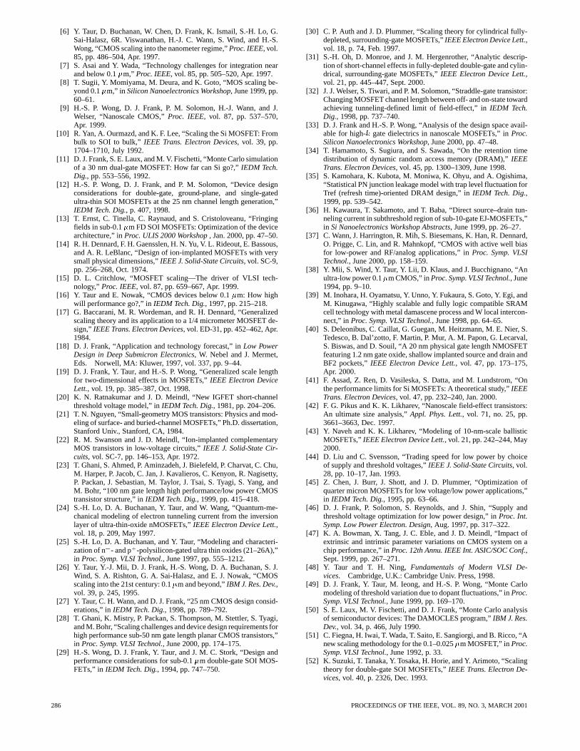
[6] Y. Taur, D. Buchanan, W. Chen, D. Frank, K. Ismail, S.-H. Lo, G.Sai-Halasz, 6R. Viswanathan, H.-J. C. Wann, S. Wind, and H.-S.Wong, “CMOS scaling into the nanometer regime,”Proc. IEEE, vol.85, pp. 486–504, Apr. 1997.
[7] S. Asai and Y. Wada, “Technology challenges for integration nearand below 0.1�m,” Proc. IEEE, vol. 85, pp. 505–520, Apr. 1997.
[8] T. Sugii, Y. Momiyama, M. Deura, and K. Goto, “MOS scaling be-yond 0.1�m,” in Silicon Nanoelectronics Workshop, June 1999, pp.60–61.
[9] H.-S. P. Wong, D. J. Frank, P. M. Solomon, H.-J. Wann, and J.Welser, “Nanoscale CMOS,”Proc. IEEE, vol. 87, pp. 537–570,Apr. 1999.
[10] R. Yan, A. Ourmazd, and K. F. Lee, “Scaling the Si MOSFET: Frombulk to SOI to bulk,” IEEE Trans. Electron Devices, vol. 39, pp.1704–1710, July 1992.
[11] D. J. Frank, S. E. Laux, and M. V. Fischetti, “Monte Carlo simulationof a 30 nm dual-gate MOSFET: How far can Si go?,”IEDM Tech.Dig., pp. 553–556, 1992.
[12] H.-S. P. Wong, D. J. Frank, and P. M. Solomon, “Device designconsiderations for double-gate, ground-plane, and single-gatedultra-thin SOI MOSFETs at the 25 nm channel length generation,”IEDM Tech. Dig., p. 407, 1998.
[13] T. Ernst, C. Tinella, C. Raynaud, and S. Cristoloveanu, “Fringingfields in sub-0.1�m FD SOI MOSFETs: Optimization of the devicearchitecture,” inProc. ULIS 2000 Workshop, Jan. 2000, pp. 47–50.
[14] R. H. Dennard, F. H. Gaensslen, H. N. Yu, V. L. Rideout, E. Bassous,and A. R. LeBlanc, “Design of ion-implanted MOSFETs with verysmall physical dimensions,”IEEE J. Solid-State Circuits, vol. SC-9,pp. 256–268, Oct. 1974.
[15] D. L. Critchlow, “MOSFET scaling—The driver of VLSI tech-nology,” Proc. IEEE, vol. 87, pp. 659–667, Apr. 1999.
[16] Y. Taur and E. Nowak, “CMOS devices below 0.1�m: How highwill performance go?,” inIEDM Tech. Dig., 1997, pp. 215–218.
[17] G. Baccarani, M. R. Wordeman, and R. H. Dennard, “Generalizedscaling theory and its application to a 1/4 micrometer MOSFET de-sign,” IEEE Trans. Electron Devices, vol. ED-31, pp. 452–462, Apr.1984.
[18] D. J. Frank, “Application and technology forecast,” inLow PowerDesign in Deep Submicron Electronics, W. Nebel and J. Mermet,Eds. Norwell, MA: Kluwer, 1997, vol. 337, pp. 9–44.
[19] D. J. Frank, Y. Taur, and H.-S. P. Wong, “Generalized scale lengthfor two-dimensional effects in MOSFETs,”IEEE Electron DeviceLett., vol. 19, pp. 385–387, Oct. 1998.
[20] K. N. Ratnakumar and J. D. Meindl, “New IGFET short-channelthreshold voltage model,” inIEDM Tech. Dig., 1981, pp. 204–206.
[21] T. N. Nguyen, “Small-geometry MOS transistors: Physics and mod-eling of surface- and buried-channel MOSFETs,” Ph.D. dissertation,Stanford Univ., Stanford, CA, 1984.
[22] R. M. Swanson and J. D. Meindl, “Ion-implanted complementaryMOS transistors in low-voltage circuits,”IEEE J. Solid-State Cir-cuits, vol. SC-7, pp. 146–153, Apr. 1972.
[23] T. Ghani, S. Ahmed, P. Aminzadeh, J. Bielefeld, P. Charvat, C. Chu,M. Harper, P. Jacob, C. Jan, J. Kavalieros, C. Kenyon, R. Nagisetty,P. Packan, J. Sebastian, M. Taylor, J. Tsai, S. Tyagi, S. Yang, andM. Bohr, “100 nm gate length high performance/low power CMOStransistor structure,” inIEDM Tech. Dig., 1999, pp. 415–418.
[24] S.-H. Lo, D. A. Buchanan, Y. Taur, and W. Wang, “Quantum-me-chanical modeling of electron tunneling current from the inversionlayer of ultra-thin-oxide nMOSFETs,”IEEE Electron Device Lett.,vol. 18, p. 209, May 1997.
[25] S.-H. Lo, D. A. Buchanan, and Y. Taur, “Modeling and characteri-zation of n - and p -polysilicon-gated ultra thin oxides (21–26A),”in Proc. Symp. VLSI Technol., June 1997, pp. 555–1212.
[26] Y. Taur, Y.-J. Mii, D. J. Frank, H.-S. Wong, D. A. Buchanan, S. J.Wind, S. A. Rishton, G. A. Sai-Halasz, and E. J. Nowak, “CMOSscaling into the 21st century: 0.1�m and beyond,”IBM J. Res. Dev.,vol. 39, p. 245, 1995.
[27] Y. Taur, C. H. Wann, and D. J. Frank, “25 nm CMOS design consid-erations,” inIEDM Tech. Dig., 1998, pp. 789–792.
[28] T. Ghani, K. Mistry, P. Packan, S. Thompson, M. Stettler, S. Tyagi,and M. Bohr, “Scaling challenges and device design requirements forhigh performance sub-50 nm gate length planar CMOS transistors,”in Proc. Symp. VLSI Technol., June 2000, pp. 174–175.
[29] H.-S. Wong, D. J. Frank, Y. Taur, and J. M. C. Stork, “Design andperformance considerations for sub-0.1�m double-gate SOI MOS-FETs,” in IEDM Tech. Dig., 1994, pp. 747–750.
[30] C. P. Auth and J. D. Plummer, “Scaling theory for cylindrical fully-depleted, surrounding-gate MOSFETs,”IEEE Electron Device Lett.,vol. 18, p. 74, Feb. 1997.
[31] S.-H. Oh, D. Monroe, and J. M. Hergenrother, “Analytic descrip-tion of short-channel effects in fully-depleted double-gate and cylin-drical, surrounding-gate MOSFETs,”IEEE Electron Device Lett.,vol. 21, pp. 445–447, Sept. 2000.
[32] J. J. Welser, S. Tiwari, and P. M. Solomon, “Straddle-gate transistor:Changing MOSFET channel length between off- and on-state towardachieving tunneling-defined limit of field-effect,” inIEDM Tech.Dig., 1998, pp. 737–740.
[33] D. J. Frank and H.-S. P. Wong, “Analysis of the design space avail-able for high-k gate dielectrics in nanoscale MOSFETs,” inProc.Silicon Nanoelectronics Workshop, June 2000, pp. 47–48.
[34] T. Hamamoto, S. Sugiura, and S. Sawada, “On the retention timedistribution of dynamic random access memory (DRAM),”IEEETrans. Electron Devices, vol. 45, pp. 1300–1309, June 1998.
[35] S. Kamohara, K. Kubota, M. Moniwa, K. Ohyu, and A. Ogishima,“Statistical PN junction leakage model with trap level fluctuation forTref (refresh time)-oriented DRAM design,” inIEDM Tech. Dig.,1999, pp. 539–542.
[36] H. Kawaura, T. Sakamoto, and T. Baba, “Direct source–drain tun-neling current in subthreshold region of sub-10-gate EJ-MOSFETs,”in Si Nanoelectronics Workshop Abstracts, June 1999, pp. 26–27.
[37] C. Wann, J. Harrington, R. Mih, S. Biesemans, K. Han, R. Dennard,O. Prigge, C. Lin, and R. Mahnkopf, “CMOS with active well biasfor low-power and RF/analog applications,” inProc. Symp. VLSITechnol., June 2000, pp. 158–159.
[38] Y. Mii, S. Wind, Y. Taur, Y. Lii, D. Klaus, and J. Bucchignano, “Anultra-low power 0.1�m CMOS,” inProc. Symp. VLSI Technol., June1994, pp. 9–10.
[39] M. Inohara, H. Oyamatsu, Y. Unno, Y. Fukaura, S. Goto, Y. Egi, andM. Kinugawa, “Highly scalable and fully logic compatible SRAMcell technology with metal damascene process and W local intercon-nect,” inProc. Symp. VLSI Technol., June 1998, pp. 64–65.
[40] S. Deleonibus, C. Caillat, G. Guegan, M. Heitzmann, M. E. Nier, S.Tedesco, B. Dal’zotto, F. Martin, P. Mur, A. M. Papon, G. Lecarval,S. Biswas, and D. Souil, “A 20 nm physical gate length NMOSFETfeaturing 1.2 nm gate oxide, shallow implanted source and drain andBF2 pockets,”IEEE Electron Device Lett., vol. 47, pp. 173–175,Apr. 2000.
[41] F. Assad, Z. Ren, D. Vasileska, S. Datta, and M. Lundstrom, “Onthe performance limits for Si MOSFETs: A theoretical study,”IEEETrans. Electron Devices, vol. 47, pp. 232–240, Jan. 2000.
[42] F. G. Pikus and K. K. Likharev, “Nanoscale field-effect transistors:An ultimate size analysis,”Appl. Phys. Lett., vol. 71, no. 25, pp.3661–3663, Dec. 1997.
[43] Y. Naveh and K. K. Likharev, “Modeling of 10-nm-scale ballisticMOSFETs,”IEEE Electron Device Lett., vol. 21, pp. 242–244, May2000.
[44] D. Liu and C. Svensson, “Trading speed for low power by choiceof supply and threshold voltages,”IEEE J. Solid-State Circuits, vol.28, pp. 10–17, Jan. 1993.
[45] Z. Chen, J. Burr, J. Shott, and J. D. Plummer, “Optimization ofquarter micron MOSFETs for low voltage/low power applications,”in IEDM Tech. Dig., 1995, pp. 63–66.
[46] D. J. Frank, P. Solomon, S. Reynolds, and J. Shin, “Supply andthreshold voltage optimization for low power design,” inProc. Int.Symp. Low Power Electron. Design, Aug. 1997, pp. 317–322.
[47] K. A. Bowman, X. Tang, J. C. Eble, and J. D. Meindl, “Impact ofextrinsic and intrinsic parameter variations on CMOS system on achip performance,” inProc. 12th Annu. IEEE Int. ASIC/SOC Conf.,Sept. 1999, pp. 267–271.
[48] Y. Taur and T. H. Ning,Fundamentals of Modern VLSI De-vices. Cambridge, U.K.: Cambridge Univ. Press, 1998.
[49] D. J. Frank, Y. Taur, M. Ieong, and H.-S. P. Wong, “Monte Carlomodeling of threshold variation due to dopant fluctuations,” inProc.Symp. VLSI Technol., June 1999, pp. 169–170.
[50] S. E. Laux, M. V. Fischetti, and D. J. Frank, “Monte Carlo analysisof semiconductor devices: The DAMOCLES program,”IBM J. Res.Dev., vol. 34, p. 466, July 1990.
[51] C. Fiegna, H. Iwai, T. Wada, T. Saito, E. Sangiorgi, and B. Ricco, “Anew scaling methodology for the 0.1–0.025�m MOSFET,” inProc.Symp. VLSI Technol., June 1992, p. 33.
[52] K. Suzuki, T. Tanaka, Y. Tosaka, H. Horie, and Y. Arimoto, “Scalingtheory for double-gate SOI MOSFETs,”IEEE Trans. Electron De-vices, vol. 40, p. 2326, Dec. 1993.
286 PROCEEDINGS OF THE IEEE, VOL. 89, NO. 3, MARCH 2001
[53] C. Kittel, Introduction to Solid State Physics. New York: Wiley,1956, ch. 11, p. 283.
[54] H.-S. P. Wong, “Novel device options for sub-100 nm CMOS,”in IEDM Short Course: Sub-100 nm CMOS, M. Bohr,Ed. Piscataway, NJ: IEEE Press, 1999.
[55] M. Ieong and H.-S. P. Wong, “Analysis of 25 nm double-gate MOS-FETs including self-consistent 2-D quantization effects,”IEEE Elec-tron Device Lett., submitted for publication.
[56] M. V. Fischetti, “A master equation approach to the study of elec-tronic transport in small semiconductor devices,”Phys. Rev. B, vol.59, no. 7, pp. 4901–4917, Feb. 1999.
[57] S. E. Laux and M. V. Fischetti, “Monte Carlo study of velocity over-shoot in switching a 0.1-micron CMOS inverter,” inIEDM Tech.Dig., 1997, pp. 877–880.
[58] F. Gamiz, J. A. Lopez-Villanueva, J. B. Roldan, J. E. Carceller, andP. Cartujo, “Monte Carlo simulation of electron transport propertiesin extremely thin SOI MOSFETs,”IEEE Trans. Electron Devices,vol. 45, pp. 1122–1126, May 1998.
[59] F. Gamiz, J. B. Roldan, P. Cartujo-Cassinello, J. E. Carceller, J.A. Lopez-Villanueva, and S. Rodriguez, “Electron mobility inextremely thin single-gate silicon-on-insulator inversion layers,”J.Appl. Phys., vol. 86, no. 11, pp. 6269–6275, 1999.
[60] M. Shoji and S. Horiguchi, “Electronic structures and phonon lim-ited electron mobility of double-gate silicon-on-insulator Si inver-sion layers,”J. Appl. Phys., vol. 85, no. 5, pp. 2722–2731, 1999.
[61] A. Toriumi, J. Koga, H. Satake, and A. Ohata, “Performance and re-liability concerns of ultra-thin SOI and ultra-thin gate oxide MOS-FETs,” in IEDM Tech. Dig., 1995, pp. 847–850.
[62] J.-H. Choi, Y.-J. Park, and H.-S. Min, “Electron mobility behaviorin extremely thin SOI MOSFETs,”IEEE Electron Device Lett., vol.16, pp. 527–529, Nov. 1995.
[63] T. Ernst, D. Munteanu, S. Cristoloveanu, T. Ouisse, S. Horiguchi, Y.Ono, Y. Takahashi, and K. Murase, “Investigation of SOI MOSFETswith ultimate thickness,”Microelectron. Eng., vol. 48, pp. 339–342,June 1999.
[64] H.-S. Wong, K. Chan, and Y. Taur, “Self-aligned (top and bottom)double-gate MOSFET with a 25 nm thick silicon channel,” inIEDMTech. Dig., 1997, pp. 427–430.
[65] D. Hisamoto, W.-C. Lee, J. Kedzierski, E. Anderson, H. Takeuchi,K. Asano, T.-J. King, J. Bokor, and C. Hu, “A folded-channelMOSFET for deep-sub-tenth micron era,” inIEDM Tech. Dig.,1998, pp. 1032–1034.
[66] X. Huang, W.-C. Lee, C. Ku, D. Hisamoto, L. Chang, J. Kedzierski,E. Anderson, H. Takeuchi, Y.-K. Choi, K. Asano, V. Subramanian,T.-J. King, J. Bokor, and C. Hu, “Sub 50-nm FinFET: PMOS,” inIEDM Tech. Dig., 1999, pp. 67–70.
[67] J.-H. Lee, G. Tarashi, A. Wei, T. A. Langdo, E. A. Fitzgerald, and D.A. Antoniadis, “Super self-aligned double-gate (SSDG) MOSFETsutilizing oxidation rate difference and selective epitaxy,” inIEDMTech. Dig., 1999, pp. 71–74.
[68] R. W. Keyes, “The effect of randomness in the distribution of im-purity atoms on FET thresholds,”Appl. Phys., vol. 8, pp. 251–259,1975.
[69] V. De, X. Tang, and J. Meindl, “Random MOSFET parameter fluc-tuation limits to gigascale integration (GSI),” inProc. Symp. VLSITechnol., June 1996, pp. 198–199.
[70] X. Tang, V. K. De, and J. D. Meindl, “Intrinsic MOSFET parameterfluctuations due to random dopant placement,”IEEE Trans. VLSISyst., vol. 5, pp. 369–376, Dec. 1997.
[71] V. K. De, X. Tang, and J. D. Meindl, “Scaling limits of Si MOSFETtechnology imposed by random parameter fluctuations,” inProc.IEEE Device Res. Conf. Dig., June 1996, pp. 114–115.
[72] Y. Yasuda, M. Takamiya, and T. Hiramoto, “Effects of impurity po-sition distribution on threshold voltage fluctuations in scaled MOS-FETs,” in Si Nanoelectronics Workshop Abstracts, June 1999, pp.26–27.
[73] H.-S. Wong and Y. Taur, “Three-dimensional ‘atomistic’ simula-tion of discrete microscopic random dopant distributions effects insub-0.1�m MOSFETs,” inIEDM Tech. Dig., 1993, pp. 705–708.
[74] H.-S. P. Wong, Y. Taur, and D. Frank, “Discrete random dopant dis-tribution effects in nanometer-scale MOSFETs,”Microelectron. Re-liability , vol. 38, no. 9, pp. 1447–1456, 1998.
[75] A. Asenov and S. Saini, “Random dopant fluctuation resistant de-canano MOSFET architectures,” inSi Nanoelectronics WorkshopAbstracts, June 1999, pp. 84–85.
[76] P. M. Solomon, “A comparison of semiconductor devices for highspeed logic,”Proc. IEEE, vol. 70, pp. 489–509, May 1982.
[77] A. Asenov, G. Slavcheva, A. R. Brown, J. H. Davies, and S. Saini,“Quantum mechanical enhancement of the random dopant inducedthreshold voltage fluctuations and lowering in sub 0.1 micron MOS-FETs,” in IEDM Tech. Dig., 1999, pp. 535–538.
[78] D. Burnett, K. Erington, C. Subramanian, and K. Baker, “Implica-tions of fundamental threshold voltage variations for high-densitySRAM and logic circuits,” inProc. Symp. VLSI Technol., June 1994,pp. 15–16.
[79] D. J. Frank and H.-S. P. Wong, “Simulation of stochastic doping ef-fects in Si MOSFETs,” inProc. Int. Workshop Computational Elec-tron., May 2000, pp. 2–3.
[80] D. B. Tuckerman and R. F. W. Pease, “High-performance heatsinking for VLSI,” IEEE Electron Device Lett., vol. EDL-2, pp.126–129, May 1981.
[81] D. J. Frank, “Design considerations for CMOS near the limits ofscaling,” inProc. ULIS 2000 Workshop, Jan. 2000, pp. 3–7.
[82] J. H. Stathis, A. Vayshenker, P. R. Varekamp, E. Y. Wu, C. Montrose,J. McKenna, D. J. DiMaria, L.-K. Han, E. Cartier, R. A. Wachnik,and B. P. Linder, “Breakdown measurements of ultra-thin SiOatlow voltage,” inProc. Symp. VLSI Technol., June 2000, pp. 94–95.
[83] R. H. Dennard, “Scaling challenges for DRAM and microprocessorsin the 21st century,” inProc. Int. Symp. ULSI Science Technol., 1997,pp. 519–532.
[84] M. Asakuraet al., “A 34 nm 256 Mb DRAM with boosted sense-ground scheme,” inInt. Solid State Circuits Conf., Dig. Tech. Papers,1994, pp. 140–141.
[85] J. Chen, T. Y. Chan, I. C. Chen, P. K. Ko, and C. Hu, “Sub-breakdowndrain leakage current in MOSFET,”IEEE Electron Device Lett., vol.EDL-8, pp. 515–518, Nov. 1987.
[86] Grueninget al., “A novel trench DRAM cell with a VERtIcal accesstransistor and BuriEd STrap (VERI BEST) for 4 Gb/16Gb,” inIEDMTech. Dig., 1999, pp. 25–28.
[87] O. Takahashi, S. Dhong, M. Ohkubo, S. Onishi, R. Dennard, R.Hannon, S. Crowder, S. Iyer, M. Wordeman, B. Davari, W. B. Wein-berger, and N. Aoki, “1 GHz fully pipelined 3.7 ns address accesstime 8K� 1024 embedded DRAM macro,” inProc. Int. Solid StateCircuits Conf., Feb. 2000, pp. 396–397.
[88] D. R. Bearden, D. G. Caffo, P. Anderson, P. Rossbach, N. Iyengar, T.A. Petersen, and J.-T. Yen, “A 780 MHz PowerPC microprocessorwith integrated L2 cache,” inProc. Int. Solid State Circuits Conf.,Feb. 2000, pp. 90–91.
[89] F. Nemati and J. D. Plummer, “A novel thyristor-based SRAM cell(T-RAM) for high-speed, low-voltage, giga-scale memories,” inIEDM Tech. Dig., 1999, pp. 283–289.
[90] C. Lage, J. D. Hayden, and C. Subramanian, “Advanced SRAM tech-nology—The race between 4T and 6T cells,” inIEDM Tech. Dig.,1996, pp. 271–272.
[91] K. Itoh, A. R. Fridi, A. Bellaouar, and M. I. Elmasry, “Deep sub-V,single power-supply SRAM cell with multiV , bosted storage nodeand dynamic load,” inProc. Symp. VLSI Technology, June 1996, pp.132–133.
[92] A. R. Fridi, P. M. Solomon, D. J. Frank, S. Reynolds, D. Pearson, andM. I. Elmasry, “A 0.22�m CMOS 0.65 V 500 MHz 64 Kb SRAMmacro,”, unpublished, 1998.
[93] T. H. Meng, B. M. Gordon, E. K. Tsern, and A. C. Hung, “Portablevideo-on-demand in wireless communication,”Proc. IEEE, vol. 83,pp. 359–380, Apr. 1995.
[94] D. Cheseboro, J. Adkinson, L. Clark, S. Eslinger, M. Faucher, S.Holmes, R. Mallette, E. Nowak, E. Sengele, S. Voldman, and T.Weeks, “Overview of gate linewidth control in the manufacture ofCMOS logic chips,”IBM J. Res. Dev., vol. 39, no. 1/2, pp. 198–200,1995.
[95] L. Suet al., “A high performance 0.08�m CMOS,” inProc. Symp.VLSI Technology, June 1996, p. 12.
[96] Y. Yang et al., “Sub-60 nm physical gate length SOI CMOS,” inIEDM Tech. Dig., 1999, pp. 431–434.
[97] J. R. Brews, “Physics of the MOS transistor,” inApplied Solid StateScience. New York: Academic, 1981, pp. 1–120.
FRANK et al.: DEVICE SCALING LIMITS OF Si MOSFETs AND THEIR APPLICATION DEPENDENCIES 287

David J. Frank (Member, IEEE) received theB.S. degree from the California Institute ofTechnology, Pasadena, in 1977, and the Ph.D.degree in physics from Harvard University,Cambridge, MA, in 1983.
He is currently with the IBM T. J. WatsonResearch Center, Yorktown Heights, NY, wherehe is a Research Staff Member. He has servedon technical program committees for the Inter-national Electron Devices Meeting and the SiNanoelectronics Workshop. He has authored
or coauthored over 70 technical publications and holds six U.S. Patents.His studies and recent work include nonequilibrium superconductivity,modeling and measuring III–V devices, exploring the limits of scalingof silicon technology, the modeling of innovative Si devices, analysis ofCMOS scaling issues such as discrete dopant effects and short-channeleffects associated with high-k gate insulators, investigating the usefulnessof energy-recovering CMOS logic and reversible computing concepts, andlow-power circuit design. His research interests include superconductorand semiconductor device physics, modeling and measurement, circuitdesign, and percolation in two-dimensional systems.
Robert H. Dennard (Fellow, IEEE) was bornin Terrell, TX, in 1932. He received the B.S.and M.S. degrees in electrical engineering fromSouthern Methodist University, Dallas, TX, in1954 and 1956, respectively, and the Ph.D. de-gree from the Carnegie Institute of Technology,Pittsburgh, PA, in 1958.
He then joined IBM Research Division, wherehis early experience includes the study of new de-vices and circuits for logic and memory applica-tions and the development of advanced data com-
munication techniques. Since 1963, he has been with the IBM Thomas J.Watson Research Center, Yorktown Heights, NY, where he has been in-volved in microelectronics research and development. His primary researchinterests has been in MOSFETs and integrated digital circuits that use them.In 1967, he invented the dynamic RAM memory cell used in most computerstoday. With others, he developed the concept of MOSFET scaling in 1972.
Dr. Dennard was appointed an IBM Fellow in 1979 and was elected tothe National Academy of Engineering in 1984. He was inducted into the Na-tional Inventors Hall of Fame and became a Member of the American Philo-sophical Society in 1997. He received the IEEE Cledo Brunetti Award in1982, the National Medal of Technology from President Reagan in 1988 forhis invention of the one-transistor dynamic memory cell, the IRI Achieve-ment Award from the Industrial Research Institute in 1989, and the HarveyPrize from Technion, Haifa, Israel, in 1990.
Edward Nowak (Member, IEEE) received theB.S. degree in physics from the MassachusettsInstitute of Technology, Cambridge, in 1973,and the M.S. and Ph.D. degrees from the particletheory group at the University of Maryland,College Park, in 1974 and 1978, respectively.
Following post-doctoral research at New YorkUniversity, he joined IBM’s technology develop-ment group, Essex Junction, VT, to work on 1-MbDRAM, and then began work on sub-half-micronMOSFETs for logic in 1984. He has contributed
to numerous high-speed CMOS projects from 1.0-�m to 0.1-�m scales. Heinvented on 32 U.S. patents in the areas of CMOS circuits, devices and pro-cesses, and has authored numerous papers in these areas. He is currentlyengaged in the pursuit of sub-one-volt device designs and continues workon high-speed CMOS device design.
Paul M. Solomon(Fellow, IEEE) was born in Cape Town, South Africa. Hereceived the B.Sc. degree in electrical engineering from the University ofCape Town, South Africa, in 1968 and the Ph.D. degree from the Technion,Haifa, Israel, in 1974.
Since 1975, he has been a Research Staff Member at the I.B.M. T. J.Watson Research Center, Yorktown Heights, NY, where his interests havebeen in the field of high-speed semiconductor devices. He has contributedto the physics of transport in semiconductors and has taught the physics ofhigh-speed devices at Stanford University, Stanford, CA. He has also con-tributed to the theory of scaling bipolar transistors to very small dimensionsand has developed methodologies to compare the performance of high-speedsemiconductor devices. The design of high-speed semiconductor logic de-vices has been a continuing topic, ranging from self-aligned bipolar transis-tors through novel heterostructure field effect transistors and, more recently,to novel CMOS device concepts.
Dr. Solomon is a Member of the APS.
Yuan Taur (Fellow, IEEE) received the B.S. de-gree in physics from National Taiwan University,Taipei, Taiwan, R.O.C., in 1967 and the Ph.D.degree in physics from University of California,Berkeley, in 1974.
From 1975 to 1979, he was with NASA, God-dard Institute for Space Studies, NY, workingon low-noise Josephson junction mixers formillimeter-wave detection. From 1979 to 1981,he was with Rockwell International ScienceCenter, Thousand Oaks, CA, working on II–VI
semiconductor devices for infrared sensor applications. Since 1981, hehas been with the Silicon Technology Department of IBM Thomas J.Watson Research Center, Yorktown Heights, NY, where he was Managerof Exploratory Devices and Processes. He has served on the technicalprogram committees and as a Panelist at the Device Research Conference,International Electron Device Meeting, and as Rump Session Chairmanand Secretary at the Symposium on VLSI Technology. His recent workincludes Latchup-free 1-�m CMOS, self-aligned TiSi2, 0.5-um CMOSand BiCMOS, shallow trench isolation, 0.25-�m CMOS with n /ppoly gates, SOI, low-temperature CMOS, and 0.1-�m CMOS. He hasauthored or coauthored over 100 technical papers, holds 10 U.S. patents,and coauthoredFundamentals of Modern VLSI Devices(Cambridge, U.K.:Cambridge Univ. Press, 1998).
Dr. Taur is the Editor-in-Chief of the IEEE ELECTRONDEVICE LETTERS.He received four Outstanding Technical Achievement Awards and six In-vention Achievement Awards during his IBM career.
Hon-Sum Philip Wong (Senior Member, IEEE)received the B.Sc. degree from the University ofHong Kong in 1982 and the Ph.D. degree in elec-trical engineering from Lehigh University, Beth-lehem, PA, in 1988.
He joined the IBM Thomas J. WatsonResearch Center, Yorktown Heights, NY, in1988, where he is now Senior Manager of theExploratory Devices and Integration TechnologyDepartment. Since 1993, he has been workingon device physics, fabrication, and applications
of nanoscale CMOS devices. His recent work has been on the physics andfabrication technology of double-gate and back-gate MOSFETs for CMOStechnologies toward the 25-nm channel length regime. In 1997, he reportedthe first successful fabrication of a self-aligned double-gate MOSFET usinga pattern-constrained selective epitaxial growth technique. In the applica-tions arena, his work has been on solid-state imaging. His recent work hasbeen imaging devices using CMOS technologies. From 1988 to 1992, heworked on the design, fabrication, and characterization of a high-resolution,high-color–fidelity CCD image scanner for art work archiving. Thesescanners are now in use at several premier museums around the world. Hisresearch interests have been in electron device physics, device simulationand modeling, microelectronics fabrication technology, applications ofmicroelectronic systems, and solid-state imagers.
Dr. Wong serves on the IEEE Electron Devices Society as Chair of theVLSI Circuits and Technology Committee and a Member of the PublicationCommittee.
288 PROCEEDINGS OF THE IEEE, VOL. 89, NO. 3, MARCH 2001