cloud data center acceleration - memcon 2016 · 7 emerging: data stream mining, real time analytics...
TRANSCRIPT

Cloud Data Center Acceleration 2015

Agenda
2
! Computer & Storage Trends ! Server and Storage System
- Memory and Homogenous Architecture - Direct Attachment
! Memory Trends ! Acceleration Introduction ! FPGA Adoption Examples

Server (Computer) & Storage Trends
! Cloud computing, virtualization, convergence - Server & storage consolidation & virtualization - Convergence to PCIe backplane and low latency 25GbE - Distributed storage and cache for cloud computing - Convergence is enabling lower power and higher density
! Lots of interest in Storage, Storage Class Memory - Capacity Expansion - DRAM to flash, and flash cache - Intermediate Storage - Disaggregation of Storage and Data - Rapid change & new cloud architectures - “Verticalization”, disaggregation, dense computing for cloud servers - Acceleration option with FPGA per node, or pool heterogeneous accelerators
3

Data Center Challenges
! Memory & IO bottlenecks limit utilization - Typical server workloads run at ~20% processor utilization
! Virtualization driving application consolidation - But memory and IO are limiting factors to better utilization
- “Big Data” configurations are also bottlenecked ! Especially search and analytics workloads
! The Processor mostly waits for RAM - Flash / Disk are100,000 …1,000,000 clocks away from cpu - RAM is ~100 clocks away unless you have locality (cache). - If you want 1CPI (clock per instruction) you have to have the data in cache
(program cache is “easy” ) - This requires cache conscious data-structures and algorithms sequential (or
predictable) access patterns - In Memory DB is going to be common (SPARK Architecture)
Source: Microsoft 4
FPGA
CPU A

O/S Bypass: DMA, RDMA, zero copy, cpu cache direct
5
! Avoid memory copies ! NICs, clusters, accelerators ! DMA, RDMA
– Mellanox RoCE, Infiniband
! Intel PCIe steering hints – Into cpu cache
! Heterogeneous System Architecture (HSA) – For accelerators
! Direct Access to cpu cache – QPI, CAPI – Low latency – Simplified programming model – Huge benefit for flash cache

Computing Bottlenecks ! Memory bottleneck
- Need faster & larger DRAM ! CPU core growth > memory b/w ! CPU has limited # of pins ! DRAM process geometry limits
- Emerging: ! Stacked DRAM in package ! Optics from CPU package ! Optics controller for clusters
! Cluster networking ! Over optics
! Main Storage Data response time - Impact Big Data Processing
6
In Optics Controller w/switching
Optics Controller to TOR

7
Emerging: Data Stream Mining, Real Time Analytics
! Data stream examples – Computer network traffic – Data feeds – Sensor data
! Benefits – Real time analytics
! Predict class or value of new instances ! e.g. security threats with machine learning
– Filtering data to store
! Topology – Single or Multiple FPGA accelerators

• Did the 14nm NAND delay drive these solutions to becomes next gen?
• Or did the need for more flexible memory and storage applications Drive this transition?
• New Memories are complementary to existing solutions
• How to Adopt • Where do they go
• How do they fit in tomorrows Server/storage Architectures
8
Enter New Memory solutions (A new Dawn Awaits)

3D XPoint vs. NAND
9
! 1000X faster write ! Much better endurance ! 5X to 7X Faster SSD’s ! Cost & Price in between DRAM and flash ! Altera FPGA controller options

Rapid Change in the Cloud Data Center
10
! Rapid change & new cloud architectures - “Verticalization”, disaggregation, dense computing for cloud servers - Intel offering 35 custom Xeons for Grantley - Software Defined Data Center
! Pool resources (compute, network, storage), automate provisioning, monitoring - Intel MCM & Microsoft Bing FPGA announcements - Intel Standard to Custom Roadmap showing 35 Grantley SKU’s:

11
Accelerator Spectrum
Database Graph Numeric Computing
Machine Learning
Image Pattern Recognition Computational Medical
Diagnosis Data
Streaming Best match
Engines
Data Analytics Computer Vision
Search Ranking
Visual Analytics
Language Proc.
Alg
orith
ms
Application Spectrum
12
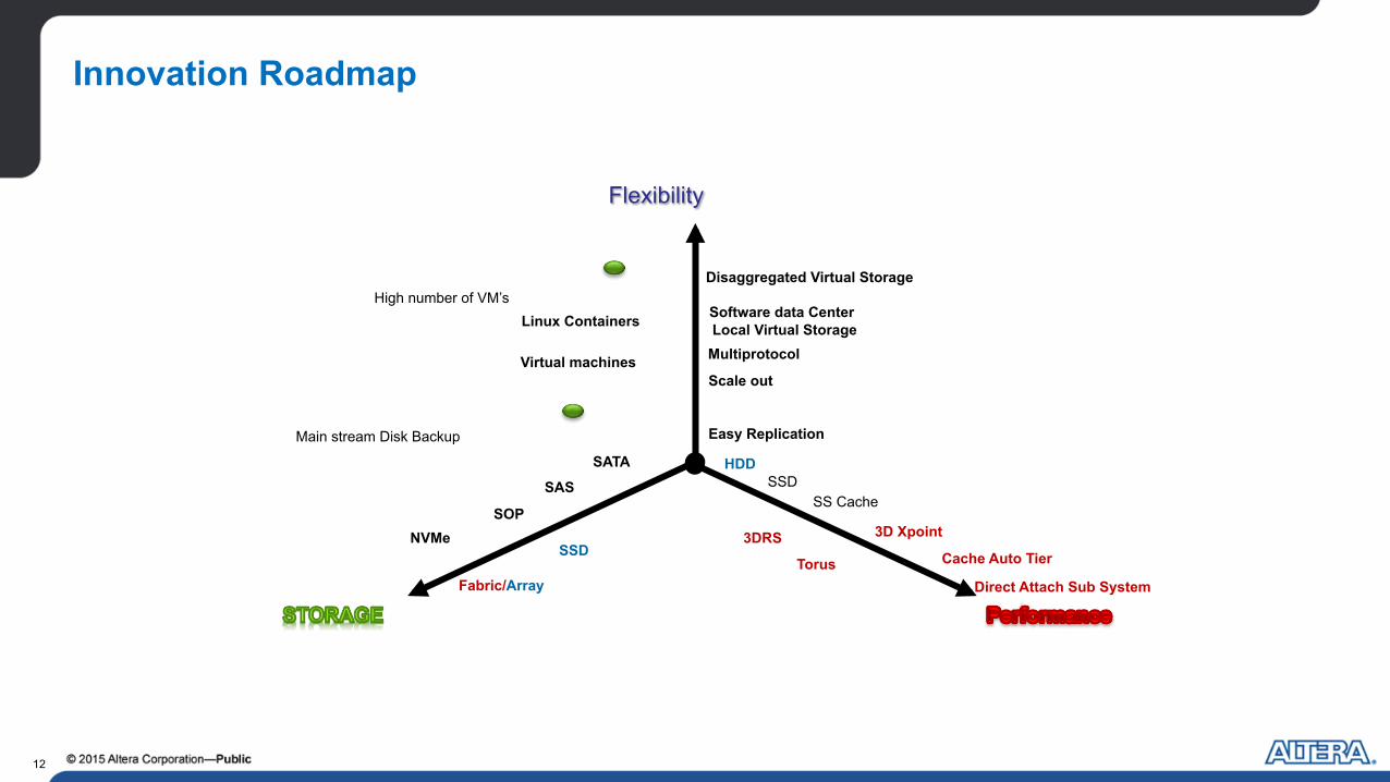
Innovation Roadmap
Flexibility
Direct Attach Sub System
3DRS Cache Auto Tier
SS Cache SSD
SSD
HDD
NVMe SOP
SAS
SATA
Linux Containers Software data Center
Easy Replication
Multiprotocol
Fabric/Array
Torus
3D Xpoint
Scale out
High number of VM’s
Main stream Disk Backup
Local Virtual Storage
Disaggregated Virtual Storage
Virtual machines

Small processors close to storage e.g Map Function
Efficient Data Centric Computing Topologies
P1
Pn-1
Pn
Flash Drive(s)
Memory
Memory
Memory
Flash Drive(s)
Flash Drive(s)
Switch or/and Large Aggregating
Processor
e.g. map result collection and Reduce Function
Network Attach
Server with Unstructured Search Topology – e.g. Hadoop + Map/
Reduce
Server with 3D Torus Configurations
X TFlop Processor X TBytes Memory
X TB/s
Server with Balanced FLOPs/Byte/s and FLOPs/Byte Depth
P1
Server With Multi Node Pipeline
Pn-1 Pn
130 GB Memory 130 GB Memory 130 GB Memory
Network / Storage Attach
Network / Storage Attach
Application : Data Analytics / Data Search / Video Server Application : Large Dataset HPC with Compute intensive function that
do not scale well – e.g.FEA
Application : Classic HPC, e.g. QCD, CFD, Weather
Modeling
Application : Deep Pipeline DSP, e.g. Video Analytics
Network / Storage Attach

14
Microsoft SmartNIC with FPGA for Azure (8-25-15 Hot Chips Presentation)
! Scaling up to 40 Gbs and beyond
– Requires significant computation for packet processing ! Use FPGAs for reconfigurable functions
– Already used in Bing – SW Configurable
! Program with Generic Flow Tables (GFT) – SDN i/f to hardware
! SmartNIC also does Crypto, QoS, storage acceleration, and more…
http://tinyurl.com/p4sghaq

FPGA AlexNet Classification Demo (Intel IDF, August 2015)
! CNN AlexNet Classification - 2X+ Performance/W vs cpu (Arria 10) - 5X+ performance Arria 10 à Startix 10
! 3X DSP blocks, 2X clock speed
! Microsoft Projection - 880 images/s for A10GX115 - 2X Perf./W versus GPU
! Altera OpenCL AlexNet Example - 600+ images/s for A10GX115 by year end
15
CNN Classification Platform Power (W)
Performance (image/s)
Efficiency (Images/sec/W)
E52699 Dual Xeon Processor (18 cores per Xeon) 321 1320 4.11
PCIe w/ dual Arria 10 1150 130* 1200 9.27
AlexNet
Note *: CPU low power state of 65W included.

Why Expansion Memory?
Enable memory-intensive
computation
data exploration
statistics
machine learning
Big Data
graph-based informatics
...
Increase users’
productivity
algorithm expression
interactivity
Load Balancing
ISV apps
high-productivity languages
…
Change the way we look at data
Boost scientific output Broaden participation

Advanced memory controller market Memory innovation will change how computing is done
17
! Emerging market for “Advanced Memory Controllers”. – These devices interface to the processor by directly attaching to their existing memory interface
bus. – Memory Types will require New Controller implementations
! Memory offload Applications – Filtering, Acceleration, Capacity, Sub-Systems
! FPGA can translate between existing memory interface electricals and a plethora of backend devices, interfaces, or protocols to enable a wide variety of applications.
– Initial examples of this include: • Bridging between DDR4 and other memory technologies such as NAND Flash, MRAM, or
Memristor. • Memory depth expansion to enable up to 8X the memory density available per memory
controller. • Enable new memory adoption quickly • Enable acceleration of data processing for analytics applications • Enable offload of data management functions such as compression or encryption.

Application: DDR4 DIMM Replacement - Memory Bridging and/or In-line Acceleration
18
XEON
DD
R4
CTR
L
DD
R4
Slo
t 0
DD
R4
Slo
t 1
FPGA
Mem
ory,
3D
RS
: DD
R4,
N
AN
D, M
RA
M, M
emris
tor,
etc.
AD
V M
EM
CTR
L
DD
R4
Sla
ve
On- Chip Cache
Ctrl/Accel Logic
DIMM Module
Key Memory Attributes • Capacity
• Sub System mixed Memory • Optimized Solution for App
• Database Acceleration
On-Chip Cache
Memory Filter/Search

Acceleration Solutions
Data making money the new Way

Acceleration Memory Applications
20
Accelerator Application Memory Function Memory Type Future
Data Analytics Temporary Storage DDR3/4 Storage Class, HBM, HMC
Computer Vision/OCR Buffer DDR3/4 Storage Class
Image Pattern Recognition Storage, Buffer SSD, DDR Storage Class, HBM, HMC
Search Ranking storage, Working DDR3 Storage Class
Visual Analytics Buffer DDR3 Storage Class
Medical Imaging Storage, Buffer SSD, DDR3/4 Storage Class, DDR4,
• As FLOPs increase Memory Bandwidth will need to scale • As Data increases capacity will also increase to sustain computation

Accelerator Board Block Diagram
21
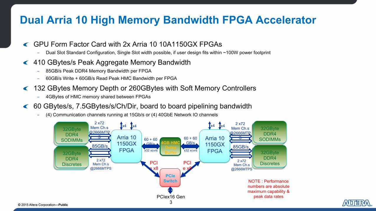
Dual Arria 10 High Memory Bandwidth FPGA Accelerator
! GPU Form Factor Card with 2x Arria 10 10A1150GX FPGAs - Dual Slot Standard Configuration, Single Slot width possible, if user design fits within ~100W power footprint
! 410 GBytes/s Peak Aggregate Memory Bandwidth - 85GB/s Peak DDR4 Memory Bandwidth per FPGA - 60GB/s Write + 60GB/s Read Peak HMC Bandwidth per FPGA
! 132 GBytes Memory Depth or 260GBytes with Soft Memory Controllers - 4GBytes of HMC memory shared between FPGAs
! 60 GBytes/s, 7.5GBytes/s/Ch/Dir, board to board pipelining bandwidth - (4) Communication channels running at 15Gb/s or (4) 40GbE Network IO channels
x32 xcvrs x32 xcvrs
Arria 10 1150GX FPGA
32GByte DDR4
SODIMMs Arria 10 1150GX FPGA
PCIex16 Gen 3
PCIe x8
PCIe x8
4GB HMC Delay Buffer
60 + 60 GB/s
60 + 60 GB/s
NOTE : Performance numbers are absolute maximum capability &
peak data rates
32GByte DDR4
Discretes
2 x72 Mem Ch.s
@2666MTPS
85GB/s
2 x72 Mem Ch.s
@2666MTPS
2 x72 Mem Ch.s
@2666MTPS
85GB/s
2 x72 Mem Ch.s
@2666MTPS
32GByte DDR4
SODIMMs
32GByte DDR4
Discretes
PCIe Switch
x4 x4 x4 x4

Dual Stratix 10 3D Torus Scalable FPGA Accelerator
23
! GPU Form Factor Card with 2x Stratix 10 FPGAs - Support Majority of Stratix 10 Family – Both large and small devices from 2 to 10 TFlops
! 204 GBytes/s Peak Aggregate Memory Bandwidth - 102GB/s Peak DDR4 Memory Bandwidth per FPGA
! 256 GBytes Memory Depth ! 336 GBytes/s, 14GBytes/s/Channel/Direction, board to board Scaling
23
x8 xcvrs
Stratix 10 FPGA
32GByte DDR4
SODIMMs Stratix 10 FPGA
PCIex16 Gen 3
PCIe
x16
PCIe
x16
x4
Board to Board scaling Interconnect for 2D/3D Mesh/Torus Topologies
NOTE : Performance numbers are absolute maximum capability &
peak data rates
32GByte DDR4
Discretes
2 x72 Mem Ch.s
@3200MTPS
102GB/s
2 x72 Mem Ch.s @3200MTP
S
2 x72 Mem Ch.s
@3200MTPS
102GB/s
2 x72 Mem Ch.s @3200MTP
S
32GByte DDR4
SODIMMs
32GByte DDR4
Discretes
PCIe Switch
x4 x4 x4 x4 x4 x4 x4 x4 x4 x4 x4

Minimise Multiple accesses to External Memory
Function A
Function B
Iterate many times
Result read from p & q buffers after many
thousands of iterations
P Q
Access entire volume data storage in system memory
Global memory Global memory
Global memory
Global memory
Global memory Global memory
Function C
Traditional CPU/GPU Implementation
Function D
Function E
Global memory

Function E
Function D
Function C
Minimise Multiple accesses to External Memory
Function A
Function B
Iterate many times
Result read from p & q buffers after many
thousands of iterations
P Q
Access entire volume data storage in system memory
Global memory Global memory
Global memory
Traditional CPU/GPU Implementation
Global memory
Global memory
Global memory
Global memory

Function E
Function D
Function C
Minimise Multiple accesses to External Memory
Function A
Function B
Iterate many
times
Result read from p & q buffers after many
thousands of iterations
P Q
Access entire volume data storage in system memory
Global memory Global memory
Global memory
FPGA Implementation
D E E P P
P
L
I
E
I N
E
E
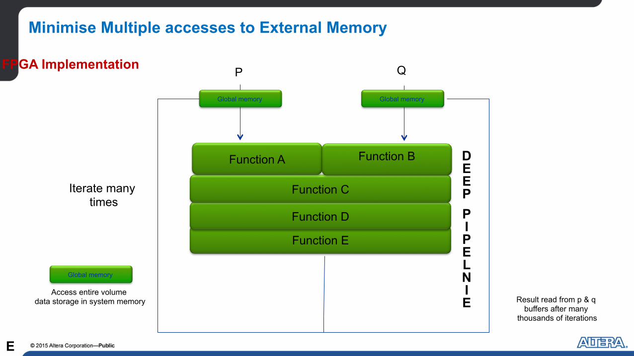

Function E
Function D
Function C
Try to Minimise Multiple accesses to External Memory
Function A
Function B
Iterate many
times
Result read from p & q buffers after many
thousands of iterations
P Q
Access entire volume data storage in system memory
Global memory Global memory
Global memory
FPGA Implementation
D E E P P
P
L
I
E
I N
E
E
Delay Line External Memory
Delay Line
Deeper than blockram when large algorithm data alignment is
required to further extend the deep pipeline
Summary
29
! FPGA utilizes less external memory bandwidth for Reverse Time Migration, CNN and other common acceleration algorithms.
! The growth in data and TFLOPs for Acceleration will require more BW and in a orderly fashion. New Memories will require higher bandwidth and controller changes.
! Memory and System solution to increase compute efficiency are changing architectures, networks and the type of memory.

30