clock tree optimization for power supply noise reduction · 2015-01-12 · 1 clock-tree...
TRANSCRIPT

Faculty of EngineeringBAR ILAN UNIVERSITY, Israel
Computer Engineering
Clock Tree Optimization for Power SupplyNoise Reduction
Yaakov Kaplan and Shmuel Wimer
Yaakov Kaplan and Shmuel Wimer
CE Tech Report # 001CE Tech Report # 001
Based on Bar Ilan MSc. Thesis of Y. Kaplan, supervised by S. Wimer
Jan. 12, 2015

1
Clock-Tree Optimization for Power Supply Noise Reduction
Yaakov Kaplan1,2
and Shmuel Wimer1
Abstract
The voltage drop incurred by the power supply in today’s VLSI chips is a major concern, known
as power supply noise. In sub-1volt supply voltage, noise of very few hundred millivolts causes
circuit malfunction. The reason for power supply noise is the fast and simultaneous voltage
switching. While the logic signal switching is spread across the entire clock cycle, the switching
of the clock-tree and the sequential circuits is occurring simultaneously, causing high current
peaks. The latter is a primary contributor to the power supply noise.
This work proposes to spread the switching of clock-tree drivers in an attempt to reduce the peak
current, while maintaining the clock signal quality and low skew at the far end tree’s leaves,
where the sequential circuits are connected. A methodology of driver switching characterization
has been developed for fast computation of peak current and other signal parameters, integrated
into a two-phase optimization algorithm. It first initializes the clock-tree in a top-down traversal,
employing a mix of high-threshold voltage (HVT) and low-threshold voltage (LVT) clock-
drivers tree branches. A bottom-up delay correction phase then takes place, aiming at clock skew
nullifying. The algorithm was implemented in 40 nanometers process technology, achieving a
reduction of 50% of the clock-tree peak current. The proposed method can be easily combined
with other existing methods to further reduce the peak current.
1. Introduction
The voltage drop incurred by the power supply in today’s VLSI chips is a major concern known
as power noise [1]. With the increase of design complexity, moving from Application Specific
Integrated Circuits (ASIC) to System on a Chip (SoC), and due to the sub-1volt supply voltage,
noise of very few hundreds millivolts causes circuit malfunction [2].
The fluctuations occurring in the high power supply ddV and the low power supply gndV voltages
are escalated by the process technology scaling. There, the underlying resistance, capacitance
and peak current are increasing, and the current switching becomes faster, namely dI dt grows
up, thus increasing the power noise. A typical model of power delivery network is illustrated in
Fig. 1 [1].
The network consists of a power supply located on the board, power consumers (system’s logic
circuits), and power and ground supply network (PDN). The power supply is assumed to behave
as an ideal voltage source providing nominal ddV and gndV . The power consumers are modeled
1 Bar-Ilan University, Engineering Faculty, Ramat-Gan, Israel
2 Apache Corp.

2
as time-dependent current sources, denoted by I t . ddV and gndV lines connecting the supply
with the power consumers are not ideal, having non-zero parasitic resistance pR and gR , and
inductance pL and gL , respectively. The resistive voltage drops is p g I R R , while the
inductive voltage drops is p g L L dI dt . Shown in Fig. 1, the high and low voltages are
therefore
dd p pV I R L dI dt , (1)
gnd g gV I R L dI dt . (2)
Figure 1: Non ideal power delivery network [1].
Ordinary logic and sequential circuits are designed to work in nominal power supply voltage.
Unfortunately maintaining constant voltage during operation is practically impossible. It all
comes to the simple Ohm low of multiplying peak current by the power network impedance. The
power network is an RLC circuit and high current peaks will thus cause various voltage drops at
various points of the network. The noise can therefore be reduced by lowering the impedance, or
avoiding high current peaks. Constructing proper power supply network having low-resistance
and inductance, and high capacitance has been treated by many research papers [3-5], and its
discussion is beyond the scope of this work, focusing on reducing the peak current.
Power noise can be controlled by reducing the PDN parasitic resistance R and inductance L , and
by lowering the current I and its density dI dt . Both techniques were extensively studied in the
literature. In [4] PDN parasitic resistance and inductance reduction were studied. In [6] it was
proposed to employ decoupling capacitors, hence reducing the effective R and L (and also the
resonance factors). The reduction of dI dt is obtained by improving the current sources. That
can also be achieved by decoupling capacitors (though the reduction mechanism is different).
Peak current reduction achieves the following goals.
1. Reduction of the on-die IR drop, where the resistance dominates the impedance.
2. Reduction of the L dI dt term occurring at the package level, where the inductance factor
dominates the impedance.

3
3. Reduction of the clock jitter which is directly affected by IR drop [7].
4. Improving the utilization of the de-coupling capacitors by increasing the effective distance of
the capacitors, that is inversely proportional to dI dt [6].
The clock related voltage switching is the primary contributor to power supply noise [8]. While
the logic signal switching is spread across the entire clock cycle, the switching of the clock-tree
and the sequential circuits is occurring simultaneously, causing high current peaks. The clock
network is therefore a natural candidate to treat for reducing peak current. A well-structured
clock-tree should deliver high quality clock signal to the underlying sequential circuits connected
at the tree’s leaves. To obtain proper and robust sequencing of the logic, the clock skew must
stay within prescribed limits, usually not exceeding 5% of the clock cycle [9]. To ensure fast
switching of the logic, the slope of the signal at tree’s leaves must also be sufficiently small.
Reducing the power supply peak current by clock-tree treatment is therefore a delicate task that
must be handled carefully to ensure clock signal integrity. For that, three approaches have been
proposed in the literature.
The first aims at reducing the power network impedance. Though it does not change the peak
current, the voltage drop does reduce. This approach comprises well established techniques such
as reducing the resistance of the power network by widening the power rails, increasing their
density, and extensive usage of vias. Another technique is using decoupling capacitors, to
effectively shorten the distance of the current sinks from their sources. Such techniques are being
used since the early days of VLSI design. An excellent review of those methods is found in [6].
A second technique [10] proposed to reduce the peak current by minimizing its component
caused by the flip-flops (FFs) switching. Its underlying idea is illustrated in Fig. 2. In (a) the
clock signals of the FFs are aligned, causing a large and narrow supply current pulse, compared
to (b) where the clock signals are displaced, and the resulting current pulse is smaller and spread
over time. To account for the peak current, the signal switching [10] accounted only the first
level of the combinational logic, assuming that the switching factor at deeper levels is far smaller
than at the first level. Peak current reduction was achieved by clock scheduling procedure which
utilized the allowable clock skew, a technique first proposed for timing optimization in a seminal
paper [11]. Clock signal rescheduling at FFs’ clock inputs may considerably complicate the
timing convergence of the underlying design. Peak current minimization by [10] could not be
handled by the linear programming solution used in [11], and a heuristic based on genetic
algorithm was proposed, yielding 30% of FFs peak current reduction, without sacrificing the
clock frequency.
A refinement of [10] was presented in [8], which accounted all the switching of deeper logic
levels. A more modest, but still significant peak current reduction of 12% was claimed, which
lead to 19% reduction of the power supply voltage variation. A heuristic to enhance the quality
of the genetic algorithm solution was presented in [12]. Paper [13] presents another skew
spreading optimization technique by dividing the skew time intervals into slots and then the

4
clock timing of each FF was allocated to some slot in an attempt to reduce the peak current. 17%
peak current reduction was claimed.
Figure 2: Peak supply current reduction by misalignment of the clock signal.
All the above works used current profiling of the gates involved in the combinational logic.
While [10] and [12] required full current characterization of the logic gates involved and thus
employed extensive SPICE simulations, [8] used only the peak current of those gates, making the
CAD solution simpler and easier to maintain on the account of accuracy. All those methods
approximated the current waveforms by triangles, which were scheduled according to the
switching time of their corresponding gates (see Fig. 2). The entire current profile drawn from
the power supply was obtained by a superposition of the individual current profiles. Our work
uses similar current profile methodology with full SPICE characterization. For our work SPICE
accuracy is essential since unlike the above mentioned methods, we pursue zero-skew.
As in [8,10,12,13], our work is flattening the peak supply current by manipulating the timing of
the clock signal. There is a major difference though, which avoids the timing side effects
difficulties mentioned before. While the former methods shift the clock signal at the far-end of
its distribution network, as shown in Fig. 2, our method does so only at the internal nodes of the
clock-tree, while the skew at the its far-end nodes is fully controlled and maintained small.
Furthermore, our method is systematic and does not require extra hardware, but rather mixes
clock-drivers by of low-threshold (LVT) and high-threshold (HVT) types. The other skew-driven
methods add delay elements at the far-end, a reason for further design complication and extra
hardware overheads.

5
It should be noted that the main difference among former skew spreading methods is in their
spreading algorithms and current profiling modeling, namely, in their design flow aspects or
CAD approaches. Other than that, they all use the same paradigm of skew spreading. Though
skew spreading techniques deliver the premise of peak supply current reduction, they impose
significant burden on the design. That follows from the consumption of the skew margin for
purposes other than solving delay violations, which may make the timing convergence very
difficult. Techniques as time-borrowing [14] may be not applicable, as their main resource,
namely, allowable clock-skew, is being consumed for another purpose. All in all, peak supply
current reduction and time-borrowing conflict with each other.
Figure 3: The idea of buffer polarity assignment. In (a), the buffer exhibits high ddI ( ssI ) current
at the rising (falling) edge of the clock signal. In (b), an opposite situation occurs for an inverter
[16].
A third type of methods is reducing the peak supply current by mixing clock driver polarities
within the clock-tree distribution networks, claiming for 50% peak supply current reduction [15].
The idea is illustrate in Fig. 3, where the power supply current is shown for a buffer in (a) and an
inverter in (b). In Fig. 4(a) an ordinary network is using positive polarity drivers (buffers),
presented with underlying FFs connected at the leaves. In Fig. 4(b), the polarities of the drivers
are systematically mixed, causing a substantial reduction of the peak current. Still, local current
peaks exist due to the uniformity of the clock-drivers in local regions (either inverters or buffers).
To overcome that problem the work in [17] proposed to use the physical placement information
of the clock-drivers so that for local regions about half of the driving elements are inverters and
the other half are buffers.

6
Figure 4: Mixing polarities of clock-drivers and FFs.
A problem arising by the clock-driver polarity method is the uncontrolled skew occurring by
different delays of inverters and buffers residing on root-to-leaf clock paths, as shown in Fig.
4(b). To control the skew occurring by driver type varieties of root-to-leaf paths, the work in [18]
sized the clock-drivers for compensation. Polarity assignment aware of clock skew was also
proposed by [19-21] which still used single size clock-drivers. A comprehensive solution for
reducing power supply noise, combining the above approaches, has been described in [22]. It
presented a practically efficient optimal algorithm based on dynamic programming integrated in
a systematic design flow. It was lately enhanced in [16] to support multiple power modes, by
dynamically controlling the internal delay of the clock-drivers.
Though the clock-driver polarity mix and its combination with driver sizing, is elegant and
considerably reduces peak supply current, it may impose huge difficulties on the design. The
authors of [15-22] claim that timing is not heart, which is true only for logic paths connected
between FFs of same polarity. Logic paths connected between different polarities unfortunately
cannot be avoided. Such paths leave only half clock cycle for the logic to compute, imposing
huge difficulties on the design methodology and timing analysis tools.
The rest of this work is organized as follows. Section 2 describes the structure of a clock-tree and
how power noise builds-up. It also highlights the theme of the novel clock-tree design method
proposed by this work. Section 3 presents a clock-driver characterization method that is a central
component to achieve computational efficiency of the peak current reduction algorithm,
overviewed in Section 4. Section 5 develops a simplified algebraic model of the problem.
Section 6 gets into more details of the clock-tree structuring and elaborate on the computation
involved in the current pulse waveform derivation. Section 7 describes the algorithm in details.
Section 8 presents experiments where currents and skews are calculated by the models and the
characterization, compared to results obtained by full SPICE simulations, showing very good
correlation. Section 9 concludes the work and proposes direction for further research.

7
2. Clock-tree and power noise
The construction of clock networks as a part of a SoC design offers various topologies, such as
spine, mesh, grid and trees. The choice of the network topologies depends on many parameters
and an overview of those can be found in [9]. No matter what topology is used for the clock
distribution at the chip-level and block-level, the lower levels of the clock network mostly use
tree topology, comprising three to five levels of hierarchy. This work focuses on those trees,
aiming at reducing the peak current drawn from the supply.
Figure 5: H-Tree clock network, schematics physical structure (left) and actual layout used by
IBM\Motorola PowerPC processor (right) [24].
A widely used clock-tree example called H-tree is shown in Fig. 5. It was used by the PowerPC
processors family [23,24]. H-tree symmetry made it favorite for distributing robust clock signals.
By its very structure, each sink (tree’s leaf) has similar path to root, comprising similar drivers
and wire segments. Up to on-die variations, H-tree ensures same nominal source-to-sink latency,
and hence very small nominal clock skew. The terms sinks and leaves are used interchangeably.
The elegancy of the H-tree structure is also a source of considerable power-noise. Due to its
symmetry, all the drivers at a given level of the tree will nominally switch simultaneously (see
Figs. 2(a) and 4(a)). This results in a progressive sequence of current peaks, cumulating to a
current pulse whose amplitude is increasing along the progression from source (tree’s root) down
to sinks (tree’s leaves), as shown in Fig. 6 by the red waveform. Flattening it will reduce the
chip-level and the package-level noise, by reducing both IR drop L dI dt , as described in the
introduction. The green waveform in Fig. 6 illustrates the current resulted by the clock-tree
modifications proposed by this work. Notice the 40% peak current reduction.
To ensure robust signal with small slope, the clock-tree is traditionally using low (LVT) or
nominal (NVT) threshold voltage transistors. Though suffering of high leakage, their short
transition time ensures small slope of the clock signal at the sinks, where flip-flops (FFs) are
connected. The uniformity of the clock-tree structure, where each level comprises identical

8
drivers, ensures the uniform propagation delay of the clock signal to sink, yielding small skew at
the tree’s sinks. The robustness of the clock signal at tree’s internal nodes does not stand for
itself; it helps to accomplish the integrity requirements at the sinks. An important question
therefore is whether the driver uniformity and symmetry of the clock-tree is necessary to ensure
the integrity at leaves? Or maybe the integrity at tree’s leaves can be differently achieved.
Here is the theme of our proposal, breaking the clock-tree uniformity paradigm.
1. Use as many as possible HVT drivers rather than LVT ones.
2. Spread and smooth the current waveform by mixing HVT and LVT driver in the same level
of the tree, thus introducing some “disorder” in the commutations of the peak current.
3. Mix driver sizes at the same level of the tree, providing another degree of “disorder”.
4. Maintain acceptable clock signal slope and skew at sinks.
Figure 6: Peak current waveform flattening (SPICE simulation). The ordinary tree in shown in
red, while the green is the outcome of the tree proposed in this work.
3. Characterization of clock-drivers
The algorithm that minimizes the peak current is two-phase, traversing the clock-tree T top-
down first and then bottom-up. A node visited in the top-down phase determines the driver types
of its sons, while the interconnect lengths are set to ensure equal delay at its sons. That requires
iterative equation solving, involving extensive delay and slope calculations. Evaluating those
parameters by invocation of SPICE simulation at each node and iteration within the node is
unacceptably time consuming. Rather, one could characterize beforehand each type of clock-
driver and then use composition of characteristics data. This is far computationally efficient,

9
whereas accuracy is hardly degraded, as shown later in the experimental results, comparing the
algorithm computations with SPICE simulation.
Figure 7: Setup for the clock-driver characterization by SPICE simulation.
Figure 8: Driver’s characteristic data. (a) out ,S s c , (b) pd ,T s c and (c) peak ,I s c .
Building the clock-drive characteristics takes place offline. The repertoire of library drivers to be
used by the clock-tree is first decided. Each driver is then characterized by running extensive
SPICE transient simulations in the setup shown in Fig. 7. The simulation results are tabulated for
further usage within the top-down and bottom-up algorithm computations. This work used 40
nanometers process technology. The divers library is characterized at a PVT=TTT corner where
TypicalP (typical process), dd 1.1V V (Typical supply voltage) and C25T . Implications of
other corners and process variations are also studied.
Fig. 8 illustrates the various driver parameters used by the algorithm. The following notations are
in order. inS denotes the set of input slopes, ranges from 10pSec to 200pSec in steps of 8pSec.
loadC denotes the set of capacitive loads, ranges from 5fF to 250fF in steps of 50fF. Each slope-
load pair in load,s c S C is simulated with SPICE to obtain the characteristics of a driver.

10
Figure 9: Clock-driver characterization.
Each ,s c point comprises the following characteristics, illustrated in Figs. 8 and 9.
1. out ,S s c : driver’s output slope, measured from 10% to 90% of ddV .
2. pd ,T s c : 50% to 50% driver’s propagation delay.
3. peak ,I s c : driver’s peak current in milliamps.
4. peak ,T s c : driver’s elapsed time, from 50% input switching till peakI time.
5. 10% rise ,T s c : driver’s elapsed time, from 50% input switching till 10% peakI time, for rising
edge of the output current.
6. 10% fall ,T s c : driver’s elapsed time, from 50% input switching until 10% peakI time, for
falling edge of the output current.
The above characterization enables clock-tree construction and optimization involving accurate
delay and current computations, without any in-line SPICE invocations as a part of the algorithm
computations. The SPICE results for LVT and HVT types of a certain driver size, tabulated and
stored in-memory by appropriate data structure, are shown in Fig. 8. The data is used afterwards
for current superposition (accumulation), to obtain the current waveforms along the switching
time period.
Clock network comprises not only drivers, but interconnects as well. Those strongly affect the
current waveform and the clock skew. The interconnect setting includes their sizing, and where
11
the drivers are located along those. To avoid in-line SPICE simulations during optimization, the
impact of the interconnecting wires is modeled by a closed-form expression.
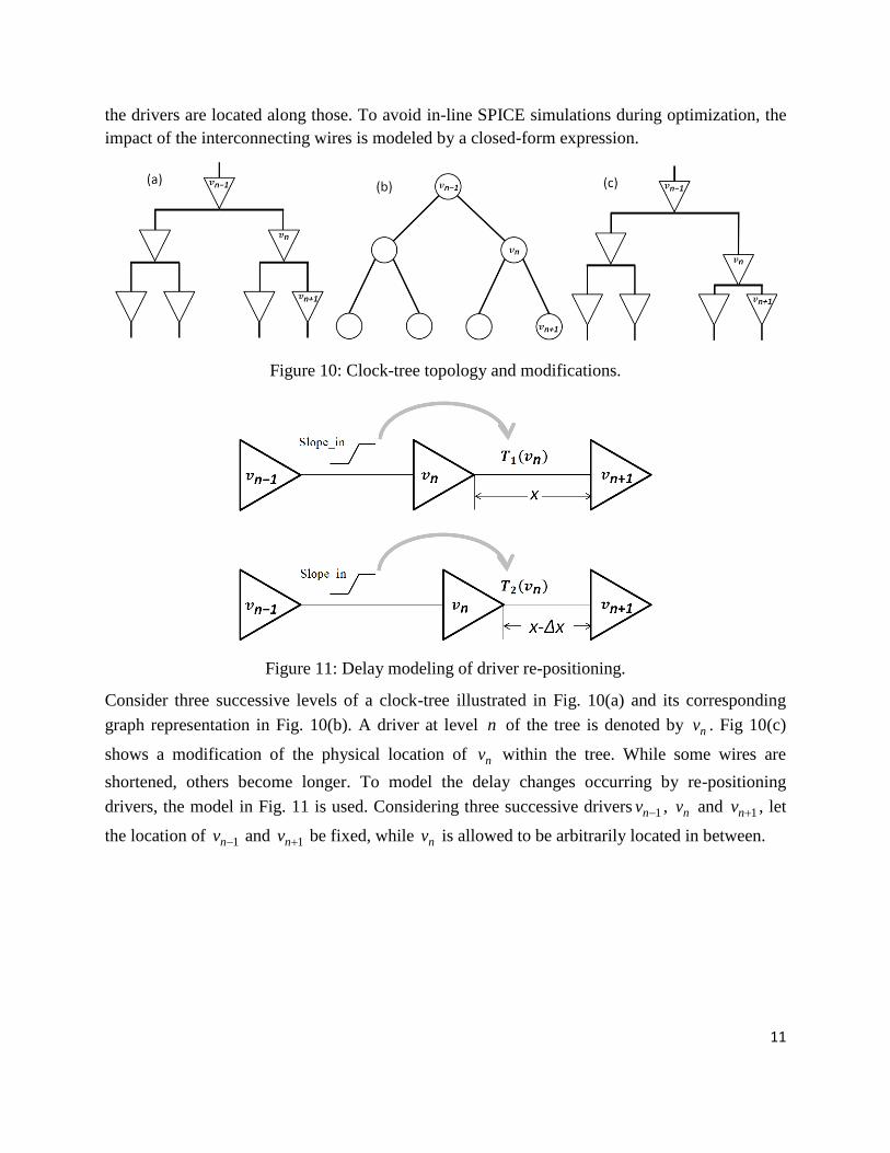
Figure 10: Clock-tree topology and modifications.
Figure 11: Delay modeling of driver re-positioning.
Consider three successive levels of a clock-tree illustrated in Fig. 10(a) and its corresponding
graph representation in Fig. 10(b). A driver at level n of the tree is denoted by nv . Fig 10(c)
shows a modification of the physical location of nv within the tree. While some wires are
shortened, others become longer. To model the delay changes occurring by re-positioning
drivers, the model in Fig. 11 is used. Considering three successive drivers 1nv , nv and 1nv , let
the location of 1nv and 1nv be fixed, while nv is allowed to be arbitrarily located in between.

12
Figure 12: The delay dependency on driver position.
The resulting delay obtained by SPICE is shown in Fig. 12. It linearly depends on the location of
nv . Four clock-drivers, two LVT and two HVT, of different strength were simulated. Linear
behavior is shown across wide range of wire lengths and clock-driver types. The linear behavior
adheres the following equation
delay 1 2 delayn nT v T v K x , (3)
where x is wire length change in microns and delayK is a factor measured in picoseconds per
micron, obtained by SPICE simulations. By using (3) to account for the delay changes occurring
by displacing drivers, the clock-tree construction and optimization algorithm avoids the
expensive simulations. It is important to note that delayK is another characteristics data of a
driver. Similarly, the output slope outS of nv is changed due to repositioning nv , and a similar
relation exists as follows
slope 1 2 slopen nS v S v K x . (4)
The parameter slopeK is another characteristic data of a driver, obtained by SPICE simulation
shown in Fig. 13 to linearly depend on the location of nv .
13
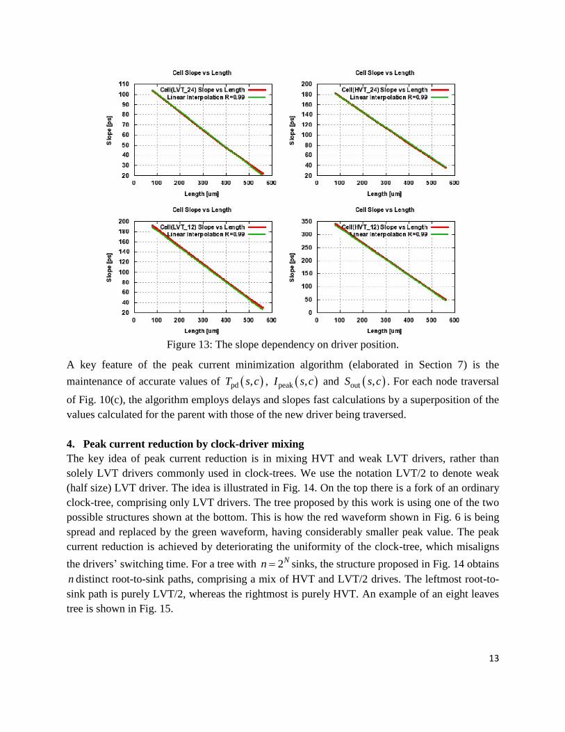
Figure 13: The slope dependency on driver position.
A key feature of the peak current minimization algorithm (elaborated in Section 7) is the
maintenance of accurate values of pd ,T s c , peak ,I s c and out ,S s c . For each node traversal
of Fig. 10(c), the algorithm employs delays and slopes fast calculations by a superposition of the
values calculated for the parent with those of the new driver being traversed.
4. Peak current reduction by clock-driver mixing
The key idea of peak current reduction is in mixing HVT and weak LVT drivers, rather than
solely LVT drivers commonly used in clock-trees. We use the notation LVT/2 to denote weak
(half size) LVT driver. The idea is illustrated in Fig. 14. On the top there is a fork of an ordinary
clock-tree, comprising only LVT drivers. The tree proposed by this work is using one of the two
possible structures shown at the bottom. This is how the red waveform shown in Fig. 6 is being
spread and replaced by the green waveform, having considerably smaller peak value. The peak
current reduction is achieved by deteriorating the uniformity of the clock-tree, which misaligns
the drivers’ switching time. For a tree with 2Nn sinks, the structure proposed in Fig. 14 obtains
n distinct root-to-sink paths, comprising a mix of HVT and LVT/2 drives. The leftmost root-to-
sink path is purely LVT/2, whereas the rightmost is purely HVT. An example of an eight leaves
tree is shown in Fig. 15.

14
Figure 14: Mixing LVT and HVT clock-drivers in clock-tree.
Figure 15: 3-level clock-tree mixing HVT and LVT/2 drivers.
Let ,T V E be the clock-tree (see Fig. 10(b)), which nodes V are the clock drives. The terms
nodes and drivers are used interchangeably. The edges E are the wires connecting parents to
sons. The set Q V denotes T ’s leaves, where the FFs are connected. T is assumed to be a
binary balanced tree (see Fig. 5). This is a common assumption in the development of
algorithms, which does not limit the generality of the discussion. Each node v V is associated
with the following parameters, accumulated along the tree traversal, using the characteristic data
of driver types, shown in Fig. 8.
1. c v : capacitive load driven by v .
2. pd ,T u v : propagation delay from the output of the parent u to the output of its son v .
3. pd_totT v : propagation delay from T ’s root to the output of v .
4. s v : voltage slope at v ’s output.

15
While the peak current is reduced, the clock skew at the sinks, defined by the difference between
the maximum and minimum root-to-sink latency, should be maintained within a prescribed limit.
This could be achieved if the propagation delays from the root of the two branches in Fig. 14 to
their far end will stay equal, thus avoiding skew accumulation. Fig. 16 shows the propagation
delays of the two branches obtained by SPICE simulation. The magnified crossing point of the
two voltage responses shows that the 50% to 50% delay difference between the two branches is
3.6 picoseconds, which is less than 0.5% of 1GHz clock frequency. Similar behavior was
observed for all the clock-drivers in 40 manometers technology. Another important advantage is
the leakage current reduction due to the HVT and weaker LVT/2 drivers.
Figure 16: Propagation delays equalities of HVT and LVT/2 branches.
The simulation in Fig. 16 used equal loads at the far ends of the two branches. This however is
not sufficient to guarantee that the root-to-leaf delays of the entire tree will stay within
acceptable skew. The peak current reduction algorithm by its very nature displaces the location
of drivers in its top-down phase. This in turn changes the loads seen by the branches, and their
propagation delays are therefore not equal any more. To this end a bottom-up phase maintains
the global skew within a prescribed limit by further driver displacement. Though local delay
inequalities at branches occur, those do not matter, as after all what counts is the global root-to-
leaf delays and if those are made equal, the goal of small skew is achieved.
We shall use the property of delay linearity shown in (3) and Fig. 12 to obtain zero local skew at
the top-down traversal phase. Though not guaranteeing global zero skew (root-to-leaf), it is a
first step towards skew convergence. Skew corrections are performed by a bottom-up traversal,
where a fine tuning of the drivers’ location (wire stretching) fixes the skew occurred due to the
blindness of the top-down traversal to the global delay.
16
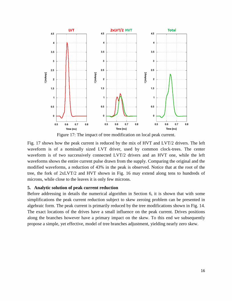
Figure 17: The impact of tree modification on local peak current.
Fig. 17 shows how the peak current is reduced by the mix of HVT and LVT/2 drivers. The left
waveform is of a nominally sized LVT driver, used by common clock-trees. The center
waveform is of two successively connected LVT/2 drivers and an HVT one, while the left
waveforms shows the entire current pulse drawn from the supply. Comparing the original and the
modified waveforms, a reduction of 43% in the peak is observed. Notice that at the root of the
tree, the fork of 2xLVT/2 and HVT shown in Fig. 16 may extend along tens to hundreds of
microns, while close to the leaves it is only few microns.
5. Analytic solution of peak current reduction
Before addressing in details the numerical algorithm in Section 6, it is shown that with some
simplifications the peak current reduction subject to skew zeroing problem can be presented in
algebraic form. The peak current is primarily reduced by the tree modifications shown in Fig. 14.
The exact locations of the drives have a small influence on the peak current. Drives positions
along the branches however have a primary impact on the skew. To this end we subsequently
propose a simple, yet effective, model of tree branches adjustment, yielding nearly zero skew.

17
Figure 18: Delay model of a clock-driver fork.
Consider the RC-delay model of the fork illustrated in Fig. 18(a), where the root is either HVT or
LVT/2 driver, with internal resistance trR . The model comprises two types of driver-to-driver
interconnects. Fig. 18(b) models the delay from the root driver to the HVT driver and the first
LVT/2 one, while Fig. 18(c) models the delay from the first LVT/2 driver to the second one.
g(H)C and g(L/2)C denote the input gate capacitance of HVT and LVT/2 delivers, respectively.
We use the notation int( ) int HHR r x and int( ) int HHC c x for resistance and capacitance,
respectively, of the wire connecting the root to the HVT driver. intr and intc are per-micron
resistance and capacitance coefficients, respectively, and Hx is a wire length variable. Similar
conventions are used for LVT/2 wire connection.
Using Elmore delay model [25 Ch. 5], the delay H from the root to the HVT driver is
int HH tr int L/2 g(L/2) tr int H tr int H g(L/2)
2int intH tr int H L/2 int g(H) tr int H tr g(H) g(L/2)
2
( )2
r xR c x C R c x R r x C
r cx R c x x r C R c x R C C
. (5)
The delay L/2 from the root to the first LVT/2 gate is the following
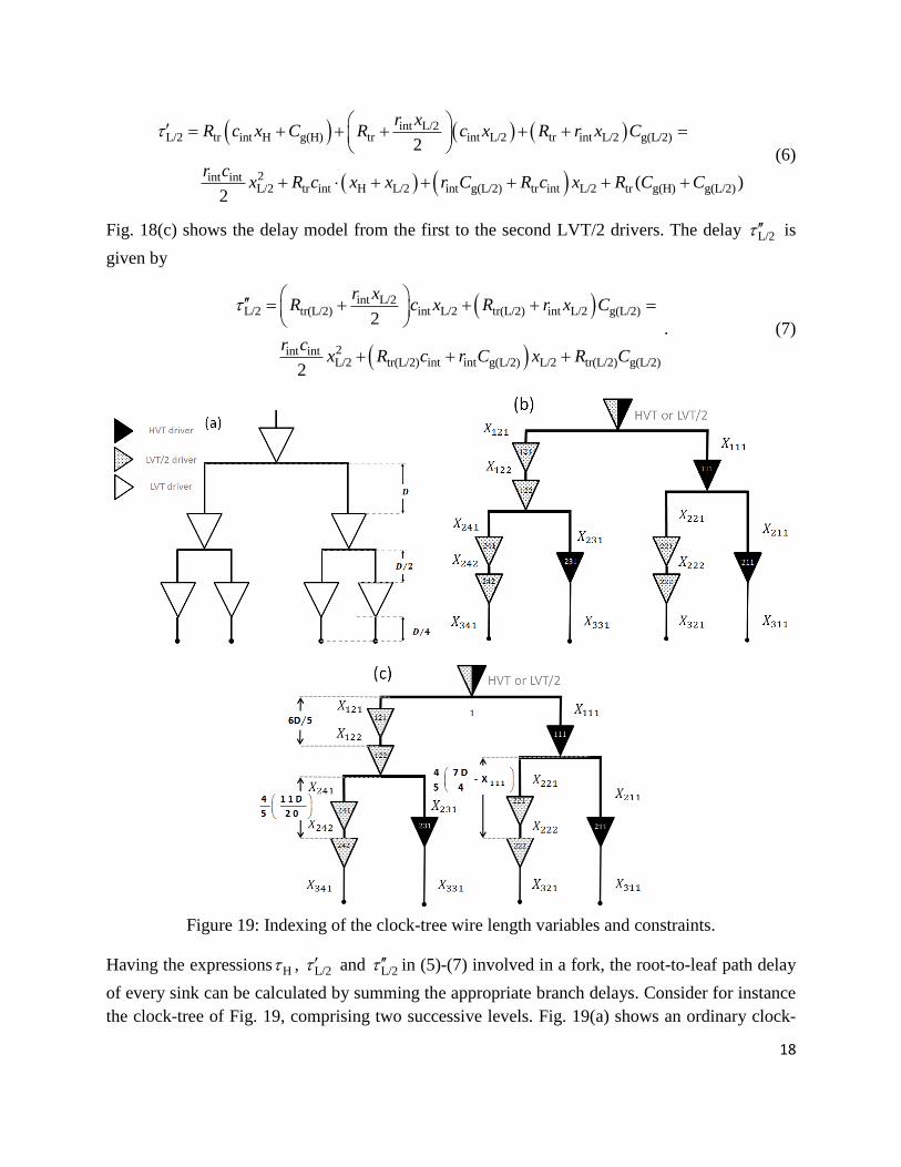
18
int L/2L/2 tr int H g(H) tr int L/2 tr int L/2 g(L/2)
2int intL/2 tr int H L/2 int g(L/2) tr int L/2 tr g(H) g(L/2)
2
( )2
r xR c x C R c x R r x C
r cx R c x x r C R c x R C C
(6)
Fig. 18(c) shows the delay model from the first to the second LVT/2 drivers. The delay L/2 is
given by
int L/2L/2 tr(L/2) int L/2 tr(L/2) int L/2 g(L/2)
2int intL/2 tr(L/2) int int g(L/2) L/2 tr(L/2) g(L/2)
2
2
r xR c x R r x C
r cx R c r C x R C
. (7)
Figure 19: Indexing of the clock-tree wire length variables and constraints.
Having the expressions H , L/2 and L/2 in (5)-(7) involved in a fork, the root-to-leaf path delay
of every sink can be calculated by summing the appropriate branch delays. Consider for instance
the clock-tree of Fig. 19, comprising two successive levels. Fig. 19(a) shows an ordinary clock-

19
tree with a fork length parameter D , and a level-to-level length reduction by factor two (see the
H-tree in Fig. 5). Fig. 19(b) is the modified tree, where wire lengths variables ***x are
introduced to tune the root-to-leaf delays for skew nullifying. The solution (not necessarily
unique) finds appropriate locations of drivers along their branches. Driver-to-driver interconnects
lengths are variables, where their partial sums must satisfy branch lengths constraints, dictated
by the methodology of level-to-level wire length reduction by factor two.
Let the clock-tree have n leaves. To keep track of the wire-length variables, we adopt the triplet
indexing notation , ,m k l of the drivers, where, 21 logm n is the tree level, 1 2mk is the
driver’s index within the level, and 1,2l is an index, used to distinguish between the two
cascaded LVT/2 drivers along their branch (see Fig. 18(b)). For the sake of uniformity an HVT
driver is always indexed by 1. Driver’s incoming wires inherit the driver’s , ,m k l index. In the
above convention the wires connected to the output of the leaf drivers in Fig 19(b) are assumed at
level 3.
To zero the skew, all the root-to-leaf latencies must be the same, say latencyT (another degree of
freedom). One can derive from (5)-(7) n root-to-leaf equations, whose matrix notation is
2latency 1 0X X C T A B . (8)
X in (8) is the vector of wire-length variables, whose length is 4 3n , A and B are matrices of
size 4 3n n and C is a vector of length n . Their entries are derived from (5)-(7).
The solution of (8) must satisfy the geometric constrained imposed by the pre-defined tree
length, dictated in Fig. 19(a). Those constraints are of two types. The first type comprises n
constraints accounting for the tree’s total length, given by 2log
02 2 1
n i
mD D n n
. The
second type constraints are aimed at maintaining the relative length of the forks according to
their level. Recalling that a fork length is inherited from its parent fork by the factor half, it is
only the first driver in the LVT/2 branch that has the freedom to be displaced within the fork, as
shown in Fig. 19(c). That yields other 1n constraints. All in all there are 2 1n wire length
constraints, presented by
X LF , (9)
where F is a 2 1 4 3n n matrix and L is the constraints vector of length 2 1n . If the
system of n quadratic equations in (8) and 2 1n linear equations in (9), of the 4 2n variables
( latencyT is a variable too) has a real solution, zero skew is achieved.
6. Algorithm for clock-tree construction

20
We subsequently present an algorithm to reduce the peak current and maintain minimum skew,
by the tree modifications proposed in Fig. 14 and wire lengths adjustments illustrated in Section
5. The algorithm comprises two phases. The first is a top-down traversal. Its primary goal is to
cut the peak supply current. It also maintains small skew in an ad-hoc manner, ensuring it does
not escape at the tree’s leaves. That is a good starting point to a second phase of bottom-up
traversal, aiming at skew nullifying by fine adjustments of the clock-drivers positions in the tree
branches. The second phase has a very small impact on the peak current, which has already been
reduced in the first phase.
Starting at the root, for each visited node, the top-down traversal does the following:
1. Substitution of a fork mixing HVT and LVT/2 drivers as illustrated in Fig. 14.
2. For both the HVT and LVT/2 fork’s branches, the cumulative delay from the root, and the
slope at the branch driver’s output are calculated.
3. The position of the HVT driver is adjusted to ensure equal delay from the root to the far end
HVT and LVT/2 drivers. Delay equalization is done by numerical, binary search iterations,
using the driver’s characteristics presented in Section 3.
Starting at the leaves, for each visited node, the bottom-up traversal does the following:
1. It calculates the delay deviations which have been resulted at the top-down phase. This
deviation occurs due to the blindness of the top-down calculations to the loads of the drivers
in the HVT and LVT/2 branches, as such loads are affected by the position adjustments of
the HVT driver that has not been decided yet.
2. Nullifying the skew at the node, by fine adjustments of the locations of the LVT/2 and the
HVT drivers.
6.1 Current waveform construction
Once the bottom-up traversal completes, the entire clock-tree is determined. The current
waveform at the tree’s root can be accurately computed by cumulating the currents drawn by the
individual drivers. The skew supposed to be small, though not yet meeting the prescribed limit.
21
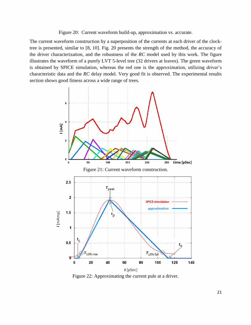
Figure 20: Current waveform build-up, approximation vs. accurate.
The current waveform construction by a superposition of the currents at each driver of the clock-
tree is presented, similar to [8, 10]. Fig. 20 presents the strength of the method, the accuracy of
the driver characterization, and the robustness of the RC model used by this work. The figure
illustrates the waveform of a purely LVT 5-level tree (32 drivers at leaves). The green waveform
is obtained by SPICE simulation, whereas the red one is the approximation, utilizing driver’s
characteristic data and the RC delay model. Very good fit is observed. The experimental results
section shows good fitness across a wide range of trees.
Figure 21: Current waveform construction.
Figure 22: Approximating the current pule at a driver.

22
Fig. 21 shows how a current waveform is constructed for the modified tree of 8 sinks (leaves).
Such a tree has a total of 8 1 3 21 HVT and LVT/2 divers. The current drawn at each
drivers and its relative time alignment is progressively computed from top-to-bottom. The slope
and capacitive loads at each node are calculated, and with the aid of the ,s c slope-load driver
characteristics (see Section 3, Figs. 5(a)-(c)), the currents and their relative time alignments are
derived. Based on peakI , peakT , 10% riseT and 10% fallT defined in Section 3, a triangular
approximating the driver’s current waveform is defined. That triangle is defined by three time
parameters st , pt and et , shown in Fig. 22. Notice their relation to peakT , 10% riseT and 10% fallT in
Fig. 9.
7. Algorithm details
We subsequently describe in details steps algorithm, with emphasis on the computational
aspects. The top-down peak current reduction is described first, followed by the bottom-up
drivers’ position adjustment for skew nullifying.
7.1 Top-down peak current reduction
The primary goal of the top-down phase is to reduce the peak current. It also maintains the skew
within reasonably small value, which can afterwards be nullified by further tuning. Fig. 23
illustrates the fork substitution with respect to an ordinary clock-tree, where the various points
are numbered for reference. We denote by ,i jl the length between two points i and j , and by
,i j the 50% to 50% propagation delay along a wire connecting i with j . H and L/2 denote
the intrinsic delay of HVT and LVT/2 clock-drivers, respectively. Recall that H and L/2 are
functions of their output load and input slope, and can be obtained by a two-dimensional linear
interpolation of the characteristic data described in Section 3.
Figure 23: Wire length budgeting in fork substitution.

23
Fig. 23(a) shows the relations between the lengths of an ordinary tree’s branches, adhering the
level-to-level length reduction by factor two (see the H-tree in Fig. 5). There is
1
2
nn
DD , (10)
where n denotes the level of the tree (see Fig. 10). The substituted tree in Fig. 19(b) maintains
wire length invariance by imposing the following 3 2D total length on two successive tree levels
3 3 3 3
5 5 10 2
D D D D , and
3 3
2 2
D Dx x
,
where x is a variable set at the top-down phase to ensure delay equality of the two fork’s
branches. There is some blindness of the far end capacitive loads since fork substitution in the
successive level of the tree will change the length of the far end wires. The temporary top-down
delay equalization ensures the global skew measured at the tree’s leaves is not escaping, such
that the bottom-up wire lengths fine tuning can recover the skew to be nearly zero.
Referring to the numbers in Fig. 23(b), the delay equalization is obtained by the substitution
1,2 H(2,3) 1,6 2(6,7) 7,8 2(8,9)L L . (11)
Notice that the drivers’ intrinsic delays H(2,3) , 2(6,7)L and 2(8,9)L in (11) are associated with the
position in the tree’s branch, since those delays depend on their input slope and output capacitive load,
varying along the branch. For the wire delays of (11) there is
2
int int1,6 7,8 int g
3 3 = =
5 2 5
r cD Dr C
, (12)
2 int int1,2 int g =
2
r cx xr C , (13)
where intr is the wire’s resistance per micron and intc is its capacitance per micron, both taken
from TSMC for 40 nanometer technology. gC is the gate capacitance of the TSMC drivers which
has been used for this study. For (12) and (13) we used the interconnect delay model in [25, Ch.
5].
The intrinsic delays of the drivers are obtained from the characteristic data. Shown in Fig. 8,
those are discrete functions of the input slope and the output load. To find H(2,3) , 2(6,7)L and
2(8,9)L in (11) , the slope at point 1 in Fig. 23 is known from the p fork calculation, and the wire
loads 1-2 and 1-6 can be calculated from intr , intc and gC . Those are used to propagte the slope
from point 1 to 2 and to 6. The laods driven by the drivers at points 2 and 6, comprising the wires
and gate capacitance of the drivers connected at their far ends, can also be calculated. Shown in

24
Fig. 24, by knowing the input slopes inS and the output loads loadC , a two dimensional
interpolation finds the intrinsec delays of the drivers connected at points 2 and 6.
Figure 24: Two-dimensional driver’s intrinsic delay interpolation.
By using four adjacent grid points of Fig. 24, indexed (1,1), (1,2), (2,1) and (2,2), the following
expression interpolates the propagation delay pdT at points 3 and 7 in Fig. 23.
1,1 2,1 1,2 2,1 1,1 2,2pd in in load load pd in in load load
1,2 2,1 1,1 2,2 1,1 1,1pd in in load load pd in in load load
pd in load 2,1 1,1 2,2 1,1in in load load
- - - -
- - - -, .
- -
T S S C C T S S C C
T S S C C T S S C CT S C
S S C C
(14)
Similarly, a two-dimentional interpolation for the slopes outS at points 3 and 7 in Fig. 23 is
1,1 2,1 1,2 2,1 1,1 2,2out in in load load out in in load load
1,2 2,1 1,1 2,2 1,1 1,1out in in load load out in in load load
out in load 2,1 1,1 2,2 1,1in in load load
- - - -
- - - -, .
- -
S S S C C S S S C C
S S S C C S S S C CS S C
S S C C
(15)
To complete the fork calculations, it is required to further propagate the delay and slope from
point 7 to 8, and then from 8 to 9. Those are obtained by similar techniques and equations (12)-
(15).
Fig. 23(b) shows that the fork calculations depend on x , which supposed to solve (11). The
solution can be obtained by any search method, where iterations require re-calculation of the
fork’s right branch delays, using drivers’ characteristics for computational efficiency’ avoiding
run-time explosion if SPICE simulation have been used. We used binary search to solve (11).
Fork substitution takes place at each tree’s node. Once done, substitution of its left and right sons
takes place. We subsequently detail the calculations of the left fork at point 9, shown in Fig. 25.

25
The first step is to define the fork’s total length budget. For point 1 that was 2 3 2D D D . For
the left fork at point 9 that would be 3 10 4 11 20D D D . This is shown by the distance
between points 9 and 11, supposed to consume 2 5 of that budged, yielding
altogether 2 5 11 20D .
In the right branch the length z between points 9 and 10 (denoted by x in the parent) is sought
such that delays equality as in (11) is solved for the fork emanating at point 9. By similar
considerations, the length budget of the right son fork is 3 2 4 7 4D x D D x . Then the
branch length y between points 3 and 4 is sought to solve (11).
Figure 25: Wire length solution to ensure delay equalities at sibling son drivers.
To solve (11) for the entire tree, a top-down tree traversal can be implemented by a recursive call to an
appropriate software function. There is a delicate point though. The solution of (11) for a given fork
(tree’s node) is blind to the later solution that will take place in its son forks, while the capacitive loads
assume the default positions setting in Fig. 23(b). Those are adjusted by subsequent invocations of the
recurrence, so the delays and slopes calculated at points 3 and 9 in Fig. 23(b) are inaccurate. The slope is
corrected simultaneously with the son fork solution by applying the linearization in (4). For practical
reasons and computational efficiency, the delay correction in (3) takes place at the bottom-up phase, as it
anyway re-adjusts the length connecting point 7 to 8 for global skew zeroing, as subsequently described.
7.2 Bottom-up delay correction
The blindness of the top-down fork substitutions to the downstream loads resulted delay
inaccuracies. This in turn may lead to non-negligible clock skew at the tree’s leaves. While the
slopes ate points 3 and 9 have already been precisely computed at the top-down traversal, it is the
role of the bottom-up phase to resolve delay discrepancies to yield nearly zero skew. To this end,
position adjustments of the LVT/2 driver residing between points 6 and 7 in Fig. 25 takes place.
The wire length between points 1 and 9, dictated by the top-down traversal, remains unchanged.

26
When the bottom-up phase is invoked, the lengths x , y and z shown in Fig. 25, are already
determined for the entire tree.
Comparing Fig. 25 to 23(b), the delay discrepancy at point 3 occurs due to the difference
between the length 3 2D x which has been used for the top-down delay calculation from point
3 to points 4 and 5, while the substitution of the son fork changed those to y and to
2 5 7 4D x , respectively. The accurate delay at 3 can be found from equation (3) by
accounting for the differences 3 2y D x and 2 5 7 4 3 2D x D x at the right
branch left branches, respectively. The delay correction at point 3 is therefore
delay H(2,3) delay H(2,3)
2 7 32
5 4 2
D DK y x x
. (16)
The delay correction at point 9 is
delay 6,9 delay 6,9( ) ( ) 11 50 2 3 10K z D D , (17)
where 6,9 is a compound linearization factor between points 6 and 9.
Fig. 26(a) illustrates a fork and its left and right emanating sub-trees. The equality of all the
latencies in a sub-tree is the invariant of the bottom-up latency equalization process. Fig. 26(b)
exemplifies the three lowermost levels of a sub-tree, where pd1 pd2 pd3, , T T T and pd4T are the root-
to-leaf latencies. Notice that each of the four lowest forks at points 4, 5, 6 and 7 satisfies the
invariant property of left and right branch delay equalities by the to-down construction. That
happens since the loads at the leaves are the FFs clock input loads, which are accurately known.
The operation taken at point 2 in Fig. 26(b) aims at equating pd1T with pd2T , and similarly at point
3 for pd3T with pd4T , yielding the situation shown in Fig. 26(a).

27
Figure 26: Invariants of the bottom-up latency equalization.
The evaluation of (16) and (17) ensures that the latencies pdT and pdT , shown in Fig. 26(a), are
accurately known (though not equal yet). Once pdT with pdT are equalized, they will stay so
regardless of any further bottom-up manipulation at higher levels. We subsequently describe
how pd pdT T is nullified. In terms of Fig. 26 the solution of
1,2 H(2,3) 1,6 2(6,7) 7,8 2(8,9) pd delay H(2,3) pd delay 6,9( ) ( )L L T T
(18)
is in order. Equation (18) is numerically solved by a binary search of the position of the LVT/2
driver connected between points 6 and 7 in Fig. 25, where the wire length between points 1 and 8
is not changed. The solution of (18) also uses driver characteristics. Another delicate point to
consider is that the solution of (18) changes the load seen at point 1 in Fig. 25, which in turn
changes the slope at the point. Those variations are accounted and maintained in the numerical
solution with the aid of the linearization in (4).
7.3 Putting everything together in a code
Sections 7.1 and 7.2 described the top-down and bottom-up numerical node solution,
respectively. Though those involve different computations, they can be captured in a single
recursive traversal procedure. As the recursion dives (top-down) into a node, the fork
substitution of Section 7.1 takes place. As the recursion returns from a sub-tree to its root node
(bottom-up), the left and right delay equalization of Section 7.2 takes place. An appropriate
pseudo code is shown in Fig. 27. It is called for every node v where a fork is substituted, passing
the following parameters:
1. s v : input slope of v ,

28
2. pd_totT v : latency from tree’s root to v ,
3. LenBudjet: fork length budget substituted at v , passed from the parent node, and
4. D : additional budget of the fork length.
Each node of the tree (driver’s output), maintains an internal data structure, storing slope and
root-to-node latency, length of the left and right outgoing wires, delay and slope linearization
factors used in (3) and (4), respectively, and driver’s type. The code below refers to the notations
of Fig. 23 and Fig. 25.
DelayType: NodeTraverse( s v , pd_totT v , LenBudjet , D ) {
LenBudjet LenBudjet D ; // update fork’s wire length budget
( rightx , rights v , lefts v , pd_tot rightT v , pd_tot leftT v , delayK , slopeK ) =
ForkCalc( s v , pd_totT v , LenBudjet ); // apply fork delay and slope calculations
NodeUpdate ( rightx , leftx , pd_totT v , “top-down”);
SonUpdate( rights v , rightx , pd_tot rightT v ); // right son lengths, delay and slopes updates
SonUpdate( lefts v , leftx , pd_tot leftT v ); // left son lengths, delay and slopes updates
// traverse right sub-tree
delay H(2,3)
NodeTraverse( rights v , pd_tot rightT v , rightLenBudjet x , 2D );
// traverse left sub-tree
delay 6,9
NodeTraverse ( lefts v , pd_tot leftT v , 1 5 LenBudjet , 2D );
// fixes delay discrepancy by finding the appropriate location of LVT/2 driver
if ( delay H(2,3) 0 or delay 6,9 0 ) {
( leftx , delay ) = DelayCorrection( s v , pd_totT v , rightx , LenBudjet );
// updates lengths, delay and slopes of node
NodeUpdate( leftx , LenBudjet , pd_totT v , “bottom-up”);
return ( delay );
}
else { return 0; }
} // NodeTraverse
Figure 27: Pseudo code of recursive node traversal.

29
The recursive function NodeTraverse is being called for the root of the clock-tree. Upon
completion, the accurate root-to-node delay, slope and wire capacitive loads, are known for each
node. Those, together with the aid of the characteristic data, enable the buildup of the current
waveform by the triangle superposition described in Section 6.1.
8. Experimental results
Several clock-trees have been implemented, using the fork substitution algorithm. For each of
those trees the current pulse waveform, the skew, and the sensitivity of the skew to input slope,
have been measured in two manners. First, the computational engine of the algorithm together
with the driver characteristics, have been used. The resulting tree was then simulated with
SPICE. Very good correlation between the two across a wide range of clock-trees is shown.
8.1 Peak current reduction and computation accuracy
Fig. 28 shows from left to right the peak current achieved by the fork substitution algorithm for
3-level, 4-level and 5-level clock-trees, comprising 8, 16 and 32 sinks, respectively (green
waveforms), compared to the ordinary clock-tree (red waveforms). Both the ordinary and
modified trees have been simulated in SPICE.
Figure 28: Peak current reduction of clock-trees obtained by fork substitution algorithm.
Notice the clear local peaks in the ordinary tree, aligned in time according to the tree levels,
where the highest peak occurs at the leaves, comprising half of the total drivers count. It can be
observed that 30% to 45% peak current reduction was achieved. While the global clock network
may be a mesh or spine, clock-trees are widely used for the local clock distribution [9]. Since
such trees are more or less uniformly distributed across the entire silicon area, it ensures the
effectiveness of the power noise reduction. Expectedly, the latency of the modified waveform is

30
longer than the original one in a reciprocal proportion of the peak current reduction, since the
area under the waveform (charge) should be about the same.
Figure 29: Accuracy of fork substitution algorithm compare to SPICE.
8.2 Model accuracy
To validate its accuracy, the current waveforms obtained by the fork substitution algorithm (red
waveforms) were compared to those obtained by SPICE simulation (green waveforms). Good
fitness is shown in Fig. 29, where accuracies of 10% for 3-level and 4-level trees and 3% for 5-
level tree were measured.
8.3 Small skew validation and slope variations
To validate that nearly zero skew has been achieved, the response of a clock pulse was measured
at the leaves by SPICE simulations, showm in Fig. 30. The 50% ddV crossings are encircled. It is
clearly seen that all responses are crossing 50% ddV almost simultaneously, showing that the
small skew premise is achieved.

31
Figure 30: Zero skew validation.
Figure 31: Skew sensitivity to slope of clock signal at tree’s root.
Another important aspect of the skew is its sensitivity to the slope of the clock signal driving the
root of the tree. To this end the signal with slopes varying from 28pSec to 64pSec were
simulated with SPICE. The results showm in Fig. 31, indicate that for a wide range of input
slopes, the skew is maintained in the range of 1pSec to 8pSec. For clock cycle of 1GHz this is
less than 1% of the clock cycle in the worst case. Furthermore, Fig. 31 shows well behaviour of
the algorithm with respect to the tree size, maely the skew behaves similarly for the three trees.
References:

32
1. Popovich, Mikhail, Andrey V. Mezhiba, and Eby G. Friedman. Power distribution
networks with on-chip decoupling capacitors. Vol. 13. Springer, 2008.
2. R. Joseph, D. Brooks, and M. Martonosi, “Control techniques to eliminate voltage
emergencies in high performance processors,” in Int’l Symposium on High-Performance
Computer Architecture, 2003.
3. Gupta MS, Oatley JL, Joseph R, Wei G-Y, Brooks DM(2007) “Understanding voltage
variations in chip multiprocessors using a distributed power-delivery network,” Design,
Automation & Test in Europe Conference & Exhibition, April 2007, pp1-6.
4. L.D. Smith, R. E, Anderson and T. Roy “Chip-Package Resonance in Core Power Supply
Structures for a High Power Microprocessor” Proceedings of the ASME International
Electronic Packaging Technical Conference and Exhibition, July 2001.
5. H.E. Neil and H.M. David, “Integreated Circiut Design” (Forth Ed), Pearson, Chapter
12.3, pp. 513-524.
6. Salman E. and Friedman E. G., High Performance Integrated Circuit Design, McGraw-
Hill, 2012, Chapter 10.
7. W. Laung-Terng, C. Yao-Wen and C. (Tim) Kwang-Ting, “Electronic Design
Automation: Synthesis, Verification, and Test (Systems on Silicon),” Morgan-
Kaufmann, 2009, Chapter 13, pp. 751-760.
8. Kim, Yooseong, Sangwoo Han, and Juho Kim. “Power supply noise reduction by clock
scheduling with gate-level current waveform estimation.” SoC Design Conference, 2008.
ISOCC’08. International. Vol. 2. IEEE, 2008.
9. Tam S. (Xanthopoulos T., Ed.), Clocking in Modern VLSI Systems, Chapter 2, Springer,
2009.
10. P. Vuillod, L. Benini, A. Bogliolo, and G. De Micheli. Clock skew optimization for peak
current reduction. In Proc. Int’l Symp. on Low Power Electronics and Design, pages
265–270,Aug. 1996.
11. Fishburn, John P. “Clock skew optimization.” Computers, IEEE Transactions on 39.7
(1990): 945-951.
12. Lam, W-CD, Cheng-Kok Koh, and Chung-Wen Albert Tsao. “Clock scheduling for
power supply noise suppression using genetic algorithm with selective gene
therapy.” Quality Electronic Design, 2003. Proceedings. Fourth International
Symposium on. IEEE, 2003.
13. Yu, Zhentao, Marios C. Papaefthymiou, and Xun Liu. “Skew spreading for peak current
reduction.” Proceedings of the 17th ACM Great Lakes symposium on VLSI. ACM, 2007.
14. Tschanz J. (Xanthopoulos T., Ed.), Clocking and Variations, Chapter 7, Springer, 2009.

33
15. Nieh, Yow-Tyng, Shih-Hsu Huang, and Sheng-Yu Hsu. “Minimizing peak current via
opposite-phase clock tree.” Proceedings of the 42nd annual Design Automation
Conference. ACM, 2005.
16. Joo, Deokjin, and Taewhan Kim. “A Fine-Grained Clock Buffer Polarity Assignment for
High-Speed and Low-Power Digital Systems.” IEEE TRANSACTIONS ON COMPUTER-
AIDED DESIGN OF INTEGRATED CIRCUITS AND SYSTEMS 33, no. 3 (2014): 423-
436.
17. R. Samanta, G. Venkataraman, and J. Hu, “Clock buffer polarity assignment for power
noise reduction,” in Proc. IEEE/ACM Int. Conf. Comput.-Aided Design, 2006, pp. 558–
562.
18. P.-Y. Chen, K.-H. Ho, and T. Hwang, “Skew-aware polarity assignment in clock tree,”
ACM Trans. Des. Autom. Electron. Syst., vol. 14, no. 2, pp. 31:1–31:17, Mar. 2009.
19. Y. Ryu and T. Kim, “Clock buffer polarity assignment combined with clock tree
generation for power/ground noise minimization,” in Proc. IEEE/ACM Int. Conf.
Comput.-Aided Design, 2008, pp. 416–419.
20. M. Kang and T. Kim, “Clock buffer polarity assignment considering the effect of delay
variations,” in Proc. IEEE Int. Symp. Quality Electron. Design, 2010, pp. 69–74.
21. J. Lu and B. Taskin, “Clock buffer polarity assignment considering capacitive load,” in
Proc. IEEE Int. Symp. Quality Electron. Des., 2010, pp. 765–770.
22. Jang, Hochang, Deokjin Joo, and Taewhan Kim. “Buffer sizing and polarity assignment
in clock tree synthesis for power/ground noise minimization,” Computer-Aided Design of
Integrated Circuits and Systems, IEEE Transactions on 30.1 (2011): 96-109.
23. M. Sarrafzadeh and C. K. Wong “An Introduction to VLSI Physical Design”, McGraw-
Hill, 1996, Chapter 4.3.3.
24. S. Gary et al., “PowerPC 603, a microprocessor for portable computers,” IEEE Design &
Test of Computers, vol. 11, pp. 14–23, 1994.
25. Bakoglu, H. “Circuit, Interconnections, and Packaging for VLSI,” Addision-Wesley.
Reading, Mass (1990).