clock and synchronization - tut 12-13 - clock... · clock and synchronization tie-50206 logic...
TRANSCRIPT

Clock and Synchronization
TIE-50206 Logic Synthesis
Arto Perttula
Tampere University of Technology
Spring 2016

Acknowledgements
• Most slides were prepared by Dr. Ari Kulmala
• The content of the slides are partially courtesy of
– Ran Ginosar
• http://www.ee.technion.ac.il/courses/048878/index.html
– Pong P. Chu
• http://academic.csuohio.edu/chu_p/rtl/rtl_instr.html
– C.E. Cummings, D. Mills, Synchronous Resets? Asynchronous Resets? I am so confused! How will I ever know which to use?
• http://sunburst-design.com/papers/CummingsSNUG2002SJ_Resets.pdf
• Recommended reading:
– Understanding Metastability in FPGAs, white paper, Altera Corporation July 2009
– D. Chen, D. Singh, J. Chromczak, D. Lewis, R. Fung, D. Neto and V. Betz, ”A Comprehensive Approach to Modeling,
Characterizing and Optimizing for Metastability in FPGAs”, ACM International Symposium on Field Programmable Gate Arrays,
2010, pp. 167 - 176
– R. Ginosar, Fourteen ways to fool your synchronizer, Ninth International Symposium on Asynchronous Circuits and Systems, May
2003, pp. 89 - 96
– R. Ginosar, Metastability and Synchronizers: A Tutorial, IEEE D&T Comp, Sep/Oct 2011
– C.E. Cummings, D. Mills, S. Golson, Asynchoronous & Synchronous Reset Design Techniques – Part Deux, SNUG Boston 2003,
Rev 1.2, 38 pages
2.2.2016 Arto Perttula 2

Contents
• Recap: Why synchronous?
• Clock distribution network and skew, Multiple-clock systems
• Metastability and synchronization failure
• Synchronizer (next week)
– Enable tick
– Handshaking and derived clocks
– Reset syncnronization
2.2.2016 Arto Perttula 3

Introduction
• This lecture handles issues concerning digital systems having multiple
clocks or external inputs from the environment that directly feed the digital
circuit
• Most synchronous one-clock blocks do not have to worry about these
things
• However, when designing ”real-life” circuits, you have to be aware of these
things
• Clocking errors are extremely hard to detect. You should avoid them in first
place with thorough reasoning.
• A tricky issue: even major vendors in the business have released
application notes on clock domain crossings that fail…
2.2.2016 Arto Perttula 4

RECAP: WHY
SYNCHRONOUS
Answer: Because it works
2.2.2016 Arto Perttula 5

Timing of a Combinational
Digital System
• Steady state
– Signal has reached a stable value
– Modeled by Boolean algebra
• Transient period
– Signal may fluctuate
– No simple model
• Propagation delay: time to reach the steady state
• Hazards: the fluctuation occurring during the transient period
a) Static hazard: glitch when the signal should be stable
b) Dynamic hazard: a glitch in transition
– Caused by multiple converging paths of an output port
2.2.2016 Arto Perttula 6

2.2.2016 Arto Perttula 7
• E.g., static-hazard (sh=ab’+bc; a=c=1) b 1->0

2.2.2016 Arto Perttula 8
• E.g., dynamic hazard (a=c=1, d=0), b 1->0

Syncronous Paradigm to
Handle Hazards
• Ignore glitches in the transient period and store the data when it has stabilized
• In a sequential circuit
– Use a clock signal to sample the signal and store the stable value in a register
– Registers introduce new timing constraints: setup time and hold time
Arto Perttula 9
because D changes
too close to clock
edge
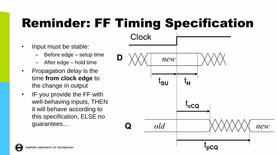
Reminder: FF Timing Specification
• Input must be stable:
– Before edge – setup time
– After edge – hold time
• Propagation delay is the
time from clock edge to
the change in output
• IF you provide the FF with
well-behaving inputs, THEN
it will behave according to
this specification, ELSE no
guarantees…

D Flip-Flop Internals
• DFF can be created from 2 D latches connected as master-
slave pair
– There are other choices as well
• First latch – master – uses inverted clock as enable
– (Perhaps internally without a separate INV)
– It’s transparent when clk=0 ans slave is latched to the old value
• Upon clk edge 0->1 slave turns transparent
• Note that rise and fall times are not 0
• If D changes near edge,
– new value may pass through the master latch
– at least partially,
– and intermediate voltage level goes to transparent slave and
– something comes out…
• This leads to DFF setup and hold constraints
Arto Perttula

Redrawn Ball Metaphor for DFF
• Outcome is obvious if D does not change near clock edge
• Outcome is obvious if ball is not dropped accurately on the middle of the hill top
12 Adapted from [Understanding Metastability in FPGAs, white paper, Altera Corporation July 2009]
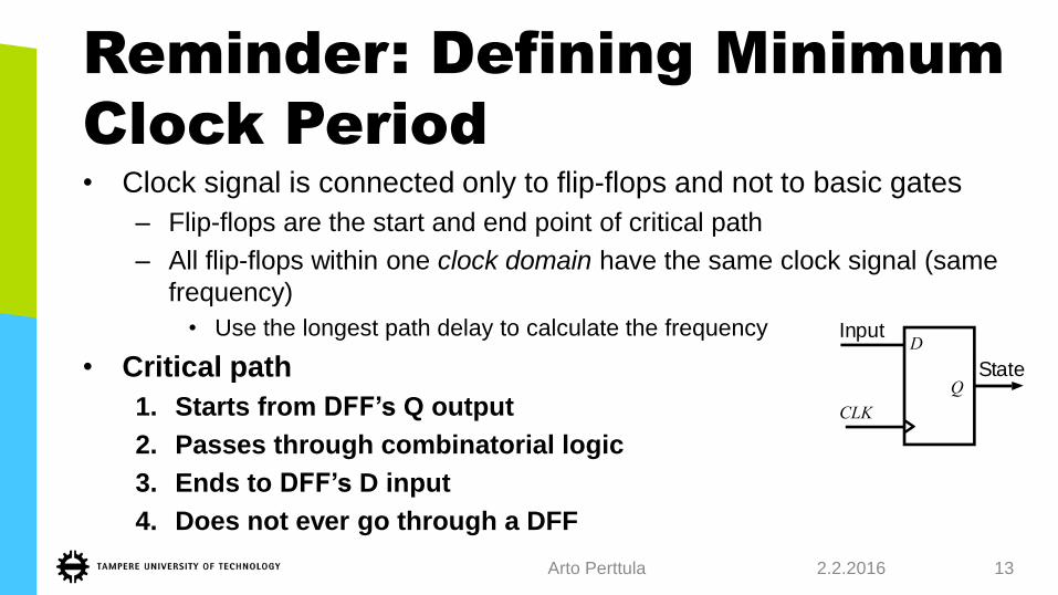
Reminder: Defining Minimum
Clock Period
• Clock signal is connected only to flip-flops and not to basic gates
– Flip-flops are the start and end point of critical path
– All flip-flops within one clock domain have the same clock signal (same
frequency)
• Use the longest path delay to calculate the frequency
• Critical path
1. Starts from DFF’s Q output
2. Passes through combinatorial logic
3. Ends to DFF’s D input
4. Does not ever go through a DFF
2.2.2016 Arto Perttula 13
CLK
Q
DInput
State

Reminder: Defining Minimum
Clock Period
• Clock signal is connected only to flip-flops and not to basic gates
– Flip-flops are the start and end point of critical path
– All flip-flops withing one clock domain have the same clock signal (same
frequency)
• Ensure that tclk_priod ≥ tcrit.path
– Analyze all paths QD and use the longest path delay to calculate the frequency
• Critical path
1. Starts from DFF’s Q output
2. Passes through combinatorial logic
3. Ends to DFF’s D input
4. Does not ever go through a DFF
2.2.2016 Arto Perttula 14
CLK
Q
DInput
State

Reminder: Critical Path Components
• tcrit. path = tp,dff + tcomb + tsu, dff
• Note that flip-flop’s hold time is not part of the critical path
• Paths starting or ending at IO pin may be unconstrained
2.2.2016 15

The FO4 Delay
• Path delays of certain logic function can be measured in FO4 delays:
– (Roughly) the same value expected for all technologies, e.g., 10 FO4
– Compare with equivalent gate (2NAND) as size metric
• FO4: Delay of a gate driving Fan-Out of 4x its own size
– Often measured for inverter driving 4 inverters that are identical to itself
• Approximately FO4 = 500 ps/um * Lgate
– where Lgate means the length of the transistor channel in micrometers [Ho, Future of wires,
01]
– About 14 ps for 28 nm technology
• Example has a delay of a 24 FO4 and clock period at least 24+9=33 x FO4
2.2.2016 16 tCQ=3
210 7
5
tSU=6

Clk skew and finite rise/fall speeds will likely limit clk period to ≥10 FO4 [Ho, 01]
High-end CPU is state-of-the-art. A system-on-chip (SoC) has typically much lower frequency (more FO4s in critical path).

CLOCK DISTRIBUTION
NETWORK AND SKEW
2.2.2016 Arto Perttula 18
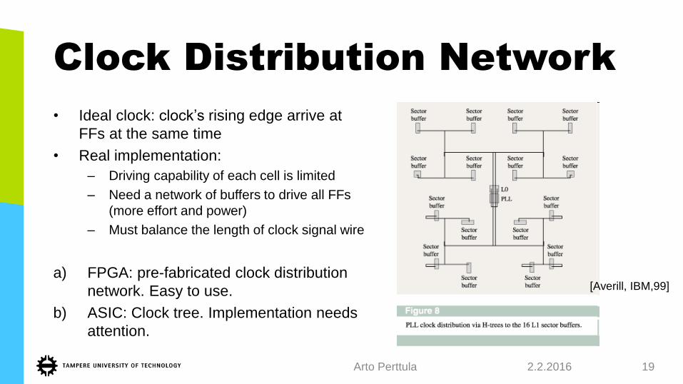
Clock Distribution Network
• Ideal clock: clock’s rising edge arrive at
FFs at the same time
• Real implementation:
– Driving capability of each cell is limited
– Need a network of buffers to drive all FFs
(more effort and power)
– Must balance the length of clock signal wire
a) FPGA: pre-fabricated clock distribution
network. Easy to use.
b) ASIC: Clock tree. Implementation needs
attention.
2.2.2016 Arto Perttula 19
[Averill, IBM,99]
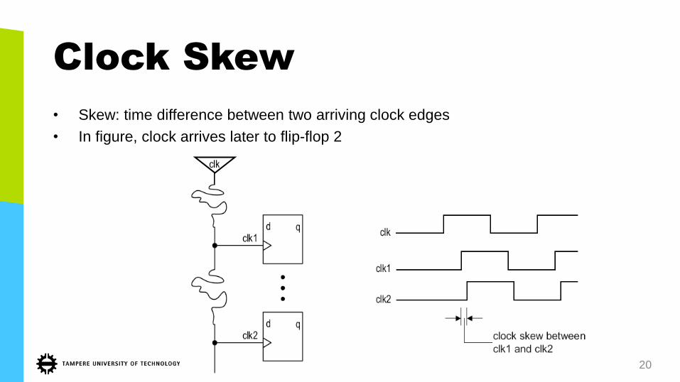
Clock Skew
• Skew: time difference between two arriving clock edges
• In figure, clock arrives later to flip-flop 2
2.2.2016 Arto Perttula 20

Skew Affects Timing Analysis
1. Setup time constraint (impact on maximum clock rate)
2. Hold time constraint (impact on minimum combinational delay)
• One gets easier due to skew, and the other gets harder
Arto Perttula 21
Note that clk signal can also be driven from
bottom to top, and the following analysis
example would change accordingly

2.2.2016 22
Tcq +Tnext(min) > Thold + Tskew
Tcq +Tnext(max)< Tc – Tsetup + Tskew
Tskew = clock skew
Tcq = DFF clock-to-Q
Tnext = comb. delay
Thold = DFF hold time
Tsetup = DFF setup time
Requirements:
In general, we must assume ±Tskew
Larger skew could violate
the hold time of dff2
Example when clk2 comes after clk1

Clock Skew
• Clock skew normally has negative impact on synchronous
sequential circuit
– Regarding either setup or hold constraints
1. Effect on setup time constraint: must increase clock period =>
lower clock frequency
2. Effect on hold time constraint: may violate hold time when D
changes too fast after clock edge
– Can only be fixed during physical synthesis: re-route clock; re-place
register and combinational logic; add artificial delay logic
• Rule of thumb: Skew within 10% of clock period tolerable
2.2.2016 Arto Perttula 23
MULTIPLE-CLOCK SYSTEM
2.2.2016 Arto Perttula 24
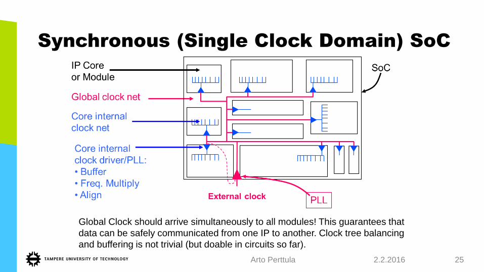
Synchronous (Single Clock Domain) SoC
2.2.2016 Arto Perttula 25
Global Clock should arrive simultaneously to all modules! This guarantees that
data can be safely communicated from one IP to another. Clock tree balancing
and buffering is not trivial (but doable in circuits so far).

SoC with Multiple Clock Domains
2.2.2016 Arto Perttula 26
Sometimes different domains may physically overlap -- Especially in FPGA
Communication between domains (e.g. data[31:0]) needs special attention.
Within one domain there is no problem.

Why Multiple Clocks
1. Inherent multiple clock sources
– E.g., external communication links require their own frequencies
2. Circuit size
– Clock skew increases with the number of FFs in a system
3. Design complexity
– E.g., as system with 16-bit 20 MHz processor, 1-bit 100 MHz serial interface, 1 MHz I/O controller
a) No need to optimize them all to run at 100 MHz (simpler + cheaper)
b) No need to run everything at 1 MHz (better performance)
4. Power consideration
– Dynamic power proportional to switching frequency
– Use lowest frequency allowed for each IP
– Especially useful when combined with lowered voltage!
2.2.2016 Arto Perttula 27


Derived vs. Independent Clocks
a) Independent clocks:
– Relationship between clocks is unknown
b) Derived clocks:
– A clock is derived from another clock signal (e.g., different clock rate or phase)
– Relationship is known
• Typical implementation is done with clocks that are integer multiples of each other
• E.g., 200 MHz bus and 800 MHz processor
– Logic for the derived clock should be separated from regular logic and manually
synthesized (e.g., special delay line or PLL)
– A system with derived clock can still be treated and analyzed as a synchronous
system
2.2.2016 Arto Perttula 29

GALS
• Globally Asynchronous, Locally Synchronous system
– Partition a system into multiple independent subsystem with different clock domains
– Design and verify subsystem in same clock domain as a synchronous system
– Design special interface between clock domains
• Can be handled with the interconnection between subsystems
• Relaxes generation of global clock tree
30
Video encoding application Main control Wireless communication
CPU CPU CPU
CPU Accl. CPU
HIB
I BR
IDG
E
CPU CPU CPU
CPU CPUH
IBI B
RID
GE
CPU CPU
CPU CPU
CPU CPU
CPU CPU CPU
CPU
CPU
Security module User Interface
Re-usable multiprocessorsub-systems
NiosII
HIBI Segment
HIBI Segment
HIBI Segment
HIBI Segment
HIB
I BR
IDG
EH
IBI B
RID
GE
HIBI Segment
…
…
AES
Displ.
DataRAM
BootROM
NiosTo
HIBI…
Nios IIprocessor
coreExternalinterface
Avalon

Taxonomy of Multiple Clock Domains
31

META-STABILITY AND
SYNCHRONIZATION FAILURE
2.2.2016 Arto Perttula 32

Timing Analysis of a
Synchronous System
• To satisfy setup time constraint:
a) Signal from a register
– Controlled by clock
– Adjust clock period to avoid setup time violation
– Adjust routing to avoid hold time violation
b) Signal from external input
– Same as a) if the external input comes from another synchronous
subsystem
– Otherwise, have to deal with the occurence of setup and hold time
violation
2.2.2016 Arto Perttula 33

Asynchronous Input
• We have no clue when the button is pressed, i.e., we cannot
guarantee that it will adhere to the setup constraints
• Setup/hold time violations inevitably occur
2.2.2016 Arto Perttula 34
D Q
clk
Button press

Asynchronous Input (2)
• Signal arrives to flip-flops at slightly different times due to routing delays
• In the example, the button’s rising edge arrives to upper DFF just before clock edge, and just after it to the lower one
• On the next cycle, also the lower DFF captures it OK
• HOWEVER, a state machine may have gone awry already!
– E.g., one-hot state machine leaves one state but does not enter any other state, i.e., ”zero-hot”, or it is in two states
simultaneously, or it may…
• Something needs to be done
2.2.2016 Arto Perttula 35
D Q
clk
Button press
D Q
0 →1 →1 0 →1 →1
0 →0 →1

Asynchronous Input (3)
• Output of first DFF goes metastable at some point
• The following DFF’s fo not necessarily interpret it the same way!
– Upper one thinks value is 1
– Lower one thinks it is 0
• This is why it is so hard to measure: logic gates and analyzer tool might interpret it differently
– Logic analyzer’s probe will also cause some load which changes behaviour a little
2.2.2016 Arto Perttula 36
D Q
clk
Button press
D Q
0,0,0 →1 →1 0 →1 →1
0,0,0 →0 →1
D Q
0,0 →meta →1

Two Asynchronous Clock Domains
• clk1 frequency ~33 MHz (30 ns period)
• clk2 frequency 62.5 MHz (16 ns period)
• tsetup, thold = 0.1 ns
• The clk2 DFF setup/hold time violations inevitably occur
– Event in D2 is too close to rising edge of clk2
• Similar to previous case
2.2.2016 Arto Perttula 37
Comb D Q
clk1
D Q
clk2

Asynchronous Failures
38

Main Effect of Setup Violation
2.2.2016 Arto Perttula 39

Long Delay / Metastability
due to Data Conflicts
2.2.2016 40
Metastability Is Hard to Detect
• MTBF can be several months. Most of the time everything works and then something does not
– How to reproduce that?
• Basic RTL simulation cannot notice metastability!
– May be captured at accurate gate-level simulation
• DFF’s are instantiated as components and they have checking mechanisms
• Too tedious and slow to be feasible
• Logic analyzers connected to real chip cannot detect metastability well
– The metastable signal values (somewhere between 0 and 1) are assumed either ’0’ or ’1’
– Logic analyzer may interpret them differently than real logic
– Slow path might be detected if one uses very high sampling frequency
Synchronizers must be tested separately and on real HW
– Automatically send large amounts of known values and check all
– Note! Absence of evidence is not evidence of absence. However, already a single error shows that the
synchronizer is broken.
2.2.2016 Arto Perttula 41

What Happens after Failure?
a) Output of FF becomes 1 (sampled old input value)
b) Output of FF becomes 0 (sampled new input value)
c) FF enters metastable state, the output exhibits an ”in-between” value
– FF eventually ”resolves” to one of stable states
• Sometimes it is claimed that FF starts to oscillate, but that is very rare in CMOS technology (i.e., in the mainstream
technology)
– The resolution time is a random variable with distribution function
– τ is a decay time constant
• Determined by electrical characteristics of the FF
• Typically today a fraction of a nanosecond
• The propability that metastability persists beyond Tr (i.e., cannot be resolved within Tr)
Arto Perttula Tr
P(Tr)

MTBF(Tr)
• Synchronization failure: An FF cannot resolve the metastable
condition within the given time
• MTBF – Mean Time Between (here: synchronization) Failures
– Basic criterion for metastability analysis
– Frequently expressed as a function of Tr
• Tr is the time allowed for the FF to recover some state (0/1) after a
metastable event
• Note that then there is Tr less time for the combinatorial logic (Tr
affects TCQ, i.e., it is in critical path)
2.2.2016 Arto Perttula 43

Arto Perttula 44
• MTBF computation
fclk = FF clock frequency
fd = Data input change rate
ω = susceptible time window
Propability that the flip flop does not resolve within Tr τ is a DFF’s decay time constant
Average number of
synchronization failures
in second
Mean time between
(synch.) failures

2.2.2016 Arto Perttula 45
E.g. 0.13m technology, danger window ω =66ps, decay constant =33 ps, fclk=200MHz, input change rate fd=0.1fclk
Tr [ns] MTBF Column1
0.5 14.4 sec
0.7 1.7 hours
0.9 30.6 days
1.1 36.0 years
1.3 1.5E+04 years
1.5 6.6E+06 years
1.7 2.8E+09 years
1.9 1.2E+12 years
2.1 5.2E+14 years
2.3 2.2E+17 years
2.5 9.6E+19 years
2.7 4.1E+22 years
2.9 1.8E+25 years
3.1 7.5E+27 years
3.3 3.2E+30 years
Note that the examples in the course book are valid but for much older technology
Age of Earth ~1010 years
R.Ginosar’s
”guesstimate”,
See references

Xilinx FPGA Real-Life
• CLB Flip-Flops, Virtex II Pro (0.13u, 1.5Vcc)
2.2.2016 Arto Perttula 46

2.2.2016 Arto Perttula 47
http://www.altera.com/literature/an/an042.pdf
NOTE: Figures for CPLDs,
quite old technology
=Tr

MTBF with Multiple DFFs
• 1/MTBF = λ = failure rate of the component
• E.g., MTBF = 100 years, failure rate of 1% per year
– The shown MTBF calculation is for one DFF only
• For multiple DFFs, error-free behaviour means that none of DFFs misbehaves
MTBF(s) = 1/(1/MTBF(s0)+1/MTBF(s1)+ … +1/MTBF(sn))
– where MTBF(sn)= MTBF of synchronizer i
• E.g., MTBF(s0) = 1000 years and MTBF(s1) = 500 years, then MTBF(s) = 333 years
• E.g., MTBF(s0) = 1000 years, having 20 of them reduces MTBF to 1/(20*1/1000) =
1000/20 = 50 years
2.2.2016 Arto Perttula 48

Observations
• MTBF is statistical average, not a guarantee
– Large calculated MTBF gives you some confidence but, however, may not give the correct
result in reality
• Parameters ω and depend on implementation technology
• Only Tr can be adjusted in practical design
– Slack time for the FF, before the value is required to be stable, can be increased => lower
frequency
• MTBF is extremenly sensitive to Tr
– Tr is in the exponent of MTBF equation
– Small variation in Tr can lead to large swing in MTBF
– Good: synchronization failure can be easily avoided by providing additional resolution time
– Bad: minor modification can introduce synchronization failure
2.2.2016 Arto Perttula 49

Observations (2)
• Incorrect assumption: MTBF is 100 years, everything’s fine
– MTBF should be thinked over the whole amount of chips
– If 100 000 chips are sold with this design, then 100 000/100 devices fail every year 2.7 per day you are out of
the business!
• MTBF should always be calculated
• Remember that there are other components that might fail also
– E.g., memories and logic due to radiation
• For reliable figures, one mus obtain the ω and values of the used technology
• Metastability
– Basically an “analog” phenomena
– Resolution time is not exact but probability function
– Resolved value is random
– Cannot be easily modeled or simulated in gate level (only ‘X’)
– Cannot be easily observed or measured in physical circuit (e.g., logic analyzer might not recognize and possibly long
MTBF = 3 month/chip)
2.2.2016 Arto Perttula 50

Estimating MTBF via Measurement
• Sample the synchronizer output Qd on both rising and falling edge of clock
• Qf samples first - after half a cycle - and then Qr samples after full cycle
• If values differ, Qd was very probably metastable at the halfway of the cycle
• Cannot detect metastability that resolves fast, i.e., Tr<Tcycle/2
– Perhaps using multiple phase-shifted clocks for sampling would detect also these
Arto Perttula 51

Timing Example
• clkB is faster here
• Qs is simplest test signal
– Just toggles on every clkA cycle, i.e., divides it’s frequency by 2
• Orange star indicates when Qs changes too close to clkB
– Hold time violation
• Qd goes metastable
– Resolves to 1 within cycle
• Lower DFF samples Qd first
– Qd is metastable value and Qf stays 0 here
• Upper DFF samples the resolved value of Qd correctly (Qr=1)
• xor output rises always when Qf != Qr
• Error is detected only when xor output is 0 at falling edge of
clkB (blue star)
2.2.2016 Arto Perttula 52

SYNCHRONIZER
2.2.2016 Arto Perttula 53

Synchronization Circuit
• Synchronizes an asynchronous data input with system clock
• In general
– No physical circuit can prevent metastability
– We cannot avoid it, we have to live with it
– Design should be ”metastability-tolerant”, since it cannot be ”metastability-free”
• Synchronizer just provides enough time for the metastable condition to be
”resolved”
• Later examples assuming these values for MTBF calculations
– ω = 66ps, = 33 ps, fd = 0.1fclk, fclk=200MHz (hence Tc = 5ns)
– Tsetup = very small, say 0.1 ns
2.2.2016 Arto Perttula 54

55

Wrong: No Synchronizer
• Tr = 0
• MTBF(0) = 3.8 us
• Donnerwetter! Dies instantly!
2.2.2016 Arto Perttula 56
Note: in book, the example MTBFs are counted with older technology, whereas in these slides with the values presented earlier
Don’t do this.
clk

Wrong: One-FF Synchronizer
• Tr = Tc – (Tcomb + Tsetup)
• Tr depends on Tc , Tsetup and Tcomb
– Tc varies with system specification (clock period)
– Tcomb varies with circuit, synthesis (gate delay), placement & routing (wire delay)
• E.g.,
– Tr = 5ns – (Tcomb + 0.1ns ) = 4.9ns – Tcomb
– Tcomb = 4 ns, Tr = 0.9 ns; MTBF(0.9) = 31 days
• Not a reliable design
57
Don’t do this.

The Right-Way: Two-FF
Synchronizer
• Add an extra FF to eliminate Tcomb
– Tr = Tc – Tsetup
– Tr depends on Tc only!
– Asynchronous input delayed by two clock cycles
• E.g.,
– Tr=5ns – 0.1ns= 4.9ns; MTBF(4.9)=3.7*1051 years
• Most commonly used synchronizer
• Some ASIC technologies ay have ”metastability-hardened” DFF cell (large area)
2.2.2016 Arto Perttula clk

Super-Safe: Multi-Stage
Synchronizer
• Add extra stages to increase resolution time
– Tr = (nstages-1)*(Tc – Tsetup)
– Asynchronous input delayed by three clock cycles
– Each stage adds one clock cycle more to resolution time
– Increasingly unlikely that all go metastable
• E.g.,
– Tr =2*(5ns – 0.1ns); MTBF(9.8)=1.1*10116 years
• Extremely safe but still practical
2.2.2016 Arto Perttula 59

2.2.2016 Arto Perttula 60
Allowed tesolution time Tr can be interpret as ”slack time before combinatorial logic”
Tr = Tc – (Tcomb + Tsetup)
Tr = Tc – Tsetup
Tr = 2(Tc – Tsetup) )

6 Cases of Synchronizer
Timing
2.2.2016 Arto Perttula 61
[R. Ginosar, Metastability and Synchronizers : A
Tutorial, IEEE D&T Comp, Sep/Oct 2011]
Case a = Q1 goes 1 as wished f = Q1 goes metastable, goes randomly to 1 and resolves to 1; looks like case a
b = Q1 misses 1 at first but rises at cycle 2 d = Q1 goes metastable, stays 0 and resolves to 0; looks like case b
c = Q1 metastable
but resolves to 1
within one cycle
d = Q1 metastable
and goes first 1 but
then resolves to 0
Hence, Q2 rises all cases, but the
cycle is either on 2 or 3. Note that
D1 stays stable long enough

Beware of WRONG Two-FF
Synchronizers!
• Asynchronous input contains both data and control
• This does NOT work…
• Recall: we do not know what state the flip-flop gets after metastable event
– The data may get corrupted
– Note that some bits may be sampled correctly while some will go metastable
Arto Perttula
CL FF3
clock
FF2
Async
input FF1
© 2003-2006 Ran Ginosar
n
1 n+1 ctrl
data
other_clk

Proper Use of Synchronizer
• Use a glitch-free signal for
synchronization
– The signals between clock domains must
come from a register
• Synchronize a signal in a single place
– Separate synchronization logic to a
different module
• Avoid catastrophic parallel synchronizers
• Reanalyze the synchronizer after each
design change
Arto Perttula
...

AN ENABLE TICK THAT
CROSSES CLOCK DOMAIN
2.2.2016 Arto Perttula 64

Signals That Cross Clock Domains
• Need synchronizer
– Just ensures that the receiving system does not enter a
metastable state
– Does not guarantee the ”function” of the received signal. The
value may be wrong but at least it is truly 0 or 1
• Consideration
1. One signal
2. Multiple signals (”bundled data”)
2.2.2016 Arto Perttula 65
Domain-Crossing of an
Enable Signal
• An enable tick – pulse that denotes new data
– To be sampled on a single clock edge
– E.g., enable input of a counter; read/write signal of a FIFO buffer
– Can also be used to retrieve bundled data
• We need an edge detector in order to know that a new data has
arrived
– Don’t even think of using ’event construct in VHDL. Grrr!
• Depending on frequencies, the enable tick is either
a) wide – from slow to fast domain
b) narrow – from fast to slow domain
2.2.2016 Arto Perttula 66

”Wide” Enable Signal
• From a slow clock domain to a fast clock domain (e.g., 1 MHz to 10 MHz)
• Typical user I/O has very wide pulse from the digital circuit’s point of view
2.2.2016 Arto Perttula 67

”Narrow” Enable Signal
• From a fast clock domain to a slow clock domain (e.g., 10 MHz to 1
MHz)
• The enable pulse is too narrow to be detected
– Very short pulse occurs somewhere between the clock edges
– It is never stored into synchronizing DFF
• We need to ”stretch” the pulse
– Cannot be done by a normal sequential circuit
– Do not use ”tricks”
The right way to do: handshaking circuit
2.2.2016 Arto Perttula 68

HANDSHAKING
Transferring data between clock domains reliably
2.2.2016 Arto Perttula 69

General Problems in Data
Communication
• How to know that a new data is coming/data has been read?
• How to know that receiver is ready?
• Does the sending system have prior knowledge about the processing speed
of receiving system?
• How to control the rate of data (or number of enable ticks) between two
clock domains? (e.g., 10 MHz system to 1 MHz system)
• What if data was corrupted?
• Handshaking scheme
1. Use a feedback signal
2. Make minimal assumption about the receiving system
2.2.2016 Arto Perttula 70

Wide Pulse Problem Visualized
2.2.2016 Arto Perttula 71

A Solution
• We need handshake control signals
1. Write_request (tx → rx, downstream)
2. Acknowledge (rx → tx, upstream)
– These are transition-triggered, not level triggered!
• Change in signal state implies new data, not the level of the signal (0 or 1)
– So called Two-phase handshake protocol
• Does not depend on the relative clock frequencies
• Only the 1-bit control signal is synchronized! Never use synchronizers for data
– Control and data may arrive at slightly different time on opposite sides of a clock edge! The
other is sampled whereas the other is not. Paha paha!
– Data is fed directly to the another clock domain’s registers
2.2.2016 Arto Perttula 72

The Right Way:
• Data load is directed by
multiplexer (or flip-flop
enable)
• Only 1-bit control
synchronized
• Data has lots of time to
stabilize while the control
signal is being synchronized
• Note that the multiplexer
select signal may need more
complex logic
2.2.2016 Arto Perttula 73
Control D Q D Q
D Q 0
1 Data
clk_b
Asynchronous
Synchronous to clk_b
Edge
det

A Block Diagram for
Handshake Transfer
2.2.2016 Arto Perttula 74

Transition Triggered Example:
Send Two Values 0xf and 0x2
75
Why Data Is Not Synchronized? How Do
We Make Sure It Is Not Corrupted?
• When data is issued to the rx, it is not read in to any register yet
• Data is read to the target domain’s input register after the control signal has been received reliably
– Synchronization delay
• Data could be issued before the request to be sure
– How long it takes for the data to propagate to receiver? Is wire delay in data larger than in request signal?
– If request signal is sent first and the rx block is very fast, out data y not be arrived yet when sampled
• However, this is not very typical
– Usually issuing them on the same edge suffices if the required timing constraints have been set (i.e., make
sure that data is valid before request)
• We can be sure that when request is detected by rx, the data is stabilized
– If data is stable, it cannot violate the FF timings, so it is safe to read to the FFs
2.2.2016 Arto Perttula 76

Why the Proposed Method Is Safe?
• E.g., the tx sends data, it sets signal request 0 → 1
• If it drives the synchronizer to metastability, it resolves to ’0’ or ’1’ (provided
large enough MTBF)
a) If it resolves to ’0’ then
• No change detected in signal
• However, in next clock cycle, the FF is loaded with the right value
• one clock cycle delay on transfer
b) If it resolves to ’1’ then
• Change detected, proceed as normally
• No chance for erraneous interpretation of data transmission/acknowledge
2.2.2016 Arto Perttula 77

Observations
• Performance, clock cycles per transfer:
– 0-1 cc for Rx synchronizer metastability resolution
– 3 cc for Rx to issue ack (2 for synch, 1 for putting ack to outreg)
– 0-1 cc for Tx synchronizer metastability resolution
– 2 cc for Tx to synchronize ack
– 5-7 clock cycles per transfer (compare to 1 in totally synchronous)
– Domain crossing is slow!
• Other methods for data transfer
1. FIFO (syncronization needed for empty and full status signal)
• May perform quite well for large data chunks
2. Shared memory (synchronization needed for arbitration circuit)
3. Dual-port memory (meta-stable condition may occur in the internal arbitration circuit)
– These also need the synchronization! Domain crossing is still tricky and slow!
2.2.2016 Arto Perttula 78

Observations (2): Don’t Over-Optimize
• It is not beneficial to fine-tune all frequencies
• E.g., increasing tx clock 475 500 MHz
– Needs synchronizers
– ~5% increase in Tx processing power
– ~5x decrease in transfer rate Tx Rx
• The overall performance might be better with lower frequency
– Same phenomenon happens with supply voltages and voltage converters/regulators
• One must analyze when multiple clocks pays off
– Depends on frequencies (e.g., 400 vs. 500 MHz)
– Depends on computation vs. communication ratio (e.g., ops/sent_byte)
79

Gray FIFO
• Pointers use gray code: only a single bit changes at a time
– Hence, the whole pointer can be synchronized although it has multiple bits. Ingenious!
Arto Perttula [R. Ginosar, Metastability and Syncronizers : A
Tutorial, IEEE D&T Comp, Sep/Oct 2011]

Gray FIFO (2)
• Each write (read) increments write pointer (read pointer)
• Pointers wraparound from n-1 to 0
• Number of FIFO slots must be power of 2: 2 slots,4,8…
• Status is decided by comparing pointer, e.g., if read_ptr == write_ptr, then FIFO is empty
• Synchronization adds latency in some cases
– It might take two cycles before consumer notices that data has been written, if FIFO was empty before that
– Performance degrades, but everything works
• When pointer values are not close to each other, both producer and consumer can operate FIFO
on their own maximum frequency
• Synchronized pointer is always smaller than or equal to real value
– Writer and reader will stop before overflow or underflow will occur
2.2.2016 Arto Perttula 81

Gray FIFO (3): Multiple Writes
• What happens if a fast writer puts many data words into FIFO before reader notices anything? Or
vice versa?
– wptr is incremented many times and consequently many bits will change
• Let’s assume that FIFO is empty and 4 words are written
– wptr = 000 → 001, 011, 010, 110
• The trick is that the old Q value has no impact: even if all Q bits change, that alone will not cause
metastability
• Problem occurs if multiple D bits change near clock edge at synchronizer’s first DFF
– Only the last increment 010 → 110 may happen near clock edge
– Only 1 D-bit changes (uppermost)!
a) No problem, if syncronizer succeeds
b) If synchronizer fails, the output will be the older value 010
• That means 3 instead of 4
• Reader might have to pause for one clock cycle which causes minor loss of performance but no corruption
2.2.2016 Arto Perttula 82

• Planned (not necessarily realized) functionality:
• en_q asserted at the rising edge of en_in
• en_q the synchronized
• en_strobe then clears stretcher
• en_q may last over two clock cycles and thus an edge-detector is needed
• Note that these kind of structures are sometimes presented. However, they are case-specific and not portable and
may introduce several not-so-easy to find bugs. Avoid these structures.
– What if en_strobe changes near en_in’s edge?
2.2.2016 Arto Perttula 83
Asynchronous reset shall not be a part
of the implementation functionality!!
”A not-so-clever trick”

Erroneous Greedy Path in
Edge Detector
• ”Why bother waiting for 3 cycles. I’ll tweak it a little bit…”
• Typical mistake
• Incorrect implementation
84
Only a single FF in this signal’s path, Tr very short
en_r will go metastable and therefore en_out will also. Don’t do this.
en_r

DERIVED CLOCKS
2.2.2016 Arto Perttula 85

Data Transfers between
Derived Clock Domains
• If the clocks are in the same phase, the data transmission between derived
clock domains is somewhat easier
– System is still synchronous, the flops won’t go metastable
– This can be guaranteed by statistical timing tools, as in globally synchronous
system having only one clock
• Normal level-sensitive logic enable can be used
– The signal must be observable (no pulse stretching)
• However, this still poses challenges to clock tree distribution
• E.g., Tx clk = 10 MHz (period = 100 ns), Rx clk 40 MHz (period = 25 ns)
• Design a circuit that narrows the 100 ns pulse to 25 ns pulse
2.2.2016 Arto Perttula 86
Derived Clock Synchronizer:
Implementation
• Applicable when knowing the relative difference beforehand
– E.g., when both clocks come from the same PLL, the oscillator noise
and drift affect both of them equally
• Use a counter to detect the last clock cycle
– More time for data to stabilize
• Counter is naturally clocked at the higher of the two frequencies
• E.g., 4x difference in frequencies: use 0-to-3 counter
– When 3 is reached, a one clock cycle ’1’ pulse is AND’ed with the actual
we-signal form the tx
• Denoted with we_narrow in the next slide’s example
2.2.2016 Arto Perttula 87

Example of Derived Clock
Synchronization with Slow Pulse
2.2.2016 Arto Perttula 88

Derived Clock Synchronizer:
Implementation
• When not knowing the relative difference
• First, we have to know which clock is faster
1. Use a feedback loop with edge detector to know whenever the
slower clock has changed its state
– Both ends send a feedback signal that toggles every rising clock edge
(=half frequency w.r.t. their own clock)
2. At rx, set one cycle long ’1’-pulse (faster clock period) at the
beginning of each slower clock edge
– Slower device may send as often as it wishes
2.2.2016 Arto Perttula 89

Example of Derived Clock Synchronization, TX Slower But
Actual Difference Not Known at Design Time

’This and That’ -chronous
• Synchronous – system is coordinated with global clock
• Isochronous – the time interval between two significant moments is constant or an integer-multiple of it
– Isochronous transfer – can start at random time w.r.t. to rx, but bits in transfer come with fixed interval
• Asynchronous – no global clock
• Mesochronous – tx and rx have the same frequency, but unknown phase
– Same clock source, but undefined clock skew due to routing
• Plesiochronous – tx and rx are almost synchronized
– Both have their own oscillator with matching frequencies and all variance is within specified limits
– Nevertheless, the mismatch accumulates, the phase drifts
2.2.2016 91

Clock Uncertainties
[B. Nikolić, EE241 - Spring 2004
Advanced Digital Integrated Circuits, Lecture 21,
http://bwrcs.eecs.berkeley.edu/Classes/icdesign/ee241_s04/lectures/Lecture21-Timing.pdf]

RESET SYNCHRONIZATION
2.2.2016 Arto Perttula 93

Problem with Reset Timing
• Reset must fulfill reset recovery and removal time constraints
– No change just before or after rising clock edge
• E.g., the output of a flip-flop can go metastable when the reset is deasserted close to the
rising edge of the clock and the output to the flip-flop must change
• Most problems occur when exiting reset state – not entering it

Problem with Reset (2)
• Reset signal has some delay from input pin to the flip-flops
– Delay varies between flip-flops
• Asynchronous reset signal may arrive just before clock edge to some flip-flops and just after edge to some
– More likely the further apart the flip-flops are
• May go undetected, unless logic expects that certain flip-flops ”tick together”
– E.g., bits from FSM state register
– E.g., two counters should produce exactly the same values, e.g., to generate pseudo-random numbers
95

Must Synchronize the Reset Also
• Designer must guarantee that reset signal does not change near
clock edge
Ensure that internal reset signal goes inactive at beginning of clock
period
1. Synchronize reset input
2. The reset has a full cycle to propagate to all flip-flops
• Loose constraint: Domain reset delay < Domain TC (clock period)
– All the registers+combinational logic must be stabilized within a clock
period
2.2.2016 Arto Perttula 96

Reset Synchronizer
• On chip reset:
1. Most FFs are set or reset (so called follower DFF, e.g., in shift register, can omit reset)
2. Clocks are started
3. Reset is carefully removed
• Reset state is entered immediately but exited just after clock edge in the synchronizer below
• Global reset should be glitch-free (e.g., analog debounce logic)
97

Synchronous vs. Asynchronous
• Be careful with terminology!
1. Asynchronous vs. synchronous reset of DFF
– Using the dedicated input or D-input of DFF
– Note that latter requires running clock. Ensure that reset is active long enough (>PLL lock
time)
2. Asynchronous vs. synchronized reset signal
– Using chip’s external input directly (with undefined timing characteristics) vs. via
synchronizer logic
• We will always synchronize the reset signal to the clock
– It is not that big deal whether it is connected dedicated asynchronous rst/clr input or D
• Was this unclear enough?
2.2.2016 Arto Perttula 98
Conclusions
• Asynchronous inputs to synchronous system violate FFs timing constraints FFs go
metastable
• Two flip-flops are required to synchronize asynchronous inputs
– Only control is synchronized, not data
• Clock domain crossing requires special handshaking structures
– The data throughput between two asynchronous clock domains is considerably less than
between synchronous ones (~6x less)
– Synchronous derived clocks are also possible
• Clock routability problems
• MTBF/#chips must be on range of > 104 years at least in order to call design ”safe”
• Reset must also be synchronized
2.2.2016 Arto Perttula 99