city research onlinesouvik ghosh is with the department of school of mathematics, computer science...
TRANSCRIPT
City, University of London Institutional Repository
Citation: Ghosh, S. and Rahman, B. M. (2016). An Innovative Straight Resonator Incorporating a Vertical Slot as an Efficient Bio-Chemical Sensor. IEEE Journal on Selected Topics in Quantum Electronics, 23(2), doi: 10.1109/JSTQE.2016.2630299
This is the accepted version of the paper.
This version of the publication may differ from the final published version.
Permanent repository link: https://openaccess.city.ac.uk/id/eprint/16546/
Link to published version: http://dx.doi.org/10.1109/JSTQE.2016.2630299
Copyright and reuse: City Research Online aims to make research outputs of City, University of London available to a wider audience. Copyright and Moral Rights remain with the author(s) and/or copyright holders. URLs from City Research Online may be freely distributed and linked to.
City Research Online: http://openaccess.city.ac.uk/ [email protected]
City Research Online

For Review O
nly
An Innovative Straight Resonator Incorporating a Vertical
Slot as an Efficient Bio-Chemical Sensor
Journal: Journal of Selected Topics in Quantum Electronics
Manuscript ID JSTQE-CON-PS2017-06432-2016.R2
Manuscript Type: Contributed
Date Submitted by the Author: 05-Oct-2016
Complete List of Authors: Ghosh, Souvik; City University, School of Mathematics, Computer Science and Engineering Rahman, B M A; City University London, EEIE; City University London, Electrical & Electronic Engineering
Keyword: Finite element methods, Integrated optics, Resonators
JSTQE
For Review O
nly
IEEE JOURNAL OF SELECTED TOPICS IN QUANTUM ELECTRONICS,
1
Abstract— A compact and integrated label-free refractometric
bio-chemical sensor based on silicon-on-insulator (SOI) is
proposed and comprehensively studied at the telecommunication
wavelength of λ = 1550 𝒏𝒎. This device incorporated a three
dimensional (3D) Fabry-Perot cavity in the nano-scale regime
with maximum footprint area around 470 × 473 𝒏𝒎2. A
resonance shift (𝚫𝝀𝒓𝒆𝒔) of 5.2 𝒏𝒎 is reported for an ultra-thin
(5 𝒏𝒎) bio-layer sensing. Besides, an improved maximum
sensitivity (𝐒 = 820 𝒏𝒎/𝑹𝑰𝑼) is also achieved for bulk refractive
index change in surroundings. As a chemical sensor, very low
detection limit (𝐃𝐋 = 𝟔. 𝟏 × 𝟏𝟎−𝟔 𝑹𝑰𝑼) also can be possible to
achieve by this device. All the numerical investigations and
optimizations were carried out in frequency domain by a
numerically efficient and rigorous full vectorial H-field based two
dimensional (2D) and three dimensional (3D) finite element
methods (FEM). A 3D-FEM code is developed and used to find
out the wavelength dependencies of the resonator. Possibility of
easy CMOS fabrication and integration opportunities make this
structure as a prospective and efficient lab-on-chip device.
Index Terms — Finite Element Method, Integrated Optics,
Resonator, Sensors.
I. INTRODUCTION
Following the initial work by Graham Reed, Richard Soref
first proposed the fabrication of silicon waveguides in a
silicon-on-insulator (SOI) wafer in the telecom wavelength
range, 1200 - 1600 𝑛𝑚 [1]. The high-refractive-index contrast
of SOI structures leads to the higher degree of light
confinement and guidance through the silicon layer. This
property can make the silicon waveguides and resonators to be
the basic building blocks of compact photonic integrated
circuits (PIC). Over the last two decades, silicon technology
has attracted considerable attentions due to its potential low-
cost by exploiting the CMOS fabrication technology,
developed for electronics, which can also be used by the
photonics industries.
Light confinement in low-index slot section was first
reported in 2004 [2] and since then SOI based slot waveguide
became an intriguing area of research. The boundary condition
Souvik Ghosh is with the Department of School of Mathematics, Computer
Science and Engineering, City University London, Northampton Square, London, EC1V 0HB, UK (e-mail: [email protected]).
B. M. A. Rahman is with the Department of School of Mathematics,
Computer Science and Engineering, City University London, Northampton Square, London, EC1V 0HB, UK (e-mail: [email protected]).
of electromagnetic field demands normal component of
electric flux density (D) must be continuous at the dielectric
interface, which results a high magnitude electric field (E)
discontinuity at the same interface. These characteristics lead
to a strong field enhancement in the low-index slot region. As
a result, the slot waveguides becoming an attractive choice as
a refractive index (RI) based biological and chemical sensors.
By combining the slot properties with resonating devices, a
higher sensitivity can be achieved. Combination of slot
configuration with ring resonator was first investigated and
fabricated by Barrios et al. [3], [4] on a Si3N4 – SiO2 platform
with a maximum sensitivity of 212 𝑛𝑚/𝑅𝐼𝑈. An improved
sensitivity of 298 𝑛𝑚/𝑅𝐼𝑈 has also been reported by Claes et
al. [5] for the similar slot waveguide based ring resonator in
SOI platform. These structural devices show significant
improvement of refractive index sensitivity over the
conventional strip waveguide based ring resonator,
demonstrated by K. D. Vos et al. [6]. Integration of Bragg
gratings on SOI platform with promising application in bio
and chemical sensing has also been reported [7], [8]. The
conventional strip and rib waveguide based Bragg gratings use
the evanescent field tails for the sensing, thus exhibiting a
lower sensitivity with high quality (Q) factor. Wang et al.
recently proposed an improved slot waveguide based Bragg
sensors with sensitivity as high as 340 𝑛𝑚/𝑅𝐼𝑈 around 1550
𝑛𝑚 wavelength with the help of enhanced light matter
interaction into the slotted region [9]. Recently, an improved
bulk detection sensitivity (380 𝑛𝑚/𝑅𝐼𝑈) of porous silicon ring
resonator for biosensing applications has been reported by G.
A. Rodrigues et al. [10]. Other optical bio-chemical sensors
have incorporated microdisk resonator [11], photonic crystal
cavities [12], [13] and Mach-Zehnder interferometers [14],
[15].
In this paper, we present a detailed theoretical and
numerical investigations of three dimensional single
vertically-slotted resonator structure in a SOI platform. An in-
house numerically efficient and rigorous three dimensional
full vectorial H-field based finite element method (3D-FEM)
is developed and used to obtain the modal solutions at the
particular resonating wavelength. Initially, optimizations of
design parameters, such as the width (W), height (H) and slot
width (Ws) are carried out by a two dimensional full-vectorial
H-field based Finite Element Method (2D-FEM).
Subsequently the resonating modal fields, sensitivity (S) and
detection limit (DL) of this optimized device have been
An Innovative Straight Resonator Incorporating
a Vertical Slot as an Efficient Bio-Chemical
Sensor
Souvik Ghosh and B. M. A. Rahman, Fellow, IEEE
Page 1 of 9 JSTQE
123456789101112131415161718192021222324252627282930313233343536373839404142434445464748495051525354555657585960
For Review O
nly
IEEE JOURNAL OF SELECTED TOPICS IN QUANTUM ELECTRONICS,
2
calculated by the 3D-FEM. Interestingly, we observed an
effective change in sensitivity from 635 𝑛𝑚/𝑅𝐼𝑈 to 820
𝑛𝑚/𝑅𝐼𝑈 depending on the position of the perfect electric wall
(PEW) in the device. As the detection limit (DL) of the sensor
device is inversely related to the sensitivity (S), the changes in
the sensitivity due to metal boundary position also makes a
noticeable change in the detection limit (DL). Such a high
sensitivity and detection limit achieved by proposed device
can be invaluably important in the field of chemical sensing.
We have validated this phenomenon with sucrose solution at
ambient temperature (20°𝐶). It has been noticed that bio-
molecules become transparent in the near infrared region
(NIR). Hence the dominated optical absorption is governed by
the water solvent which shows a dip in the absorption
spectrum at 1550 𝑛𝑚 wavelength. Hence we selected the
operating wavelength of the device for bio-chemical sensing
around 1550 𝑛𝑚, the standard telecommunication wavelength,
which adds an extra advantage of availability of standardized
resources of the telecommunication band to design the nano-
structured sensing setup.
This paper is arranged as follows. In 2nd section, we first
demonstrate a concise mathematical steps of the full vectorial
H-field based three dimensional finite element method (3D-
FEM) for resonating structures. The 3rd section gives the
description of our proposed structure with its geometrical
parameters. In this section, all the design parameters are
optimized by numerically accurate 2D-FEM. In 4th section, we
report the excellent sensing ability of the proposed device as a
bio-chemical sensor. The modal responses at the resonating
wavelength are obtained by using the 3D-FEM code. Finally,
all findings are summarized in the conclusive part.
II. VECTOR FORMULATION OF 3D-FEM
In general, to accomplish the theoretical investigation of a
photonic device it is required to solve the partial differential
equations (PDEs) and in most cases, the equations under
consideration are much complex to be solved by using an
analytical or semi-analytical methods. Solutions of Maxwell’s
equations are the essential part to design and analyze the
integrated photonic waveguides and resonators. For the modal
solutions of waveguide structures, a full vectorial 2D-FEM has
been established as the most efficient approach and our in-
house code developed and refined over last 30 years has been
very effective [16]-[18]. However, to investigate the three
dimensional (3D) optical resonating structures with isotropic
and anisotropic materials, a new full vectorial H-field based
three dimensional Finite Element Method (3D-FEM) is
required. Both the Finite Element (FE) formulations (2D and
3D) are based on a variational formulation which is
comprehensive to solve complex waveguide and resonator
problems with isotropic, anisotropic homogeneous and
inhomogeneous media. For 2D waveguide problems,
variational expressions can present the propagation constants
of the fundamental and higher order quasi-TE and TM modes.
On the other hand, for the 3D resonating structures, variational
expression calculates the resonant frequencies and associated
vectorial mode profiles of the cavity.
Although, E-field, H-field and mixed E+H field
formulations have been proposed [19], here we have
considered the H-field based formulation which shows great
advantages [16]-[18], [20] regarding natural implementation
of the boundary conditions at the dielectric interfaces
compared to other formulations. The natural boundaries
associated with the formulation is that of a perfect electric
walls (PEW), so that the arbitrary conducting guiding walls
can be left free. Besides, the chosen H-field is continuous at
the dielectric interfaces which is convenient for dielectric
resonator problems. Considering the advantage of the
structural symmetry, when available, the necessary boundary
conditions can also be imposed on the boundary interfaces
which increases the accuracy and also decreases the
computational cost.
The full vectorial H-field based 3D-FEM starts from
Maxwell’s two curl equations. The solution region or the
device is discretized into a number of small unstructured
volumetric domain, called elements. We used first order
tetrahedral elements for computational simplicity. Firstly, the
H-field within each element is calculated and then
interrelation of the field distributions in other elements are
followed such that the field becomes continuous across the
inter-element boundaries. The H-field for a single element can
be derived from the total sum of the product of shape function
vector and field value at each node of the element. As the
variational formulation consists of Maxwell’s two curl
equations, hence their Euler equation follow the Helmholtz’s
equation but do not necessarily satisfy the divergence equation
(𝑑𝑖𝑣. 𝑩 = 0). This causes the presence of spurious solutions
spread all over the eigenvalue spectrum along with the real
physical modes. Like the 2D-FEM, the appearance of spurious
modes are also true for a 3D-FEM. To avoid the presence of
spurious solutions, we followed the similar penalty method as
reported earlier [17]. We introduced an additional functional
with a weighting factor for the penalty number 𝛼 in the full
vectorial H-field formulation. The Euler equation of the
modified functional (𝑱𝑒) satisfy the Maxwell’s divergence
equation (𝑑𝑖𝑣. 𝑩 = 0).
Here the functional 𝑱𝑒 describes the numerical errors that
occurs due to unstructured discretization, 𝑘02 denotes the
eigenvalue, 𝜖�̂� and �̂�𝑟 are the relative permittivity and
permeability tensor of the medium, respectively. By
minimizing the functional in the equation (1) by 𝜕
𝜕{𝑯}𝑒 𝑱𝑒 = 0,
the overall numerical error is minimized and the compact form
of the eigenvalue equation becomes
𝑱𝑒 = [∫ (𝛁 × 𝑯)∗ ⋅ 𝜖�̂�−1 (𝛁 × 𝑯) 𝑑𝑣 + 𝛼 ∫ (𝛁 ⋅ 𝑯)∗(𝛁 ⋅ 𝑯) 𝑑𝑣
𝑣𝑣] − 𝑘0
2[∫ 𝑯∗ ⋅ �̂�𝑟𝑯 𝑑𝑣𝑣
] (1)
Page 2 of 9JSTQE
123456789101112131415161718192021222324252627282930313233343536373839404142434445464748495051525354555657585960
For Review O
nly
IEEE JOURNAL OF SELECTED TOPICS IN QUANTUM ELECTRONICS,
3
Here 𝑘0 is the wavenumber, 𝜔 is the angular frequency. The
equation (2) is the modified form of often quoted Berk’s
formulation [19]. The eigenvector corresponding to the
eigenvalue shows the quasi-TE and TM mode profiles inside
the resonator cavity.
III. DEVICE GEOMETRY
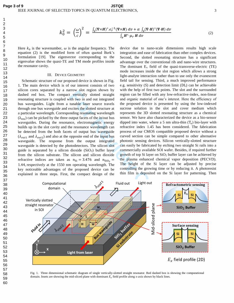
Schematic structure of our proposed device is shown in Fig.
1. The main device which is of our interest consists of two
silicon cores separated by a narrow slot region shown by
dashed red box. The compact vertically slotted straight
resonating structure is coupled with two in and out integrated
bus waveguides. Light from a tunable laser source travels
through one bus waveguide and excites the slotted structure at
a particular wavelength. Corresponding resonating wavelength
(λres) can be picked by the three output facets of the in/out bus
waveguides. During the resonance, electromagnetic energy
builds up in the slot cavity and the resonance wavelength can
be detected from the both facets of output bus waveguide
(𝜆𝑜𝑢𝑡1 and 𝜆𝑜𝑢𝑡2) and also at the opposite end of the input bus
waveguide. The response from the output integrated
waveguide is detected by the photodetectors. The silicon slot
guide is separated by a silicon dioxide (SiO2) buffer layer
from the silicon substrate. The silicon and silicon dioxide
refractive indices are taken as nSi = 3.476 and nSiO2=
1.44, respectively at the 1550 nm operating wavelength. The
key noticeable advantages of the proposed device can be
explained in three steps. First, the compact design of the
device due to nano-scale dimensions results high scale
integration and ease of fabrication than other complex devices.
Second, the slotted resonating structure has a significant
advantage over the conventional rib and nano-wire structures.
The dominant Ex field of the quasi-transverse-electric (TE)
mode increases inside the slot region which allows a strong
light-analyte interaction rather than to use only the evanescent
field tail for sensing. Third, a much improved performance
e.g. sensitivity (S) and detection limit (DL) can be achievable
with the help of first two points. The slot and the surrounded
region can be filled with any low-refractive-index, non-linear
and organic material of one’s interest. Here the efficiency of
the proposed device is presented by using the low-indexed
sucrose solution in the slot and cover medium which
represents the 3D slotted resonating structure as a chemical
sensor. We have also characterized the device as a bio-sensor
dipped into water, where a 5 nm ultra-thin (Ts) bio-layer with
refractive index 1.45 has been considered. The fabrication
process of our CMOS compatible proposed device without a
curved section can be simple compared to other alternative
photonic sensing devices. Silicon vertically-slotted structure
can easily be fabricated by etching two straight Si rails into a
commercially available SOI wafer. Besides, if required further
growth of top Si layer on SiO2 buffer layer can be achieved by
the plasma enhanced chemical vapor deposition (PECVD).
The height of the Si layer can be adjusted by precise
controlling the growing time or by reducing it. A photoresist
thin film is deposited on the Si layer for patterning. Then
Fig. 1. Three dimensional schematic diagram of single vertically-slotted straight resonator. Red dashed box is showing the computational
domain. Insets are showing the mid-sliced plane with dominant 𝐸𝑥 field profile along x-axis shown by black lines.
𝑘02 = (
𝜔
𝑐)
2=
∫ (𝛁×𝑯)∗.𝜖𝑟−1(𝛁×𝑯)
𝑣 𝑑𝑣 + 𝛼 ∫ (𝛁⋅𝑯)∗(𝛁⋅𝑯) 𝑑𝑣
𝑣
∫ 𝑯∗⋅𝜇𝑟 𝑯 𝑑𝑣𝑣
(2)
Page 3 of 9 JSTQE
123456789101112131415161718192021222324252627282930313233343536373839404142434445464748495051525354555657585960
For Review O
nly
IEEE JOURNAL OF SELECTED TOPICS IN QUANTUM ELECTRONICS,
4
reactive ion-etching (RIE) is used to make the both Si strips
with a slot region in between them.
The rigorous investigation of design parameters,
calculation of dominant and non-dominant field components
and profiles for the fundamental quasi-TE and TM modes, due
to the presence of sensing material with different refractive
index values, are of great importance when designing a
sensing device. Our in-house two dimensional (2D) [16]-[18]
and newly developed three dimensional (3D) Finite Element
Method (FEM) are used as numerical tools to obtain the modal
solutions of the Si slotted resonator. The 3D slotted resonator
is a short length of straight vertical slot waveguide. As a
result, a part of the design parameters can be estimated by
using the computationally efficient fully vectorial rigorous
2D-FEM.
A 5 nm sensing layer (Ts) over the Si core and also inside
the slot region is considered for bio-molecule detection, as
shown in Fig. 1 bottom inset. The Si core width (W), slot
height (H) and slot width (Ws) are optimized for different
parameters, such as the power confinements into low-indexed
slot and 5 nm sensing bio-layer into the slot region,
normalized power density (NPD) and effective index (𝛥𝑛𝑒𝑓𝑓)
change. The 𝛥𝑛𝑒𝑓𝑓 is the change in the effective index (𝑛𝑒𝑓𝑓)
due to the presence of 5 nm molecular bio-ad layer.
Fig. 2. Optimization of Si core width (W) depending on confinement factor
(Γ). Total slot confinement (Γ𝑠𝑙𝑜𝑡−𝑡𝑜𝑡𝑎𝑙) and confinement of 5 𝑛𝑚 sensing
layer into slot versus Si core width (𝑛𝑚) for a fixed Si core/slot height of 220
𝑛𝑚 and 324 𝑛𝑚. Slot width (W) is 100 𝑛𝑚. The cover medium, slot region and the sensing layer into slot are filled with water.
Figure 2 shows variation of the power confinement in the
slot (Γ𝑠𝑙𝑜𝑡−𝑡𝑜𝑡𝑎𝑙) and 5 nm sensing layer (Γ𝑠𝑙𝑜𝑡 𝑠𝑒𝑛𝑠𝑖𝑛𝑔 𝑙𝑎𝑦𝑒𝑟)
with the Si core width (W) by red and blue lines, respectively.
The solid and dashed lines show the power confinement
variations for two different sets of Si core heights, H = 220
𝑛𝑚 and 324 𝑛𝑚, respectively. For both the cases, the slot
width (Ws) is constant, Ws = 100 𝑛𝑚. When the core is wide
enough, the power confinement into Si core is large and this in
turn results a low confinement into slot region. It can be
observed that with the reduction of the core width (W), the
confinements increase in the slot and reach their maximum
values at W = 190 𝑛𝑚 and W = 220 𝑛𝑚 for H = 324 𝑛𝑚 and
H = 220 𝑛𝑚, respectively. Subsequently a rapid fall of
confinement in slot region is also noticeable with the further
reduction of W. The power confinement of sensing layer into
slot region (Γ𝑠𝑙𝑜𝑡 𝑠𝑒𝑛𝑠𝑖𝑛𝑔 𝑙𝑎𝑦𝑒𝑟) also shows similar trend as that
of Γ𝑠𝑙𝑜𝑡−𝑡𝑜𝑡𝑎𝑙. To study the effect of core height, the variations
of total slot confinement (Γ𝑠𝑙𝑜𝑡−𝑡𝑜𝑡𝑎𝑙), normalized power
density (NPD) in the slot and change of effective index
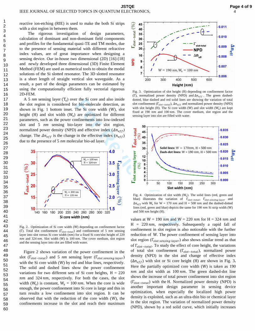
(Δ𝑛𝑒𝑓𝑓) with slot or Si core height (H) are shown in Fig. 3.
Here the partially optimized core width (W) is taken as 190
𝑛𝑚 and slot width as 100 𝑛𝑚. The green dashed-dot line
shows the increase of total power confinement into slot region
(Γ𝑠𝑙𝑜𝑡−𝑡𝑜𝑡𝑎𝑙) with the H. Normalized power density (NPD) is
another important design parameter in sensing device
optimization, when especially the localized high power
density is exploited, such as an ultra-thin bio or chemical layer
in the slot region. The variation of normalized power density
(NPD), shown by a red solid curve, which initially increases
Fig. 3. Optimization of slot height (H) depending on confinement factor
(Γ), normalized power density (NPD) and Δ𝑛𝑒𝑓𝑓 . The green dashed-
dotted, blue dashed and red solid lines are showing the variation of total
slot confinement (Γ𝑠𝑙𝑜𝑡−𝑡𝑜𝑡𝑎𝑙), Δ𝑛𝑒𝑓𝑓 and normalized power density (NPD)
with slot height (H). The Si core width (W) and slot width (Ws) are kept
fixed at 190 𝑛𝑚 and 100 𝑛𝑚. The cover medium, slot region and the sensing layer into slot are filled with water.
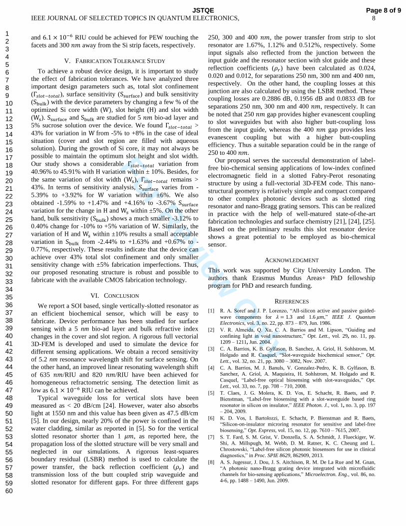
Fig. 4. Optimization of slot width (Ws). The solid lines (red, green and
blue) illustrates the variation of Γ𝑠𝑙𝑜𝑡−𝑡𝑜𝑡𝑎𝑙, Γ𝑠𝑙𝑜𝑡 𝑠𝑒𝑛𝑠𝑖𝑛𝑔 𝑙𝑎𝑦𝑒𝑟 and
Δ𝑛𝑒𝑓𝑓 with Ws for W = 170 𝑛𝑚 and H = 500 𝑛𝑚 and the dashed-dotted
lines (red, green and blue) depicts the same for 190 𝑛𝑚 Si strip width (W)
and 500 𝑛𝑚 height (H).
Page 4 of 9JSTQE
123456789101112131415161718192021222324252627282930313233343536373839404142434445464748495051525354555657585960

For Review O
nly
IEEE JOURNAL OF SELECTED TOPICS IN QUANTUM ELECTRONICS,
5
as slot height (H) increases and reaches a maximum value at H
= 300 𝑛𝑚. But with the further increment of H, the normalized
power density (NPD) decreases. Here the variation of effective
index shift (𝛥𝑛𝑒𝑓𝑓) due to the presence of 5 nm thick
molecular bio-ad layer with H is a key design parameter and
shown by a blue dashed line. The variation of 𝛥𝑛𝑒𝑓𝑓 with the
H shows a strong correlation with the Γ𝑠𝑙𝑜𝑡−𝑡𝑜𝑡𝑎𝑙 variation.
Both the parameters increase, as the slot height (H) increases.
Although, generally SOI structures with H = 220 𝑛𝑚 is more
widely used, however, as it is shown here that higher heights
yield better sensors, so optimized slot height for our device is
taken as 500 𝑛𝑚, which would be easy to fabricate [21], yields
Γ𝑠𝑙𝑜𝑡−𝑡𝑜𝑡𝑎𝑙 = 41.965% and 𝛥𝑛𝑒𝑓𝑓 = 0.0104.
So far we have kept the slot width (Ws) fixed at 100 𝑛𝑚, as
it was theoretically optimized for slot waveguide based
homogeneous sensor [22] and also successfully used in label-
free slot based ring resonator for bio sensing application [5].
However, the slot width (Ws) variation with optimized W
(190 𝑛𝑚) and H (500 𝑛𝑚) shows the maximum Γ𝑠𝑙𝑜𝑡−𝑡𝑜𝑡𝑎𝑙 =
42.405% at a slightly wider slot width, Ws = 130 𝑛𝑚, shown
by a red dashed-dotted line in Fig. 4. Here the confinement of
sensing layer into slot (Γ𝑠𝑙𝑜𝑡 𝑠𝑒𝑛𝑠𝑖𝑛𝑔 𝑙𝑎𝑦𝑒𝑟) with green dashed-
dotted line and effective index change (Δ𝑛𝑒𝑓𝑓) with blue
dashed-dotted line shows a strong correlation and both of them
decrease with the increment of slot width (Ws). As a very
small slot width may not easy to fabricate, hence total
confinement into slot (Γ𝑠𝑙𝑜𝑡−𝑡𝑜𝑡𝑎𝑙) can be taken as a critical
factor. A further investigation of Γ𝑠𝑙𝑜𝑡−𝑡𝑜𝑡𝑎𝑙 variation with W
by keeping Ws and H fixed at 130 𝑛𝑚 and 500 𝑛𝑚,
respectively, gives only a small change in earlier optimized W
and shows maximum confinement (Γ𝑠𝑙𝑜𝑡−𝑡𝑜𝑡𝑎𝑙 = 43.751%) at
W = 170 𝑛𝑚. The red, green and blue solid lines in Fig. 4
shows the Γ𝑠𝑙𝑜𝑡−𝑡𝑜𝑡𝑎𝑙 , Γ𝑠𝑙𝑜𝑡 𝑠𝑒𝑛𝑠𝑖𝑛𝑔 𝑙𝑎𝑦𝑒𝑟 and Δ𝑛𝑒𝑓𝑓 variations
with slot width (Ws), for W = 170 𝑛𝑚 and this set suggests a
new value, Ws = 110 nm when Γ𝑠𝑙𝑜𝑡−𝑡𝑜𝑡𝑎𝑙 becomes maximum.
As there was not much difference in Γ𝑠𝑙𝑜𝑡−𝑡𝑜𝑡𝑎𝑙 for W = 170
and 190 nm and a few 𝑛𝑚 extra slot width which may also be
convenient for fabrication, we have finalized the optimized
slot width as 130 nm. Hence all the optimized 2D design
parameters of slot structure can be taken as, W = 170 𝑛𝑚, H =
500 𝑛𝑚 and Ws = 130 𝑛𝑚 when the cover medium and the
slot region is considered to be filled up with aqueous solution
of refractive index 1.33. The full vectorial 2D-FEM has again
been applied to determine the effective index (𝑛𝑒𝑓𝑓) of the
optimized structure and this value is 1.63827. The
corresponding 2D 𝐸𝑥 field profile is shown in Fig. 5.
Throughout these 2D-FEM simulations, the structure is
discretized with 1,280,000 first order triangular elements.
Next, we design the vertically slotted resonating structure
using the optimized W, H and Ws (Fig. 1) discussed above.
The slot supports longitudinal modes that resonance at a
specific wavelength (𝜆𝑟𝑒𝑠) as,
𝜆𝑟𝑒𝑠 = 2𝐿.𝑛𝑒𝑓𝑓
𝑚 (3)
Here 𝑚 is the longitudinal mode order inside the cavity
(𝑚 = 1, 2, 3 … …) and 2L denotes the round trip length of the
electromagnetic wave in the resonator. As the fundamental
mode is expected to be more stable and sensitive than other
higher order modes, we calculate the length (L) of the slot
resonator using equation (3) for the fundamental mode (𝑚 =
1). Finally, all the device dimensions have been considered
can be summarized as, Si core width (W) = 170 n𝑚, slot
height (H) = 500 𝑛𝑚, slot width (Ws) = 130 𝑛𝑚 and the device
length (L) = 473.06 𝑛𝑚 for the expected resonating
wavelength (𝜆) of 1550 𝑛𝑚.
In and out straight bus waveguides can be used to connect
the resonator cavity with the light source and detectors. A
phase matched Si strip waveguide of width 218 𝑛𝑚 and height
500 𝑛𝑚 can be used as bus, shown in Fig. 1. The gap between
resonator and adjacent bus waveguide can be within the range
of 250 𝑛𝑚 to 400 𝑛𝑚 to achieve a good coupling.
Alternatively, to maintain the phase matched condition, a slot
waveguide having the same dimensions: W = 170 𝑛𝑚, H = 500
𝑛𝑚 and Ws = 130 𝑛𝑚 can also be used as bus waveguide.
Here a 300 to 400 𝑛𝑚 gap can be useful to couple light wave
in between resonator and in/out bus waveguide.
Fig. 5. Enhanced 𝐸𝑥 field into slot region for optimized device dimensions: Si
strip width (W) = 170 𝑛𝑚, height (H) = 500 𝑛𝑚 and Ws = 130 𝑛𝑚. 2D-FEM code is used for simulation.
IV. PERFORMANCE ANALYSIS
In a resonating structure the self-consistent field gets
confined and oscillates at a particular frequency, hence the
basic performance investigation requires complete three
dimensional field analysis of the quasi-TE and TM modes
inside the resonating structure. For the present work, a
dedicated rigorous and full vectorial H-field based three
dimensional finite element (3D-FEM) code is developed to
solve the problem. We divided the performance analysis into
two stages: (1) surface sensing with an ultra-thin bio-
molecular layer covers the sensor surface (see Fig. 1, bottom
inset) and (2) homogeneous refractometric sensing (see Fig. 1,
top inset), where sensitivity for bulk refractive index change in
surrounding medium is considered.
Page 5 of 9 JSTQE
123456789101112131415161718192021222324252627282930313233343536373839404142434445464748495051525354555657585960

For Review O
nly
IEEE JOURNAL OF SELECTED TOPICS IN QUANTUM ELECTRONICS,
6
A. Surface Sensing
The first stage of our investigation is based on
homogeneous bio-sensing where we have considered a thick
bio-ad layer (refractive index 1.45) on both the Si strips and
inside the slot region. The cover medium is filled with
aqueous solution (𝑛𝑤𝑎𝑡𝑒𝑟 = 1.33). For detail analysis we have
also considered different thickness of sensing layers ranging
from 5 𝑛𝑚 to 50 𝑛𝑚. During the 3D-FEM simulations, we
have verified the numerical accuracy by considering over
456817 first order tetrahedral elements in the computational
domain of 1.47 𝜇𝑚 (along x) × 0.47306 𝜇𝑚 (along y) × 1.5
𝜇𝑚 (along z). A resonating wavelength shift from 1537.21 𝑛𝑚
to 1542.38 𝑛𝑚 was observed due to the presence of ultra-thin
5 𝑛𝑚 sensing layer with refractive index of 1.45. Hence the
refractive index change in the sensing layer causes a resonance
shift (𝛥𝜆𝑟𝑒𝑠) of 5.2 nm for surface sensing. We have also
studied the surface sensitivity (𝑆𝑠𝑢𝑟𝑓𝑎𝑐𝑒) for different bio-layer
thickness. The 𝛥𝜆𝑟𝑒𝑠 linearly increases with the thickness of
sensing layer. This is shown by a red solid line in Fig. 6,
depict a strong linear resonance shift (𝛥𝜆𝑟𝑒𝑠) with bio-layer
thickness change (𝛥𝑡). The blue stars denote the variation of
surface sensitivity 𝑆𝑠𝑢𝑟𝑓𝑎𝑐𝑒 = (𝛥𝜆𝑟𝑒𝑠/𝛥𝑡) against different
bio-layer thickness, plotted in a high resolution scale. A small
reduction of 𝑆𝑠𝑢𝑟𝑓𝑎𝑐𝑒 can be observed with the increment bio-
layer thickness. Our simulation shows almost similar
sensitivity as reported in [5] but in our case with a simpler
straight structure.
B. Bulk Refractive Index Sensing
The second stage of sensitivity investigation follows the
detection of bulk refractive index change in the cover and the
slot region. Aqueous sucrose solutions with different
concentrations are used over the sensing device. The refractive
index of sucrose-water solution for different sucrose
concentration at ambient temperature (20°𝐶) are taken from
[23]. Two different cases are considered during simulation
process: (1) the slot region and cover medium are completely
filled with the fluid, and (2) only cover medium is filled with
sucrose solution and the narrow slot region is filled with air
bubble. In the present formulation, the natural boundary
condition is that of a perfect electric wall (PEW). If the
structure is enclosed inside a metal box, then we do not need
to impose the boundary condition. However, for an open type
resonating structure, the computational boundary should be
away from the resonating structure. The bulk sensitivity
(Sbulk) also depends on the position of computational or
physical electric wall. Figure 7 depicts the bulk refractive
Fig. 7. Bulk refractometric sensitivity (S) analysis of vertically single
slotted waveguide with optimized design parameters at 1550 𝑛𝑚. The slope of the curve denotes the sensitivity of the slot waveguide while the
cover medium is filled with sucrose solution.
Fig. 6. Surface sensing of the proposed device with optimized design
parameters. The red line depicts a linear resonance wavelength shift
(Δ𝜆𝑟𝑒𝑠) for different bio-layer thickness of refractive index 1.45. The blue
stars denote the surface sensitivity (𝑆𝑠𝑢𝑟𝑓𝑎𝑐𝑒) variation with bio-layer
thickness ranging from 5 𝑛𝑚 to 50 𝑛𝑚.
Fig. 8. Bulk sensitivity (Sbulk) analysis of the proposed device.
Resonating wavelength shift (𝑛𝑚) versus refractive index variation
(Δ𝑛𝑠𝑢𝑐𝑟𝑜𝑠𝑒) of sucrose solution at ambient temperature (20°𝐶). The solid lines illustrate the resonating wavelength shift when the perfect electric
walls (PEW) are touching the end faces of Si core. The dashed lines
present the same when the PEWs are 300 𝑛𝑚 away from both end faces of the Si core. The slope of each linear curve represents the sensitivity
(Sbulk) for the filled and empty conditions.
Page 6 of 9JSTQE
123456789101112131415161718192021222324252627282930313233343536373839404142434445464748495051525354555657585960

For Review O
nly
IEEE JOURNAL OF SELECTED TOPICS IN QUANTUM ELECTRONICS,
7
index sensitivity of the optimized single vertically-slotted
waveguide simulated by 2D-FEM. The variation of
normalized effective index change (Δ𝑛𝑒𝑓𝑓/𝑛𝑒𝑓𝑓) with
different refractive indices of sucrose solution is presented by
the red solid line. The slope gives us the sensitivity Sbulk =(Δ𝑛𝑒𝑓𝑓/𝑛𝑒𝑓𝑓)/𝑅𝐼𝑈 of 1.025 per 𝑅𝐼𝑈. Figure 8 shows the
resonance wavelength shift (Δ𝜆) of the resonating structure as
a function of refractive index of sucrose solution at 20°𝐶. The
solid line shows the variation of resonance wavelength shift
(Δ𝜆) with the change of refractive index of sucrose solution
when the PEWs are placed at both end faces of Si strips. A
strong linear shift is observed, and the slope of the lines i.e.
sensitivity (Sbulk) shows the value of 635 𝑛𝑚/𝑅𝐼𝑈 and 335
𝑛𝑚/𝑅𝐼𝑈 for the fully filled and for the case of empty slot (a
case arises when sensing liquid may not enter the slot region),
respectively. A significant improvement can be observed of
the proposed device sensitivity compared to the other devices
reported earlier [3]-[10]. The dashed line also shows a linear
shift of resonance wavelength (Δ𝜆) when the PEWs are
positioned at 300 𝑛𝑚 away from both the end faces of the Si
core strips. Corresponding 3D iso-surface profiles of confined
𝐸𝑥 fields for both cases are shown in Fig. 9. The 3D iso-
surface field profiles are generated by the post-processing of
the eigenvectors obtained from complete device simulation by
the developed 3D-FEM. Fluid-Si surface contact increases
when the boundary walls are kept away from the Si strip’s end
faces. As a result, a greater sensitivity has been observed,
illustrated by the blue and the green dashed lines with slope
820 𝑛𝑚/𝑅𝐼𝑈 and 683 𝑛𝑚/𝑅𝐼𝑈 for filled and empty slot
region, respectively. These values are much higher and shows
a considerable improvement over the theoretically and
experimentally investigated sensing devices reported so far
[3]-[10]. Besides the spectral shift i.e. sensitivity, detection
limit (DL) is another important parameter to illustrate the
efficiency of the sensor to detect and quantify the properties of
the deposited sample of interest. The DL can be estimated
from the sensitivity (Sbulk) and the sensor resolution (R)
as, 𝐷𝐿 = 𝑅/𝑆𝑏𝑢𝑙𝑘. The resolution of the device is controlled
by the wavelength resolution (𝜆𝑟𝑒𝑠𝑜𝑙𝑜𝑡𝑖𝑜𝑛) of the light source
and sensitivity (Sbulk) is the slope of the curves in Fig. 8. If we
consider a laser source having wavelength resolution of 5 pm
[6], a minimal detectable refractive index of 7.9 × 10⁻⁶ RIU
Fig. 9. The dominant 𝐸𝑥 field (2D and 3D) confined into straight single slotted resonator with optimized design parameters at the telecommunication
wavelength. Field profiles are generated by post-processing of eigenvectors of resonating wavelength (𝜆𝑟𝑒𝑠 being an eigenvalue), (a) shows the 𝐸𝑥 field
profile of slot resonator on an x-z sliced plane and (b) depicts the 3D iso-surface profile of 𝐸𝑥 field. The PEWs are considered at both end faces of the Si
cores. (c) 3D iso-surface profile of confined 𝐸𝑥 field when the boundary PEWs are 300 𝑛𝑚 and 500 𝑛𝑚 away from both end faces and side faces of Si strips,
respectively. Full vectorial 3D-FEM is used for complete resonating structure simulation.
Page 7 of 9 JSTQE
123456789101112131415161718192021222324252627282930313233343536373839404142434445464748495051525354555657585960
For Review O
nly
IEEE JOURNAL OF SELECTED TOPICS IN QUANTUM ELECTRONICS,
8
and 6.1 × 10⁻⁶ RIU could be achieved for PEW touching the
facets and 300 𝑛𝑚 away from the Si strip facets, respectively.
V. FABRICATION TOLERANCE STUDY
To achieve a robust device design, it is important to study
the effect of fabrication tolerances. We have analyzed three
important design parameters such as, total slot confinement
(Γ𝑠𝑙𝑜𝑡−𝑡𝑜𝑡𝑎𝑙), surface sensitivity (Ssurface) and bulk sensitivity
(Sbulk) with the device parameters by changing a few % of the
optimized Si core width (W), slot height (H) and slot width
(Ws). Ssurface and Sbulk are studied for 5 𝑛𝑚 bio-ad layer and
5% sucrose solution over the device. We found Γ𝑠𝑙𝑜𝑡−𝑡𝑜𝑡𝑎𝑙 >
43% for variation in W from -5% to +8% in the case of ideal
situation (cover and slot region are filled with aqueous
solution). During the growth of Si core, it may not always be
possible to maintain the optimum slot height and slot width.
Our study shows a considerable Γ𝑠𝑙𝑜𝑡−𝑡𝑜𝑡𝑎𝑙 variation from
40.96% to 45.91% with H variation within ± 10%. Besides, for
the same variation of slot width (Ws), Γ𝑠𝑙𝑜𝑡−𝑡𝑜𝑡𝑎𝑙 remains >
43%. In terms of sensitivity analysis, Ssurface varies from -
5.39% to +3.92% for W variation within ±6%. We also
obtained -1.59% to +1.47% and +4.16% to -3.67% Ssurface
variation for the change in H and Ws within ±5%. On the other
hand, bulk sensitivity (Sbulk) shows a much smaller -3.12% to
0.40% change for -10% to +5% variation of W. Similarly, the
variation of H and Ws within ±10% results a small acceptable
variation in Sbulk from -2.44% to +1.63% and +0.67% to -
0.77%, respectively. These results indicate that the device can
achieve over 43% total slot confinement and only smaller
sensitivity change with ±5% fabrication imperfections. Thus,
our proposed resonating structure is robust and possible to
fabricate with the available CMOS fabrication technology.
VI. CONCLUSION
We report a SOI based, single vertically-slotted resonator as
an efficient biochemical sensor, which will be easy to
fabricate. Device performance has been studied for surface
sensing with a 5 nm bio-ad layer and bulk refractive index
changes in the cover and slot region. A rigorous full vectorial
3D-FEM is developed and used to simulate the device for
different sensing applications. We obtain a record sensitivity
of 5.2 nm resonance wavelength shift for surface sensing. On
the other hand, an improved linear resonating wavelength shift
of 635 𝑛𝑚/RIU and 820 𝑛𝑚/RIU have been achieved for
homogeneous refractometric sensing. The detection limit as
low as 6.1 × 10⁻⁶ RIU can be achieved.
Typical waveguide loss for vertical slots have been
measured as < 20 dB/cm [24]. However, water also absorbs
light at 1550 nm and this value has been given as 47.5 dB/cm
[5]. In our design, nearly 20% of the power is confined in the
water cladding, similar as reported in [5]. So for the vertical
slotted resonator shorter than 1 𝜇𝑚, as reported here, the
propagation loss of the slotted structure will be very small and
neglected in our simulations. A rigorous least-squares
boundary residual (LSBR) method is used to calculate the
power transfer, the back reflection coefficient (𝜌𝑟) and
transmission loss of the butt coupled strip waveguide and
slotted resonator for different gaps. For three different gaps
250, 300 and 400 𝑛𝑚, the power transfer from strip to slot
resonator are 1.67%, 1.12% and 0.512%, respectively. Some
input signals also reflected from the junction between the
input guide and the resonator section with slot guide and these
reflection coefficients (𝜌𝑟) have been calculated as 0.024,
0.020 and 0.012, for separations 250 nm, 300 nm and 400 nm,
respectively. On the other hand, the coupling losses at this
junction are also calculated by using the LSBR method. These
coupling losses are 0.2886 dB, 0.1956 dB and 0.0833 dB for
separations 250 nm, 300 nm and 400 𝑛𝑚, respectively. It can
be noted that 250 𝑛𝑚 gap provides higher evanescent coupling
to slot waveguides but with also higher butt-coupling loss
from the input guide, whereas the 400 𝑛𝑚 gap provides less
evanescent coupling but with a higher butt-coupling
efficiency. Thus a suitable separation could be in the range of
250 to 400 𝑛𝑚.
Our proposal serves the successful demonstration of label-
free bio-chemical sensing applications of low-index confined
electromagnetic field in a slotted Fabry-Perot resonating
structure by using a full-vectorial 3D-FEM code. This nano-
structural geometry is relatively simple and compact compared
to other complex photonic devices such as slotted ring
resonator and nano-Bragg grating sensors. This can be realized
in practice with the help of well-matured state-of-the-art
fabrication technologies and surface chemistry [21], [24], [25].
Based on the preliminary results this slot resonator device
shows a great potential to be employed as bio-chemical
sensor.
ACKNOWLEDGMENT
This work was supported by City University London. The
authors thank Erasmus Mundus Areas+ PhD fellowship
program for PhD and research funding.
REFERENCES
[1] R. A. Soref and J. P. Lorenzo, “All-silicon active and passive guided-
wave components for 𝜆 = 1.3 and 1.6 𝜇𝑚,” IEEE J. Quantum Electronics, vol. 3, no. 22, pp. 873 – 879, Jun. 1986.
[2] V. R. Almeida, Q. Xu, C. A. Barrios and M. Lipson, “Guiding and
confining light in void nanostructure,” Opt. Lett., vol. 29, no. 11, pp. 1209 – 1211, Jun. 2004.
[3] C. A. Barrios, K. B. Gylfason, B. Sanchez, A. Griol, H. Sohlstrom, M.
Holgado and R. Casquel, “Slot-waveguide biochemical sensor,” Opt.
Lett., vol. 32, no. 21, pp. 3080 – 3082, Nov. 2007.
[4] C. A. Barrios, M. J. Banuls, V. Gonzalez-Pedro, K. B. Gylfason, B. Sanchez, A. Griol, A. Maquieira, H. Sohlstrom, M. Holgado and R.
Casquel, “Label-free optical biosensing with slot-waveguides,” Opt.
Lett., vol. 33, no. 7, pp. 708 – 710, 2008.
[5] T. Claes, J. G. Molera, K. D. Vos, E. Schacht, R. Baets, and P. Bienstman, “Label-free biosensing with a slot-waveguide based ring
resonator in silicon on insulator,” IEEE Photon. J., vol. 1, no. 3, pp. 197
– 204, 2009.
[6] K. D. Vos, I. Bartolozzi, E. Schacht, P. Bienstman and R. Baets, “Silicon-on-insulator microring resonator for sensitive and label-free
biosensing,” Opt. Express, vol. 15, no. 12, pp. 7610 – 7615, 2007.
[7] S. T. Fard, S. M. Grist, V. Donzella, S. A. Schmidt, J. Flueckiger, W. Shi, A. Millspugh, M. Webb, D. M. Ratner, K. C. Cheung and L.
Chrostowski, “Label-free silicon photonic biosensors for use in clinical
diagnostics,” in Proc. SPIE 8629, 862909, 2013.
[8] A. S. Jugessur, J. Dou, J. S. Aitchison, R. M. De La Rue and M. Gnan, “A photonic nano-Bragg grating device integrated with microfluidic
channels for bio-sensing applications,” Microelectron. Eng., vol. 86, no.
4-6, pp. 1488 – 1490, Jun. 2009.
Page 8 of 9JSTQE
123456789101112131415161718192021222324252627282930313233343536373839404142434445464748495051525354555657585960
For Review O
nly
IEEE JOURNAL OF SELECTED TOPICS IN QUANTUM ELECTRONICS,
9
[9] X. Wang, S. Grist, J. Flueckiger, N. A. F. Jaeger and L. Chrostowski,
“Silicon photonic slot waveguide Bragg gratings and resonators,” Opt. Express, vol. 21, no. 16, pp. 19029 – 19039, 2013.
[10] G. A. Rodriguez, S. Hu and S. M. Weiss, “Porous silicon ring resonator
for compact, high sensitivity biosensing applications,” Opt. Express, vol.
23, no. 6, pp. 7111 – 7119, 2015.
[11] T. Lipka, L. Wahn, H. K. Trieu, L. Hilterhaus and J. Muller, “Label-free photonic biosensors fabricated with low-loss hydrogenated amorphous
silicon resonators,’’ J. Nanophoton, vol. 7, no. 1, pp. 073793, 2013.
[12] C. Caer, S. F. Serna-Otalvaro, W. Zhang, X. L. Roux and E. Cassan,
“Liquid sensor based on high-Q slot photonic crystal cavity in silicon-on-insulator configuration,’’ Opt. Lett., vol. 39, no. 20, pp. 5792 – 5794,
2014.
[13] D. Yang, C. Wang and Y. Ji, “Silicon on-chip 1D photonic crystal
nanobeam bandstop filters for the parallel multiplexing of ultra-compact integrated sensor array,’’ Opt. Express, vol. 24, no. 15, pp. 16267 –
16279, 2016.
[14] B. J. Luff, J. S. Wilkinson, J. Piehler, U. Hollenbach, J. Ingenhoff and N.
Fabricius, “Integrated optical Mach-Zehnder biosensor,’’ J. Lightwave Technol., vol. 16, no. 4, pp. 583 – 592, 1998.
[15] K. Misiakos, I. Raptis, A. Salapatas, E. Makarona, A. Botsialas, M.
Hoekman, R. Stoffer and G. Jobst, “Broad-band Mach-Zhender
interferometers as high performance refractive index sensors: Theory and monolithic implementation,’’ Opt. Express, vol. 22, no. 8, pp. 8856
– 8870, 2014.
[16] B. M. A. Rahman and J. B. Davies, “Finite-element solution of integrated optical waveguides,” J. Lightwave Technol., vol. 2, no. 5, pp.
682 – 688, Oct. 1984.
[17] B. M. A. Rahman and J. B. Davies, “Penalty function improvement of
waveguide solution by finite element,” IEEE Trans. Microwave Theory Tech., vol. 32, no. 8, pp. 922 – 928, Aug. 1984.
[18] B. M. A. Rahman, “Finite element analysis of optical waveguides,” in
Methods for Optical Guided-Wave Devices: Part I, Modes and
Couplings. W. P. Huang, Ed. Cambridge, MA: EMW Publishing, pp. 187 – 216, 1995.
[19] A. D. Berk, “Variational principles for electromagnetic resonators and
waveguides,” IRE Trans. On Antennas and Propagation, vol. 4, pp. 104
– 111, Apr. 1956.
[20] J.-M. Jin, “The Finite Element Method in Electromagnetics 3rd ed.,”
Wiley-IEEE press 2014.
[21] S. H. Yang, M. L. Cooper, P. R. Bandaru and S. Mookherjea, “Giant
birefringence in multi-slotted silicon nanophotonic waveguides,” Opt.
Express, vol. 16, no. 11, pp. 8306 – 8316, 2008.
[22] F. Dell’Olio and V. M. N. Passaro, “Optical sensing by optimized silicon slot waveguides,” Opt. Express, vol. 15, no. 8, pp. 4977 – 4993,
2007.
[23] Sucrose Conversion Table, FILE CODE 135-A-50, United States
Department of Agriculture (USDA), Jan. 1981.
[24] C. A. Barrios, B. Sanchez, K. B. Gylfason, A. Griol, H. Sohlstrom, M. Holgado and R. Casquel, “Demonstration of slot-waveguide strctures on
silicon nitride / silicon oxide platform,’’ Opt. Express, vol. 15, no. 11,
pp. 6846 – 6856, 2007.
[25] A. Saynatjoki, T. Alasaarela, A. Khanna, L. Karvonen, P. Stenberg, M. Kuittinen, A. Trevonen and S. Honkanen, “Angled sidewalls in silicon
slot waveguides: conformal filling and mode properties,” Opt. Express,
vol. 17, no. 23, pp. 21066 – 21076, 2009.
Souvik Ghosh was born in Kolkata, India. He received his
B.Tech and M.Tech degree in Optics and Optoelectronics
(First class, 1st rank) from Calcutta University (C.U), India in
2012 and 2014, respectively. He is currently pursuing Ph.D
degree at the School of Mathematics, Computer Science and
Engineering, City University London, London, U.K. He is also
a recipient of Erasmus Mundus Areas+ Ph.D fellowship.
His research interests include the application of two
dimensional and three dimensional finite element method in
photonic devices, waveguides as well as resonators. Currently
he is working on the development and application of finite
element method for simulation of complex plasmonic
waveguides and resonators.
B. M. A. Rahman (S’ 80 - M’83 – SM’94 – F’2016) received
his B.Sc Eng. And M.Sc. Eng. Degrees (with distinctions) in
Electrical Engineering from the Bangladesh University of
Engineering and Technology (BUET), Dhaka, Bangladesh, in
1976 and 1979, respectively, and received two gold medals for
being the best undergraduate and graduate students of the
university in 1976 and 1979, respectively. In 1979, he
received a Commonwealth Scholarship and in 1982 obtained a
Ph.D degree in Electronics from University College London,
London, U.K.
From 1976 to 1979, he was a Lecturer in the Department of
Electrical Engineering, BUET. In 1982, he was a Postdoctoral
Research Fellow at University College London. In 1988, he
joined City University London, London, U.K., as a Lecturer,
where he is now a Professor, and leads the research group on
photonics modelling, specialized in the use of rigorous and
full-vectorial numerical approaches to design, analyse, and
optimize a wide range of photonic devices, such as spot-size
converters, high-speed optical modulators, compact bend
designs, power splitters, polarization splitters, polarization
rotators, polarization controllers, THz devices, etc. He is the
author or co-author of more than 500 journal and conference
papers, and his journal papers have been cited more than 3500
times. He is a Fellow of the IEEE, Optical Society of America
(OSA) and SPIE. He is a Chartered Engineer, U.K.
Page 9 of 9 JSTQE
123456789101112131415161718192021222324252627282930313233343536373839404142434445464748495051525354555657585960