cigsse energy envior sci supplementary information · pdf filesupplementary information facile...
TRANSCRIPT
Supplementary Information
Facile Colloidal Synthesis of Quinary CuIn1-xGax(SySe1-y)2 (CIGSSe) Nanocrystal
Inks with Tunable Band Gaps for Use in Low-Cost Photovoltaics
Shu-Hao Chang,a Ming-Yi Chiang,a Chien-Chih Chiang,b Fang-Wei Yuan,a Chia-Yu Chen,a Bo-Cheng Chiu,a Tzu-Lun Kao,a Chi-Huang Laic and Hsing-Yu Tuan*a
a Department of Chemical Engineering, National Tsing Hua University, Hsinchu, Taiwan 30013,
Republic of China.
b Green Energy & Environment Research Laboratories (GEL), Industrial Technology Research
Institute (ITRI), Hsinchu, Taiwan 31040, Republic of China
c Department of Materials Science and Engineering, National Tsing Hua University, Hsinchu,
Taiwan 30013, Republic of China
Corresponding Author
*Hsing-Yu Tuan, Phone: (886)3-5723661; Fax: (886)3-571-5408 E-mail: [email protected]
Electronic Supplementary Material (ESI) for Energy & Environmental ScienceThis journal is © The Royal Society of Chemistry 2011
Experimental Methods
Chemicals: All reagents were used as received. Copper(I) chloride (CuCl; 99.995+%), indium(III) chloride
(InCl3; anyhydrous 99.99%), gallium(III) chloride (GaCl3;99.9999%), elemental sulfur (99.98%),
elemental selenium (99.99%), hexane, toluene, oleylamine (70%) and ethanol (ACS reagent grade,
>99.5%) from Aldrich Chemical Co.
Synthesis of CuIn1-xGax(SySe1-y)2 (CIGSSe) nanocrystals The precursors were carefully weighted using a balance with an uncertainty of ± 0.1 mg (Mettler
Toledo AL204). Reactions were performed using a Schlenk manifold under a purified argon
atmosphere. In a typical synthesis, 0.5 mmol of CuCl (0.0495 g), 0.5 mmol total of InCl3 (0.0000 to
0.1106 g), GaCl3 (0.0000 to 0.0880 g) and 1 mmol total of elemental Se (0.0000 to 0.0790 g) and
elemental S (0.0000 to 0.0320g), 12 ml oleylamine, and a glass-coated stir bar were loaded into a
50-mL three-neck flask. The flask was placed on a magnetic hot plate (Thermo Scientific). The
50-mL flask was then attached to the Schlenk line. The temperature was monitored and controlled
using a thermocouple and a PID temperature controller through the third neck of the flask. The flask
was purged off air and water by argon and bubbling at 130 °C for 1 h in a vigorously stirring. Next,
the system was slowly heated to 265 °C with a 2.3 °C/min raising rate and kept at this temperature
for 1.5 h at vigorous stirring. After reaction, the flask was quenched in a cold water bath to quickly
bring the temperature down. The CIGSSe nanocrystal/oleylamine solution was transferred to a
50-mL centrifuge tube. 10 ml of hexane and 15 ml of ethanol were added to the nanocrystal solution
and centrifuged at 8000 rpm for 10 min. The centrifuge purification procedure was repeated several
times until the supernatant was clear. The nanocrystals were in the precipitate and collected, whereas
the supernatant containing byproducts and unreacted precursor was discarded. The nanocrystals were
redispersed in hexane or toluene for further characterization.
Gram-scale synthesis of CuIn0.5Ga0.5(S0.5Se0.5)2 nanocrystals For gram-scale synthesis, a 500 mL three-neck flas was used as a reactor. The reaction was carried
out in the presence of 5 mmol of CuCl (0.495 g), 2.5 mmol of InCl3 (0.553 g), 2.5 mmol of GaCl3
(0.44 g), 5 mmol of elemental Se (0.395 g), 5 mmol of elemental S (0.161 g), and 120 ml oleylamine
in the 500-mL three-neck flask with a slow heating rate and holding the synthesis at 265 °C for 1.5 h.
The purified procedure was same as the statement before.
CIGSSe-based thin film solar cell fabrication The Mo coated soda lime glass substrates were fabricated by DC magnetron sputtering resulting in
a 500 nm layer. The CIGSSe absorber layer made using CuIn0.7Ga0.3(S0.5Se0.5)2 nanocrystals as a
absorber layer precursor was were spray-coated on the top of Mo substrates by airbrush (KUSING
BD-130, 0.3mm), operated about 20 psig of head pressure. And then, the thin film subsequent
Electronic Supplementary Material (ESI) for Energy & Environmental ScienceThis journal is © The Royal Society of Chemistry 2011

annealed in Ar and Se atmospheres at 450 °C and selenized in a graphite box at 550 °C with rapid
heating. A 80 nm CdS layer was then deposited by a chemical bath deposition (CBD) technique.
The CBD bath contains 183 ml of deionized H2O, 25 ml of 0.015 M CdSO4 solution, 12.5 of 1.5 M
thiourea solution, and 31.25 ml of stock NH4OH (Aldrich). Next, a thin 100 nm high resistivity ZnO
film capped with a ~500 nm high conductivity Al doped ZnO (AZO) layer were deposited by RF
magnetron sputtering. The ZnO film was sputtered in a mixture of 10 % O2 in Ar at sputtering
pressure of 10 mTorr with no intentional heating. The AZO layer was sputtered with neither O2 nor
intentional heating at sputtering pressure of 1 mTorr. After sputtering oxide layers, the final device
was scribed into small area devices with colloidal silver paste as top contact (~0.15 cm2 reduce the
area of Ag electrode).
Characterization
Nanocrystals were characterized using various instruments, including transmission electron
microscopy (TEM), X-ray diffraction (XRD), energy-dispersive X-ray spectroscopy (EDS), X-ray
photoelectron spectroscopy (XPS), UV-vis-NIR absorbance spectrophotometer and cyclic
voltammetry (CV).
TEM sample was prepared by dropping an aliquot of nanocrystals in hexane on a carbon-coated 200
mesh titanium or nickel TEM grids. TEM images were obtained on JEOL JEM-1200 or Hitachi
H-7100 TEM at an accelerating voltage of 120 kV for low resolution imaging and on a Tecnai G2
F20 X-Twin microscope at an accelerating voltage of 200 kV, respectively. The Tecnai G2 F20
X-Twin microscope is equipped with an Oxford INCA EDS detector for EDS analysis. Powder X-ray
diffraction (XRD) analysis was performed on a Rigaku Ultima IV X-ray diffractometer using a Cu
Kα radiation source (λ = 1.54 Ǻ). XRD data were collected for the powders of CuIn1-xGax(SySe1-y)2
nanoparticles on a glass substrate by scanning for 12 h at a rate of 0.016 deg/s. X-ray photoelectron
spectroscopy (XPS) analysis was performed on Kratos Axis Ultra DLD using 500 mm Rowland
circle Al monochromator. For XPS sample preparation, the nanocrystals were drop-casting on a
0.5×0.5 cm wafer in an argon-filled glove box. UV-Vis-NIR absorbance spectra of nanocrystals
dispersion in toluene were obtained by a Hitachi U-4100 UV-vis-NIR spectrophotometer at room
temperature. FTIR Spectra were recorded by dispersing CuIn0.5Ga0.5(S0.5Se0.5)2 nanoparticles in
hexane and placing a small drop of the solution on one of the KBr plates. Place the second KBr plate
on top to get a nice even film. The KBr plates should be carefully cleaned after measurement to
prevent contamination of other samples. Cyclic voltammetry (CV) were recorded on a multi-channel
electrochemical analyzer (Bio-Logic-Science Instruments, VMP3), using glassy carbon as working
electrode, 0.1 M tetrabutylammonium hexafluorophosphate (TBAPF6) dissolved in acetonitrile was
as the electrolyte, Ag/Ag+ (Ag wire with 0.01 M AgNO3 and 0.1 M TBAPF6 in acetonitrile) as the
reference electrode, and a platinum foil as a counter electrode. All nanocrystals samples were
purified and dissolved in toluene. 1-2 mg nanocrystals deposited directly on glassy carbon electrode.
The electrolyte solutions were thoroughly degassed with argon for 30 min; and the scan rate was set
Electronic Supplementary Material (ESI) for Energy & Environmental ScienceThis journal is © The Royal Society of Chemistry 2011
at 40 mV/s.
PV response was measured using a Xenon Lamp solar simulator under simulated AM 1.5
illumination (Continuous Solar Simulator for PV Cells, Hong-ming Technology Co., Ltd.). External
quantum efficiency (EQE) was collected by a EQE Measurement System (Continuous Solar
Simulator for PV Cells, Hong-ming Technology Co., Ltd.).
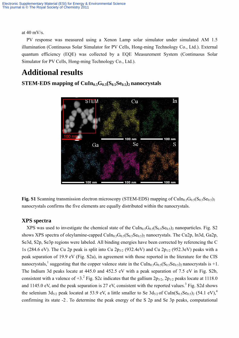
Additional results STEM-EDS mapping of CuIn0.5G0.5(S0.5Se0.5)2 nanocrystals
Fig. S1 Scanning transmission electron microscopy (STEM-EDS) mapping of CuIn0.5G0.5(S0.5Se0.5)2
nanocrystals confirms the five elements are equally distributed within the nanocrystals.
XPS spectra XPS was used to investigate the chemical state of the CuIn0.5G0.5(S0.5Se0.5)2 nanoparticles. Fig. S2
shows XPS spectra of oleylamine-capped CuIn0.5G0.5(S0.5Se0.5)2 nanocrystals. The Cu2p, In3d, Ga2p,
Se3d, S2p, Se3p regions were labeled. All binding energies have been corrected by referencing the C
1s (284.6 eV). The Cu 2p peak is split into Cu 2p3/2 (932.4eV) and Cu 2p1/2 (952.3eV) peaks with a
peak separation of 19.9 eV (Fig. S2a), in agreement with those reported in the literature for the CIS
nanocrystals,1 suggesting that the copper valence state in the CuIn0.5G0.5(S0.5Se0.5)2 nanocrystals is +1.
The Indium 3d peaks locate at 445.0 and 452.5 eV with a peak separation of 7.5 eV in Fig. S2b,
consistent with a valence of +3.2 Fig. S2c indicates that the gallium 2p3/2, 2p1/2 peaks locate at 1118.0
and 1145.0 eV, and the peak separation is 27 eV, consistent with the reported values.3 Fig. S2d shows
the selenium 3d5/2 peak located at 53.9 eV, a little smaller to Se 3d5/2 of CuIn(S0.5Se0.5)2 (54.1 eV),4
confirming its state -2 . To determine the peak energy of the S 2p and Se 3p peaks, computational
Electronic Supplementary Material (ESI) for Energy & Environmental ScienceThis journal is © The Royal Society of Chemistry 2011
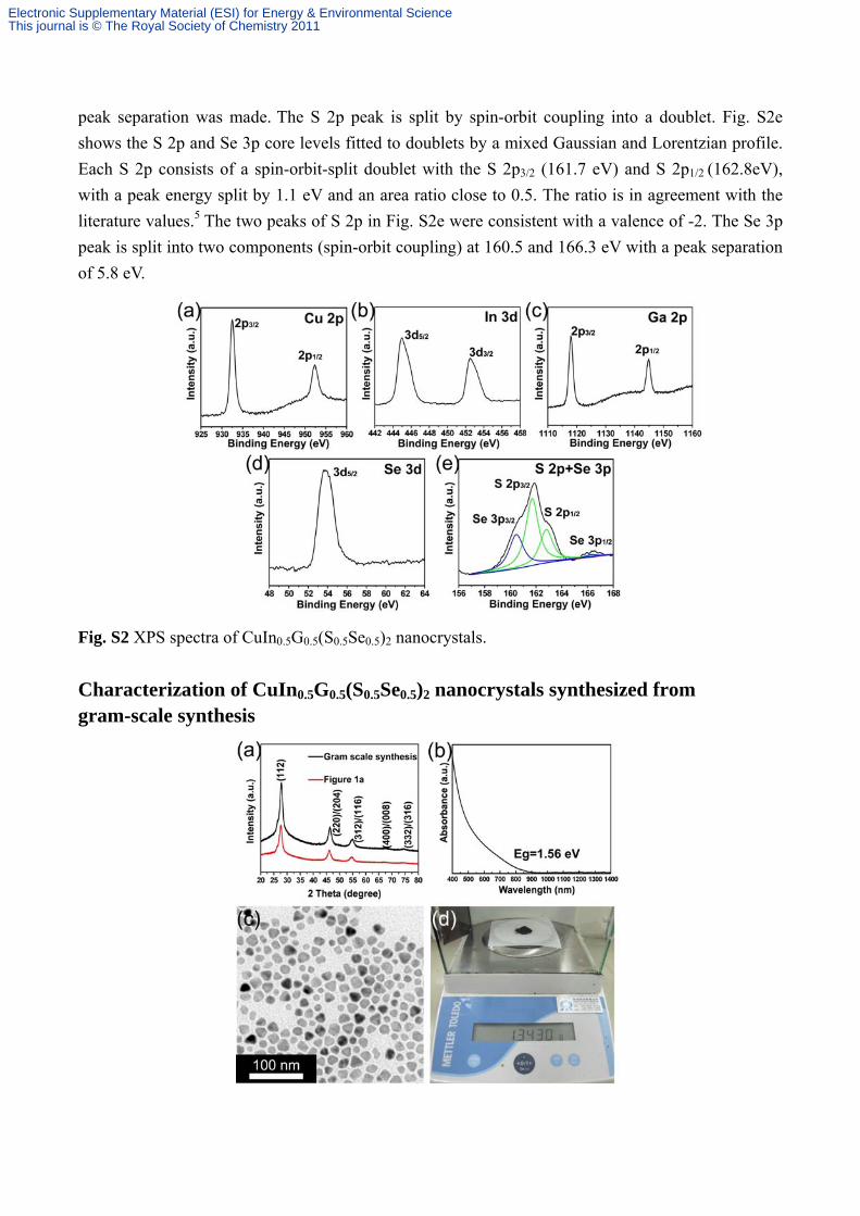
peak separation was made. The S 2p peak is split by spin-orbit coupling into a doublet. Fig. S2e
shows the S 2p and Se 3p core levels fitted to doublets by a mixed Gaussian and Lorentzian profile.
Each S 2p consists of a spin-orbit-split doublet with the S 2p3/2 (161.7 eV) and S 2p1/2 (162.8eV),
with a peak energy split by 1.1 eV and an area ratio close to 0.5. The ratio is in agreement with the
literature values.5 The two peaks of S 2p in Fig. S2e were consistent with a valence of -2. The Se 3p
peak is split into two components (spin-orbit coupling) at 160.5 and 166.3 eV with a peak separation
of 5.8 eV.
Fig. S2 XPS spectra of CuIn0.5G0.5(S0.5Se0.5)2 nanocrystals.
Characterization of CuIn0.5G0.5(S0.5Se0.5)2 nanocrystals synthesized from gram-scale synthesis
Electronic Supplementary Material (ESI) for Energy & Environmental ScienceThis journal is © The Royal Society of Chemistry 2011

Fig. S3 (a) XRD patterns of CuIn0.5G0.5(S0.5Se0.5)2 nanocrystals from 1.343 g CuIn0.5G0.5(S0.5Se0.5)2
nanocrystals, showing the same diffraction peaks with the normal scale (Fig. 1a) (b) UV-vis-NIR
absorption spectra of CuIn0.5G0.5(S0.5Se0.5)2 with a optical band gap of 1.56 eV (c) TEM images of
CuIn0.5G0.5(S0.5Se0.5)2 nanocrystals (d) Digital pictures of 1.343g CuIn0.5G0.5(S0.5Se0.5)2 nanocrystal.
Samples were collected after repeated purification procedures.
Lattice parameter analysis For many reports, the Cu–In–Se, Cu-Ga-S, and Cu–In–Ga–Se present a chalcopyrite structure
(tetragonal crystal system) belonging to space group I 4 2d.6-8 Chalcopyrite can be considered as a
superstructure of two zinc blende structures. The chalcopyrite (tetragonal) lattice is characterized by
lattice constants a and c. A corresponding formula in tetragonal crystal system is as shown in below.
2
2
2
22
2
1
c
l
a
kh
d
(S1)
where d is the d-spacing(interplanar distance), a and c represent the lengths of the unit cell edges; h,
k, and l are called crystallographic or Miller indices.
The formula illustrates dependence of the d-spacing on the Miller indices of the family and the
lengths of the three-unit cell edges. According to the Braggs’ law, the diffraction angle diffraction
angle (θhkl) of a reflection from a series of lattice planes (hkl) can be determined from the d-spacing
and the wavelength as follow equation:
hklhkl d2
sin
(S2)
The lattice parameters a and c can be easily calculated from the formulas. The lattice parameters (a
and c) versus composition plotted in Fig. S4.
In this system, the lattice constants are varied with the composition and showing that Vegard’s law
holds well for the lattice constant. According to Vegard’s law, the lattice pentanary alloyed
CuIn1-xGax(SySe1-y)2 nanocrystals can be express as :
a CuIn1-xGax(SySe1-y)2 =xyaCuGaS2 +x(1-y)aCuGaSe2
+(1-x)yaCuInS2+(1-x)(1-y)aCuInSe2 (S3)
c CuIn1-xGax(SySe1-y)2 =xycCuGaS2 +x(1-y)cCuGaSe2
+(1-x)ycCuInS2+(1-x)(1-y)cCuInSe2 (S4)
Electronic Supplementary Material (ESI) for Energy & Environmental ScienceThis journal is © The Royal Society of Chemistry 2011
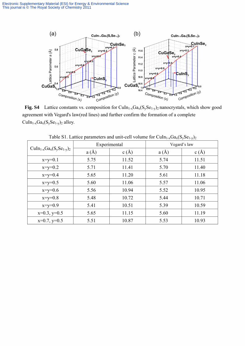
Fig. S4 Lattice constants vs. composition for CuIn1-xGax(SySe1-y)2 nanocrystals, which show good
agreement with Vegard's law(red lines) and further confirm the formation of a complete
CuIn1-xGax(SySe1-y)2 alloy.
Table S1. Lattice parameters and unit-cell volume for CuIn1-xGax(SySe1-y)2
CuIn1-xGax(SySe1-y)2 Experimental Vegard’s law
a (Å) c (Å) a (Å) c (Å)
x=y=0.1 5.75 11.52 5.74 11.51
x=y=0.2 5.71 11.41 5.70 11.40
x=y=0.4 5.65 11.20 5.61 11.18
x=y=0.5 5.60 11.06 5.57 11.06
x=y=0.6 5.56 10.94 5.52 10.95
x=y=0.8 5.48 10.72 5.44 10.71
x=y=0.9 5.41 10.51 5.39 10.59
x=0.3, y=0.5 5.65 11.15 5.60 11.19
x=0.7, y=0.5 5.51 10.87 5.53 10.93
Electronic Supplementary Material (ESI) for Energy & Environmental ScienceThis journal is © The Royal Society of Chemistry 2011

TEM and HRTEM images of CuIn1-xGax(SySe1-y)2 nanocrystals
Fig. S5 TEM images of CuIn1-xGax(SySe1-y)2 nanocrystals with (a) x=y=0.1, (b) x=y=0.2, (c) x=y=0.4,
(d) x=y=0.6, (e) x=y=0.8, and (f) x=y=0.9
Fig. S6 HRTEM images of CuIn1-xGax(SySe1-y)2 nanocrystals with (a) x=y=0.1, (b) x=y=0.2, (c)
x=y=0.4, (d) x=y=0.6, (e) x=y=0.8, and (f) x=y=0.9. The lattice spacings of (112) in each nanocrystal
increase gradually.
Electronic Supplementary Material (ESI) for Energy & Environmental ScienceThis journal is © The Royal Society of Chemistry 2011

Determination of optical band gap from UV-Vis-Near spectra: The direct allowed optical band gap Eg can be determined with the relation:9
n
gEhvDhv )( (S5)
where D is a constant, hν is the photon energy, and Eg is the optical band gap.
For a direct transition, n=1/2. By extrapolating the linear part of the plot to (αhν)2 = 0, values of the
direct band gap Eg for each composition x were determined.
The experimental values of (αhν)2 against hν is plotted in Fig. S7.
Fig. S7 Plot of (αhν)2 vs. (hν) for the CuIn1-xGax(SySe1-y)2 system
Electronic Supplementary Material (ESI) for Energy & Environmental ScienceThis journal is © The Royal Society of Chemistry 2011

Band gap profile approximation of CuIn1-xGax(SySe1-y)2 Band gap energy of CuIn1-xGax(SySe1-y)2 depending on 0≦x≦1 and on 0≦y≦1 may be
approximated from the binary models which yield an expression for Eg of the CuIn1-xGax(SySe1-y)2
alloy:
EgCIGSSe (x,y)= (1-y)[(1-x)Eg
CISSe (y)+x EgCGSSe(y)-bCIGSex(1-x)]
+y[(1-x)EgCISSe(y)+xEg
CGSSe(y)-bCIGSx(1-x)] (1)
Eg
CISSe(y)=yEgCuInS2+(1-y)Eg
CuInSe2-bCISSey(1-y) (S6)
EgCGSSe(y)=yEg
CuGaS2+(1-y)EgCuGaSe2-bCGSSey(1-y) (S7)
EgCIGS (x)=xEg
CuGaS2+(1-x)EgCuInS2-bCIGSx(1-x) (S8)
EgCIGSe(x)=xEg
CuGaSe2+(1-x)EgCuInSe2-bCIGSex(1-x) (S9)
Applying the corresponding band gap values for CuInS2, 4 CuInSe2 (Fig. 11a), CuGaS2 (Fig. 11b),
CuGaSe210 (Table S2) and the optical bowing constants of CISSe, 4 CGSSe, 11 CIGS, 11 CIGSe12
(Table S3), the equation can be simplified to the following expression:
EgCIGSSe(x,y)=(0.98+0.167x2+0.17y2+0.023x2y-0.17xy2+0.397xy+0.31y+0.523x) eV (2)
This equation was typed into Matlab and the result is shown in Fig. 4.
Table S2. Band gap energies of ternary chalcopyrites
CuIn1-xGax(SySe1-y)2 alloy Eg (eV)
x=0, y=0 : CuInSe2 0.98
x=0, y=1 : CuInS2 1.46
x=1, y=0 : CuGaSe2 1.67
x=1, y=1 : CuGaS2 2.4
Table S3. Optical bowing constants b for the quaternary chalcopyrites CuIn1-xGax(SySe1-y)2 alloy b (eV)
x=0, 0≦y≦1 : CuIn(SySe1-y)2 (CISSe) 0.17
x=1, 0≦y≦1 : CuGa(SySe1-y)2 (CGSSe) 0
0≦x≦1, y=1 : Cu(In1-xGax)S2 (CIGS) 0.19
0≦x≦1, y=0 : Cu(In1-xGax)Se2 (CIGSe) 0.167
Electronic Supplementary Material (ESI) for Energy & Environmental ScienceThis journal is © The Royal Society of Chemistry 2011

Cyclic voltammetry analysis:
Cyclic voltammetry (CV) is a dynamic electrochemical method to measure the band-edge
positions of nanomaterials.13 From CV spectra, the band-edge positions (i.e., the highest occupied
molecular orbital (HOMO) and lowest unoccupied molecular orbital (LUMO) energy position) can
be determined. Oxidation potential was correlated directly with the ionization potential(Ip) and the
reduction potential with the electron affinity(Ea), the band edge positions of electroactive materials
can be calculated.14 The HOMO and LUMO energy levels can be derived from the onset oxidation
potential (Eox) and onset reduction potential (Ered), respectively, according to equation below:13
EHOMO=-Ip=-(Eox+4.71) eV (S10)
ELUMO=-Ea=-(Ered+4.71) eV (S11)
where the onset of the potential values are relative to a Ag/Ag+ reference electrode. The value of 4.71
represents the difference between the vacuum level potential of the normal hydrogen electrode (NHE)
and the potential of the Ag/AgCl electrode versus NHE. We started from zero and the
scanning voltage ranges was from -2.5 to 2.5 V. Fig. S8 outlines the onset potentials for the oxidation
and reduction of our nanocrystals.
Electronic Supplementary Material (ESI) for Energy & Environmental ScienceThis journal is © The Royal Society of Chemistry 2011
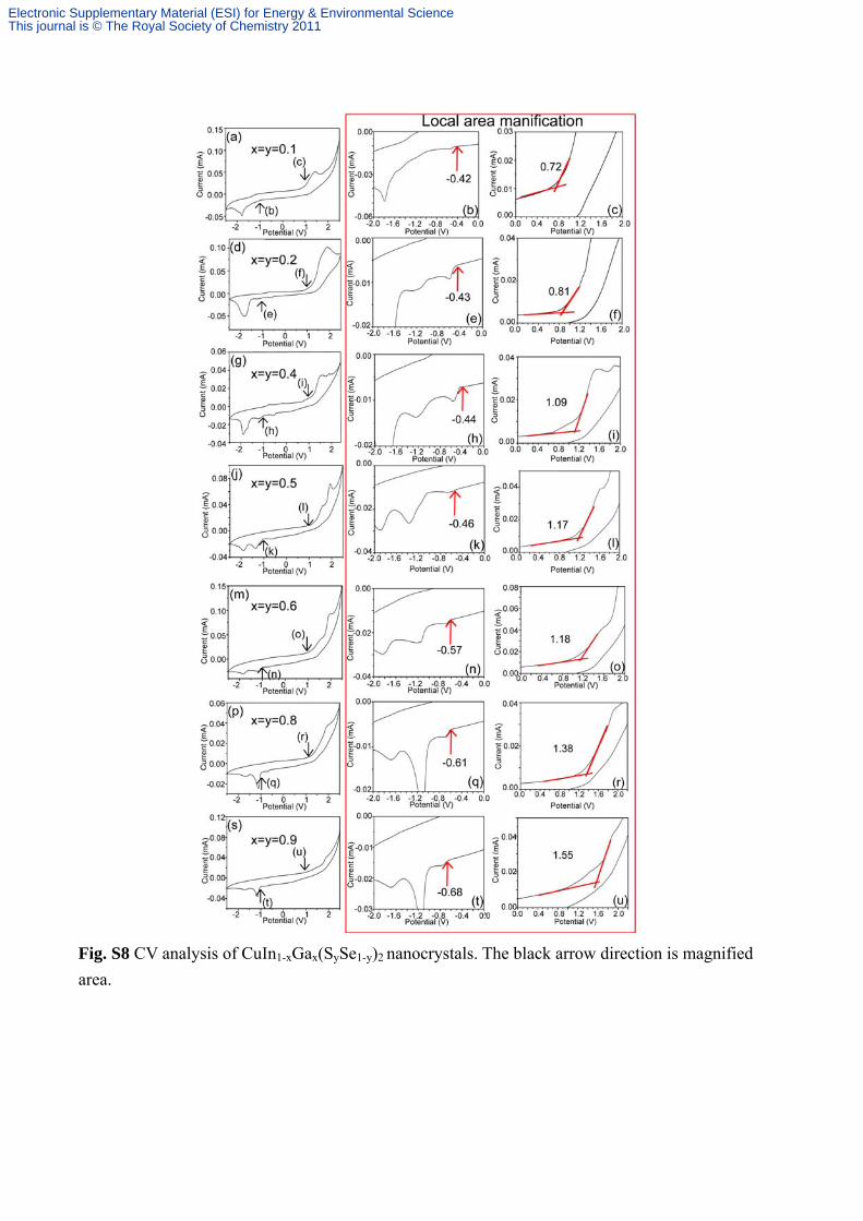
Fig. S8 CV analysis of CuIn1-xGax(SySe1-y)2 nanocrystals. The black arrow direction is magnified
area.
Electronic Supplementary Material (ESI) for Energy & Environmental ScienceThis journal is © The Royal Society of Chemistry 2011

Table S4. Composition, Band Gap Energies of CuIn1-xGax(SySe1-y)2 Nanocrystals determined by
absorption spectra, CV, and Eq. (2)
Target compound Precursor composition Composition measured by EDS Eg (eV) Eg (eV) Eg (eV)
CuIn1‐xGax(SySe1‐y)2 (Cu/In/Ga/S/Se atom ratio %) (Cu/In/Ga/S/Se atom ratio %) determined by
absorption spectra
determined by
CV
determined by
Eq. (2)
CuIn0.9Ga0.1(S0.1Se0.9)2 25 : 22.5 : 2.5 : 5 : 45 24.11 : 22.04 : 2.84 : 5.69 : 45.32 1.08 1.14 1.07
(1 : 0.9 : 0.1 : 0.2 : 1.8) (0.97 : 0.88 : 0.11 : 0.22 : 1.82)
CuIn0.8Ga0.2(S0.2Se0.8)2 25 : 20 : 5 : 10 : 40 24.5 : 19.64 : 5.73 : 10.21 : 39.91 1.17 1.24 1.17
(1 : 0.8 : 0.2 : 0.4 : 1.6) (0.98 : 0.79 : 0.23 : 0.4 : 1.6)
CuIn0.6Ga0.4(S0.4Se0.6)2 25 : 15 : 10 : 20 : 30 26.79 : 15.01 : 9.89 : 17.85 : 30.46 1.42 1.53 1.42
(1 : 0.6 : 0.4 : 0.8 : 1.2) (1.07 : 0.6 : 0.4 : 0.71 : 1.22)
CuIn0.5Ga0.5(S0.5Se0.5)2 25 : 12.5 : 12.5 : 25 : 25 25.12 : 12.44 : 12.42 : 24.86 : 25.16 1.56 1.63 1.56
(1 : 0.5 : 0.5 : 1.0 : 1.0) (1 : 0.5 : 0.5 : 0.99 : 1.01)
CuIn0.4Ga0.6(S0.6Se0.4)2 25 : 10 : 15 : 30 : 20 24.08 : 9.32 : 15 : 30.85 : 20.75 1.71 1.75 1.71
(1 : 0.4 : 0.6 : 1.2 : 0.8) (0.96 : 0.37 : 0.6 : 1.23 : 0.83)
CuIn0.2Ga0.8(S0.8Se0.2)2 25 : 5 : 20 : 40 : 10 25.45 : 4.3 : 20.92 : 37.92 : 11.41 2.01 1.99 2.04
(1 : 0.2 : 0.8 : 1.6 : 0.4) (1.01 : 0.17 : 0.84 : 1.52 : 0.46)
CuIn0.1Ga0.9(S0.9Se0.1)2 25 : 2.5 : 22.5 : 45 : 5 24.18 : 3.11 : 22.43 : 43.44 : 6.84 2.20 2.23 2.22
(1 : 0.1 : 0.9 : 1.8 : 0.2) (0.97 : 0.12 : 0.9 : 1.74 : 0.27)
Electronic Supplementary Material (ESI) for Energy & Environmental ScienceThis journal is © The Royal Society of Chemistry 2011
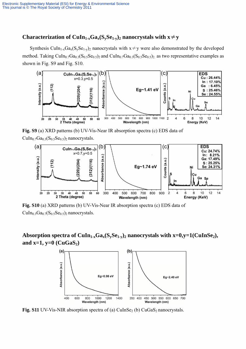
Characterization of CuIn1-xGax(SySe1-y)2 nanocrystals with x≠y
Synthesis CuIn1-xGax(SySe1-y)2 nanocrystals with x≠y were also demonstrated by the developed
method. Taking CuIn0.7Ga0.3(S0.5Se0.5)2 and CuIn0.7Ga0.3(S0.5Se0.5)2. as two representative examples as
shown in Fig. S9 and Fig. S10.
Fig. S9 (a) XRD patterns (b) UV-Vis-Near IR absorption spectra (c) EDS data of
CuIn0.7Ga0.3(S0.5Se0.5)2 nanocrystals.
Fig. S10 (a) XRD patterns (b) UV-Vis-Near IR absorption spectra (c) EDS data of
CuIn0.3Ga0.7(S0.5Se0.5)2 nanocrystals.
Absorption spectra of CuIn1-xGax(SySe1-y)2 nanocrystals with x=0,y=1(CuInSe2), and x=1, y=0 (CuGaS2)
Fig. S11 UV-Vis-NIR absorption spectra of (a) CuInSe2 (b) CuGaS2 nanocrystals.
Electronic Supplementary Material (ESI) for Energy & Environmental ScienceThis journal is © The Royal Society of Chemistry 2011

Fig. S12. FTIR pattern of CuIn0.5Ga0.5(S0.5Se0.5)2 nanocrystal film (red line) and oleylamine (black
line).
REFERENCES
1 F. M. Courtel, R. W. Paynter, B. t. Marsan and M. Morin, Chem. Mat., 2009, 21, 3752-3762.
2 D. Pan, X. Wang, Z. H. Zhou, W. Chen, C. Xu and Y. Lu, Chem. Mat., 2009, 21, 2489-2493.
3 In Handbook of x-ray photoelectron spectroscopy, ed. J. F. Moulder, W. F. Stickle, P. E. Sobol
and K. D. Bomben, Physical Electronics, 1992.
4 M.-Y. Chiang, S.-H. Chang, C.-Y. Chen, F.-W. Yuan and H.-Y. Tuan, The Journal of Physical
Chemistry C, 2011, 115, 1592-1599.
5 B. Canava, J. Vigneron, A. Etcheberry, D. Guimard, P. P. Grand, J. F. Guillemoles, D. Lincot,
S. Ould Saad Hamatly, Z. Djebbour and D. Mencaraglia, Thin Solid Films, 2003, 431-432,
289-295.
6 D. K. Suri, K. C. Nagpal and G. K. Chadha, J. Appl. Crystallogr., 1989, 22, 578-583.
7 M. Souilah, A. Lafond, N. Barreau, C. Guillot-Deudon and J. Kessler, Appl. Phys. Lett., 2008,
92, 241923.
8 M. Souilah, X. Rocquefelte, A. Lafond, C. Guillot-Deudon, J. P. Morniroli and J. Kessler,
Thin Solid Films, 2009, 517, 2145-2148.
9 S. T. Tan, B. J. Chen, X. W. Sun, W. J. Fan, H. S. Kwok, X. H. Zhang and S. J. Chua, J. Appl.
Phys., 2005, 98, 013505.
10 R. Noufi, R. Powell, C. Herrington and T. Coutts, Solar Cells, 1986, 17, 303-307.
11 S. H. Wei and A. Zunger, J. Appl. Phys., 1995, 78, 3846-3856.
12 (a) In Handbook of photovoltaic science and engineering,ed. A. Luque, S. Hegedus, Wiley,
2003; (b) F. Kang, J. P. Ao, G. Z. Sun, Q. He and Y. Sun, Semicond. Sci. Technol., 2009,
24,075015.
13 H. Zhong, S. S. Lo, T. Mirkovic, Y. Li, Y. Ding, Y. Li and G. D. Scholes, ACS Nano, 2010, 4,
Electronic Supplementary Material (ESI) for Energy & Environmental ScienceThis journal is © The Royal Society of Chemistry 2011

5253-5262.
14 E. Kucur, J. Riegler, G. A. Urban and T. Nann, J. Chem. Phys., 2003, 119, 2333-2337.
Electronic Supplementary Material (ESI) for Energy & Environmental ScienceThis journal is © The Royal Society of Chemistry 2011