chemistry and structure of ru/sio2 and ru/al2o3 interfaces
TRANSCRIPT
University of Central Florida University of Central Florida
STARS STARS
Electronic Theses and Dissertations
2019
Chemistry and Structure of Ru/SiO2 and Ru/Al2O3 Interfaces Chemistry and Structure of Ru/SiO2 and Ru/Al2O3 Interfaces
Sameer Ezzat University of Central Florida
Part of the Chemistry Commons
Find similar works at: https://stars.library.ucf.edu/etd
University of Central Florida Libraries http://library.ucf.edu
This Doctoral Dissertation (Open Access) is brought to you for free and open access by STARS. It has been accepted
for inclusion in Electronic Theses and Dissertations by an authorized administrator of STARS. For more information,
please contact [email protected].
STARS Citation STARS Citation Ezzat, Sameer, "Chemistry and Structure of Ru/SiO2 and Ru/Al2O3 Interfaces" (2019). Electronic Theses and Dissertations. 6388. https://stars.library.ucf.edu/etd/6388
CHEMISTRY AND STRUCTURE OF Ru/SiO2 AND Ru/ Al2O3 INTERFACES
by
SAMEER SA’ADALLAH EZZAT
B.C. University of Mosul, 1998
M.Sc. University of Mosul, 2000
A dissertation submitted in partial fulfillment of the requirements
for the degree of Doctor of Philosophy
in the Department of Chemistry
in the College of Science
at the University of Central Florida
Orlando, Florida
Spring Term
2019
Major Professor: Andres Campiglia, Kevin R. Coffey

ii
© 2019 SAMEER SA’ADALLAH EZZAT

iii
ABSTRACT
The resistivity size effect in nanoscale metals is of both scientific and technological
interest, the latter due to its importance to interconnects between transistors in integrated circuits.
In this work we report the variation of resistivity associated with surface scattering of ex-situ
annealed single crystal Ru thin films grown on sapphire substrates by sputter deposition. A set of
samples were overcoated with dielectric and subjected to a variety of reducing and oxidizing
anneals. The changes in the chemistry and structure of the dielectric interface induced by the
anneals, as determined by x-ray reflectivity and x-ray photoelectron spectroscopy measurements,
are related to the changes in the specularity of the surface for electron scattering in the context of
the Fuchs-Sondheimer semi-classical model of the resistivity size effect.
iv
This dissertation is dedicated to my father (1939-2005), my mother, and my wife. They have been
a constant source of support and encouragement during the challenges of doctoral study and I am
really thankful for having them in my life.
My lovely kids
Ibrahim, Estabraq, and Razan
For inspiring me to not give up.
My brothers and sister
For their love, endless support and encouragement.
v
ACKNOWLEDGMENTS
It is a milestone that would have not been possible without the continuous support and
guidance of my research advisor, Professor Kevin R. Coffey, and my academic advisor, Professor
Dr. Andres D. Campiglia. Their continuous and enormous support during my Ph.D. research with
their patience, enthusiasm, and immense knowledge was greatly appreciated. Their guidance
helped me through the duration of my Ph.D. experience and preparation of this dissertation.
I extend my thanks to the dissertation committee members Dr. James Harper, Dr. Shengli
Zou, and Dr. Andrew Frazer.
I would like to thank the Iraqi government and Ministry of Higher Education and Scientific
Research for providing this opportunity and their continuous support.
Edward Dein and Dr. Prabhu Doss Mani are important people, they had helped me in my
research learning everything in clean room right from sputtering tools to lithography process.
I would like to thank Dr. William Kaden and Asim Khaniya for all help.
Special thanks to my brothers and sister, and do not forget my friends during my PhD
studies.
My colleagues of Dr. Coffey’s group
My sincere thanks to Kirk Scammon, Karen Glidewell, Mikhail Klimov, and Dr. Mike
Hawkridge for assistance with characterization facilities
vi
TABLE OF CONTENTS
ABSTRACT ................................................................................................................................... iii
ACKNOWLEDGMENTS .............................................................................................................. v
TABLE OF CONTENTS ............................................................................................................... vi
LIST OF FIGURES ....................................................................................................................... ix
LIST OF TABLES ....................................................................................................................... xiii
CHAPTER 1 INTRODUCTION .................................................................................................... 1
1.1 Ruthenium ........................................................................................................................ 1
1.2 Ruthenium oxidation ........................................................................................................ 3
1.3 Reduction of RuO2 (110) on Ru (0001) surface ............................................................... 8
1.3.1 Reduction by hydrogen ............................................................................................. 8
1.3.2 Reduction by carbon monoxide ................................................................................ 9
1.3.3 Reduction by methanol ........................................................................................... 10
CHAPTER 2 BACKGROUND AND MOTIVATION ................................................................ 11
2.1 Resistivity of thin metal films ........................................................................................ 11
2.2 Adsorbate induced changes in resistivity of atomically clean metal films .................... 12
2.2.1 Suhrmann model ..................................................................................................... 13
2.2.2 Sachtler model ........................................................................................................ 15
2.2.3 Fuchs-Sondheimer model ....................................................................................... 15
2.2.4 The scattering hypothesis ........................................................................................ 16
2.3 Resistivity due to variation of metal film thickness ....................................................... 19
CHAPTER 3 EXPERIMENTAL .................................................................................................. 24
3.1 Introduction .................................................................................................................... 24
3.2 Sputter deposition ........................................................................................................... 24
3.3 XRD and XRR characterization ..................................................................................... 27
3.3.1 XRD characterization .............................................................................................. 27
3.3.2 XRR characterization .............................................................................................. 27
3.4 Four-Point Resistivity Measurement .............................................................................. 28
3.5 Sample preparation details ............................................................................................. 30
3.5.1 Ru single crystal film deposition ............................................................................ 30
3.5.2 Anneal to 700C ...................................................................................................... 32
vii
3.5.3 Step anneal to 950C ............................................................................................... 34
3.5.4 Additional anneals for series 3 ................................................................................ 34
3.5.5 SiO2 overlayer depositions ...................................................................................... 35
3.5.6 Al2O3 overlayer depositions .................................................................................... 36
3.5.7 Additional anneals for series 5 ................................................................................ 36
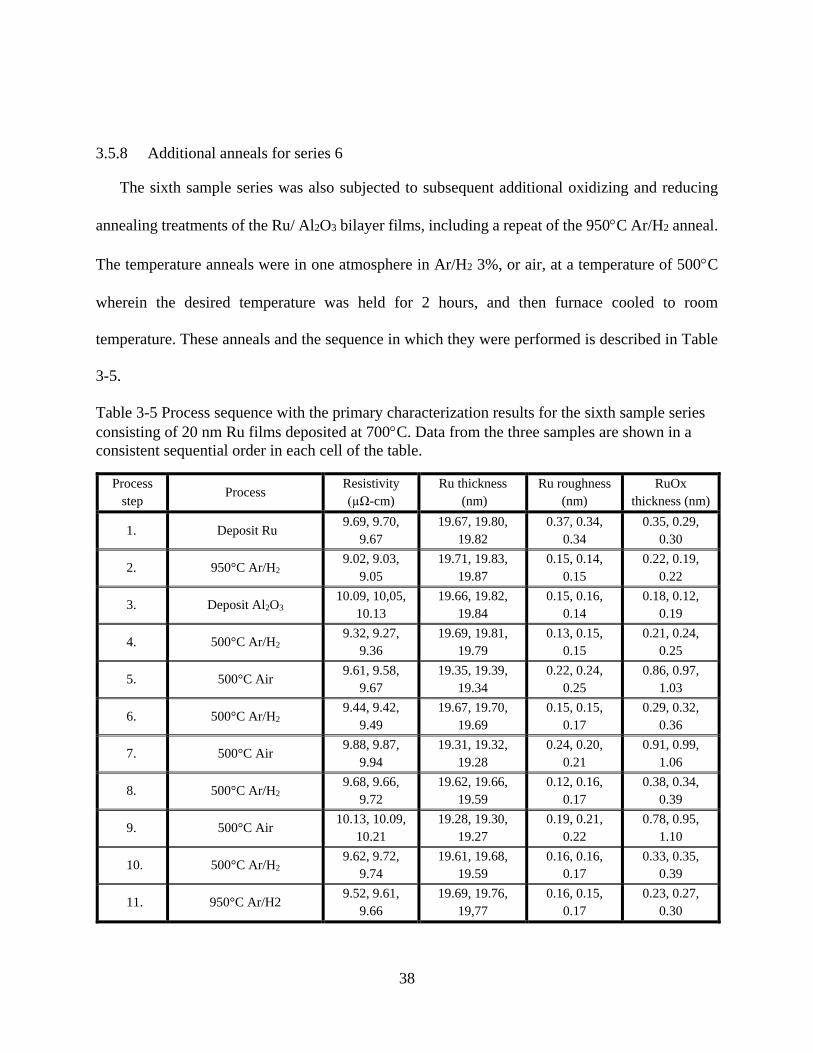
3.5.8 Additional anneals for series 6 ................................................................................ 38
CHAPTER 4 SINGLE CRYSTAL RUTHENIUM FILMS ......................................................... 39
4.1 X-ray diffraction ............................................................................................................. 39
4.2 X-ray reflectivity ............................................................................................................ 41
4.3 Roughness sample series one ......................................................................................... 42
4.4 Modelling ....................................................................................................................... 43
4.5 Resistivity ....................................................................................................................... 44
4.5.1 Resistivity sample series 1 ...................................................................................... 44
4.5.2 Resistivity sample series 2 and 3 ............................................................................ 45
4.5.3 Sample series 3 ....................................................................................................... 47
4.6 LEED characterization ................................................................................................... 48
4.7 XPS characterization Ru ................................................................................................ 50
CHAPTER 5 Ru/SiO2 and Ru/Al2O3 INTERFACE ..................................................................... 54
5.1 XRR layer thickness ....................................................................................................... 54
5.2 XPS characterization Ru/SiO2 ........................................................................................ 55
5.3 LEED of Ru/SiO2 and Ru/Al2O3 .................................................................................... 58
5.4 Resistivity and specularity ............................................................................................. 59
5.4.1 Sample series 4 - evaporated SiO2 on Ru 20 nm films ........................................... 59
5.4.2 Sample series 5 - sputtered SiO2 on Ru 20 nm films .............................................. 60
5.4.3 Samples series 6 - Sputtered Al2O3 on Ru 20 nm films .......................................... 65
CHAPTER 6 RUTHENIUM ON (1120), (1010), (1012), and (1014) SAPPHIRE .................... 68
6.1 Introduction .................................................................................................................... 68
6.2 Ru on sapphire (1120) .................................................................................................... 69
6.3 Ru on sapphire (1010) .................................................................................................... 73
6.4 Ru on sapphire (1012) .................................................................................................... 75
6.5 Ru on sapphire (1014) .................................................................................................... 76
6.6 Conclusion ...................................................................................................................... 78
viii
CHAPTER 7 SUMMARY ............................................................................................................ 79
CHAPTER 8 CHAPTER 8 FUTURE WORK ............................................................................. 81
8.1 Deposit Ru thin film on sapphire (1120) and sapphire (1010) ...................................... 81
8.2 Ru (0001)/Metal oxide interfaces ................................................................................... 81
8.3 The effect of annealing temperature ............................................................................... 82
LIST OF REFERENCES .............................................................................................................. 83

ix
LIST OF FIGURES
Figure 1-1 The hcp crystal structure with ABA stacking. .............................................................. 1
Figure 1-2 The hcp crystal structure, (a) identifies the basal plane as the (0001) plane and is the
plane containing the darkened circles. Figure 1.2 (a) also identifies the [0001] direction by the
arrow that is perpendicular to the (0001) plane. Figure 1.2 (b) similarly identifies the (1120)
plane and [1120] direction while Figure 1.2 (c) identifies an (1010) plane and [1010] direction . 2
Figure 1-3 STM images show the chemisorbed oxygen on Ru (0001) .......................................... 5
Figure 1-4 Calculated free energy O-Ru (0001) structures ............................................................ 6
Figure 1-5 The RuO2 (110) and RuO2 (100) on Ru (0001) substrate. ............................................ 7
Figure 1-6 Surface X-ray diffraction explain the reduction of RuO2 on Ru (0001) surface via H2
molecules at various temperatures. ................................................................................................. 9
Figure 2-1 Resistivity increased due to gas adsorption on a thin film conductor ........................ 13
Figure 2-2 Four theories that have been proposed to understand the resistivity change due to
molecules or atoms absorbing on the surface of a thin film. ........................................................ 14
Figure 2-3 The resistivity effect of O2, CO, and C2H4 adsorption on Ag thin films ................... 17
Figure 2-4 Various adsorbates on Ru (0001) ............................................................................... 18
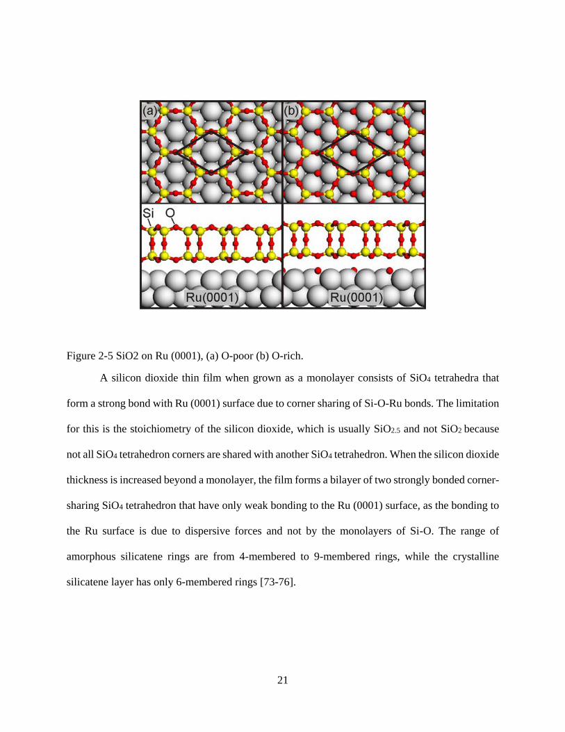
Figure 2-5 SiO2 on Ru (0001), (a) O-poor (b) O-rich .................................................................. 21
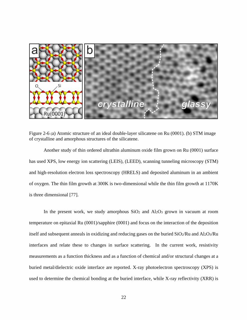
Figure 2-6 (a) Atomic structure of an ideal double-layer silicatene on Ru (0001). (b) STM image
of crystalline and amorphous structures of the silicatene. ............................................................ 22
Figure 3-1 Geometry of sputtering deposition .............................................................................. 26
x
Figure 3-2 Representative XRR data from a 4.6nm thick SiO2 on a 20.8nm-thick Ru (0001) layer.
(a) upper (black) curve is for measured data shifted by a factor of 101 for clarity and (b) the
lower (red) curve is for fitted mpdel. ............................................................................................ 28
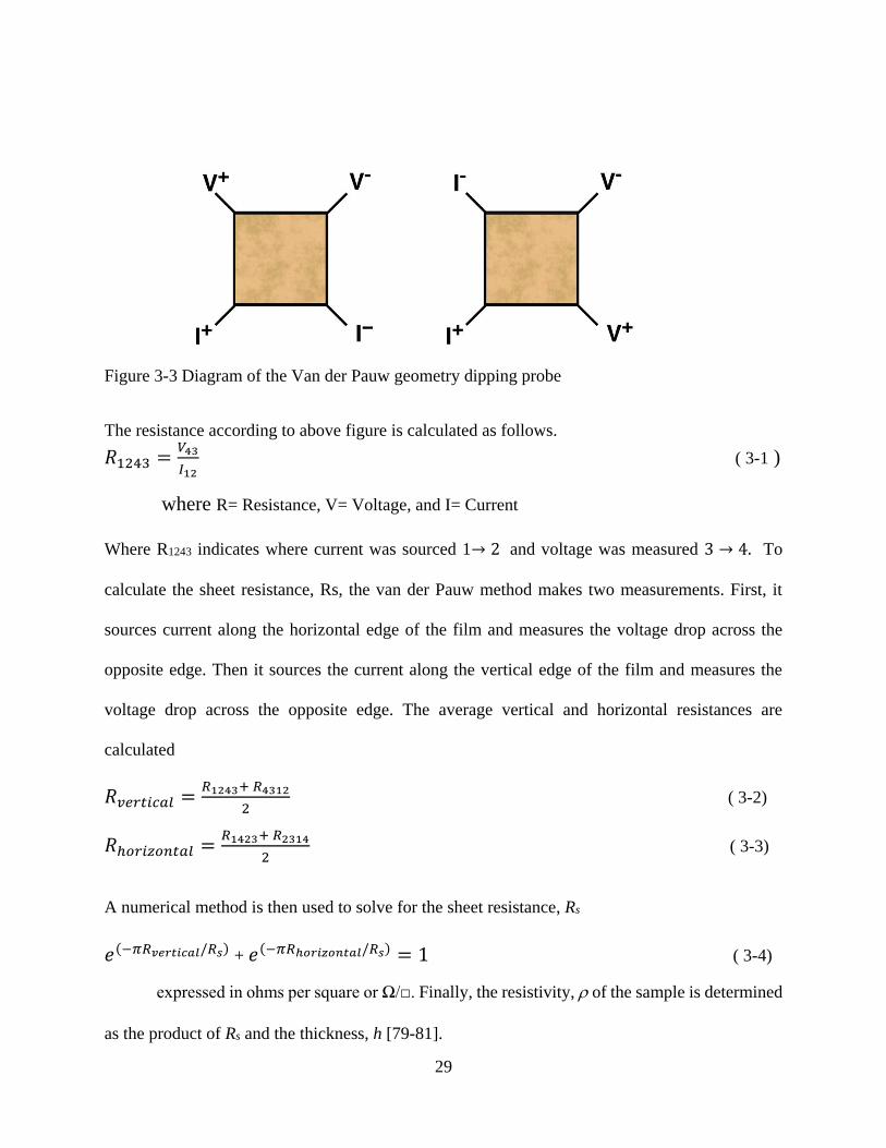
Figure 3-3 Diagram of the Van der Pauw geometry dipping probe ............................................. 29
Figure 4-1 The diagram of (a) theta-2theta scan and (b) phi scan ................................................ 39
Figure 4-2 Specular XRD scan for a Ru film on sapphire (0001) deposited at 700ºC with
thickness d = 39.8 nm ................................................................................................................... 40
Figure 4-3 XRD scan of the Ru 1122 peaks overlaid with a scan of the sapphire 1126
peaks ............................................................................................................................................. 41
Figure 4-4 XRR data from 40 nm-thick Ru (0001) layer deposited at 400C. (a) upper (red) curve
is Ru after annealed and shifted by a factor of 10 for clarity and (b) the lower (blue) curve is Ru
before as deposited. ....................................................................................................................... 42
Figure 4-5 Ru roughness of Ru thin films, as deposited and after annealed. ............................... 43
Figure 4-6 Resistivity of Ru thin films as deposited and after annealed at 700C. ...................... 45
Figure 4-7 Resistivity versus thickness for c-axis single crystal Ru films deposited at 350C
(circles) and 700C (squares) and ex-situ step-annealed to 950C in Ar/H2 3%. The solid line is
the calculation of the FS model. ................................................................................................... 46
Figure 4-8 Resistivity of Ru 20 nm thin film during the annealing process ................................. 47
Figure 4-9 LEED images at 68 eV for an air exposed Ru film (a) after deposition at 350C, (b)
after deposition at 700C, (c) after deposition at 700C and ex-situ annealing to 950C in
Ar/3%H2, and (d) a sample Ar ion beam cleaned and annealed to 1,000C in UHV conditions
with an H2 background. ................................................................................................................. 48
xi
Figure 4-10 Represents a series of XPS spectra of Ru 3d peak collected from samples annealing
in two different environments, Ar/H2 and air, alternatively. Samples A and C are after annealed
in Ar/H2 (3%) atmosphere where samples B and D after annealed in air at 300C. ...................... 52
Figure 5-1 XRR data from a 4.6nm thick SiO2 on a 20.8nm-thick Ru (0001) layer. (a) upper
(black) curve is for measured data shifted by a factor of 10 for clarity and (b) the lower (red)
curve is the model prediction. ....................................................................................................... 55
Figure 5-2 XPS data for Ru 3d (a), Si 2p (b), and O 1s (c) for the same sample following the 2nd
(blue) 4th (green), and 5th (red) stage in the annealing process described in Table 3-2. Ru0 and
Ruδ+ in figure 5-2(a) correspond to metallic ruthenium and ruthenium oxide (RuO2) respectively.
....................................................................................................................................................... 56
Figure 5-3 LEED images at 68 eV for an air exposed (a) Ru/SiO2 and (b) Ru/Al2O3 .................. 58
Figure 5-4 Resistivity and calculated upper surface specularity for the FS model as a function of
evaporated SiO2 thickness for 20 nm thick Ru samples. .............................................................. 60
Figure 5-5 Film resistivity and FS model upper surface specularity (pu) as a function of sample
processing. Shown are average values for the five samples with error bars to reflect the extreme
values amongst the five. ................................................................................................................ 61
Figure 5-6 Shows (a) Ru metal thickness change, (b) RuOx, (c) Ru oxide to Ru metal ratio, (d)
Ru roughness and (e) surface specularity (p) processing as a function of sample shown are
average values for the five samples with error bars to reflect the extreme values amongst the five.
....................................................................................................................................................... 63
Figure 5-7 The comparison between the XRR of RuOx layer and the XPS Ru+/Ru0 ratio ........... 64

xii
Figure 5-8 Film resistivity, RuOx, Ru metal thickness, and roughness as a function of sample
processing. Shown are average values for the three samples with error bars to reflect the extreme
values amongst the three. .............................................................................................................. 66
Figure 6-1 XRD for a Ru film on sapphire (1120) deposited at 500ºC with thickness d = 39.7 nm
....................................................................................................................................................... 69
Figure 6-2 The scan of Ru thin film on sapphire (1120) ........................................................... 70
Figure 6-3 The scan of sapphire (1120) ..................................................................................... 71
Figure 6-4 The resistivity of Ru 40 nm on sapphire (1120) ......................................................... 72
Figure 6-5 The 2 scan of Ru thin film on sapphire (1010). ........................................................ 73
Figure 6-6 The resistivity of Ru 40 nm on sapphire (1010) ......................................................... 74
Figure 6-7 The 2 scan of Ru thin film on sapphire (1012) ......................................................... 75
Figure 6-8 The resistivity of Ru 40 nm on sapphire (1012) ......................................................... 76
Figure 6-9 The 2 scan of Ru thin film on sapphire (1014) ......................................................... 77
Figure 6-10 The resistivity of Ru 40 nm on sapphire (1014) ....................................................... 78
xiii
LIST OF TABLES
Table 1-1 Oxygen affinity of metals expressed as the required O2 vapor pressure (PO2) for the
oxide to be in thermodynamic equilibrium with the metal at 1000K. ............................................ 3
Table 3-1 Listing of sample series studied. .................................................................................. 31
Table 3-2 Thickness, roughness, and resistivity of Ru 10-80 nm that deposited at different
temperature and annealed at 700C in one atmosphere of flowing Ar/H2 3% ............................. 33
Table 3-3 Process sequence with the primary characterization results for the third sample series
consisting of 20 nm Ru films deposited at 700C. ....................................................................... 35
Table 3-4 Process sequence with the primary characterization results for the fifth sample series
consisting of 20 nm Ru films deposited at 700C. Data from the five samples are shown in a
consistent sequential order in each cell of the table, except for the Ru+/Ru0 ratios determined
from XPS where only the same two of the five samples were characterized. .............................. 37
Table 3-5 Process sequence with the primary characterization results for the sixth sample series
consisting of 20 nm Ru films deposited at 700C. Data from the three samples are shown in a
consistent sequential order in each cell of the table. ..................................................................... 38
Table 4-1 Listing of FS model parameters ................................................................................... 50
Table 6-1 The thickness, roughness, and resistivity of Ru 40 nm thin films on sapphire (1120). 71
Table 6-2 The thickness, roughness, and resistivity of Ru 40 nm thin films on sapphire (1010). 74
Table 6-3 The thickness, roughness, and resistivity of the Ru 40 nm thin films on sapphire
(1012). ........................................................................................................................................... 76
Table 6-4 The thickness, roughness, and resistivity of Ru 40 nm thin films on sapphire (1014). 77
1
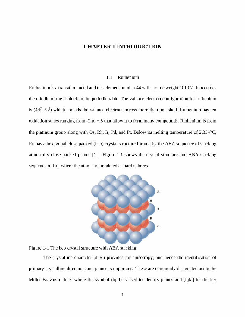
CHAPTER 1 INTRODUCTION
1.1 Ruthenium
Ruthenium is a transition metal and it is element number 44 with atomic weight 101.07. It occupies
the middle of the d-block in the periodic table. The valence electron configuration for ruthenium
is (4d7, 5s1) which spreads the valance electrons across more than one shell. Ruthenium has ten
oxidation states ranging from -2 to + 8 that allow it to form many compounds. Ruthenium is from
the platinum group along with Os, Rh, Ir, Pd, and Pt. Below its melting temperature of 2,334C,
Ru has a hexagonal close packed (hcp) crystal structure formed by the ABA sequence of stacking
atomically close-packed planes [1]. Figure 1.1 shows the crystal structure and ABA stacking
sequence of Ru, where the atoms are modeled as hard spheres.
Figure 1-1 The hcp crystal structure with ABA stacking.
The crystalline character of Ru provides for anisotropy, and hence the identification of
primary crystalline directions and planes is important. These are commonly designated using the
Miller-Bravais indices where the symbol (hjkl) is used to identify planes and [hjkl] to identify
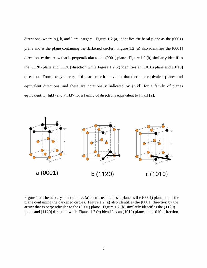
2
directions, where h,j, k, and l are integers. Figure 1.2 (a) identifies the basal plane as the (0001)
plane and is the plane containing the darkened circles. Figure 1.2 (a) also identifies the [0001]
direction by the arrow that is perpendicular to the (0001) plane. Figure 1.2 (b) similarly identifies
the (1120) plane and [1120] direction while Figure 1.2 (c) identifies an (1010) plane and [1010]
direction. From the symmetry of the structure it is evident that there are equivalent planes and
equivalent directions, and these are notationally indicated by hjkl for a family of planes
equivalent to (hjkl) and <hjkl> for a family of directions equivalent to [hjkl] [2].
Figure 1-2 The hcp crystal structure, (a) identifies the basal plane as the (0001) plane and is the
plane containing the darkened circles. Figure 1.2 (a) also identifies the [0001] direction by the
arrow that is perpendicular to the (0001) plane. Figure 1.2 (b) similarly identifies the (1120)
plane and [1120] direction while Figure 1.2 (c) identifies an (1010) plane and [1010] direction.
3
1.2 Ruthenium oxidation
Ru is inert to most chemicals over a broad range of temperatures. It is a near-noble metal,
having an oxygen affinity greater than Au, Ag, Pt and Pd, but less than that of Cu, Pb, Ni, and Si.
For example, Ru metal will not readily oxidize in air at room temperature, but easily forms RuO2
above 800K [3-4].
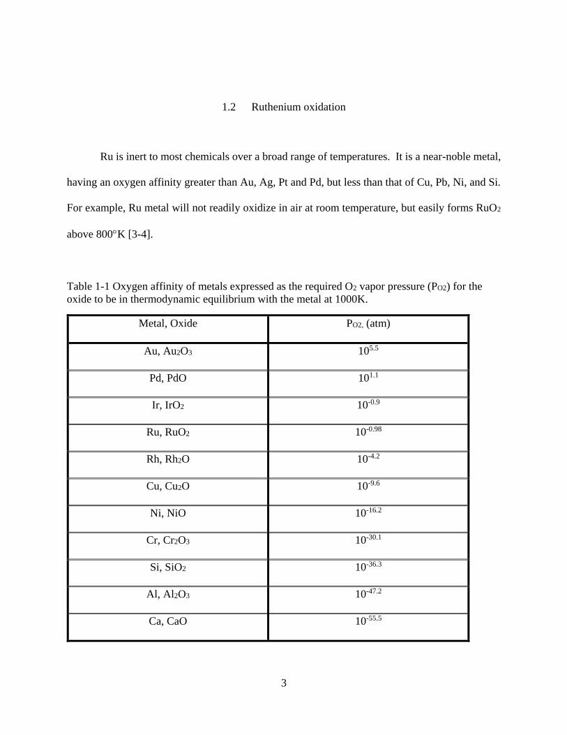
Table 1-1 Oxygen affinity of metals expressed as the required O2 vapor pressure (PO2) for the
oxide to be in thermodynamic equilibrium with the metal at 1000K.
Metal, Oxide PO2, (atm)
Au, Au2O3 105.5
Pd, PdO 101.1
Ir, IrO2 10-0.9
Ru, RuO2 10-0.98
Rh, Rh2O 10-4.2
Cu, Cu2O 10-9.6
Ni, NiO 10-16.2
Cr, Cr2O3 10-30.1
Si, SiO2 10-36.3
Al, Al2O3 10-47.2
Ca, CaO 10-55.5
4
Ru has many naturally occurring isotopes with masses 9, 98, 99, 100, 101, 102, and 104.
The properties of Ru more closely resemble those of Os (also having a hcp crystal structure) than
those of Fe. Ru is a hard grayish-white metal and is used in metal alloys to increase hardness,
primarily with platinum and palladium alloys. It has application as a water-resistant material in the
electronics industry and as a catalyst in industrial fields. It is a p-type conductor. It is a relatively
rare element comprising around 10-7% of the earth crust [5].
The major application of Ru is as thin film resistors and buffer layers in the electronic
industry. Ru is known as an essential homogeneous catalyst to reduce nitric oxides with hydrogen
and is a very active catalyst to produce ammonia. Ru is a good oxidation catalyst in the mbar range,
but under ultra-high vacuum UHV conditions the Ru (0001) is weak catalyst to oxidize CO to CO2
[6]. Surface science studies, under UHV conditions, have shown a variety of structures of oxygen
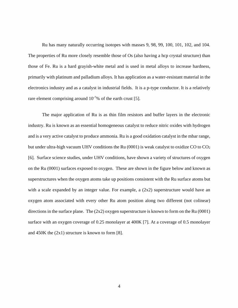
on the Ru (0001) surfaces exposed to oxygen. These are shown in the figure below and known as
superstructures when the oxygen atoms take up positions consistent with the Ru surface atoms but
with a scale expanded by an integer value. For example, a (2x2) superstructure would have an
oxygen atom associated with every other Ru atom position along two different (not colinear)
directions in the surface plane. The (2x2) oxygen superstructure is known to form on the Ru (0001)
surface with an oxygen coverage of 0.25 monolayer at 400K [7]. At a coverage of 0.5 monolayer
and 450K the (2x1) structure is known to form [8].
5
Figure 1-3 STM images show the chemisorbed oxygen on Ru (0001).
At greater oxygen coverage and higher temperature (about 500 K), the Ru (0001) surface
is able to form two additional superstructures, the (2x2)-3O at 0.75 monolayer [9] and (1x1)
structure at 1.0 monolayer [10]. The infrared spectroscopy of the O-Ru stretch vibration is
increased when the O monolayer increased from 521 cm-1 (2x2) O of 0.25 monolayer to 585 cm-1
for (2x1)O of 0.5 monolayer, and the peak at 521 cm-1 decreases in intensity due to more O2
exposure on Ru (0001) surface and the peak shifts up to 585 cm-1. With increased temperature up
to 600K with high O2 exposure on the Ru (0001) surface, the peak at 585cm-1 disappears and a
peak at 640 cm-1 shows up due to the increase of the oxide layer to 0.75 monolayer to (2x2) 3O.
At a higher temperature around 800K, 1.0 monolayer of RuO2 (110) forms on Ru (0001) and the
stretch vibration of (1x1) O is 646 cm-1 [11-15].
The chemisorbed O on RuO2 is weaker than O on Ru (0001), evidenced by the desorption
temperature of chemisorbed O is higher than decomposition temperature of RuO2 in UHV

6
conditions [16]. The different superstructures can be considered different thermodynamic phases
and Figure 1.4 is a plot of the free energy of formation of the phases as a function of oxygen
chemical potential (indicated as a partial pressure at 300K and 600K) to compare their relative
stabilities [17].
Figure 1-4 Calculated free energy O-Ru (0001) structures.
At temperatures of about 500K or below, the exposure of the Ru (0001) surface to oxygen
does not result in the formation of a RuO2 layer on the surface, but at temperatures in range 600-
800 K the oxygen atoms start to form several monolayers of RuO2 on Ru (0001) surface [18].
RuO2 thin films with a (110) orientation have been observed to preferentially grow as a very flat
layer on the Ru (0001) surface at temperatures above 550K. This is surprising, as the (110) RuO2
surface is incommensurate with the Ru (0001) surface. The RuO2 (100) surface is nearly epitaxial
7
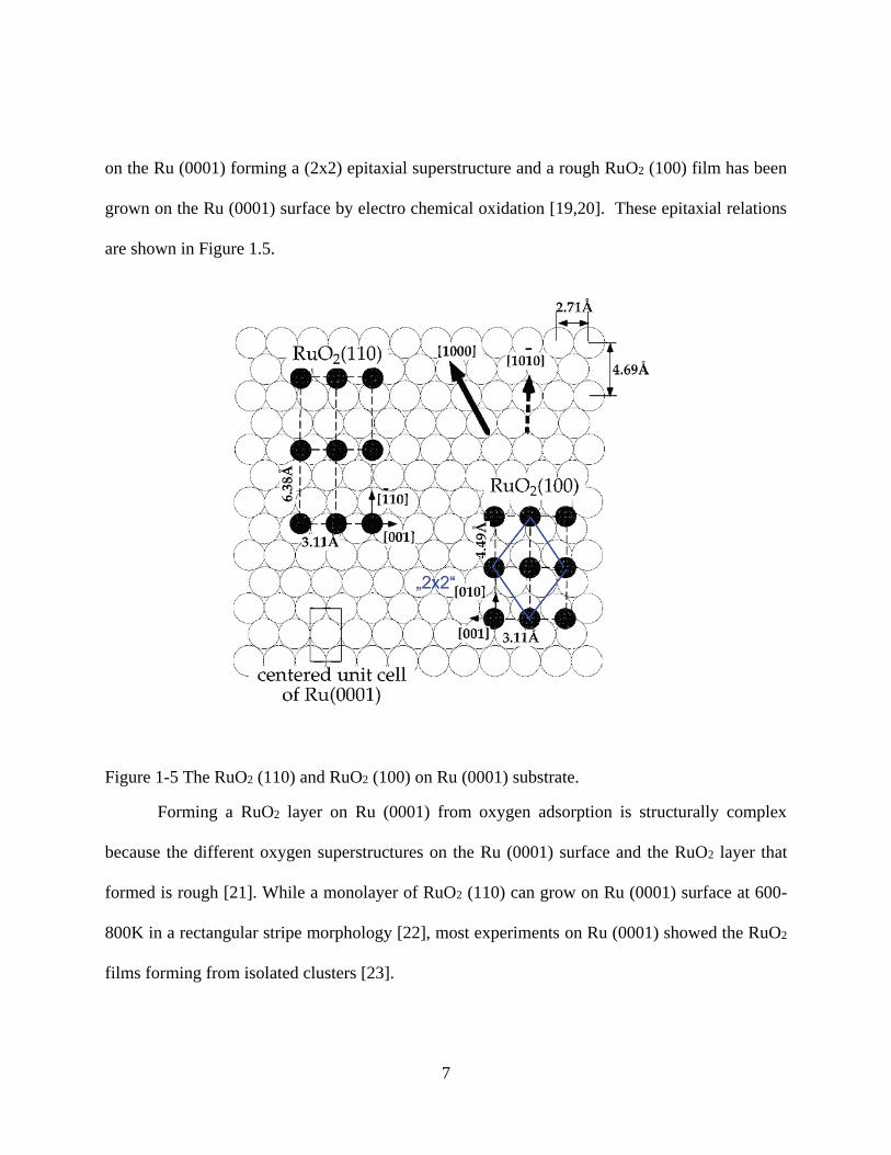
on the Ru (0001) forming a (2x2) epitaxial superstructure and a rough RuO2 (100) film has been
grown on the Ru (0001) surface by electro chemical oxidation [19,20]. These epitaxial relations
are shown in Figure 1.5.
Figure 1-5 The RuO2 (110) and RuO2 (100) on Ru (0001) substrate.
Forming a RuO2 layer on Ru (0001) from oxygen adsorption is structurally complex
because the different oxygen superstructures on the Ru (0001) surface and the RuO2 layer that
formed is rough [21]. While a monolayer of RuO2 (110) can grow on Ru (0001) surface at 600-
800K in a rectangular stripe morphology [22], most experiments on Ru (0001) showed the RuO2
films forming from isolated clusters [23].
8
1.3 Reduction of RuO2 (110) on Ru (0001) surface
The RuO2 which formed on a Ru (0001) surface that raises the Ru resistivity can be easily
reduced. There are many methods to reduce RuO2 (110) to Ru metal by exposing the RuO2 with
reducing agents, such as H2, CO, or methanol at temperature above 150C. Another way is by
heating in vacuum to 550-700C.
1.3.1 Reduction by hydrogen
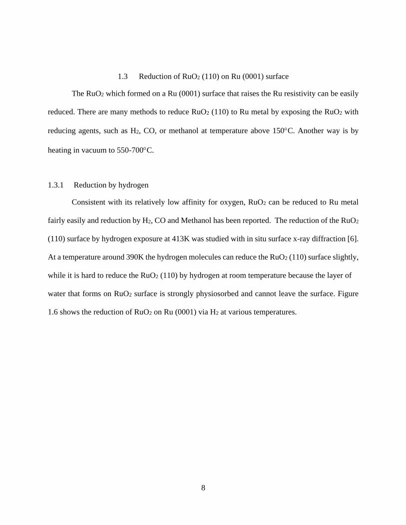
Consistent with its relatively low affinity for oxygen, RuO2 can be reduced to Ru metal
fairly easily and reduction by H2, CO and Methanol has been reported. The reduction of the RuO2
(110) surface by hydrogen exposure at 413K was studied with in situ surface x-ray diffraction [6].
At a temperature around 390K the hydrogen molecules can reduce the RuO2 (110) surface slightly,
while it is hard to reduce the RuO2 (110) by hydrogen at room temperature because the layer of
water that forms on RuO2 surface is strongly physiosorbed and cannot leave the surface. Figure
1.6 shows the reduction of RuO2 on Ru (0001) via H2 at various temperatures.
9
Figure 1-6 Surface X-ray diffraction explain the reduction of RuO2 on Ru (0001) surface via H2
molecules at various temperatures.
1.3.2 Reduction by carbon monoxide
At low pressure, around 10-5 mbar, and a temperature of 420K and an exposure of one-
hour, CO molecules can reduce a monolayer of RuO2 (110) on a Ru (0001) surface. Blume et al.
studied the reduction of RuO2 on a Ru (0001) surface via high pressure XPS and they found the
temperature an important factor wherein below 400K the CO molecules could not fully reduce the
RuO2 [24,25].
10
1.3.3 Reduction by methanol
In a pressure of 10-6 mbar and temperature above 520K, methanol is a good reduction agent
to reduce the RuO2 (110) on Ru (0001). These results done by in situ at pressure 10-6 in XPS [26].
11
CHAPTER 2 BACKGROUND AND MOTIVATION
2.1 Resistivity of thin metal films
The observation of the increase in resistivity for thinner metallic conductors dates back to 1901
[27] and is commonly described as the resistivity size effect. The resistivity size effect was
described by the semi-classical Fuchs-Sondheimer (FS) model in the middle of the last century
[28,29]. This model attributes the resistivity increase to additional electron scattering from
conductor interfaces (surfaces and grain boundaries) when the spacing between such events
approaches the electron mean free path () associated with phonon scattering. The FS model
includes both the surface characteristics and film thickness as parameters. The resistivity of thin
metal films has been primarily studied from two perspectives:
1. The surface science community has studied the change in resistivity of a fixed thickness
of a metal film with an atomically clean surface as the gas species have been absorbed
and desorbed from the surface, with the resistivity generally increasing with the
coverage of the surface by the absorbent species. These studies focus on the surface
characteristics relationship to resistivity, but rarely include thickness effects, due to the
experimental difficulty in control of film thickness during the surface preparation.
2. The thin film community has studied the change in resistivity as a function of thickness
for films having the same surface conditions, typically laboratory air exposed and
contaminated.
12
Recently, interest in the resistivity size effect has been renewed as the dimension of the wires
interconnecting transistors in integrated circuits approach the electron mean free path (EMFP),
commonly designated by (which for Cu at room temperature is 39 nm) [30] and has become a
“Critical Challenge” in the International Technology Roadmap for Semiconductors [31]. The wires
in integrated circuits are typically not atomically clean and readily available for experiments based
on the controlled absorption of gas molecules. Rather, they are buried within layer of a low-density
amorphous silicon oxide dielectric, which makes the study of surface scattering at the metal surface
of the wires more difficult. This dissertation addresses this challenge by a study of surface
scattering at such a buried metal/dielectric interface and demonstrates a means to increase specular
scattering at the interface, allowing a lower resistivity to be obtained.
2.2 Adsorbate induced changes in resistivity of atomically clean metal films
It has been widely observed that for an atomically clean conductor surface, an increase of
resistivity can be observed due to atomic or molecular gas absorption on the surface. This is
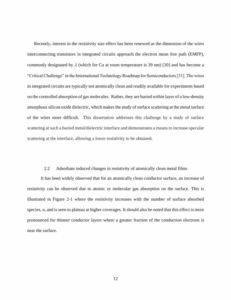
illustrated in Figure 2-1 where the resistivity increases with the number of surface absorbed
species, n, and is seen to plateau at higher coverages. It should also be noted that this effect is more
pronounced for thinner conductor layers where a greater fraction of the conduction electrons is
near the surface.
13
Figure 2-1 Resistivity increased due to gas adsorption on a thin film conductor.
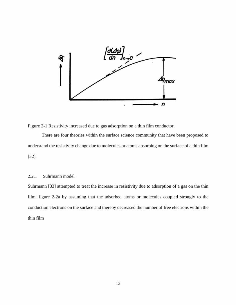
There are four theories within the surface science community that have been proposed to
understand the resistivity change due to molecules or atoms absorbing on the surface of a thin film
[32].
2.2.1 Suhrmann model
Suhrmann [33] attempted to treat the increase in resistivity due to adsorption of a gas on the thin
film, figure 2-2a by assuming that the adsorbed atoms or molecules coupled strongly to the
conduction electrons on the surface and thereby decreased the number of free electrons within the
thin film

14
Figure 2-2 Four theories that have been proposed to understand the resistivity change due to
molecules or atoms absorbing on the surface of a thin film.
The thickness, h, of the thin film and the EMFP, , remain unchanged and due to the
chemical binding of the electrons the upper layer of the metal surface will lose its metallic
properties according this equation.
lim𝑛→0
d (Δρ/ρ)
d𝑛 = K1/ℎ ( 2-1 )
Where is resistivity, h thickness, and K1 is an initial proportionality constant describing the slope
of the resistivity increase with absorbent coverage.
This model failed to account for the extent of the resistivity increase with coverage and also
did not correctly describe the tendency of some adsorbed molecules to donate electrons to the
surface and has since been widely discounted [32].
15
2.2.2 Sachtler model
In this model the resistivity increase with molecular absorption depends on film thickness
and annealing temperature according to:
lim𝑛→0
d (Δρ/ρ)
d𝑛 = K2(ℎ, 𝑇𝐴)/ℎ ( 2-2)
Where K2 is the initial proportionality constant, now dependent on both h and the annealing
temperature, TA. The model describes the resistivity increase as due to a loss of conductor
thickness as a product layer is formed on the surface. This type of resistance increase is observed.
For example, as a Ni film is oxidized, its resistivity can be described with this model. But the
model fails to describe the increases in resistivity observed at a constant conductor layer thickness
that are more scientifically interesting [32].
2.2.3 Fuchs-Sondheimer model
The Fuchs-Sondheimer (FS) model is most widely accepted model to describe the
resistivity size effect and treats both film thickness and surface characteristics. It will be used
extensively in this dissertation. It is a semiclassical model and treats the interaction of the
conduction electrons with the surface as having two possible outcomes. In one case the electron
incident upon the surface reflects back into the interior of the conductor with no loss of momentum.
This is considered a “specular” reflection from the surface and these events do not contribute to
resistivity, as the electron maintains its velocity obtained from the electric field prior to the
collision with the surface, which is necessarily in a direction parallel to the surface. The other case
is considered a “diffuse” reflection, and this is when the electron is modeled to leave the surface
with a loss of momentum, specifically to return to the conductor interior in a random direction
16
with a velocity consistent with the local thermal equilibrium. The primary parameter of the model
is the surface specularity, p, which is equal to one for fully specular surfaces and equal to zero for
fully diffuse surfaces [28,29]. In this model the gas adsorption on the surface will decrease p and
increase resistivity according to
lim𝑛→0
d (Δρ/ρ)
d𝑛 = K3(𝜌𝑜𝑜)/ℎ ( 2-3)
where o is the resistivity of an infinitely thick film (i.e., bulk resistivity) and is the EMFP for
scattering in thick films.
2.2.4 The scattering hypothesis
The scattering hypothesis attributes the increase in resistivity to a variety of mechanisms
that can contribute to the surface scattering. The surface roughness (as a fraction of film thickness)
may increase, especially for metals on an insulating substrate, the impurity contamination level
may also increase for thinner films (e.g., due to diffusion from the substrate, poor vacuum
practices), and thinner polycrystalline films tend to have a smaller grain size which provides for
an increase in grain boundary scattering. All of these can increase the resistivity response to
absorbed gas species. The role of grain boundary scattering has been treated by semiclassical
models similar to that of FS [34] and can be combined with the FS model for polycrystalline films
[35]. This dissertation will focus on the resistivity of single crystal films, and hence the grain
boundary scattering models do not apply. The film purity is clearly an important experimental
variable and commonly controlled by use of inert substrates (single crystal sapphire in this work)
17
and high purity starting materials. The effect of roughness on resistivity is modelled separately and
at very high roughness the porosity of a film can contribute to gas absorption phenomena.
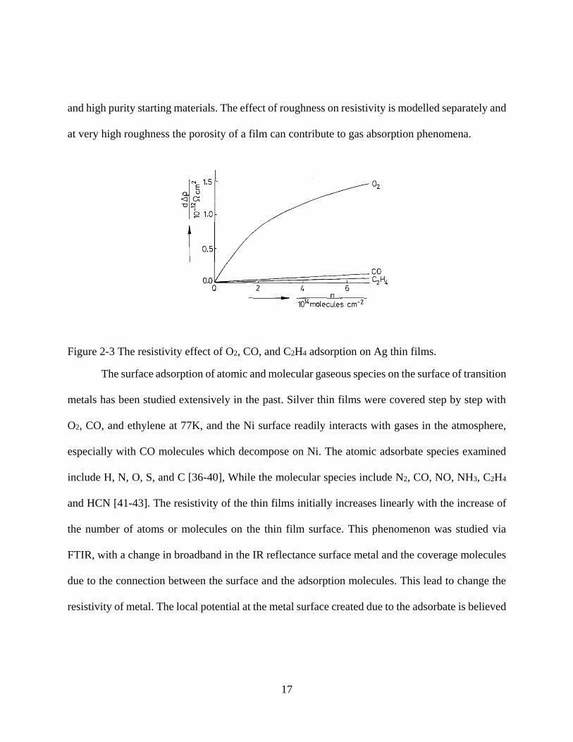
Figure 2-3 The resistivity effect of O2, CO, and C2H4 adsorption on Ag thin films.
The surface adsorption of atomic and molecular gaseous species on the surface of transition
metals has been studied extensively in the past. Silver thin films were covered step by step with
O2, CO, and ethylene at 77K, and the Ni surface readily interacts with gases in the atmosphere,
especially with CO molecules which decompose on Ni. The atomic adsorbate species examined
include H, N, O, S, and C [36-40], While the molecular species include N2, CO, NO, NH3, C2H4
and HCN [41-43]. The resistivity of the thin films initially increases linearly with the increase of
the number of atoms or molecules on the thin film surface. This phenomenon was studied via
FTIR, with a change in broadband in the IR reflectance surface metal and the coverage molecules
due to the connection between the surface and the adsorption molecules. This lead to change the
resistivity of metal. The local potential at the metal surface created due to the adsorbate is believed
18
to increase the scattering of conduction electrons by changing the electron density and increasing
the surface roughness of the metal films [44-54].
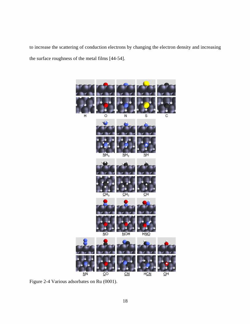
Figure 2-4 Various adsorbates on Ru (0001).
19
2.3 Resistivity due to variation of metal film thickness
The resistivity size effects due to grain boundaries [55-57], surface roughness [58-60], and
scattering at the conductor surfaces [61-64] have been previously described and there is significant
interest in obtaining “specular” metal surfaces with reduced surface scattering to minimize the size
effect resistivity increase [62,65]. In this dissertation, a study of variations in scattering from the
surface of single crystal Ru metal films with variation of the structure and chemistry of the surface
is reported. Interfaces that are significantly specular, air-stable, and resilient to non-reversible
changes, even when encapsulated beneath a dielectric, are observed and described. Within the
surface science literature there are similar studies of resistivity effects due to surface scattering at
metal/vacuum interfaces wherein the adsorption of atoms or molecules on the surface increases
the electrical resistivity of the thin films. These chemical and structural modifications to the surface
are known as adsorbate-induced changes where the electrical resistivity increases with increased
coverage of the adsorbate species on the surface. This increased coverage is understood to increase
the density of scattering sites on the surface. [32]. The adsorbate species can also form molecular
compound complexes with the metallic thin films and thereby change the electronic states at the
surface [66]. Thus, for a careful study of the resistivity size effect more than just the film sheet
resistance and thickness are needed. In addition, the roughness, structure and chemistry of the
surface must be known, and processing details, such as the annealing temperature, are also desired
to provide insight to the surface characteristics. These prior studies typically explored variations
in surface chemistry or structure at an exposed metal/vacuum or metal/vapor interface. Other prior
work includes studies of large-scale roughness [58] and atomic scale roughness induced resistivity
20
wherein the presence of atomically flat regions on the metal surface were found to reduce surface
scattering [67].
Ru, being a nearly noble metal from the platinum group, is being investigated by
researchers for semiconductor applications. Ru has desirable properties that may allow it to replace
Cu as an interconnect metal, such as high electrical conductivity, large work function, and small
resistivity size effect. Nanoscale Ru may have lower resistivity than nanoscale Cu and can be
expected to have greater stability due to its higher melting point [65, 68-72]. Ruthenium has also
been studied as a diffusion barrier in the copper metallization process [5] and has potential for
integration in semiconductor manufacturing, i.e., it known to be compatible with semiconductor
manufacturing facilities and not pose a threat of contamination and yield loss. The electrical
resistivity of RuO2 is about 35.2 μΩ·cm at room temperature and higher than that of polycrystalline
metallic ruthenium (about 7.36 μΩ·cm).
The encapsulation material used in our studies, SiO2, has been used in many modern
technologies and is studied here as an example of an amorphous dielectric. In contrast, recent
studies of thin ordered silicon dioxide films grown on Ru (0001) have used XPS, low energy
electron diffraction (LEED), and scanning tunneling microscopy wherein these techniques were
used to study the epitaxial growth of SiO2 layers on Ru (0001).
21
Figure 2-5 SiO2 on Ru (0001), (a) O-poor (b) O-rich.
A silicon dioxide thin film when grown as a monolayer consists of SiO4 tetrahedra that
form a strong bond with Ru (0001) surface due to corner sharing of Si-O-Ru bonds. The limitation
for this is the stoichiometry of the silicon dioxide, which is usually SiO2.5 and not SiO2 because
not all SiO4 tetrahedron corners are shared with another SiO4 tetrahedron. When the silicon dioxide
thickness is increased beyond a monolayer, the film forms a bilayer of two strongly bonded corner-
sharing SiO4 tetrahedron that have only weak bonding to the Ru (0001) surface, as the bonding to
the Ru surface is due to dispersive forces and not by the monolayers of Si-O. The range of
amorphous silicatene rings are from 4-membered to 9-membered rings, while the crystalline
silicatene layer has only 6-membered rings [73-76].
22
Figure 2-6 (a) Atomic structure of an ideal double-layer silicatene on Ru (0001). (b) STM image
of crystalline and amorphous structures of the silicatene.
Another study of thin ordered ultrathin aluminum oxide film grown on Ru (0001) surface
has used XPS, low energy ion scattering (LEIS), (LEED), scanning tunneling microscopy (STM)
and high-resolution electron loss spectroscopy (HRELS) and deposited aluminum in an ambient
of oxygen. The thin film growth at 300K is two-dimensional while the thin film growth at 1170K
is three dimensional [77].
In the present work, we study amorphous SiO2 and Al2O3 grown in vacuum at room
temperature on epitaxial Ru (0001)/sapphire (0001) and focus on the interaction of the deposition
itself and subsequent anneals in oxidizing and reducing gases on the buried SiO2/Ru and Al2O3/Ru
interfaces and relate these to changes in surface scattering. In the current work, resistivity
measurements as a function thickness and as a function of chemical and/or structural changes at a
buried metal/dielectric oxide interface are reported. X-ray photoelectron spectroscopy (XPS) is
used to determine the chemical bonding at the buried interface, while X-ray reflectivity (XRR) is

23
used to determine interfacial roughness of metal upper surface. For the metal/dielectric interface
study, we focus on single crystal 20 nm Ru on sapphire as our conductor and amorphous SiO2.
Our choice of the metal and dielectric is motivated by the different oxygen affinities of Si and Ru,
which allows desirable control of experimental conditions at the metal/dielectric interface.
24
CHAPTER 3 EXPERIMENTAL
3.1 Introduction
The properties of thin films are reliant on many features such as substrate materials,
substrate temperature, the technique of deposition, ambient gas pressure, and deposition rate.
Modern technology can assist to deposit thin films with specific properties such as low porosity,
thermal stability, adhesion, and desirable stoichiometry. There are many procedures for production
of thin films such as physical vaper deposition (PVD), chemical vaper deposition (CVD), sol-gel,
atomic layer deposition, and molecular beam epitaxy. Understanding of the growth procedures
with careful control allows us to deposit thin films with specific thicknesses that can be on the
atomic/molecular level and obtain suitable thin films. The quality of the thin film depends on the
optimization of the deposition procedure. In this chapter the method by which the Ru, Ru/SiO2,
Ru/Al2O3 thin film samples are prepared, sputtering, is described in general. Subsequently, the
characterization techniques for the samples, by X-ray diffraction (XRD), X-ray reflectivity (XRR),
X-ray photoelectron spectroscopy (XPS), low energy electron diffraction (LEED), and four-point
sheet resistance measurements are described, and the details of the specific processing used for the
samples is described in detail.
3.2 Sputter deposition
Sputtering involves dislodging atoms or molecules from a target, the source material, to
deposit on a substrate surface through the impact of gaseous ions. Evaporation and CVD
techniques do not have advantages compared to sputtering, which can have easy control of
25
composition, and the thin films have more purity and can be deposited at lower temperature
compared to CVD.
PVD techniques have a wide range of applications, from decorative films to high
temperature superconductors. The rate of deposition can vary from angstroms to millimeters of
film per minute. PVD techniques are suitable for many materials such as inorganic alloys and
compounds as well as organic materials. The PVD coating of materials by deposition in vacuum
often allows a unique ability to control material properties by controlling the bombardment of the
growing film with ions, electrons, and neutral species during the deposition process. There are
many PVD techniques that differ based on their ability to control the growth conditions. Cathodic
arc deposition uses an arc discharge to generate ions of the film material which can then be directed
towards the substrate with a wide range of controlled energies to effectively implant the ions into
the film. This technique can provide very hard coatings (e.g., diamond-like amorphous carbon).
Evaporation is a technique in which the film material is heated in vacuum to initiate sublimation
or evaporation and the source atoms travel as non-colliding vapor atoms to the substrate where
they condense back to a solid phase and form the film. Magnetron sputtering uses a controlled
vacuum in which a partial pressure on an inert gas is maintained (typically Ar at ~5 x 10⁻⁷
atmospheres). A direct current (DC) a used for sputtering a conductive target while radio frequency
(RF) is used for non-conductive targets.

26
Figure 3-1 Geometry of sputtering deposition.
A negative voltage is present on a target composed of the material to be used to form the film.
This voltage attracts positively charged inert gas ions that impact the target with sufficient energy
to cause the release of target atoms (known as sputtering) as well as electrons. The former
condenses on the substrate to form a film while the latter undergo collisions with the inert gas
atoms, forming a plasma and maintaining a supply of ions to perpetuate the sputtering of atoms
from the target. The presence of the plasma allows inert gas atoms or electrons to be attracted to
the substrate for the bombardment to control film properties [77,78].

27
3.3 XRD and XRR characterization
3.3.1 XRD characterization
X-ray diffraction is a remarkable analytical technique to identify the crystalline structure of
materials. This information is obtained from their diffraction pattern. That diffraction occurs when
X-ray incident beam interacts with the atoms of the sample and is coherently scattered. The XRD
studies reported here were performed using a Panalytical X’pert3 MRD system with a copper K
radiation source (=1.54056A) with a graded multilayer mirror for the incident beam and the 1D
PIXcel detector for the diffracted beam.
3.3.2 XRR characterization
XRR is a technique that uses the full thickness of a thin film layer to form a coherent
interference pattern. The layer thicknesses and roughnesses of our thin film samples were
characterized by XRR with same X-ray optical configuration used for the XRD measurements.
The XRR data were interpreted using the PANalytical X’Pert Reflectivity software. The samples
without a SiO2 or Al2O3 overlayer were modeled as a sapphire/Ru/RuO2 structure, the samples
with the SiO2 overlayer as sapphire/Ru/RuO2/SiO2, and the samples with the Al2O3 overlayer as a
sapphire/Ru/RuO2/Al2O3 structure. Bulk density values of 3.989 g/cm3, 12.4 g/cm3, 6.97 g/cm3,
and 2.196 g/cm3 were used for the sapphire, Ru, RuO2, and SiO2, respectively.

28
Figure 3-2 Representative XRR data from a 4.6nm thick SiO2 on a 20.8nm-thick Ru (0001) layer.
(a) upper (black) curve is for measured data shifted by a factor of 101 for clarity and (b) the
lower (red) curve is for fitted model.
3.4 Four-Point Resistivity Measurement
The resistivity measurement is made in accordance to the delta (output voltage)
measurement test circuit, see Fig 3-3, where in the Keithley source meter 2400 is a bipolar fixed-
amplitude current source which reverses polarity at a fixed interval and communicates the polarity
reversal to the Keithely nanovoltmeter model 2812 via the 8501 Trigger Link Cable. This allows
resistance to be made independent of any thermally induced DC voltage that may be present. This
resistance was measured in a sample contacted in the Van der Pauw geometry, which, as
implemented, has less than 3% of error [79].
29
Figure 3-3 Diagram of the Van der Pauw geometry dipping probe
The resistance according to above figure is calculated as follows.
𝑅1243 =𝑉43
𝐼12 ( 3-1 )
where R= Resistance, V= Voltage, and I= Current
Where R1243 indicates where current was sourced 1→ 2 and voltage was measured 3 → 4. To
calculate the sheet resistance, Rs, the van der Pauw method makes two measurements. First, it
sources current along the horizontal edge of the film and measures the voltage drop across the
opposite edge. Then it sources the current along the vertical edge of the film and measures the
voltage drop across the opposite edge. The average vertical and horizontal resistances are
calculated
𝑅𝑣𝑒𝑟𝑡𝑖𝑐𝑎𝑙 =𝑅1243+ 𝑅4312
2 ( 3-2)
𝑅ℎ𝑜𝑟𝑖𝑧𝑜𝑛𝑡𝑎𝑙 =𝑅1423+ 𝑅2314
2 ( 3-3)
A numerical method is then used to solve for the sheet resistance, Rs
𝑒(−𝜋𝑅𝑣𝑒𝑟𝑡𝑖𝑐𝑎𝑙/𝑅𝑠) + 𝑒(−𝜋𝑅ℎ𝑜𝑟𝑖𝑧𝑜𝑛𝑡𝑎𝑙/𝑅𝑠) = 1 ( 3-4)
expressed in ohms per square or Ω/. Finally, the resistivity, of the sample is determined
as the product of Rs and the thickness, h [79-81].
30
𝜌 = 𝑅𝑠ℎ ( 3-5)
3.5 Sample preparation details
The deposition and annealing of six series of Ru, Ru/SiO2, and Ru/Al2O3 thin film samples are
described in this chapter. The first, second, and third sample series are variations in thicknesses
for Ru films on sapphire while the fourth, fifth, and sixth series utilize bilayered Ru/SiO2 and
Ru/Al2O3 at a single Ru thickness to elucidate surface scattering phenomena.
3.5.1 Ru single crystal film deposition
The Ru thin films were sputter deposited on single-side polished two-inch diameter (0001)
Al2O3 sapphire substrates obtained from MTI Corporation. Prior to deposition, the as-received
sapphire substrates were pre-conditioned by heating in a tube furnace in air at 1000C for 30
minutes to remove adsorbed contaminants and loaded within the deposition chamber within 5
minutes to minimize the possibility of recontamination. The deposition system used was an
ATC2200 UHV sputtering system obtained from AJA International Inc. equipped with a loadlock
chamber for sample introduction and operated with a base vacuum in the low 10-8 Torr range. DC
magnetron sputtering in a point-of-use purified Ar gas ambient at 4 mTorr from a two-inch
diameter Ru (99.95%) target was used for the Ru film depositions. The Ru deposition power of
200W was used to obtain a deposition rate 0.13 nm/s. In the deposition chamber, the sapphire
substrates were heated to 400C, 500C, 600C, and 700C (for sample series one) 350C (for
sample series two) or 700C (for sample series three, four, five, and six) for 20 minutes prior to
deposition and maintained at that temperature during the deposition process. The deposition time

31
was varied to obtain Ru films of the desired thickness. Six series of samples were prepared, as
described in Table 1.
Table 3-1 Listing of sample series studied.
Sample Series Ru Layer Thickness (nm) Dielectric Overlayer Deposition temperature
1 10 to 80 None 400C, 500C, 600C, 700C
2 8 to 124 None 350C
3 20 to 80 None 700C
4 20 SiO2 Evaporation 700C
5 20 SiO2 Sputtering 700C
6 20 Al2O3 Sputtering 700C
Sample series one was made in the thickness range of 10 nm to 80 nm at temperatures ranging
from 400C to 700C. Sample series two was made in the thickness range of 8 nm to 124 nm.
Sample series three was made in the thickness range of 20 nm to 80 nm. The fourth, fifth, and six
experimental series each consisted of samples cut from a single wafer, all having a deposited Ru
thickness of 20 nm. After the initial Ru sputter deposition, the ruthenium thin films were allowed
to cool to room temperature in the sputter deposition chamber and removed from the vacuum
system and exposed to the ambient laboratory atmosphere. The sapphire wafers with deposited
ruthenium thin films were subsequently cut into 7 mm by 7 mm square pieces by a CO2 laser
incident upon the back side of the wafer to avoid the laser reflection from the shiny Ru thin film,
we found the optimal performance to cut the Ru thin films on sapphire was using speed 6
millimeters per second and power of 5W.
32
3.5.2 Anneal to 700C
After cutting, samples series one was annealed at 700C in one atmosphere of flowing
Ar/H2 3% wherein the annealing temperature was increased from room temperature to 700C in
30 minutes and held for 120 minutes and allowed to cool to room temperature. The thickness and
resistivity for these annealed sample are described in Table 3-2.
33
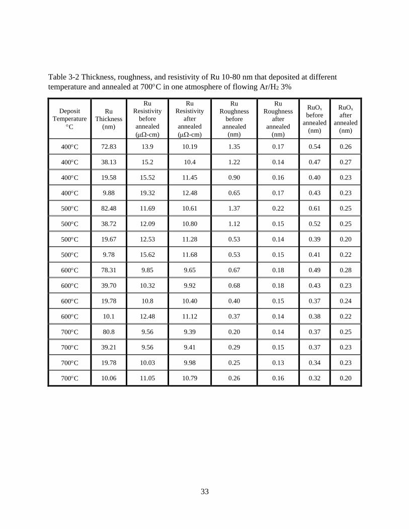
Table 3-2 Thickness, roughness, and resistivity of Ru 10-80 nm that deposited at different
temperature and annealed at 700C in one atmosphere of flowing Ar/H2 3%
Deposit
Temperature
C
Ru
Thickness
(nm)
Ru
Resistivity
before
annealed
(-cm)
Ru
Resistivity
after
annealed
(-cm)
Ru
Roughness
before
annealed
(nm)
Ru
Roughness
after
annealed
(nm)
RuOx
before
annealed
(nm)
RuOx
after
annealed
(nm)
400C 72.83 13.9 10.19 1.35 0.17 0.54 0.26
400C 38.13 15.2 10.4 1.22 0.14 0.47 0.27
400C 19.58 15.52 11.45 0.90 0.16 0.40 0.23
400C 9.88 19.32 12.48 0.65 0.17 0.43 0.23
500C 82.48 11.69 10.61 1.37 0.22 0.61 0.25
500C 38.72 12.09 10.80 1.12 0.15 0.52 0.25
500C 19.67 12.53 11.28 0.53 0.14 0.39 0.20
500C 9.78 15.62 11.68 0.53 0.15 0.41 0.22
600C 78.31 9.85 9.65 0.67 0.18 0.49 0.28
600C 39.70 10.32 9.92 0.68 0.18 0.43 0.23
600C 19.78 10.8 10.40 0.40 0.15 0.37 0.24
600C 10.1 12.48 11.12 0.37 0.14 0.38 0.22
700C 80.8 9.56 9.39 0.20 0.14 0.37 0.25
700C 39.21 9.56 9.41 0.29 0.15 0.37 0.23
700C 19.78 10.03 9.98 0.25 0.13 0.34 0.23
700C 10.06 11.05 10.79 0.26 0.16 0.32 0.20
34
3.5.3 Step anneal to 950C
After cutting, all the samples were annealed (ex-situ) step-wise in one atmosphere of flowing
Ar/H2 3% to a maximum temperature of 950C. The annealing temperature was increased from
room temperature to 350C and stabilized at 350C for 30 minutes. After that the temperature was
further increased in steps of 100C and held for 30 minutes at each temperature. This increasing
temperature portion of the anneal continued up to the maximum temperature of 950C, at which
temperature the sample was held for 30 minutes. Subsequently, the temperature was decreased in
steps of 100C and held at each temperature for 60 minutes until 150C was reached, after which
the sample was allowed to cool to room temperature. This was the basic processing (Ru film
deposition and ex-situ 950C Ar/H2 step anneal) which was performed for all of the sample series
2 though 6.
3.5.4 Additional anneals for series 3
The third sample series was subjected to subsequent additional oxidizing and reducing
annealing treatments of the Ru films. The anneals were in one atmosphere of Ar/H2 3%, or air, at
a temperature of 300C wherein the desired temperature was held for 2 hours, and then furnace
cooled to room temperature. These anneals and the sequence in which they were performed is
described in Table 3-3.
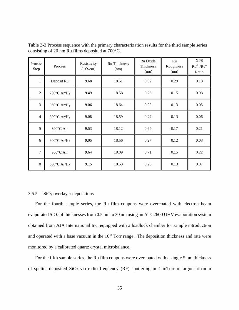
35
Table 3-3 Process sequence with the primary characterization results for the third sample series
consisting of 20 nm Ru films deposited at 700C.
Process
Step Process
Resistivity
(-cm)
Ru Thickness
(nm)
Ru Oxide
Thickness
(nm)
Ru
Roughness
(nm)
XPS
Ruδ+/Ru0
Ratio
1 Deposit Ru 9.68 18.61 0.32 0.29 0.18
2 700C Ar/H2 9.49 18.58 0.26 0.15 0.08
3 950C Ar/H2 9.06 18.64 0.22 0.13 0.05
4 300C Ar/H2 9.08 18.59 0.22 0.13 0.06
5 300C Air 9.53 18.12 0.64 0.17 0.21
6 300C Ar/H2 9.05 18.56 0.27 0.12 0.08
7 300C Air 9.64 18.09 0.71 0.15 0.22
8 300C Ar/H2 9.15 18.53 0.26 0.13 0.07
3.5.5 SiO2 overlayer depositions
For the fourth sample series, the Ru film coupons were overcoated with electron beam
evaporated SiO2 of thicknesses from 0.5 nm to 30 nm using an ATC2600 UHV evaporation system
obtained from AJA International Inc. equipped with a loadlock chamber for sample introduction
and operated with a base vacuum in the 10-8 Torr range. The deposition thickness and rate were
monitored by a calibrated quartz crystal microbalance.
For the fifth sample series, the Ru film coupons were overcoated with a single 5 nm thickness
of sputter deposited SiO2 via radio frequency (RF) sputtering in 4 mTorr of argon at room

36
temperature with 165 W of power using a two-inch diameter SiO2 (99.95%) target. The rate of
deposition for SiO2 on the ruthenium thin films was 0.03 nm/s. The thickness of the overlayer was
chosen to be sufficiently thin to allow subsequent XPS characterization of the buried Ru/SiO2
interface.
3.5.6 Al2O3 overlayer depositions
For sample series six, the Ru film coupons were overcoated with a single 6 nm thickness
of sputter deposited Al2O3 via RF sputtering in 4 mTorr of argon at room temperature with 200 W
of power using a two-inch diameter Al2O3 (99.95%) target. The rate of deposition for Al2O3 on the
ruthenium thin films was 0.02 nm/s.
3.5.7 Additional anneals for series 5
The fifth sample series was also subjected to subsequent additional oxidizing and reducing
annealing treatments of the Ru/SiO2 bilayer films, including a repeat of the 950C Ar/H2 step
anneal. The lower temperature anneals were in one atmosphere of one of the following gases:
flowing Ar/H2 3%, Ar/O2 20%, or air, at temperatures 300C, 400C, or 500C wherein the desired
temperature was held for 2 hours, and then furnace cooled to room temperature. These anneals
and the sequence in which they were performed is described in Table 3-4.
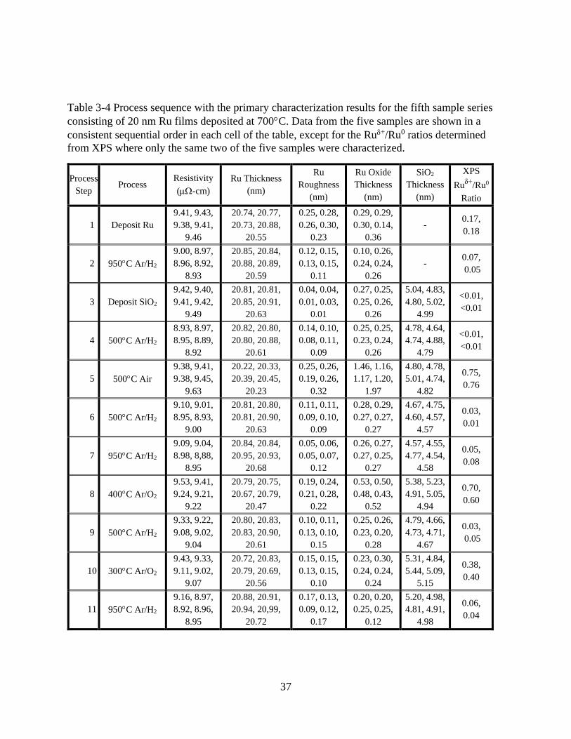
37
Table 3-4 Process sequence with the primary characterization results for the fifth sample series
consisting of 20 nm Ru films deposited at 700C. Data from the five samples are shown in a
consistent sequential order in each cell of the table, except for the Ru+/Ru0 ratios determined
from XPS where only the same two of the five samples were characterized.
Process
Step Process
Resistivity
(-cm)
Ru Thickness
(nm)
Ru
Roughness
(nm)
Ru Oxide
Thickness
(nm)
SiO2
Thickness
(nm)
XPS
Ruδ+/Ru0
Ratio
1 Deposit Ru
9.41, 9.43,
9.38, 9.41,
9.46
20.74, 20.77,
20.73, 20.88,
20.55
0.25, 0.28,
0.26, 0.30,
0.23
0.29, 0.29,
0.30, 0.14,
0.36
- 0.17,
0.18
2 950C Ar/H2
9.00, 8.97,
8.96, 8.92,
8.93
20.85, 20.84,
20.88, 20.89,
20.59
0.12, 0.15,
0.13, 0.15,
0.11
0.10, 0.26,
0.24, 0.24,
0.26
- 0.07,
0.05
3 Deposit SiO2
9.42, 9.40,
9.41, 9.42,
9.49
20.81, 20.81,
20.85, 20.91,
20.63
0.04, 0.04,
0.01, 0.03,
0.01
0.27, 0.25,
0.25, 0.26,
0.26
5.04, 4.83,
4.80, 5.02,
4.99
<0.01,
<0.01
4 500C Ar/H2
8.93, 8.97,
8.95, 8.89,
8.92
20.82, 20.80,
20.80, 20.88,
20.61
0.14, 0.10,
0.08, 0.11,
0.09
0.25, 0.25,
0.23, 0.24,
0.26
4.78, 4.64,
4.74, 4.88,
4.79
<0.01,
<0.01
5 500C Air
9.38, 9.41,
9.38, 9.45,
9.63
20.22, 20.33,
20.39, 20.45,
20.23
0.25, 0.26,
0.19, 0.26,
0.32
1.46, 1.16,
1.17, 1.20,
1.97
4.80, 4.78,
5.01, 4.74,
4.82
0.75,
0.76
6 500C Ar/H2
9.10, 9.01,
8.95, 8.93,
9.00
20.81, 20.80,
20.81, 20.90,
20.63
0.11, 0.11,
0.09, 0.10,
0.09
0.28, 0.29,
0.27, 0.27,
0.27
4.67, 4.75,
4.60, 4.57,
4.57
0.03,
0.01
7 950C Ar/H2
9.09, 9.04,
8.98, 8,88,
8.95
20.84, 20.84,
20.95, 20.93,
20.68
0.05, 0.06,
0.05, 0.07,
0.12
0.26, 0.27,
0.27, 0.25,
0.27
4.57, 4.55,
4.77, 4.54,
4.58
0.05,
0.08
8 400C Ar/O2
9.53, 9.41,
9.24, 9.21,
9.22
20.79, 20.75,
20.67, 20.79,
20.47
0.19, 0.24,
0.21, 0.28,
0.22
0.53, 0.50,
0.48, 0.43,
0.52
5.38, 5.23,
4.91, 5.05,
4.94
0.70,
0.60
9 500C Ar/H2
9.33, 9.22,
9.08, 9.02,
9.04
20.80, 20.83,
20.83, 20.90,
20.61
0.10, 0.11,
0.13, 0.10,
0.15
0.25, 0.26,
0.23, 0.20,
0.28
4.79, 4.66,
4.73, 4.71,
4.67
0.03,
0.05
10 300C Ar/O2
9.43, 9.33,
9.11, 9.02,
9.07
20.72, 20.83,
20.79, 20.69,
20.56
0.15, 0.15,
0.13, 0.15,
0.10
0.23, 0.30,
0.24, 0.24,
0.24
5.31, 4.84,
5.44, 5.09,
5.15
0.38,
0.40
11 950C Ar/H2
9.16, 8.97,
8.92, 8.96,
8.95
20.88, 20.91,
20.94, 20,99,
20.72
0.17, 0.13,
0.09, 0.12,
0.17
0.20, 0.20,
0.25, 0.25,
0.12
5.20, 4.98,
4.81, 4.91,
4.98
0.06,
0.04
38
3.5.8 Additional anneals for series 6
The sixth sample series was also subjected to subsequent additional oxidizing and reducing
annealing treatments of the Ru/ Al2O3 bilayer films, including a repeat of the 950C Ar/H2 anneal.
The temperature anneals were in one atmosphere in Ar/H2 3%, or air, at a temperature of 500C
wherein the desired temperature was held for 2 hours, and then furnace cooled to room
temperature. These anneals and the sequence in which they were performed is described in Table
3-5.
Table 3-5 Process sequence with the primary characterization results for the sixth sample series
consisting of 20 nm Ru films deposited at 700C. Data from the three samples are shown in a
consistent sequential order in each cell of the table.
Process
step Process
Resistivity
(µΩ-cm)
Ru thickness
(nm)
Ru roughness
(nm)
RuOx
thickness (nm)
1. Deposit Ru 9.69, 9.70,
9.67
19.67, 19.80,
19.82
0.37, 0.34,
0.34
0.35, 0.29,
0.30
2. 950°C Ar/H2 9.02, 9.03,
9.05
19.71, 19.83,
19.87
0.15, 0.14,
0.15
0.22, 0.19,
0.22
3. Deposit Al2O3 10.09, 10,05,
10.13
19.66, 19.82,
19.84
0.15, 0.16,
0.14
0.18, 0.12,
0.19
4. 500°C Ar/H2 9.32, 9.27,
9.36
19.69, 19.81,
19.79
0.13, 0.15,
0.15
0.21, 0.24,
0.25
5. 500°C Air 9.61, 9.58,
9.67
19.35, 19.39,
19.34
0.22, 0.24,
0.25
0.86, 0.97,
1.03
6. 500°C Ar/H2 9.44, 9.42,
9.49
19.67, 19.70,
19.69
0.15, 0.15,
0.17
0.29, 0.32,
0.36
7. 500°C Air 9.88, 9.87,
9.94
19.31, 19.32,
19.28
0.24, 0.20,
0.21
0.91, 0.99,
1.06
8. 500°C Ar/H2 9.68, 9.66,
9.72
19.62, 19.66,
19.59
0.12, 0.16,
0.17
0.38, 0.34,
0.39
9. 500°C Air 10.13, 10.09,
10.21
19.28, 19.30,
19.27
0.19, 0.21,
0.22
0.78, 0.95,
1.10
10. 500°C Ar/H2 9.62, 9.72,
9.74
19.61, 19.68,
19.59
0.16, 0.16,
0.17
0.33, 0.35,
0.39
11. 950°C Ar/H2 9.52, 9.61,
9.66
19.69, 19.76,
19,77
0.16, 0.15,
0.17
0.23, 0.27,
0.30
39
CHAPTER 4 SINGLE CRYSTAL RUTHENIUM FILMS
The characterization of the Ru thin film samples by XRD, XRR, XPS, LEED, and four-point
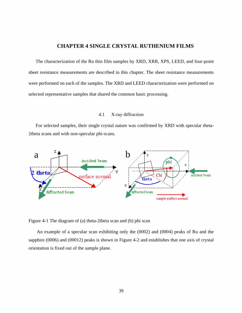
sheet resistance measurements are described in this chapter. The sheet resistance measurements
were performed on each of the samples. The XRD and LEED characterization were performed on
selected representative samples that shared the common basic processing.
4.1 X-ray diffraction
For selected samples, their single crystal nature was confirmed by XRD with specular theta-
2theta scans and with non-specular phi-scans.
Figure 4-1 The diagram of (a) theta-2theta scan and (b) phi scan
An example of a specular scan exhibiting only the (0002) and (0004) peaks of Ru and the
sapphire (0006) and (00012) peaks is shown in Figure 4-2 and establishes that one axis of crystal
orientation is fixed out of the sample plane.
a b

40
Figure 4-2 Specular XRD scan for a Ru film on sapphire (0001) deposited at 700ºC with
thickness d = 39.8 nm.
Non-specular phi scans at chi equal to 57.71 and two-theta equal to 84.68 were performed
to examine the crystallographic orientation of the Ru film crystallites within the sample plane.
The six fold symmetry of the Ru 1122 peaks was observed establishing that a single fixed in-
plane crystallographic orientation is present. The combinations of the two fixed crystallographic
directions for the crystallites establishes the film as single crystal in nature, i.e., all the crystallites
present have the same orientation, hence they are not separate crystallites but part of a single large
crystal. An additional non-specular phi scan at chi equal to 42.3 and two-theta equal to 57.499
was performed to observe the six-fold symmetry of the sapphire 1126 peaks of the single crystal
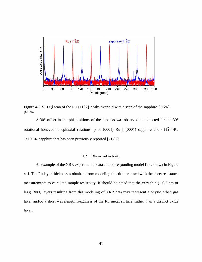
sapphire substrate. These two phi scans are shown in Figure 4-3.
41
Figure 4-3 XRD scan of the Ru 1122 peaks overlaid with a scan of the sapphire 1126
peaks.
A 30 offset in the phi positions of these peaks was observed as expected for the 30
rotational honeycomb epitaxial relationship of (0001) Ru || (0001) sapphire and <1120>Ru
||<1010> sapphire that has been previously reported [71,82].
4.2 X-ray reflectivity
An example of the XRR experimental data and corresponding model fit is shown in Figure
4-4. The Ru layer thicknesses obtained from modeling this data are used with the sheet resistance
measurements to calculate sample resistivity. It should be noted that the very thin (~ 0.2 nm or
less) RuO2 layers resulting from this modeling of XRR data may represent a physiosorbed gas
layer and/or a short wavelength roughness of the Ru metal surface, rather than a distinct oxide
layer.
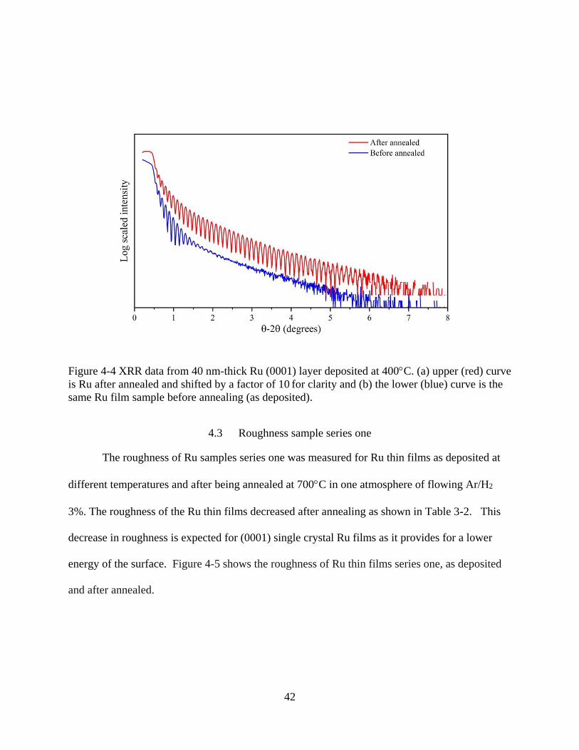
42
Figure 4-4 XRR data from 40 nm-thick Ru (0001) layer deposited at 400C. (a) upper (red) curve
is Ru after annealed and shifted by a factor of 10 for clarity and (b) the lower (blue) curve is the
same Ru film sample before annealing (as deposited).
4.3 Roughness sample series one
The roughness of Ru samples series one was measured for Ru thin films as deposited at
different temperatures and after being annealed at 700C in one atmosphere of flowing Ar/H2
3%. The roughness of the Ru thin films decreased after annealing as shown in Table 3-2. This
decrease in roughness is expected for (0001) single crystal Ru films as it provides for a lower
energy of the surface. Figure 4-5 shows the roughness of Ru thin films series one, as deposited
and after annealed.
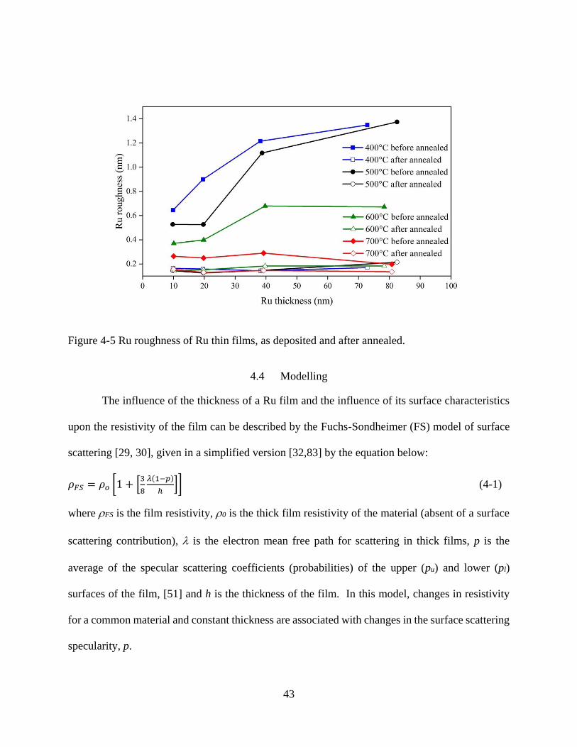
43
Figure 4-5 Ru roughness of Ru thin films, as deposited and after annealed.
4.4 Modelling
The influence of the thickness of a Ru film and the influence of its surface characteristics
upon the resistivity of the film can be described by the Fuchs-Sondheimer (FS) model of surface
scattering [29, 30], given in a simplified version [32,83] by the equation below:
𝜌𝐹𝑆 = 𝜌𝑜 [1 + [3
8
𝜆(1−𝑝)
ℎ]] (4-1)
where FS is the film resistivity, 0 is the thick film resistivity of the material (absent of a surface
scattering contribution), is the electron mean free path for scattering in thick films, p is the
average of the specular scattering coefficients (probabilities) of the upper (pu) and lower (pl)
surfaces of the film, [51] and h is the thickness of the film. In this model, changes in resistivity
for a common material and constant thickness are associated with changes in the surface scattering
specularity, p.
44
From inspection, is it clear that and p can be varied over a range of values and not result
in a change to the model’s prediction of resistivity versus thickness (FS versus h), as long as the
product of (1-p) and is maintained constant, i.e. they cannot be uniquely determined by fitting to
experimental data, only this product is determined. Given a value chosen for , then the average
value of p can be determined from the experimental fitting (for example as p = 50%), but this is
still not unique as this may be interpreted as both upper and lower surfaces having a 50%
probability of specular reflection, or as one surface having a 0% probability and the other having
a 100% probability of specular reflection of electrons [83]. The assumption of fully diffuse surface
scattering from both upper and lower surfaces (p = 0%), is often made in the interpretation of
experimentally measured results, particularly for studies of Cu films and lines [47]. In this work,
we will study variations of resistivity as a result of changes in surface scattering, and, hence, will
need a range of specularity values to correspond to the range of resistivity observed. In this case
we will necessarily deviate from the p = 0% assumption.
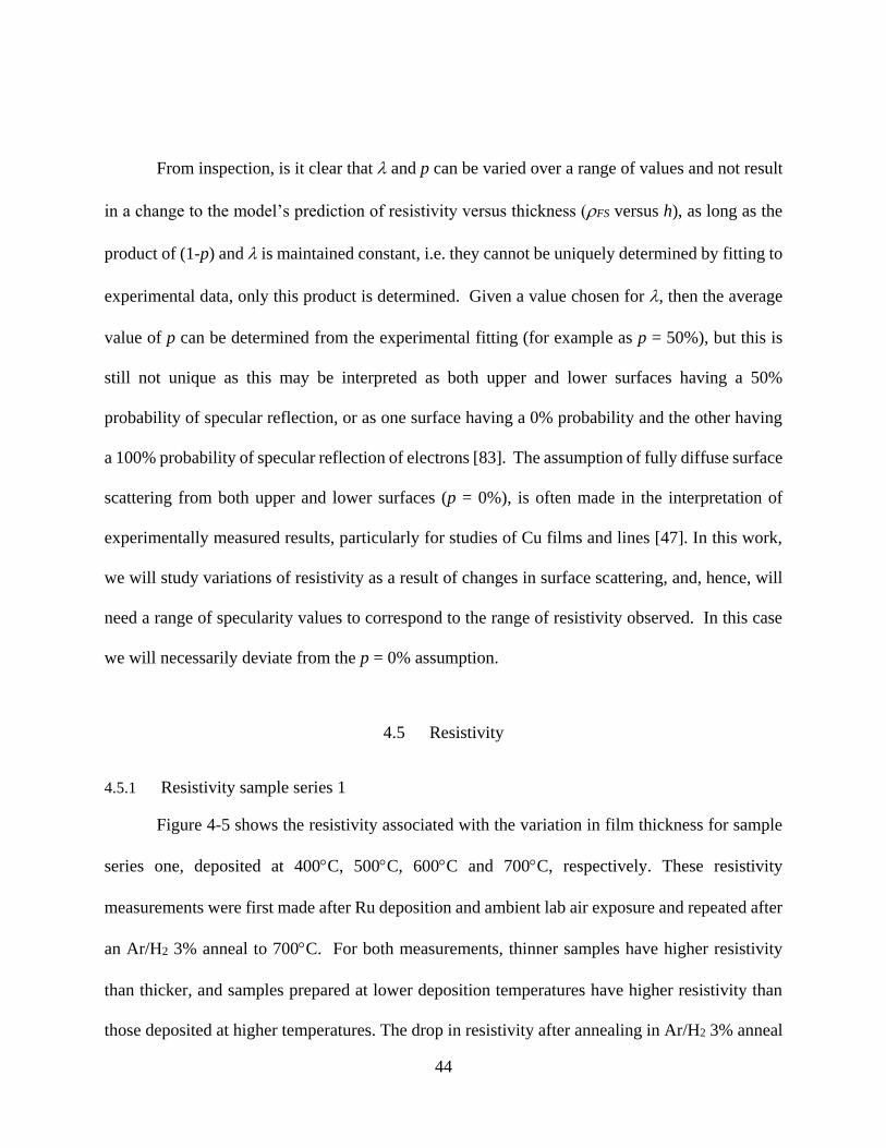
4.5 Resistivity
4.5.1 Resistivity sample series 1
Figure 4-5 shows the resistivity associated with the variation in film thickness for sample
series one, deposited at 400C, 500C, 600C and 700C, respectively. These resistivity
measurements were first made after Ru deposition and ambient lab air exposure and repeated after
an Ar/H2 3% anneal to 700C. For both measurements, thinner samples have higher resistivity
than thicker, and samples prepared at lower deposition temperatures have higher resistivity than
those deposited at higher temperatures. The drop in resistivity after annealing in Ar/H2 3% anneal
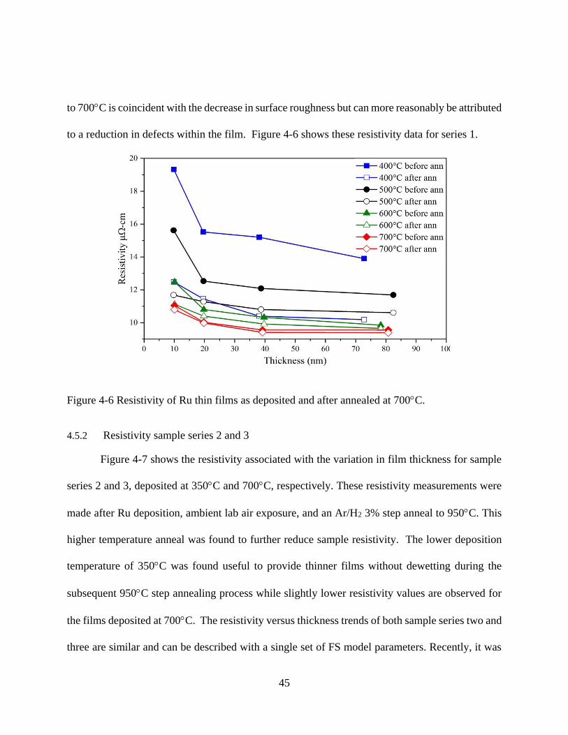
45
to 700C is coincident with the decrease in surface roughness but can more reasonably be attributed
to a reduction in defects within the film. Figure 4-6 shows these resistivity data for series 1.
Figure 4-6 Resistivity of Ru thin films as deposited and after annealed at 700C.
4.5.2 Resistivity sample series 2 and 3
Figure 4-7 shows the resistivity associated with the variation in film thickness for sample
series 2 and 3, deposited at 350C and 700C, respectively. These resistivity measurements were
made after Ru deposition, ambient lab air exposure, and an Ar/H2 3% step anneal to 950C. This
higher temperature anneal was found to further reduce sample resistivity. The lower deposition
temperature of 350C was found useful to provide thinner films without dewetting during the
subsequent 950C step annealing process while slightly lower resistivity values are observed for
the films deposited at 700C. The resistivity versus thickness trends of both sample series two and
three are similar and can be described with a single set of FS model parameters. Recently, it was
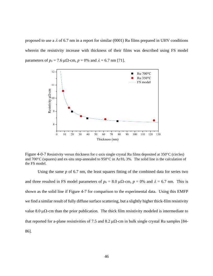
46
proposed to use a of 6.7 nm in a report for similar (0001) Ru films prepared in UHV conditions
wherein the resistivity increase with thickness of their films was described using FS model
parameters of po = 7.6 -cm, p = 0% and = 6.7 nm [71].
Figure 4-0-7 Resistivity versus thickness for c-axis single crystal Ru films deposited at 350C (circles)
and 700C (squares) and ex-situ step-annealed to 950C in Ar/H2 3%. The solid line is the calculation of
the FS model.
Using the same p of 6.7 nm, the least squares fitting of the combined data for series two
and three resulted in FS model parameters of po = 8.0 -cm, p = 0% and = 6.7 nm. This is
shown as the solid line if Figure 4-7 for comparison to the experimental data. Using this EMFP
we find a similar result of fully diffuse surface scattering, but a slightly higher thick-film resistivity
value 8.0 -cm than the prior publication. The thick film resistivity modeled is intermediate to
that reported for a-plane resistivities of 7.5 and 8.2 -cm in bulk single crystal Ru samples [84-
86].

47
4.5.3 Sample series 3
Experimental characterization data of the 8 samples of the third sample series are
summarized in Table 3-3 along with the identification of the process steps after which the data was
taken and the overall sequence of the process steps. A total of 8 samples were annealed together
in a cumulative processing (at different temperatures in 700C in Ar + H2 3%, 950C in Ar + H2
3%, 300C in Ar + H2 3% and air at one atmosphere) and after each process step one sample was
removed from the group for characterization. The resistivity values shown were calculated from
the sheet resistance measured for each sample shown in figure 4-8 and the Ru metal layer thickness
for each sample. The simple trend readily apparent in the table 3-3 is for the resistivity to decrease
as a result of a reducing anneal and to increase as the result of an oxidizing anneal. Figure 4-8
shows the resistivity changes resulting from each processing step.
Figure 4-8 Resistivity of Ru 20 nm thin film during the annealing process
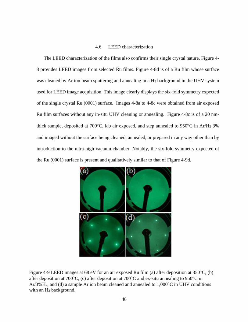
48
4.6 LEED characterization
The LEED characterization of the films also confirms their single crystal nature. Figure 4-
8 provides LEED images from selected Ru films. Figure 4-8d is of a Ru film whose surface
was cleaned by Ar ion beam sputtering and annealing in a H2 background in the UHV system
used for LEED image acquisition. This image clearly displays the six-fold symmetry expected
of the single crystal Ru (0001) surface. Images 4-8a to 4-8c were obtained from air exposed
Ru film surfaces without any in-situ UHV cleaning or annealing. Figure 4-8c is of a 20 nm-
thick sample, deposited at 700C, lab air exposed, and step annealed to 950C in Ar/H2 3%
and imaged without the surface being cleaned, annealed, or prepared in any way other than by
introduction to the ultra-high vacuum chamber. Notably, the six-fold symmetry expected of
the Ru (0001) surface is present and qualitatively similar to that of Figure 4-9d.
Figure 4-9 LEED images at 68 eV for an air exposed Ru film (a) after deposition at 350C, (b)
after deposition at 700C, (c) after deposition at 700C and ex-situ annealing to 950C in
Ar/3%H2, and (d) a sample Ar ion beam cleaned and annealed to 1,000C in UHV conditions
with an H2 background.
49
While it is not clear if the LEED image of Figures 4-9a to 4-9c are the result of low energy
electrons reflecting from the Ru atoms directly, or from an absorbed gas layer on the Ru surface,
it is clear that an ordered surface structure is, surprisingly, observable after the exposure of the Ru
film to ambient air. This also indicates that a relatively well atomically ordered Ru (0001) surface
resulted from the deposition and ex-situ 950C Ar/H2 3% anneal processing of the Ru single crystal
films and that this high degree of atomic surface order persists during laboratory air exposure.
Figures 3a and 3b are from samples as deposited at 350C and 700C, respectively, and imaged
without the 950C Ar/H2 3% anneal. A qualitatively weaker six-fold pattern is present in Figure
4-9b and is essentially absent in Figure 4-9a.
In this dissertation, the additional modifications to the surfaces of samples in series 4, 5,
and 6, prepared identically to those of series 3, result in increases in film resistivity. This cannot
be accommodated by a set of FS model parameters that has the Ru surfaces already fully diffuse
(p = 0%). A larger value is needed to allow variations in specularity (i.e., 100% > p > 0%) while
maintaining the product, (1-p) = 6.7 nm, constant to be consistent with the data and fitting of
Figure 4-7. Table 4-1 lists some of the possible alternative assumptions of FS model parameters
that maintain this product constant. While every set of model parameters shown in Table 4-1 can
equally provide the FS prediction shown in Figure 4-7, we choose to use the set of o = 8.0 -
cm, = 11 nm, and pl = 0% and pu = 78% as these provide for variations of resistivity associated
with changes to the upper Ru surface while avoiding large values for the that are inconsistent
with the previous work.
The high specularity pu = 78%, of the air-exposed Ru surface is surprising in light of prior
UHV experiments for single crystal Ni and Cu surfaces where ambient air and sub-monolayer gas
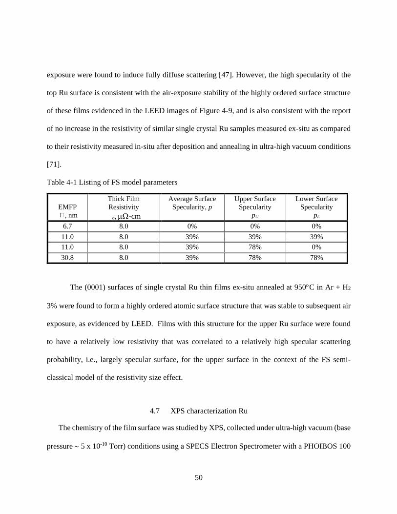
50
exposure were found to induce fully diffuse scattering [47]. However, the high specularity of the
top Ru surface is consistent with the air-exposure stability of the highly ordered surface structure
of these films evidenced in the LEED images of Figure 4-9, and is also consistent with the report
of no increase in the resistivity of similar single crystal Ru samples measured ex-situ as compared
to their resistivity measured in-situ after deposition and annealing in ultra-high vacuum conditions
[71].
Table 4-1 Listing of FS model parameters
EMFP
, nm
Thick Film
Resistivity
o, -cm
Average Surface
Specularity, p
Upper Surface
Specularity
pU
Lower Surface
Specularity
pL
6.7 8.0 0% 0% 0%
11.0 8.0 39% 39% 39%
11.0 8.0 39% 78% 0%
30.8 8.0 39% 78% 78%
The (0001) surfaces of single crystal Ru thin films ex-situ annealed at 950C in Ar + H2
3% were found to form a highly ordered atomic surface structure that was stable to subsequent air
exposure, as evidenced by LEED. Films with this structure for the upper Ru surface were found
to have a relatively low resistivity that was correlated to a relatively high specular scattering
probability, i.e., largely specular surface, for the upper surface in the context of the FS semi-
classical model of the resistivity size effect.
4.7 XPS characterization Ru
The chemistry of the film surface was studied by XPS, collected under ultra-high vacuum (base
pressure 5 x 10⁻¹⁰ Torr) conditions using a SPECS Electron Spectrometer with a PHOIBOS 100

51
Hemispherical Energy Analyzer and XR 50 Al K X-ray source (1486.67 eV). The XPS spectra
were collected at a pass energy of 20 eV with energy resolution of 0.1 eV. The XPS spectra were
fitted using XPSPEAK 4.1 program with Gaussian/Lorentzian mixed peak shape and with Shirley
background correction. The normalized Ru 3d5/2 peak heights allowed interpretation by fitting to
two components, Ru0 and oxidized Ruδ+, at binding energies (BEs) consistent with metallic Ru
and RuO2, respectively. In addition, C 1s features have also been included as needed to fit the data.
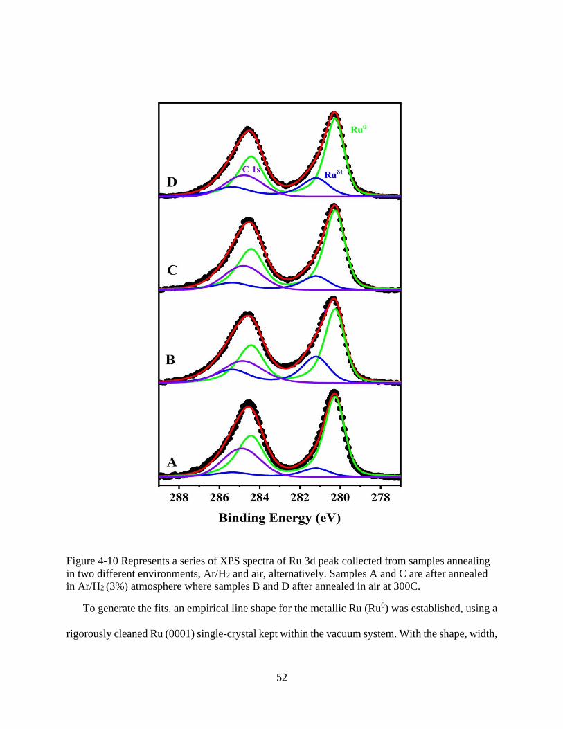
52
Figure 4-10 Represents a series of XPS spectra of Ru 3d peak collected from samples annealing
in two different environments, Ar/H2 and air, alternatively. Samples A and C are after annealed
in Ar/H2 (3%) atmosphere where samples B and D after annealed in air at 300C.
To generate the fits, an empirical line shape for the metallic Ru (Ru0) was established, using a
rigorously cleaned Ru (0001) single-crystal kept within the vacuum system. With the shape, width,
53
and position of this peak constrained to fixed values equivalent to those from the control sample,
a second peak associated with RuO2 (Ruδ+) was added to the experimental spectra of each sample
as needed to ensure proper fitting of the 5/2 spin-orbit splitting components, where the C 1s signal
is not expected to contribute to the XPS intensity. With the 5/2 component fit as well as possible
by the two features associated with oxidized and unoxidized Ru, residual differences between the
data and the fitting in the Ru 3d 3/2 component region of the spectra, the higher binding energy
(BE) feature present in each, were fit to a single unconstrained C 1s peak. From XPS spectra it is
clear that the oxide component (Ruδ+) of Ru 3d increased after annealing in air (Figure 4-9b, and
4-9d) and it decreases in more reducing environment (Ar/H2).
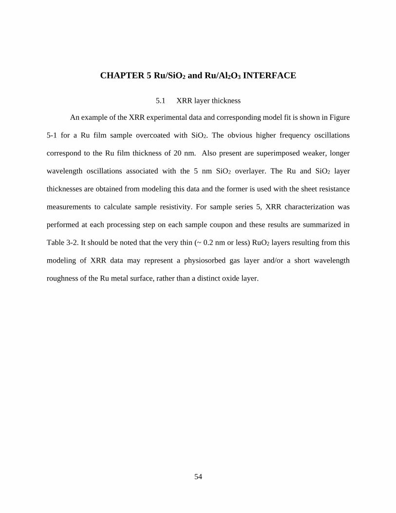
54
CHAPTER 5 Ru/SiO2 and Ru/Al2O3 INTERFACE
5.1 XRR layer thickness
An example of the XRR experimental data and corresponding model fit is shown in Figure
5-1 for a Ru film sample overcoated with SiO2. The obvious higher frequency oscillations
correspond to the Ru film thickness of 20 nm. Also present are superimposed weaker, longer
wavelength oscillations associated with the 5 nm SiO2 overlayer. The Ru and SiO2 layer
thicknesses are obtained from modeling this data and the former is used with the sheet resistance
measurements to calculate sample resistivity. For sample series 5, XRR characterization was
performed at each processing step on each sample coupon and these results are summarized in
Table 3-2. It should be noted that the very thin (~ 0.2 nm or less) RuO2 layers resulting from this
modeling of XRR data may represent a physiosorbed gas layer and/or a short wavelength
roughness of the Ru metal surface, rather than a distinct oxide layer.
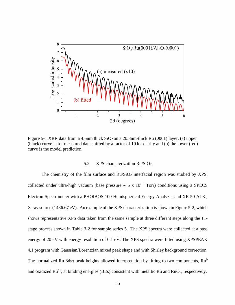
55
Figure 5-1 XRR data from a 4.6nm thick SiO2 on a 20.8nm-thick Ru (0001) layer. (a) upper
(black) curve is for measured data shifted by a factor of 10 for clarity and (b) the lower (red)
curve is the model prediction.
5.2 XPS characterization Ru/SiO2
The chemistry of the film surface and Ru/SiO2 interfacial region was studied by XPS,
collected under ultra-high vacuum (base pressure 5 x 10⁻¹⁰ Torr) conditions using a SPECS
Electron Spectrometer with a PHOIBOS 100 Hemispherical Energy Analyzer and XR 50 Al K
X-ray source (1486.67 eV). An example of the XPS characterization is shown in Figure 5-2, which
shows representative XPS data taken from the same sample at three different steps along the 11-
stage process shown in Table 3-2 for sample series 5. The XPS spectra were collected at a pass
energy of 20 eV with energy resolution of 0.1 eV. The XPS spectra were fitted using XPSPEAK
4.1 program with Gaussian/Lorentzian mixed peak shape and with Shirley background correction.
The normalized Ru 3d5/2 peak heights allowed interpretation by fitting to two components, Ru0
and oxidized Ruδ+, at binding energies (BEs) consistent with metallic Ru and RuO2, respectively.
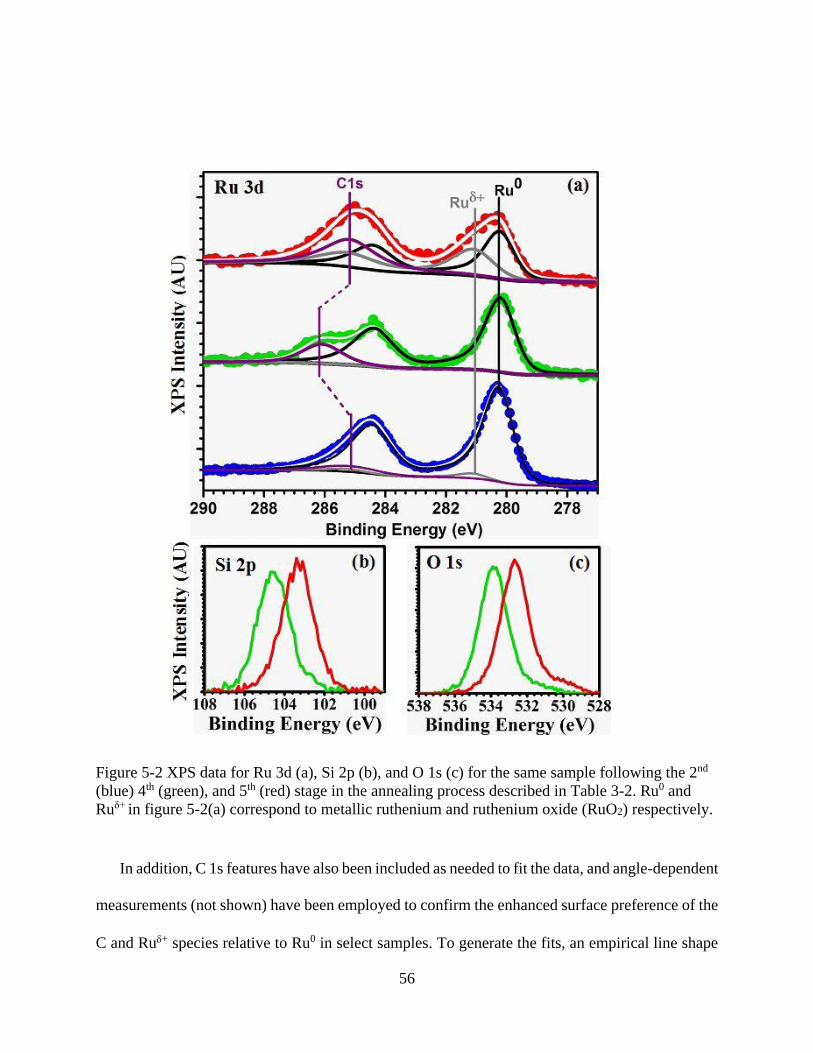
56
Figure 5-2 XPS data for Ru 3d (a), Si 2p (b), and O 1s (c) for the same sample following the 2nd
(blue) 4th (green), and 5th (red) stage in the annealing process described in Table 3-2. Ru0 and
Ruδ+ in figure 5-2(a) correspond to metallic ruthenium and ruthenium oxide (RuO2) respectively.
In addition, C 1s features have also been included as needed to fit the data, and angle-dependent
measurements (not shown) have been employed to confirm the enhanced surface preference of the
C and Ru+ species relative to Ru0 in select samples. To generate the fits, an empirical line shape
57
for the metallic Ru (Ru0) was established, using a rigorously cleaned Ru (0001) single-crystal kept
within the vacuum system. With the shape, width, and position of this peak constrained to fixed
values equivalent to those from the control sample, a second peak associated with RuO2 (Ruδ+)
was added to the experimental spectra of each sample as needed to ensure proper fitting of the 5/2
spin-orbit splitting components, where the C 1s signal is not expected to contribute to the XPS
intensity. With the 5/2 component fit as well as possible by the two features associated with
oxidized and unoxidized Ru, residual differences between the data and the fitting in the Ru 3d 3/2
component region of the spectra, the higher binding energy (BE) feature present in each, were fit
to a single unconstrained C 1s peak.
Noting large variations in both the position and intensity of the C 1s features needed to
accurately fit our data as a function of condition, we obtained XPS spectra associated with step 7
for two samples exposed to air for drastically different periods of time between annealing and
vacuum introduction, which was an uncontrolled (but measured) variable throughout the
remainder of the data set. This variable results in clear changes to the amount of C detected by
XPS, but does not result in changes to the Ruδ+:Ru0 XPS intensity ratio. To provide further insight
into the nature of the spurious carbon species on the samples, we also provide O 1s and Si 2p
regional XPS plots from the 4th and 5th process steps in Figure 5-2. Interestingly, the same ~1 eV
shift to lower binding energy (BE) noted for the C 1s contribution to the Ru 3d region is also noted
in both the O 1s and Si 2p data when transitioning from step 4 (Ar/H2 annealing) to step 5 (air
annealing) in our multi-step process sequence. This combination of data is consistent with carbon
on or within the SiO2 layer present at the interface of Ru undergoing changes in work-function as
the interfacial oxidation state of the metal transitions from Ru to RuO2, which then results in
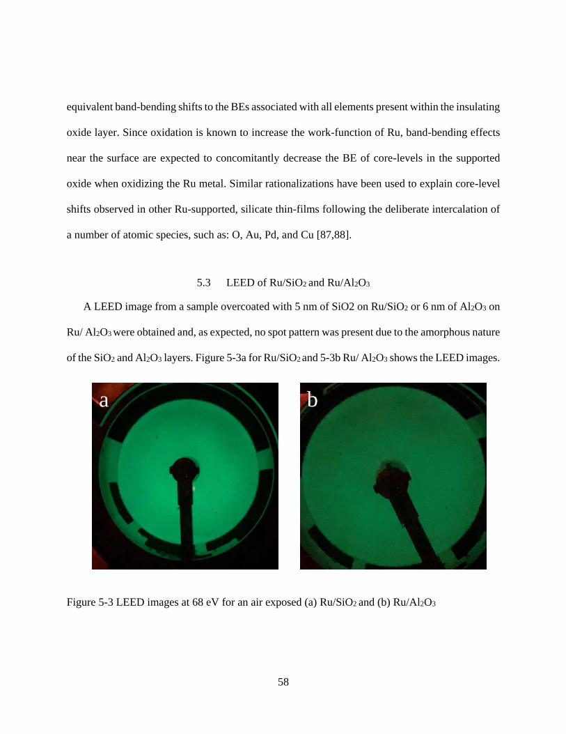
58
equivalent band-bending shifts to the BEs associated with all elements present within the insulating
oxide layer. Since oxidation is known to increase the work-function of Ru, band-bending effects
near the surface are expected to concomitantly decrease the BE of core-levels in the supported
oxide when oxidizing the Ru metal. Similar rationalizations have been used to explain core-level
shifts observed in other Ru-supported, silicate thin-films following the deliberate intercalation of
a number of atomic species, such as: O, Au, Pd, and Cu [87,88].
5.3 LEED of Ru/SiO2 and Ru/Al2O3
A LEED image from a sample overcoated with 5 nm of SiO2 on Ru/SiO2 or 6 nm of Al2O3 on
Ru/ Al2O3 were obtained and, as expected, no spot pattern was present due to the amorphous nature
of the SiO2 and Al2O3 layers. Figure 5-3a for Ru/SiO2 and 5-3b Ru/ Al2O3 shows the LEED images.
Figure 5-3 LEED images at 68 eV for an air exposed (a) Ru/SiO2 and (b) Ru/Al2O3
a b
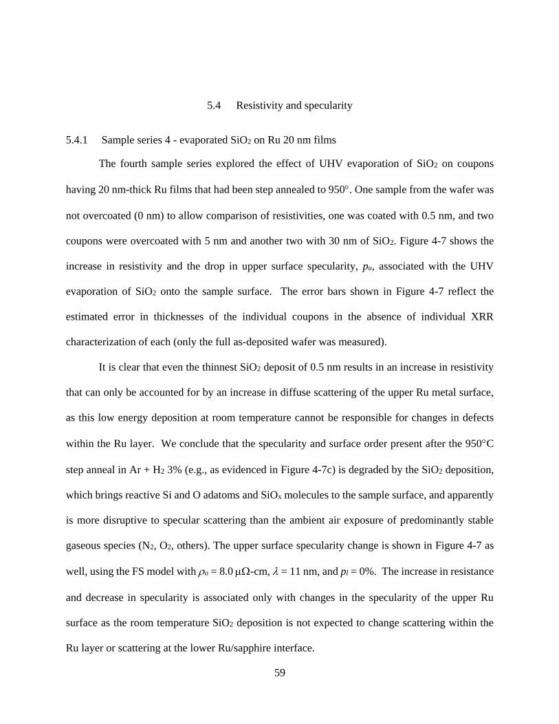
59
5.4 Resistivity and specularity
5.4.1 Sample series 4 - evaporated SiO2 on Ru 20 nm films
The fourth sample series explored the effect of UHV evaporation of SiO2 on coupons
having 20 nm-thick Ru films that had been step annealed to 950. One sample from the wafer was
not overcoated (0 nm) to allow comparison of resistivities, one was coated with 0.5 nm, and two
coupons were overcoated with 5 nm and another two with 30 nm of SiO2. Figure 4-7 shows the
increase in resistivity and the drop in upper surface specularity, pu, associated with the UHV
evaporation of SiO2 onto the sample surface. The error bars shown in Figure 4-7 reflect the
estimated error in thicknesses of the individual coupons in the absence of individual XRR
characterization of each (only the full as-deposited wafer was measured).
It is clear that even the thinnest SiO2 deposit of 0.5 nm results in an increase in resistivity
that can only be accounted for by an increase in diffuse scattering of the upper Ru metal surface,
as this low energy deposition at room temperature cannot be responsible for changes in defects
within the Ru layer. We conclude that the specularity and surface order present after the 950C
step anneal in Ar + H2 3% (e.g., as evidenced in Figure 4-7c) is degraded by the SiO2 deposition,
which brings reactive Si and O adatoms and SiOx molecules to the sample surface, and apparently
is more disruptive to specular scattering than the ambient air exposure of predominantly stable
gaseous species (N2, O2, others). The upper surface specularity change is shown in Figure 4-7 as
well, using the FS model with o = 8.0 -cm, = 11 nm, and pl = 0%. The increase in resistance
and decrease in specularity is associated only with changes in the specularity of the upper Ru
surface as the room temperature SiO2 deposition is not expected to change scattering within the
Ru layer or scattering at the lower Ru/sapphire interface.
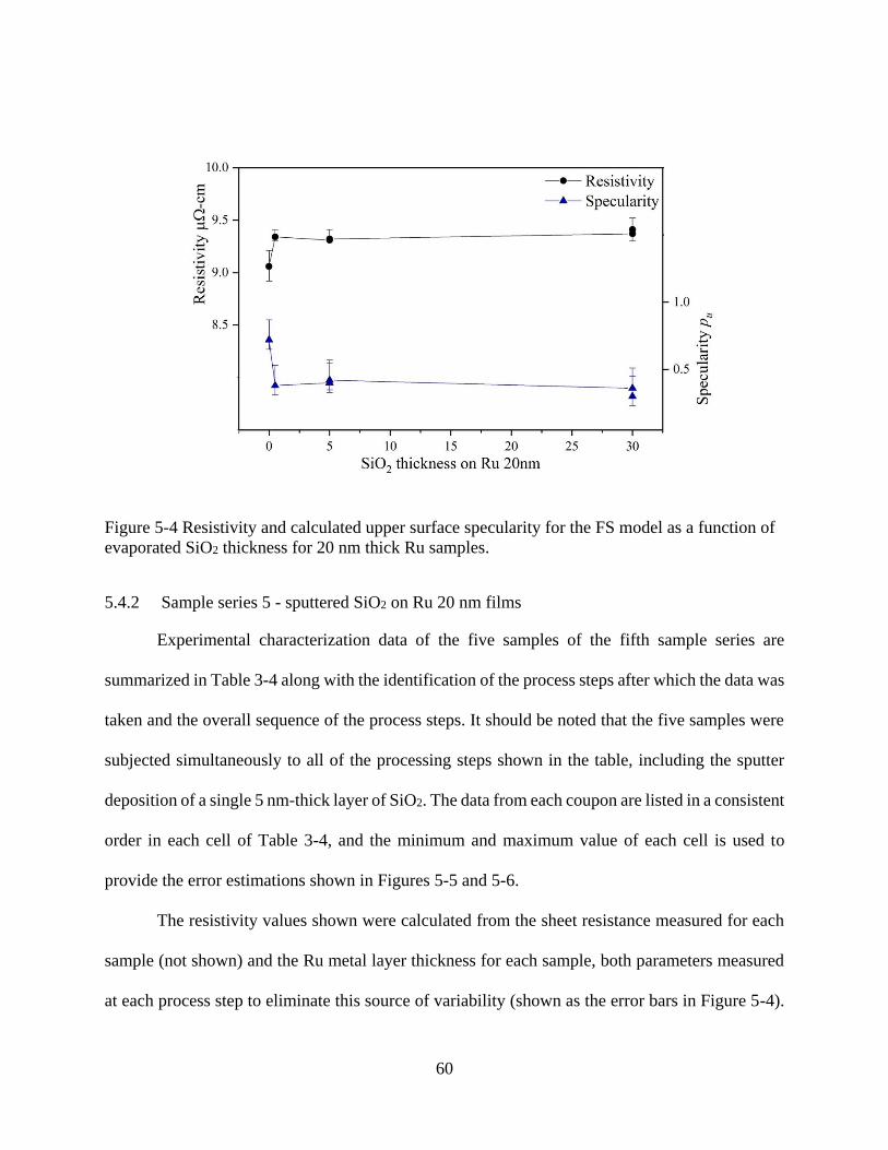
60
Figure 5-4 Resistivity and calculated upper surface specularity for the FS model as a function of
evaporated SiO2 thickness for 20 nm thick Ru samples.
5.4.2 Sample series 5 - sputtered SiO2 on Ru 20 nm films
Experimental characterization data of the five samples of the fifth sample series are
summarized in Table 3-4 along with the identification of the process steps after which the data was
taken and the overall sequence of the process steps. It should be noted that the five samples were
subjected simultaneously to all of the processing steps shown in the table, including the sputter
deposition of a single 5 nm-thick layer of SiO2. The data from each coupon are listed in a consistent
order in each cell of Table 3-4, and the minimum and maximum value of each cell is used to
provide the error estimations shown in Figures 5-5 and 5-6.
The resistivity values shown were calculated from the sheet resistance measured for each
sample (not shown) and the Ru metal layer thickness for each sample, both parameters measured
at each process step to eliminate this source of variability (shown as the error bars in Figure 5-4).
61
The simple trend readily apparent in the table is for the resistivity to decrease as a result of a
reducing anneal and to increase as a result of the SiO2 overlayer deposition or as the result of an
oxidizing anneal.
Figure 5-5 Film resistivity and FS model upper surface specularity (pu) as a function of sample
processing. Shown are average values for the five samples with error bars to reflect the extreme
values amongst the five.
Figure 5-6 shows the resistivity changes (left-hand axis) resulting from each processing
step. Also observed here is the increase in resistivity resulting from the deposition of an amorphous
5 nm-thick SiO2 overlayer on top of the Ru films that had been previously step annealed to 950C
in Ar + H2 3%. As above, these resistivity changes are described by the FS model with o = 8.0
-cm, = 11 nm, and pl = 0%. As with sample series 4, an increase in surface roughness, a
change in defect-related scattering within the layer, or a change in the lower Ru/sapphire interface
cannot be expected from the room temperature SiO2 overlayer deposition. The addition of the
amorphous overlayer is understood to have increased surface scattering of the upper Ru surface,
by an increase in the diffuse scattering fraction, from a surface that was largely specular. This

62
increase in diffuse scattering can be understood as resulting from localized surface states that
scatter electrons [44,47]. These states are likely associated with atomic scale defects and/or the
irregular bonding of Si and O adatoms and SiOx molecules at the Ru metal surface. The variations
of the specularity of the upper surface are also shown in Figure 5-6 using the right-hand axis and
exhibit a variation in specularity of approximately 60%. Figure 5-6 plots the average value and
presents the minimum and maximum values of the five samples as errors bars. It is evident that
the difference between the maximum and minimum values in resistivity (and hence specularity)
tends to increase with additional processing steps. We attribute this to the physical damage (i.e.,
scratches) imparted by the repeated probing of the sample surface by the sharp W wire contacts
for the Van der Pauw sheet resistance measurements.
Figure 5-6 summarizes the trend of several of the measured sample characteristics from
Table 3-4 as a function of processing step and compares these to the changes in FS model
specularity. Shown are the changes in the Ru metal layer thickness (from the as-deposited state),
the RuO2 layer thickness, the XPS Ru+/Ru0 ratio, the Ru upper surface roughness, and the
calculated specularity. It is evident that the oxidizing anneals, steps 5 and 8, at 500C and 400C
respectively, provided a significant increase in the RuO2 thickness with corresponding decreases
in the Ru metal thickness that are consistent with the expected variations in stoichiometry and
density in the two layers. A much weaker effect was observed for step 10, an oxidizing anneal at
350C. The higher temperature oxidizing anneals also destroyed the relatively specular scattering
of the Ru upper surface to values similar to that immediately following SiO2 overlayer deposition.

63
Figure 5-6 Shows (a) Ru metal thickness change, (b) RuOx, (c) Ru oxide to Ru metal ratio, (d)
Ru roughness and (e) surface specularity (p) processing as a function of sample shown are
average values for the five samples with error bars to reflect the extreme values amongst the five.
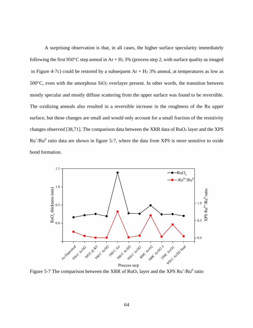
64
A surprising observation is that, in all cases, the higher surface specularity immediately
following the first 950C step anneal in Ar + H2 3% (process step 2, with surface quality as imaged
in Figure 4-7c) could be restored by a subsequent Ar + H2 3% anneal, at temperatures as low as
500C, even with the amorphous SiO2 overlayer present. In other words, the transition between
mostly specular and mostly diffuse scattering from the upper surface was found to be reversible.
The oxidizing anneals also resulted in a reversible increase in the roughness of the Ru upper
surface, but these changes are small and would only account for a small fraction of the resistivity
changes observed [38,71]. The comparison data between the XRR data of RuOx layer and the XPS
Ru+/Ru0 ratio data are shown in figure 5-7, where the data from XPS is more sensitive to oxide
bond formation.
Figure 5-7 The comparison between the XRR of RuOx layer and the XPS Ru+/Ru0 ratio
65
5.4.3 Samples series 6 - Sputtered Al2O3 on Ru 20 nm films
The summary of the three samples of the sixth sample series are in Table 3-5 along with
the identification of the process steps after which the data was taken and the overall sequence of
the process steps. It should be noted that the three samples were subjected simultaneously to all of
the processing steps shown in the table, including the sputter deposition of a single 6 nm-thick
layer of Al2O3. The data from each coupon are listed in a consistent order in each cell of Table 3-
5.
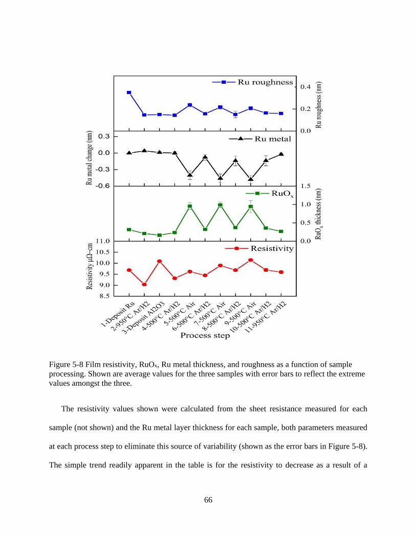
66
Figure 5-8 Film resistivity, RuOx, Ru metal thickness, and roughness as a function of sample
processing. Shown are average values for the three samples with error bars to reflect the extreme
values amongst the three.
The resistivity values shown were calculated from the sheet resistance measured for each
sample (not shown) and the Ru metal layer thickness for each sample, both parameters measured
at each process step to eliminate this source of variability (shown as the error bars in Figure 5-8).
The simple trend readily apparent in the table is for the resistivity to decrease as a result of a

67
reducing anneal and to increase as a result of the Al2O3 overlayer deposition or as the result of an
oxidizing anneal.
Steps 5, 7, and 9, at 500C provided a significant increase in the RuO2 thickness with
corresponding decreases in the Ru metal thickness that are consistent with the expected variations
in stoichiometry and density in the two layers. The last anneal at 950C in Ar + H2 3% decreased
the resistivity but not to the same extent as for sample series 5 where the anneal at 950C in Ar +
H2 3% restored the samples to the initial low resistivity condition. Sample series 6 (Ru/Al2O3)
exhibited and even greater difference between maximum and minimum resistivity and was not fit
to an FS model because of the large value of this would have required.

68
CHAPTER 6 RUTHENIUM ON (1𝟏0), (100), (102), and (104)
SAPPHIRE
6.1 Introduction
Single crystal thin films of ruthenium on oxide substrates are expected to be important to
future semiconductor interconnect technology due to its relatively lower resistivity and high
melting temperature. Ruthenium has a hexagonal close-packed (hcp) crystal structure and even in
bulk form has a lower electrical resistivity for current directed parallel to the crystallographic c-
axis than for current in directions perpendicular to the c-axis. Of specific interest is that
crystallographic planes perpendicular to the c-axis have lower surface energy and the electric
current flowing parallel to the c-axis has lower resistivity The prior work allowed the formation of
single crystal Ru films with the c-axis perpendicular to the film layer, which resulted in only the
higher resistivity directions available for nanowire semiconductor interconnects. The structure that
attempt to grow is a single crystal Ru film on an insulating substrate that has the c-axis in the plane,
this will allow a significant reduction in the resistance of Ru when used for semiconductor
interconnect nanowires. The Ru thin films were deposited on different sapphire substrate such as
sapphire (1120), (1010), (1012), and (1014) substrate. These depositions were an attempt to grow
a single crystal c-axis in the plane on these sapphire substrates.
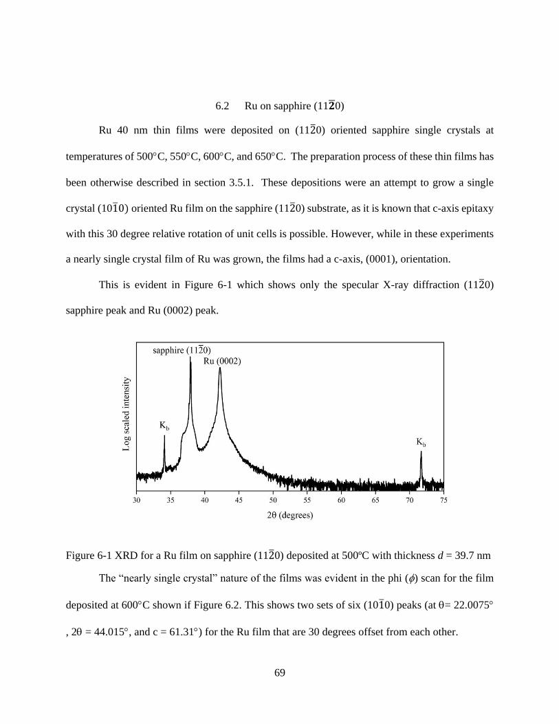
69
6.2 Ru on sapphire (110)
Ru 40 nm thin films were deposited on (1120) oriented sapphire single crystals at
temperatures of 500C, 550C, 600C, and 650C. The preparation process of these thin films has
been otherwise described in section 3.5.1. These depositions were an attempt to grow a single
crystal (1010) oriented Ru film on the sapphire (1120) substrate, as it is known that c-axis epitaxy
with this 30 degree relative rotation of unit cells is possible. However, while in these experiments
a nearly single crystal film of Ru was grown, the films had a c-axis, (0001), orientation.
This is evident in Figure 6-1 which shows only the specular X-ray diffraction (1120)
sapphire peak and Ru (0002) peak.
Figure 6-1 XRD for a Ru film on sapphire (1120) deposited at 500ºC with thickness d = 39.7 nm
The “nearly single crystal” nature of the films was evident in the phi () scan for the film
deposited at 600C shown if Figure 6.2. This shows two sets of six (1010) peaks (at = 22.0075
, 2 = 44.015, and c = 61.31) for the Ru film that are 30 degrees offset from each other.
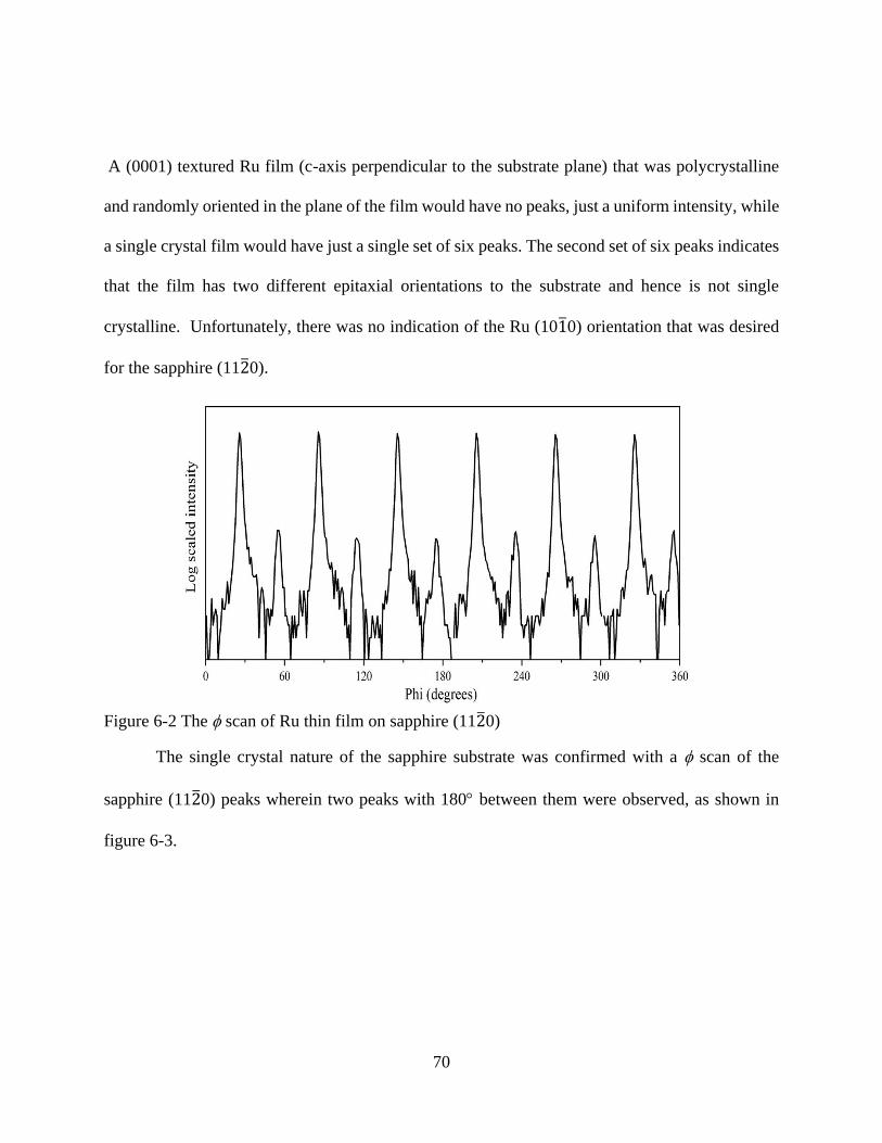
70
A (0001) textured Ru film (c-axis perpendicular to the substrate plane) that was polycrystalline
and randomly oriented in the plane of the film would have no peaks, just a uniform intensity, while
a single crystal film would have just a single set of six peaks. The second set of six peaks indicates
that the film has two different epitaxial orientations to the substrate and hence is not single
crystalline. Unfortunately, there was no indication of the Ru (1010) orientation that was desired
for the sapphire (1120).
Figure 6-2 The scan of Ru thin film on sapphire (1120)
The single crystal nature of the sapphire substrate was confirmed with a scan of the
sapphire (1120) peaks wherein two peaks with 180 between them were observed, as shown in
figure 6-3.
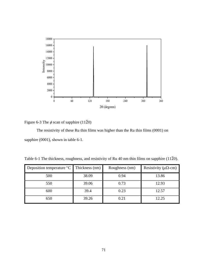
71
Figure 6-3 The scan of sapphire (1120)
The resistivity of these Ru thin films was higher than the Ru thin films (0001) on
sapphire (0001), shown in table 6-1.
Table 6-1 The thickness, roughness, and resistivity of Ru 40 nm thin films on sapphire (1120).
Deposition temperature C Thickness (nm) Roughness (nm) Resistivity (-cm)
500 38.09 0.94 13.86
550 39.06 0.73 12.93
600 39.4 0.23 12.57
650 39.26 0.21 12.25
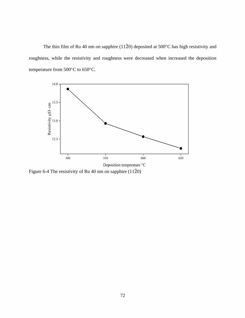
72
The thin film of Ru 40 nm on sapphire (1120) deposited at 500C has high resistivity and
roughness, while the resistivity and roughness were decreased when increased the deposition
temperature from 500C to 650C.
Figure 6-4 The resistivity of Ru 40 nm on sapphire (1120)
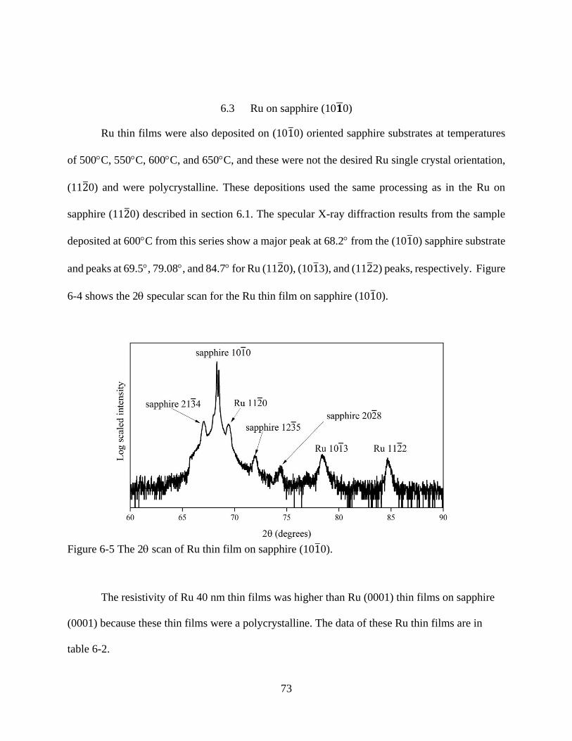
73
6.3 Ru on sapphire (100)
Ru thin films were also deposited on (1010) oriented sapphire substrates at temperatures
of 500C, 550C, 600C, and 650C, and these were not the desired Ru single crystal orientation,
(1120) and were polycrystalline. These depositions used the same processing as in the Ru on
sapphire (1120) described in section 6.1. The specular X-ray diffraction results from the sample
deposited at 600C from this series show a major peak at 68.2 from the (1010) sapphire substrate
and peaks at 69.5, 79.08, and 84.7 for Ru (1120), (1013), and (1122) peaks, respectively. Figure
6-4 shows the 2 specular scan for the Ru thin film on sapphire (1010).
Figure 6-5 The 2 scan of Ru thin film on sapphire (1010).
The resistivity of Ru 40 nm thin films was higher than Ru (0001) thin films on sapphire
(0001) because these thin films were a polycrystalline. The data of these Ru thin films are in
table 6-2.

74
Table 6-2 The thickness, roughness, and resistivity of Ru 40 nm thin films on sapphire (1010).
Deposition temperature C Thickness (nm) Roughness (nm) Resistivity (-cm)
500 39.7753 1.27 13.01
550 39.1332 0.62 12.56
600 39.502 0.5 12.36
650 40.4996 0.48 12.07
The thin film of Ru 40 nm on sapphire (1010) deposited at 500C has low resistivity and
roughness than the resistivity of Ru thin film on sapphire (1120) deposited at 500C. Where the
resistivity and roughness were decreased also when increased the deposition temperature from
500C to 650C.
Figure 6-6 The resistivity of Ru 40 nm on sapphire (1010)
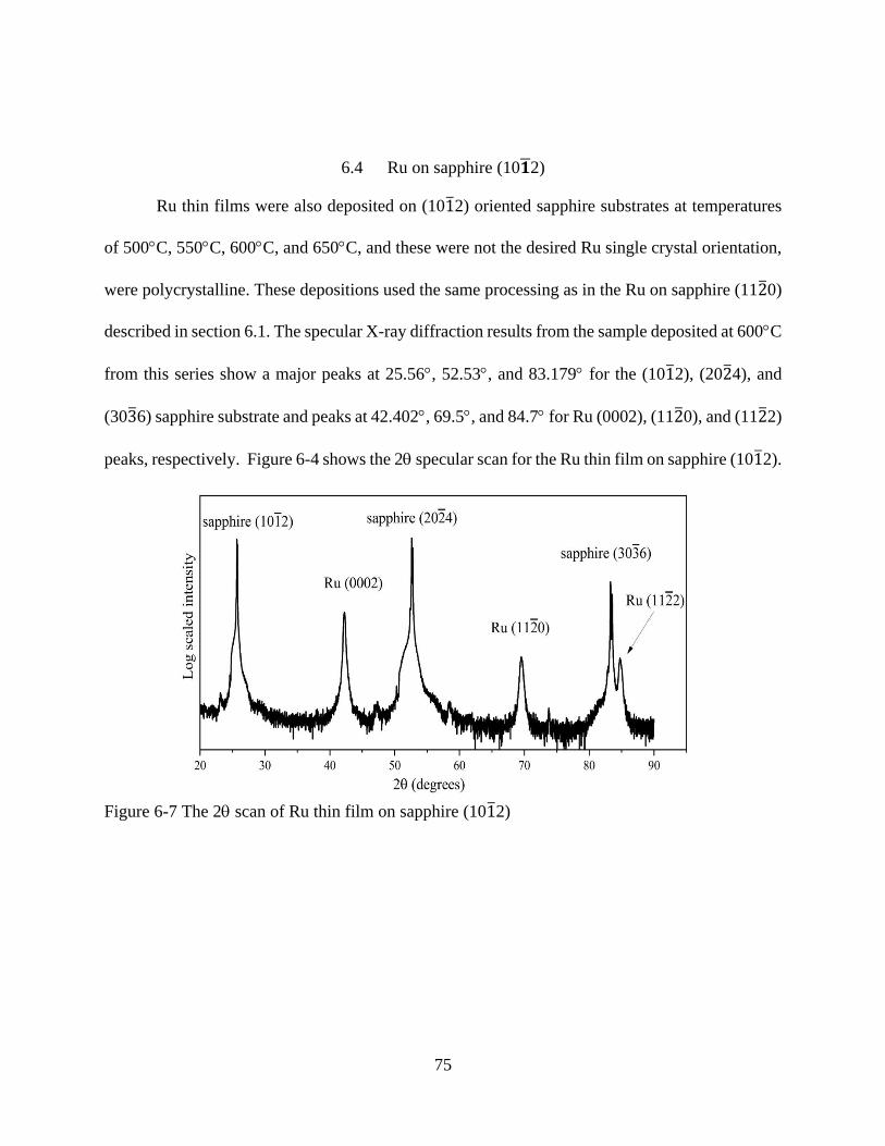
75
6.4 Ru on sapphire (102)
Ru thin films were also deposited on (1012) oriented sapphire substrates at temperatures
of 500C, 550C, 600C, and 650C, and these were not the desired Ru single crystal orientation,
were polycrystalline. These depositions used the same processing as in the Ru on sapphire (1120)
described in section 6.1. The specular X-ray diffraction results from the sample deposited at 600C
from this series show a major peaks at 25.56, 52.53, and 83.179 for the (1012), (2024), and
(3036) sapphire substrate and peaks at 42.402, 69.5, and 84.7 for Ru (0002), (1120), and (1122)
peaks, respectively. Figure 6-4 shows the 2 specular scan for the Ru thin film on sapphire (1012).
Figure 6-7 The 2 scan of Ru thin film on sapphire (1012)
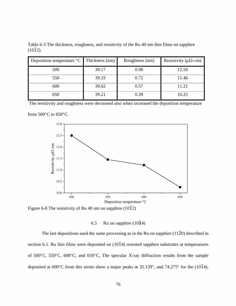
76
Table 6-3 The thickness, roughness, and resistivity of the Ru 40 nm thin films on sapphire
(1012).
Deposition temperature C Thickness (nm) Roughness (nm) Resistivity (-cm)
500 39.17 0.98 12.50
550 39.33 0.72 11.46
600 39.62 0.57 11.21
650 39.21 0.39 10.25
The resistivity and roughness were decreased also when increased the deposition temperature
from 500C to 650C.
Figure 6-8 The resistivity of Ru 40 nm on sapphire (1012)
6.5 Ru on sapphire (104)
The last depositions used the same processing as in the Ru on sapphire (1120) described in
section 6.1. Ru thin films were deposited on (1014) oriented sapphire substrates at temperatures
of 500C, 550C, 600C, and 650C, The specular X-ray diffraction results from the sample
deposited at 600C from this series show a major peaks at 35.139, and 74.275 for the (1014),

77
and (2028), sapphire substrate and peaks at 42.402, and 92.093 for Ru (0002), and (0004) peaks,
respectively. Figure 6-9 shows the 2 specular scan for the Ru thin film on sapphire (1014)
Figure 6-9 The 2 scan of Ru thin film on sapphire (1014)
The resistivity of Ru thin films was higher than the other Ru thin films on (1120), (1010),
and (1012) sapphire substrates, even the Ru thin film that deposited at 650C.
Table 6-4 The thickness, roughness, and resistivity of Ru 40 nm thin films on sapphire (1014).
Deposition temperature C Thickness (nm) Roughness (nm) Resistivity (-cm)
500 39.14 0.95 15.73
550 39.42 0.71 15.61
600 39.81 0.63 15.25
650 39.28 0.44 13.98
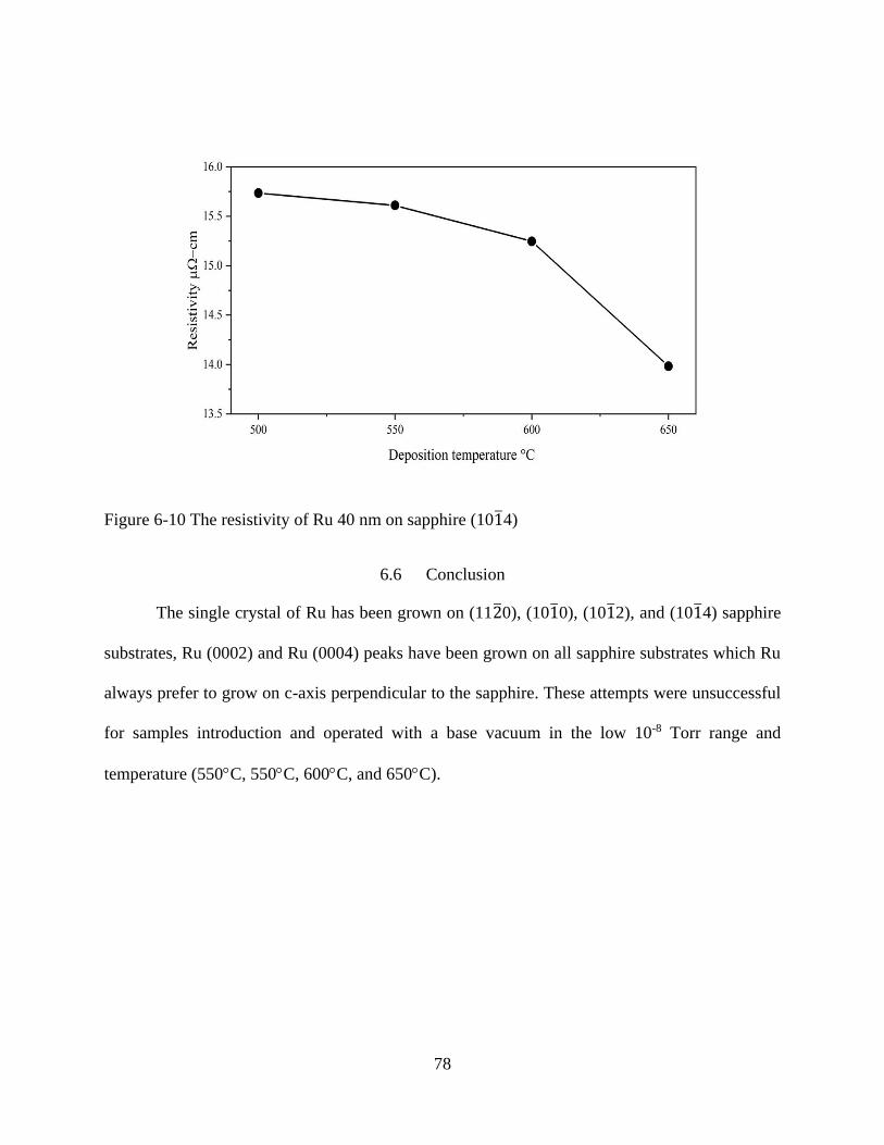
78
Figure 6-10 The resistivity of Ru 40 nm on sapphire (1014)
6.6 Conclusion
The single crystal of Ru has been grown on (1120), (1010), (1012), and (1014) sapphire
substrates, Ru (0002) and Ru (0004) peaks have been grown on all sapphire substrates which Ru
always prefer to grow on c-axis perpendicular to the sapphire. These attempts were unsuccessful
for samples introduction and operated with a base vacuum in the low 10-8 Torr range and
temperature (550C, 550C, 600C, and 650C).
79
CHAPTER 7 SUMMARY
Ru thin films on c-plane sapphire substrates have been grown by sputter deposition. The
films were found to be epitaxial with a 30 offset in the phi positions of these peaks observed, as
expected for the 30 rotational honeycomb epitaxial relationship of (0001) Ru || (0001) sapphire
and <1120>Ru ||<1010> sapphire. The resistivity of the Ru thin films showed dependence on
processing, where the samples annealed at 700C in Ar + H2 3% (series 1) had higher resistivity
than the samples that annealed at 950C Ar + H2 3% (series 2 and 3). The Ru surface roughness
decreased after annealing in both cases. The resistivity versus thickness trends of sample series
two and three are similar and can be described with a single set of FS model parameters. Using
the same EMFP of 6.7 nm, the least squares fitting of the combined data for series two and three
resulted in FS model parameters of o = 8.0 -cm and p = 0% (fully diffuse surface scattering).
Alternatively, the data can be equally well by a EMFP of 11 nm and p = 39% (mostly specular
surface scattering) with the same o = 8.0 -cm. This is shown as the solid line in Figure 4-6
for comparison to the experimental data. This thick film resistivity (o) is intermediate to that
reported for a-plane resistivities of 7.5 and 8.2 -cm in bulk single crystal Ru samples
The deposition of SiO2 on this surface, by sputtering or evaporation, was found to increase
the resistivity and reduce the specularity of the surface. A subsequent anneal at 500C in Ar + H2
3% was found to restore the low resistivity and high specularity of the upper surface. Subsequent
oxidizing anneals at 500C and 400C were again found to reduce the specularity of the upper
surface while intermediate Ar + H2 3% anneals were found to restore it. For the 20 nm thick Ru
(0001) single crystal films, the relatively low and high specular scattering probabilities for the
80
upper Ru surface were found to differ in magnitude by approximately 60% and to be substantially
reversible.
The deposition of Al2O3 on the Ru 20nm surface, by sputtering, was found to also increase
the resistivity and reduce the specularity of the surface as a SiO2. A subsequent anneal at 500C in
Ar + H2 3% was found to restore the low resistivity and high specularity of the upper surface.
Subsequent oxidizing anneals at 500C was again found to reduce the specularity of the upper
surface while intermediate Ar + H2 3% anneals were found to restore some, where the resistivity
was still higher than the Ru/SiO2 after annealed at 950C in Ar + H2 3%.
The observation of surface specularity (sample series 3) greater than 60% is novel for a
film surface not in UHV conditions. That this observation occurred for a buried metal/dielectric
interface is a very significant and promising development for microelectronics, wherein all the
interconnect wires are encased in dielectric and the surface scattering of these fully diffuse wire
surfaces is currently limiting microprocessor speeds and consuming a majority of the electrical
power.
81
CHAPTER 8 FUTURE WORK
8.1 Deposit Ru thin film on sapphire (110) and sapphire (100)
Ruthenium has a hexagonal close-packed (hcp) crystal structure and even in bulk form has
a lower electrical resistivity for current directed parallel to the crystallographic c-axis than for
current in directions perpendicular to the c-axis. Of specific interest is that crystallographic planes
perpendicular to the c-axis have lower surface energy and the electric current flowing parallel to
the c-axis has lower resistivity The prior work allowed the formation of single crystal Ru films
with the c-axis perpendicular to the film layer, which resulted in only the higher bulk resistivity
directions available for nanowire semiconductor interconnects. The structure that was attempted
to grow is a single crystal Ru film on an insulating substrate that has the c-axis in the plane, this
will allow a significant reduction in the resistance of Ru when used for semiconductor interconnect
nanowires.
The first attempts to deposit Ru thin film on other sapphire orientations to obtain Ru on an
insulating substrate that has the c-axis in the plane was unsuccessful, as shown in chapter 6.
Growing Ru c-axis in the plane may needs improved ultra-high vacuum or higher substrate
temperaturea and is an important development for the future.
8.2 Ru (0001)/Metal oxide interfaces
The success of this research in obtaining reduced surface scattering of (0001) Ru/dielectric
interfaces may be extended by the study of (0001) Ru/dielectric interfaces wherein the dielectric
is crystalline, not amporhpous, and the interface is epitaxial. Studies of the interfaces of Ru

82
(0001) and metal oxide such as Cr2O3 or MgO will allow us to further understand the interfaces of
these metal oxides with buried Ru (0001) surface.
8.3 The effect of annealing temperature
The annealing temperature for two hours at 500C in Ar + H2 3% or step anneals at 950C
in Ar + H2 3% have a good effect to restore the low resistivity and high specularity of the upper
surface of Ru, Ru/SiO2 and Ru/Al2O3 films. Additional study of lower annealing temperatures
decreased annealing time are of interest to avoid damage to semiconductor devices that may be
present in applications.
83
LIST OF REFERENCES
1- Mishra, A.K., and Mishra, L., Ruthenium chemistry, Pan Stanford, 2018.
2- Callister, W. D., Rethwisch, D. G., Materials science and engineering: an introduction,
John Wiley & Sons New York, 2007, Vol.7.
3- Pizzini, S and Rossi, L., Thermodynamics of the system ruthenium—oxygen.
determination of the free energy of formation of RuO2 by means of emf measurements,
Z.Naturforsch, 1971, 26a, 177.
4- Reed, T. B., Free energy of formation of binary compounds, MIT press, 1971.
5- Livingstone S. E., The chemistry of Ruthenium, Rhodium, Palladium, Osmium, Iridium
and Platinum, Pergamon press, 1973.
6- Over H., Chem. Rev. 2012, 112, 3356.
7- Wintterlin, J.,Trost, J., Renisch, S., Schuster, R., Zambelli, T., and Ertl, G., Real-time
STM observations of atomic equilibrium fluctuations in an adsorbate system: O/Ru
(0001), Surface science, 1997, 394, 159.
8- Corriol C., Calleja F., Arnau A., Hinarejos J. J., Va zquez de Parga A. L., Hofer W. A.,
Miranda R., Chemical Physics Letters, 2005, 405, 131.
9- Kostov K. L., Gsell M., Jakob P., Moritz T., Widdra W., Menzel D., Surf. Sci. 1997, 394,
L138.
10- Stampfl C., Schwegmann S., Over H., Scheffler M., Ertl G., Phys. Rev. Lett. 1996, 77,
3371.
11- Kostov K.L., Gsell M., Jakob P., Moritz T., Widdra W., and Menzel D., Observation of a
novel high density 3O (2x2) structure on Ru (001), Surface science, 1997, 394, L138.
12- Mitchell W.J., Xie J., Lyons K. J., Weinberg W. H., Dissociative chemisorption of oxygen
on the Ru (001) surface: Spectroscopic identification of precursor intermediates at low
surface temperatures, JVST A- Vacuum, Surfaces, and Films, 1994, 12, 2250.
13- Mitchell W.J. Weinberg W H., Interaction of NO2 with Ru (001): Formation and
decomposition of RuO x layers, The Journal of chemical physics, 1996, 104, 9127.
14- He P., and Jacobi K., Vibrational analysis of the 1x1-O overlayer on Ru (0001), Physical
Review, B, 1997, 55, 4751.
84
15- Rahman T.S., Anton A.B., Avery N.R., and Weinberg W.H., Electron-energy-loss
spectroscopy of ordered oxygen overlayers on Ru (001), Physical review letters, 1983, 51,
1979.
16- Kim Y. D., Seitsonen A. P., Wendt S., Wang J., Fan C., Jacobi K., Over H., Ertl G., Phys.
Chem. B, 2001, 105, 3752.
17- Stampfl C., Surface processes and phase transitions from ab initio atomistic
thermodynamics and statistical mechanics, Catalysis today, 2005, 105, 17.
18- Over, H., Kim, Y. D., and Seitsonen A. P., Wendt, S., Lundgren E., Schmid M., Varga, P.,
Morgante A., and Ertl G., Atomic-scale structure and catalytic reactivity of the RuO2
(110) surface, Science, 2000, 287, 1474.
19- Kim, Y. D., Schwegmann, S., Seitsonen, A. P., and Over, H., Epitaxial growth of RuO2
(100) on Ru (1010): Surface structure and other properties, J. Phys Chem., B, 2001, 105,
2205.
20- Lin W. F., Zei M. S., and Kim, Y. D., Over H., and Ertl, G., Electrochemical versus gas-
phase oxidation of Ru single-crystal surfaces, J. Phys Chem, B, 2000, 104, 6040.
21- He Y.B., Knapp M., Lundgren E., and Over H., Ru (0001) model catalyst under oxidizing
and reducing reaction conditions: in-situ high-pressure surface X-ray diffraction study, J
Phys Chem, B, 2005, 109, 21825.
22- Over H., Knapp M., Lundgren E., Seitsonen A. P., Schmid M., and Varga P.,
Visualization of atomic processes on ruthenium dioxide using scanning tunneling
microscopy, ChemPhysChem, 2004, 5, 167.
23- Wang J.X., Marinkovic N.S., Zajonz H., Ocko B.M., Adzic R.R., In situ X-ray reflectivity
and voltammetry study of Ru (0001) surface oxidation in electrolyte solutions, J Phys
chem., B, 2001, 105, 2809.
24- Flege J. I., and Sutter P., Nanoscale analysis of Ru (0001) oxidation using low-energy and
photoemission electron microscopy, j. Physics: Condensed Matter, 2009, 21, 314018.
25- Blume R., et al., Catalytically active states of Ru (0001) catalyst in CO oxidation reaction,
J. Catal. 2006, 239, 345.
26- Blume, R., et al., Oxidation of methanol on Ru catalyst: Effect of the reagents partial
pressures on the catalyst oxidation state and selectivity, Catalysis today, 2007, 124, 71.
27- Wißmann P, in Surface physics, edited by G. Hohler, Springer Tracts in Modren Physics
(Springer, New York, 1975).
85
28- Suhrmann R., Schulz K., Determination of the electronic interaction between adsorbed
foreign molecules and the surface of thin nickel layers at low temperatures by electrical
resistance measurements, Z. Phys chem. 1954, 1, 69
29- K. Fuchs, The conductivity of thin metallic films according to the electron theory of
metals, Proc. Cambridge Philos. Soc., 1938, 34, 100.
30- E. H. Sondheimer, The mean free path of electrons in metals, Adv. Phys., 1952, 1, 1.
31- A. F. Mayadas and M. Shatzkes, Phys. Rev. B 1, 1970, 1382.
32- T. Sun, B. Yao, A. P. Warren, K. Barmak, M. F. Toney, R. E. Peale, and K. R. Coffey,
Phys. Rev. B, 2010, 81, 155454.
33- J. J. Thomson, Proc. Cambridge Philos. 1901, Soc. 11, 120.
34- Chen F., and Gardner D., Influence of line dimensions on the resistance of Cu
interconnections, IEEE Electron Device Letters, 1998, 19, 508.
35- Semiconductor Industry Association and others, http://www. itrs. net, International
Technology Roadmap for Semiconductors 2015 Edition.
36- Bietsch A., and Michel B., Size and grain-boundary effects of a gold nanowire measured by
conducting atomic force microscopy, Applied physics letters, 2002, 80, 3346.
37- Durkan C., and Welland M.E., Size effects in the electrical resistivity of polycrystalline
nanowires, Physical review B, 2000, 61, 14215.
38- Namba Y., Resistivity and temperature coefficient of thin metal films with rough surface
Jap. J. Appl. Phys. 1970, 9, 1326.
39- Rossnagel S. M., Kuan T. S., Alteration of Cu conductivity in the size effect regime, J.
Vac. Sci. Technol. B, 2004, 22, 240.
40- Marom H., and Eizenberg M., The effect of surface roughness on the resistivity increase
in nanometric dimensions Appl. Phys. 2006, 99, 123705.
41- Gall D., Electron mean free path in elemental metals, Appl. Phys., 2016, 119, 085101.
42- Chawla J. S., and Gall D., Epitaxial Ag (001) grown on MgO (001) and TiN (001):
Twinning, surface morphology, and electron surface scattering, Appl. Phys. 2012, 111,
043708.

86
43- Zheng P. Y., Deng R. P., and Gall D., Ni doping on Cu surfaces: Reduced copper
resistivity, Appl. Phys. Lett., 2014, 105, 131603.
44- Zheng P., Zhou T., and Gall D., Electron channeling in TiO2 coated Cu layers, Semicond.
Sci. Technol. 2016, 31, 055005.
45- Dutta, S. et al, Highly scaled ruthenium interconnects, IEEE Electron Device Letters,
2017, 38, 949.
46- Schumacher D., Surface scattering experiments with conduction electrons, Springer, 1993,
128.
47- Chawla J. S., and Gall D., Specular Electron Scattering at Single-Crystal Cu (001)
Surfaces, Appl. Phys. Lett., 2009, 94, 252101.
48- Christmann K., Schober O., Ertl G., and Neumann M., Adsorption of hydrogen on nickel
single crystal surfaces, J. Chem. Phys., 1974, 60, 4528.
49- Watanabe M., and Hiratuka A., Reflection of light from gas adsorbed thin metallic films
and their electrical resistance, Surface Science, 1979, 86, 398.
50- Schmiedl E., Watanabe M., Wißmann P., and Wittmann E., The effect of gas adsorption
on the electrical resistivity of thin silver films, Appl. Phys. A, 1984, 35, 13.
51- Iwasaki Y., Izumi A., Tsurumaki H., Oizumi H., and Nishiyama I., Oxidation and
reduction of thin Ru films by gas plasma, Appl. Surface Sci., 2007, 253, 8699.
52- Hoffmann F. H., Weisel M. D., and Paul J., The activation of CO2 by potassium-promoted
Ru (001) I. FT-IRAS and TDMS study of oxalate and carbonate intermediates, Surface
science, 1994, 316, 277.
53- Herron J. A., Tonelli S., and Mavrikakis M., Atomic and molecular adsorption on Ru
(0001), Surface science, 2013, 614, 64.
54- Christmann K., Schober O., and Ertl G., Adsorption of CO on a Ni (111) surface, J. Chem.
Phys, 1974, 60, 4719.
55- Rauh M., Heping B., and Wißmann P., The effect of CO adsorption on the resistivity of
thin Pd films, Appl. Phys. A, 1995, 61, 587.
56- McCullen E. F., Hsu C., and Tobin R. G., Electron density changes and the surface
resistivity of thin metal films: oxygen on Cu (100), Surface Science, 2001, 481, 198.
57- Lin K. C., and Tobin R. G., Adsorbate-induced changes in the infrared reflectance and
resistivity of metals, Phys. Rev. B, 1993, 48, 2791.
87
58- Luo E. Z., Heun S., Kennedy M., Wollschläger J., and Henzler M., Surface roughness and
conductivity of thin Ag films, Phys. Rev. B, 1994, 49, 4858.
59- Persson B.N.J., Schumacher D., and Otto A., Surface resistivity and vibrational damping
in adsorbed layers, Chem. Phys. Lett., 1991,178, 204.
60- Persson B.N.J., Surface resistivity and vibrational damping in adsorbed layers, Phys. Rev.
B, 1991, 44, 3277.
61- Hein M., and Schumacher D., Changes of the DC resistivity and the broadband IR
reflectivity of thin metal films due to coverage, J. Phys. D: Appl. Phys., 1995, 28, 1937.
62- Jacob U., Vancea J., and Hoffmann H., Surface-roughness contributions to the electrical
resistivity of polycrystalline metal films, Phys. Rev. B, 1990, 41, 11852.
63- Krastev E. T., Kuhl D. E., and Tobin R. G., Multiple mechanisms for adsorbate-induced
resistivity: oxygen and formate on Cu (100), Surface science, 1997, 387, L1051.
64- P. Wißmann, The effect of gas adsorption on the conductivity of thin metal films, Thin
Solid Film, 1972, 13, 189.
65- Finzel H.-U., Schmiedl E., and Wimann P., The effect of surface roughness on the
resistivity increase of thin metal films during gas adsorption, Appl. Phys. A, 1987, 42, 87.
66- Watanabe M., and Wißmann P., Dielectric constants of adsorbed CO on Cu and Ag,
Surface Science, 1984, 138, 95.
67- X. Zhang, et al, Ruthenium interconnect resistivity and reliability at 48 nm pitch, IEEE
Int. Interconnect Technol. Conf. / Adv. Met. Conf., 2016, 31.
68- Dutta S.,Moors K., Vandemaele M., Adelmann C., Finite size effects in highly scaled
ruthenium interconnects, IEEE Electron Device Letters, 2018, 39, 268.
69- X. Zhang, et al, Methods to lower the resistivity of ruthenium interconnects at 7 nm node
and beyond, IEEE International Interconnect Technology Conference (IITC), 2017, 1.
70- Fan S.S.-C., Chen J.H.-C., Kamineni V.K., Zhang X., Raymond M., and Labelle C., IEEE
Int. Interconnect Technol. Conf., 2017.
71- Milosevic E., Kerdsongpanya S., Zangiabadi A., Barmak K., Coffey K. R., and Gall D.,
Resistivity size effect in epitaxial Ru (0001) layers, J. Appl. Phys. 2018, 124, 165105.
72- D. Löffler D., et al, Growth and structure of crystalline silica sheet on Ru (0001)
Phys. Rev. Lett., 2010, 105, 146104.
88
73- Emmez E., Yang B., Shaikhutdinov S., and Freund H., Permeation of a single-layer SiO2
membrane and chemistry in confined space, J. Phys. Chem. C, 2014, 118, 29034.
74- B. Yang, et al, Thin silica films on Ru (0001): monolayer, bilayer and three-dimensional
networks of [SiO4] tetrahedra Phys. Chem. Chem. Phys., 2012, 14, 11344.
75- C. Büchner, et al, Ultrathin silica films: The atomic structure of two-dimensional crystals
and glasses, Chem. Eur. J., 2014, 20, 9176.
76- Wu Y., Garfunkel E., and Madey T. E., Growth of ultrathin crystalline Al2O3 films on Ru
(0001) and Re (0001) surfaces, Journal of Vacuum Science Technology A: Vacuum,
Surfaces, and Films, 1996, 14, 2554
77- Mubarak, A., Hamzah E., and Toff M., Review of Physical Vapour Deposition (PVD)
Techniques for Hard Coating. Journal Mekanikal, 2005. 20, 42-51.
78- Rossnagel, S., Thin Film Deposition with Physical Vapor Deposition and Related
Technologies. J. Vac. Sci. Technol. A, 2003, 21(5), S74.
79- http://lns00.psi.ch/sinqwiki/attach?page=VendorsManuals%2F2182A-900-01A.pdf
80- http://www.tek.com/sites/tek.com/files/media/document/resources/S530_VanDerPauwShe
etRstnce.pdf
81- https://engineering.purdue.edu/Powerlab/Standard%20Operating%20Procedures/vFinal%
20van%20der%20Pauw%20Testing%20User%20Guide%20%202014.pdf
82- Phi scan
83- J.M. Purswani, D. Gall, Electron scattering at single crystal Cu surfaces, Thin Solid Film.
2007, 516, 465.
84- N. V. Volkenshtejn, V. A. Novoselov, V. E. Startsev, and E. P. Romanov, Anisotropy of
the resistivity and hall coefficient of ruthenium in the low-temperature range, Metal.
Metalloved., 1972, 33, 105.
85- R.W. Powell, R. P. Tve, and M. J. Woodman, The thermal conductivity and electrical
resistivity of polycrystalline metals of the platinum group and of single crystal of
ruthenium, J. Less-common Metlas, 1967, 12, 1.
86- J. T. Schriempf, and W. M. Macinnes, Electrical and thermal resistivities of ruthenium
from 2 to 20K, Phys. Lett., 1970, 33, 511.
87- C. Büchner, L. Lichtenstein, S. Stuckenholz, M. Heyde, F. Ringleb, M. Sterrer, W. E.
Kaden, L. Giordano, G. Pacchioni, and H.-J. Freund, Adsorption of Au and Pd on
ruthenium-supported bilayer silica, J Phys. Chem. C, 2014, 118, 20959.
89
88- N. Akter, M. Wang, J.-Q. Zhong, Z. Liu, T. Kim, D. Lu, J. A. Boscoboinik, and D. J.
Stacchiola, Stabilization of oxidized copper nanoclusters in confined spaces, Top Catal.,
2018, 61, 419.