charging and discharging rc circuits - university of …ee42/fa03/lectnotes/ha… · ·...
TRANSCRIPT

1
Copyright 2001, Regents of University of California
Handout on RC Circuits. A.R. Neureuther
Version Date 09/08/03
EECS 42 Intro. Digital Electronic, Fall 2003
Charging and Discharging RC Circuits Handout for EECS 42 Lectures 6 & 7
Developed by Professor W.G. Oldham to provide understanding of transient issues in computer logic.
Extensions by Professor A.R. Neureuther in Spring 2003 to include sequential switching of logic gates as occurs in the EECS 43 logic gate experiment.
Schwarz & Oldham 8.1 Pulse Shapes
Copyright 2001, Regents of University of California
Handout on RC Circuits. A.R. Neureuther
Version Date 09/08/03
EECS 42 Intro. Digital Electronic, Fall 2003
Charging and discharging in RC Circuits(an enlightened approach)
• Before we analyze real electronic circuits - lets study RC circuits• Rationale: Every node in a circuit has capacitance to ground,
like it or not, and it’s the charging of these capacitances thatlimits real circuit performance (speed)
RC charging effects are responsible …. So lets review them.
Relevance to digital circuits:
We communicate with pulses
We send beautiful pulses outtime
volta
ge
But we receive lousy-looking pulses and must restore them
time
volta
ge

2
Copyright 2001, Regents of University of California
Handout on RC Circuits. A.R. Neureuther
Version Date 09/08/03
EECS 42 Intro. Digital Electronic, Fall 2003
LOGIC GATE DELAY τDTime delay τD occurs between input and output: “computation” is not instantaneous Value of input at t = 0+ determines value of output at later time t = τD
AB
F
0
1
1
0
Logic State
t
t
τD0
0
Input (A and B tied together)
Output (Ideal delayed step-function)
Actual exponential voltage versus time.
Capacitance to Ground
F
Copyright 2001, Regents of University of California
Handout on RC Circuits. A.R. Neureuther
Version Date 09/08/03
EECS 42 Intro. Digital Electronic, Fall 2003
t
t
t
Logic state
τ
2τ
0
τ
SIGNAL DELAY: TIMING DIAGRAMSShow transitions of variables vs time
10
tτ 2τ 3τ
Note that C changes two gate delays after A switches.
Note B changes one gate delay after A switches
A B C D
A
B
D
C
Note that D changes three gate delays after A switches.
Oscilloscope Probe
Timing Diagrams are an extension of the logic diagrams in O&S Ch 11 & 12

3
Copyright 2001, Regents of University of California
Handout on RC Circuits. A.R. Neureuther
Version Date 09/08/03
EECS 42 Intro. Digital Electronic, Fall 2003
Simplification for time behavior of RC CircuitsBefore any input change occurs we have a dc circuit problem (that is we can use dc circuit analysis to relate the output to the input).
We call the time period during which the output changes the transient
We can predict a lot about the transient behavior from the pre- and
post-transient dc solutions
time
volta
ge
input
timevo
ltage
output
Long after the input change occurs things “settle down” …. Nothing is changing …. So again we have a dc circuit problem.
Copyright 2001, Regents of University of California
Handout on RC Circuits. A.R. Neureuther
Version Date 09/08/03
EECS 42 Intro. Digital Electronic, Fall 2003
What environment do pulses face?• Every real wire in a circuit has resistance.• Every junction (node) has capacitance to ground and to other nodes.• The active circuit elements (transistors) add additional resistance in
series with the wires, and additional capacitance in parallel with the node capacitance.
A pulse originating at node I will arrive delayed and distorted at node O because it takes time to charge C through R
Input node Output node
ground
R
CVin
+
-
I O
If we focus on the circuit which distorts the pulses produced by Vin, its most simple form consists simply of an R and a C. (Vin represents
the time-varying source which produces the input pulse.)
Thus the most basic model circuit for studying transients consists of a resistor driving a capacitor.
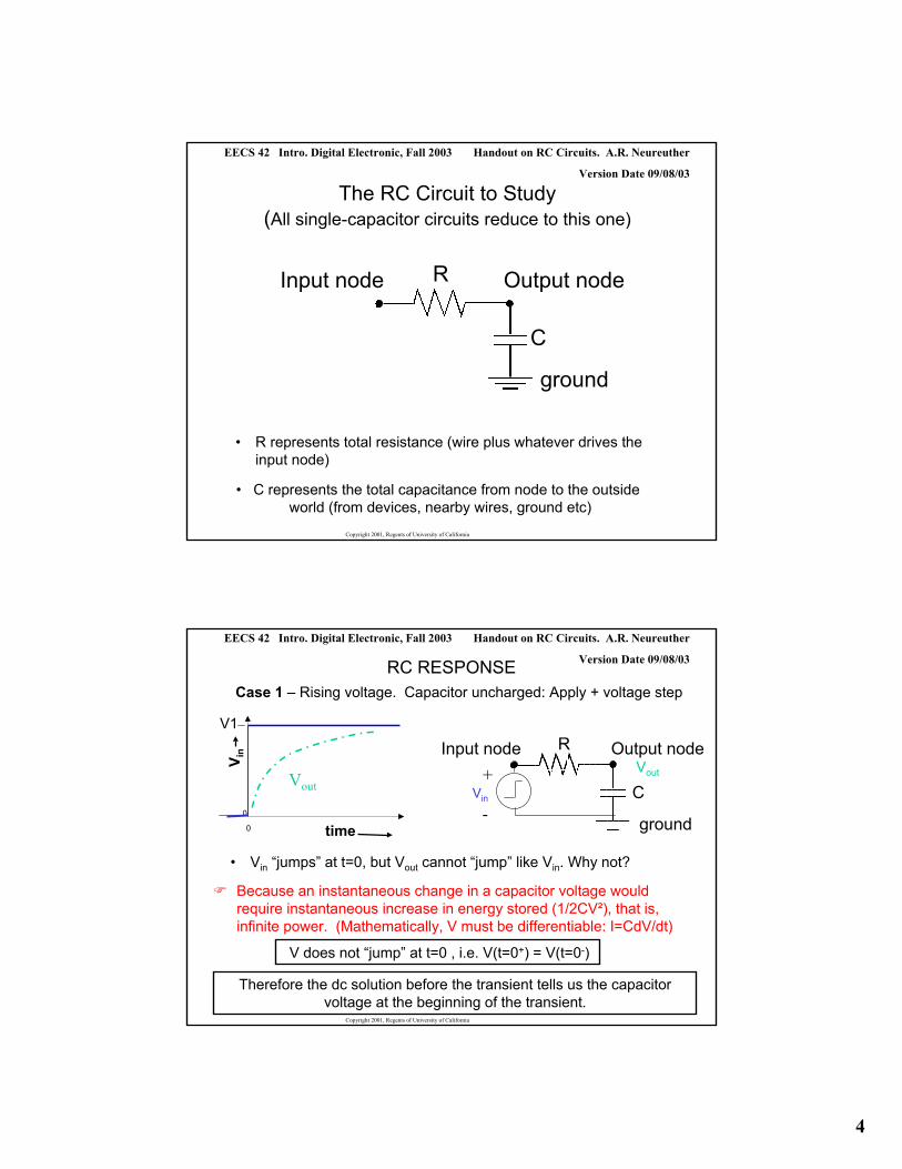
4
Copyright 2001, Regents of University of California
Handout on RC Circuits. A.R. Neureuther
Version Date 09/08/03
EECS 42 Intro. Digital Electronic, Fall 2003
The RC Circuit to Study(All single-capacitor circuits reduce to this one)
• R represents total resistance (wire plus whatever drives the input node)
Input node Output node
ground
R
C
• C represents the total capacitance from node to the outside world (from devices, nearby wires, ground etc)
Copyright 2001, Regents of University of California
Handout on RC Circuits. A.R. Neureuther
Version Date 09/08/03
EECS 42 Intro. Digital Electronic, Fall 2003
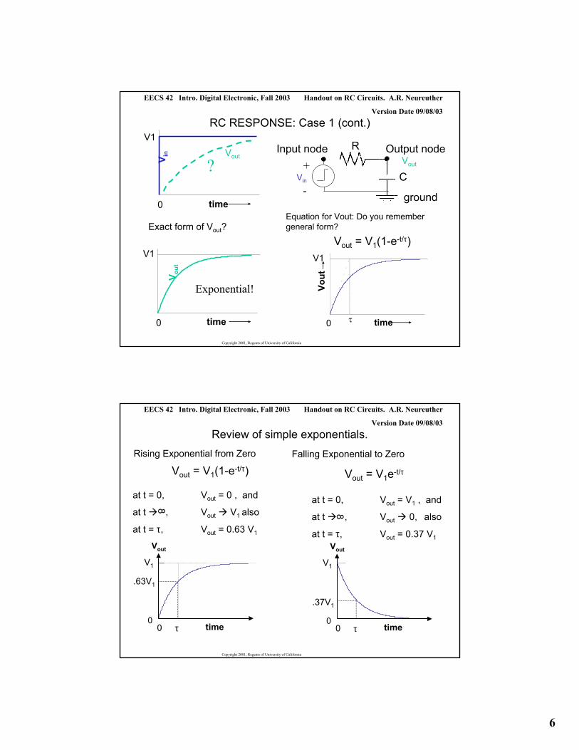
RC RESPONSE
• Vin “jumps” at t=0, but Vout cannot “jump” like Vin. Why not?
Case 1 – Rising voltage. Capacitor uncharged: Apply + voltage step
Because an instantaneous change in a capacitor voltage would require instantaneous increase in energy stored (1/2CV²), that is, infinite power. (Mathematically, V must be differentiable: I=CdV/dt)
Input node Output node
ground
R
CVin
Vout+
-
V does not “jump” at t=0 , i.e. V(t=0+) = V(t=0-)
time
V in
0
0
V1
Vout
Therefore the dc solution before the transient tells us the capacitor voltage at the beginning of the transient.

5
Copyright 2001, Regents of University of California
Handout on RC Circuits. A.R. Neureuther
Version Date 09/08/03
EECS 42 Intro. Digital Electronic, Fall 2003
RC RESPONSECase 1 Continued – Capacitor uncharged: Apply voltage step
After the transient is over (nothing changing anymore) it means d(V)/dt = 0 ; that is all currents must be zero. From Ohm’s law, the voltage across R must be zero, i.e. Vin = Vout.
• Vout approaches its final value asymptotically (It never actually gets exactly to V1, but it gets arbitrarily close). Why?
That is, Vout → V1 as t → ∞. (Asymptotic behavior)
time
V in
0
0
V1
Vout
Input node Output node
ground
R
CVin
Vout+
-
Again the dc solution (after the transient) tells us (the asymptotic limit of) the capacitor voltage during the transient.
Copyright 2001, Regents of University of California
Handout on RC Circuits. A.R. Neureuther
Version Date 09/08/03
EECS 42 Intro. Digital Electronic, Fall 2003
RC RESPONSEExample – Capacitor uncharged: Apply voltage step of 5 V
• We know this because of the pre-transient dc solution (V=0) and post-transient dc solution (V=5V).
• Clearly Vout starts out at 0V ( at t = 0+) and approaches 5V.
time
V in
0
0
5
Vout
Input node Output node
ground
R
CVin
Vout+
-
So we know a lot about Vout during the transient - namely its initial value, its final value , and we know the general shape .
We even know the initial slope from I = C(dV/dt) as
(dV/dt) = (1/C)I = (1/C)(Vin –0)/R =(Vin –0)/(RC)
6
Copyright 2001, Regents of University of California
Handout on RC Circuits. A.R. Neureuther
Version Date 09/08/03
EECS 42 Intro. Digital Electronic, Fall 2003
RC RESPONSE: Case 1 (cont.)
timeVo
ut00
V1
τ
Exact form of Vout?Equation for Vout: Do you remember general form?
time
V out
0
V1
Exponential!
time
V in
0
V1
?Vout
Input node Output node
ground
R
CVin
Vout+
-
Vout = V1(1-e-t/τ)
Copyright 2001, Regents of University of California
Handout on RC Circuits. A.R. Neureuther
Version Date 09/08/03
EECS 42 Intro. Digital Electronic, Fall 2003
Review of simple exponentials.Rising Exponential from Zero Falling Exponential to Zero
at t = 0, Vout = 0 , and
at t , Vout V1 also
at t = τ, Vout = 0.63 V1
8 at t = 0, Vout = V1 , and
at t , Vout 0, also
at t = τ, Vout = 0.37 V1
8
time
Vout
00
V1
τ
.63V1
Vout
V1
time00
τ
.37V1
Vout = V1(1-e-t/τ) Vout = V1e-t/τ

7
Copyright 2001, Regents of University of California
Handout on RC Circuits. A.R. Neureuther
Version Date 09/08/03
EECS 42 Intro. Digital Electronic, Fall 2003
Further Review of simple exponentials.Rising Exponential from Zero Falling Exponential to Zero
We can add a constant (positive or negative)
.63V1+ V2
Vout
0
V1 + V2
time0 τ
V2
time
Vout
00
V1 + V2
τ
.37V1 + V2
V2
Vout = V1(1-e-t/τ) Vout = V1e-t/τ
Vout = V1(1-e-t/τ) + V2 Vout = V1e-t/τ + V2
Copyright 2001, Regents of University of California
Handout on RC Circuits. A.R. Neureuther
Version Date 09/08/03
EECS 42 Intro. Digital Electronic, Fall 2003
Further Review of simple exponentials.Rising Exponential Falling Exponential
Both equations can be written in one simple form:
Thus: if B < 0, rising exponential; if B > 0, falling exponential
Initial value (t=0) : Vout = A + B. Final value (t>>τ): Vout = A
time
Vout
00
A+B
A
Here B > 0
Vout
0
A
time0
A+B
Here B < 0
Vout = V1(1-e-t/τ) + V2Vout = V1e-t/τ + V2
Vout = A + Be-t/τ

8
Copyright 2001, Regents of University of California
Handout on RC Circuits. A.R. Neureuther
Version Date 09/08/03
EECS 42 Intro. Digital Electronic, Fall 2003
RC RESPONSE: Case 1 (Rising exponential)
• How is τ related to R and C ?
time
Vin
00
V1
time
Vout
0
V1
τ
– If C is bigger, it takes longer (τ↑ ).– If R is bigger, it takes longer (τ↑ ).
Thus, τ is proportional to RC.
In fact, τ = RC !
Vin
RVout
C
iCiR
Vout = V1(1-e-t/τ)
Thus, Vout = V1(1-e-t/RC)
Copyright 2001, Regents of University of California
Handout on RC Circuits. A.R. Neureuther
Version Date 09/08/03
EECS 42 Intro. Digital Electronic, Fall 2003
RC RESPONSE: Case 1 (cont.))e1(VV that Proof RC/t
1out−−=
Vin
RVout
C
iCiR
law) ce(capacitan i
law) s(Ohm'
C dtdVC
RVVi
out
outinR
=
−=
! iiBut CR =
)VV(RC1
dtdV
dt
dVCR
VV Thus,
outinout
outoutin
−=
=−
or

9
Copyright 2001, Regents of University of California
Handout on RC Circuits. A.R. Neureuther
Version Date 09/08/03
EECS 42 Intro. Digital Electronic, Fall 2003
RC RESPONSE Case 1 (cont.))RC/te1(1VoutV that Proof −−=
+==
==
0tat 0outV and
constant1VinVBut
I claim that the solution to this first-order linear differential equation is:
)RC/te1(1VoutV −−=
We have: )outVin(VRC1
dtoutdV
−= Proof by substitution:
and
OK 0tat 0Vout+==
))/1(11(1/RC
1V--
)(1
RCteVVRCRCte
outVinVRCdtoutdV
−−−=−
↓
−=
// / /
?
?
RCteRCVRCte /1/
RC1V −=−
clearly
Copyright 2001, Regents of University of California
Handout on RC Circuits. A.R. Neureuther
Version Date 09/08/03
EECS 42 Intro. Digital Electronic, Fall 2003
RC RESPONSE (cont.)
Generalization
Vin switches at t = 0; then for any time interval t > 0, in which Vin is a constant, Vout is always of the form:
We determine A and B from the initial voltage on C, and the value of Vin. Assume Vin “switches” at t=0 from Vco to V1:
voltageinitial VV 0tat First, CoC ≡=
Thus, CoVBA =+
1C VV ,t as →∞→
Thus, 1Co VVB −=⇒1VA =
Vin
RVout
C
iCiR
Vout = A + Be-t/RC
RC is RTHC where RTH is the Thevenin Resistance seen C with independent sources set to zero.
10
Copyright 2001, Regents of University of California
Handout on RC Circuits. A.R. Neureuther
Version Date 09/08/03
EECS 42 Intro. Digital Electronic, Fall 2003
Re-Cap: Charging and discharging in RC Circuits
Last Time:Input node Output node
ground
R
CVin
Vout+
-
We learned that simple the simple RC circuit with a step input has a universal exponential solution of the form:
Example 0: R = 1K, C = 1pF, Vin steps from zero to 10V at t=0:
time
Vin
0
0
10
Vout
1nsec
6.3V
1) Initial value of Vout is 0
2) Final value of Vout is 10V
3) Time constant is RC = 10-9 sec
4) Vout reaches 0.63 X 10 in 10-9 sec
Vout = A + Be-t/RC
Copyright 2001, Regents of University of California
Handout on RC Circuits. A.R. Neureuther
Version Date 09/08/03
EECS 42 Intro. Digital Electronic, Fall 2003
Charging and discharging in RC Circuits - Example 1 (rising exponential) continued -
Input node Output node
ground
R
CVin
Vout+
-
time
Vin
0
0
10
Vout
1nsec
6.3V
We simply used the dc solution for t<0 and the dc solution for t>>0 to get the limits and we used the time constant to get the horizontal scale. We only need the equation to remind us the solution is an exponential. So this will be the basis of our easy method.
For this example: R = 1K, C = 1pF,Vin steps from zero to 10V at t=0:
Note that we found this graph without even using the equation (That is we did not try to evaluate A and B).Vout = A + Be-t/RC
Vout starts at 0, ends at 10 and has time constant of 1nsec
Vout = 10 - 10e-t/1nsec
11
Copyright 2001, Regents of University of California
Handout on RC Circuits. A.R. Neureuther
Version Date 09/08/03
EECS 42 Intro. Digital Electronic, Fall 2003
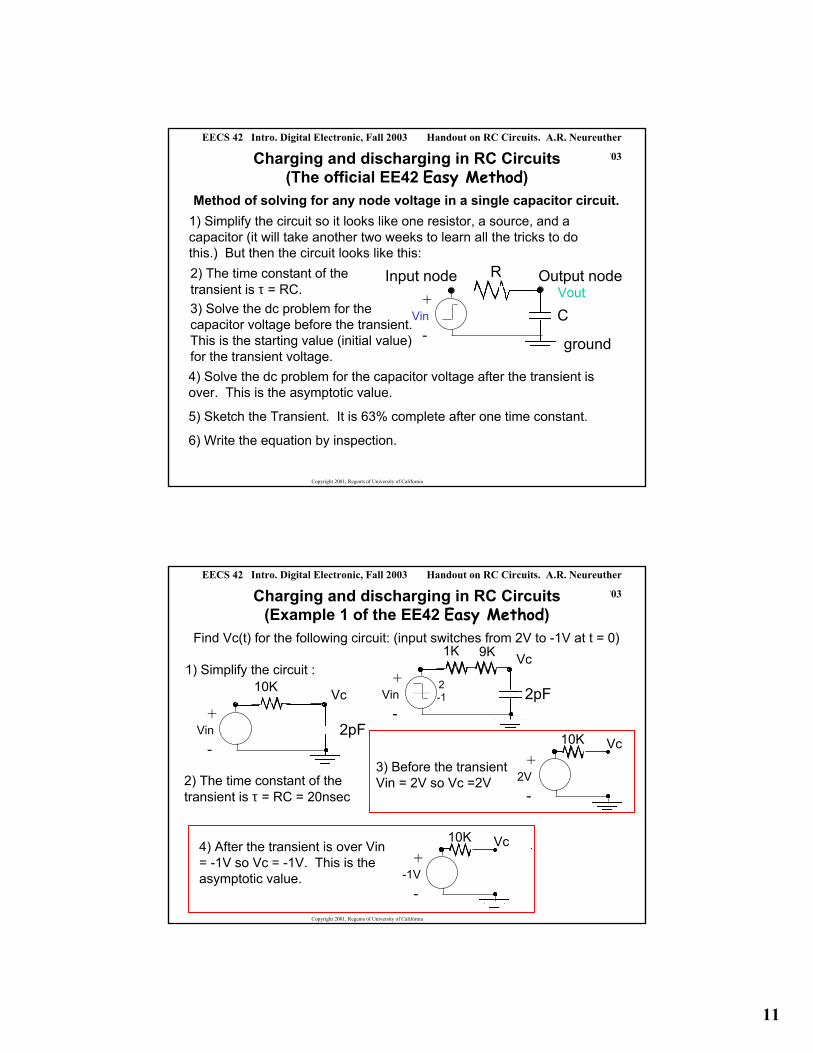
Charging and discharging in RC Circuits(The official EE42 Easy Method)
Input node Output node
ground
R
CVin
Vout+
-
4) Solve the dc problem for the capacitor voltage after the transient is over. This is the asymptotic value.
5) Sketch the Transient. It is 63% complete after one time constant.
6) Write the equation by inspection.
1) Simplify the circuit so it looks like one resistor, a source, and a capacitor (it will take another two weeks to learn all the tricks to do this.) But then the circuit looks like this:
Method of solving for any node voltage in a single capacitor circuit.
2) The time constant of the transient is τ = RC.3) Solve the dc problem for the capacitor voltage before the transient. This is the starting value (initial value) for the transient voltage.
Copyright 2001, Regents of University of California
Handout on RC Circuits. A.R. Neureuther
Version Date 09/08/03
EECS 42 Intro. Digital Electronic, Fall 2003
Charging and discharging in RC Circuits(Example 1 of the EE42 Easy Method)
1) Simplify the circuit :
Find Vc(t) for the following circuit: (input switches from 2V to -1V at t = 0)
2) The time constant of the transient is τ = RC = 20nsec
1K
2pFVin
Vc+
-
2 -1
9K
10K
2pFVin
Vc+
-3) Before the transient Vin = 2V so Vc =2V
10K
2V
Vc+
-
4) After the transient is over Vin = -1V so Vc = -1V. This is the asymptotic value.
10K
-1V
Vc+
-
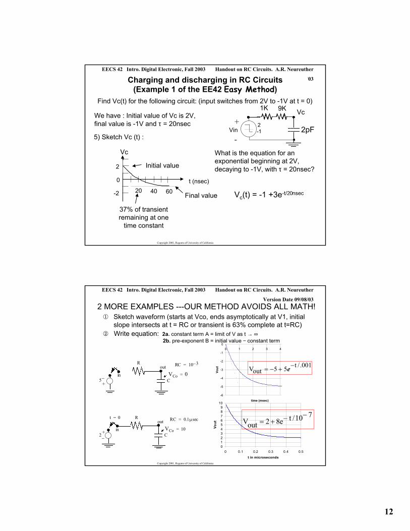
12
Copyright 2001, Regents of University of California
Handout on RC Circuits. A.R. Neureuther
Version Date 09/08/03
EECS 42 Intro. Digital Electronic, Fall 2003
Charging and discharging in RC Circuits(Example 1 of the EE42 Easy Method)
We have : Initial value of Vc is 2V, final value is -1V and τ = 20nsec
Find Vc(t) for the following circuit: (input switches from 2V to -1V at t = 0)1K
2pFVin
Vc+
-
2 -1
9K
5) Sketch Vc (t) :
t (nsec)
2
-2
0
Vc
20 40 60
37% of transient remaining at one
time constant
Final value
Initial value
What is the equation for an exponential beginning at 2V, decaying to -1V, with τ = 20nsec?
Vc(t) = -1 +3e-t/20nsec
Copyright 2001, Regents of University of California
Handout on RC Circuits. A.R. Neureuther
Version Date 09/08/03
EECS 42 Intro. Digital Electronic, Fall 2003
2 MORE EXAMPLES ---OUR METHOD AVOIDS ALL MATH!Sketch waveform (starts at Vco, ends asymptotically at V1, initial slope intersects at t = RC or transient is 63% complete at t=RC)Write equation: 2a. constant term A = limit of V as t → ∞
2b. pre-exponent B = initial value − constant term
in
Rout
VCo 0=
+−5
RC 10 3–=
C
in
Rout
VCo 10=
+−
2
RC 0.1µsec=
C
t 0=
-6
-5
-4
-3
-2
-1
00 1 2 3 4
time (msec)
Vout 001./t55outV −+−= e
710/te82outV−−+=
0123456789
10
0 0.1 0.2 0.3 0.4 0.5t in microseconds
Vout

13
Copyright 2001, Regents of University of California
Handout on RC Circuits. A.R. Neureuther
Version Date 09/08/03
EECS 42 Intro. Digital Electronic, Fall 20034 Examples
inR
out
C
+
−V1
t 0=
sec 01.0RC =
V 5CoV =
0
2
4
6
8
10
12
0 0.01 0.02 0.03 0.04 0.05
time (sec)
Vou
t A= 10B= -10
0
2
4
6
8
10
12
0 0.01 0.02 0.03 0.04 0
time (sec)
Vout
A= 10B= -5
0
2
4
6
8
10
12
0 0.01 0.02 0.03 0.04 0
time (sec)
Vout
A=0B=0
0
2
4
6
8
10
12
0 0.01 0.02 0.03 0.04 0.05time (sec)
Vout
A=0B=501V =
101V =
0CoV =
RC/tout BeAV −+=
Copyright 2001, Regents of University of California
Handout on RC Circuits. A.R. Neureuther
Version Date 09/08/03
EECS 42 Intro. Digital Electronic, Fall 2003
0
1
2
3
4
5
6
0 2 4 6 8 10
time (microseconds)
Vout
in
Rout
VCo 5V=
RC 2µ sec=
C
t 1µsec=
COMPLICATION: Event Happens at t ≠ 0(Solution: Shift reference time to time of event)
Example: switch closes at 1µsec
6102
)610(
5−×
−−−
=
t
eV
We shift the time axis here by one microsecond, i.e.imagine a new time coordinate t* = t-1µsec so thatin the new time domain, the event happens at t* = 0 and our standard solution applies. Of course we replace t* by t -1µsec in the equations and plots. Thusinstead of t* =0 we have t = 1µsec, etc.
14
Copyright 2001, Regents of University of California
Handout on RC Circuits. A.R. Neureuther
Version Date 09/08/03
EECS 42 Intro. Digital Electronic, Fall 2003
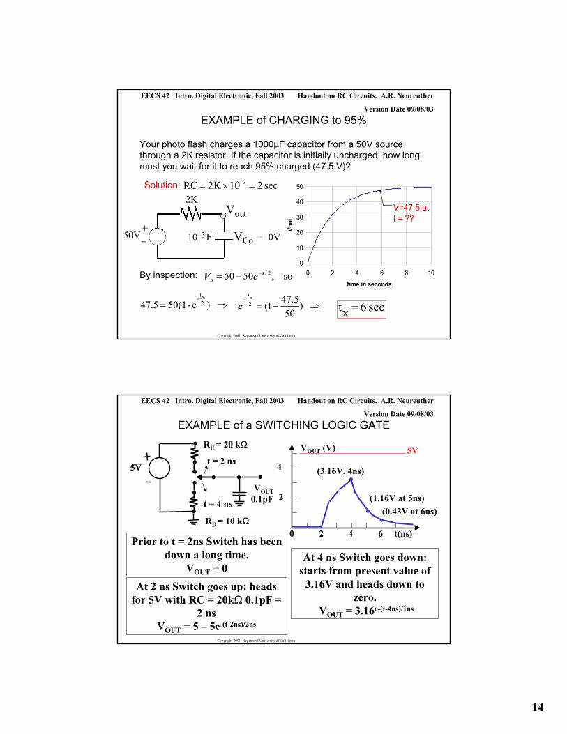
EXAMPLE of CHARGING to 95%
Your photo flash charges a 1000µF capacitor from a 50V source through a 2K resistor. If the capacitor is initially uncharged, how long must you wait for it to reach 95% charged (47.5 V)?
sec 6xt =
0
10
20
30
40
50
0 2 4 6 8 10
time in secondsVo
ut
V=47.5 at t = ??
Vout
VCo 0V=+−
50V 10 3– F
2K
By inspection: so ,5050 2/to eV −−=
)e-50(147.5 2t- x
⇒= )50
5.471( 2 ⇒−=− xt
e
Solution: sec 210K2RC 3 =×= −
Copyright 2001, Regents of University of California
Handout on RC Circuits. A.R. Neureuther
Version Date 09/08/03
EECS 42 Intro. Digital Electronic, Fall 2003
EXAMPLE of a SWITCHING LOGIC GATERU = 20 kΩ
VOUT
5V
RD = 10 kΩ
t = 2 ns
t = 4 ns
0 2 4 6 t(ns)
VOUT (V)
2
4 (3.16V, 4ns)
(1.16V at 5ns)(0.43V at 6ns)
At 4 ns Switch goes down: starts from present value of
3.16V and heads down to zero.
VOUT = 3.16e-(t-4ns)/1ns
At 2 ns Switch goes up: heads for 5V with RC = 20kΩ 0.1pF =
2 nsVOUT = 5 – 5e-(t-2ns)/2ns
Prior to t = 2ns Switch has been down a long time.
VOUT = 0
0.1pF
5V