charge-sensitive front-end electronics with operational ... front-end electronics with operational...
TRANSCRIPT

Preprint typeset in JINST style - HYPER VERSION
Charge-sensitive front-end electronics withoperational amplifiers for CdZnTe detectors
P. Födischa∗, M. Berthelb, B. Langea, T. Kirschkea, W. Enghardtb,c,d and P. Kaevera
aHelmholtz-Zentrum Dresden - Rossendorf, Department of Research Technology,Bautzner Landstr. 400, 01328 Dresden, Germany
bOncoRay - National Center for Radiation Research in Oncology, Faculty of Medicine andUniversity Hospital Carl Gustav Carus, Technische Universität Dresden,Fetscherstr. 74, PF 41, 01307 Dresden, Germany
cHelmholtz-Zentrum Dresden - Rossendorf, Institute of RadiooncologyBautzner Landstr. 400, 01328 Dresden, Germany
dGerman Cancer Consortium (DKTK) and German Cancer Research Center (DKFZ)Im Neuenheimer Feld 280, 69120 Heidelberg, Germany
E-mail: [email protected]
ABSTRACT: Cadmium zinc telluride (CdZnTe, CZT) radiation detectors are suitable for a varietyof applications, due to their high spatial resolution and spectroscopic energy performance at roomtemperature. However, state-of-the-art detector systems require high-performance readout elec-tronics. Though an application-specific integrated circuit (ASIC) is an adequate solution for thereadout, requirements of high dynamic range and high throughput are not available in any com-mercial circuit. Consequently, the present study develops the analog front-end electronics with op-erational amplifiers for an 8× 8 pixelated CZT detector. For this purpose, we modeled an electricalequivalent circuit of the CZT detector with the associated charge-sensitive amplifier (CSA). Basedon a detailed network analysis, the circuit design is completed by numerical values for various fea-tures such as ballistic deficit, charge-to-voltage gain, rise time, and noise level. A verification ofthe performance is carried out by synthetic detector signals and a pixel detector. The experimentalresults with the pixel detector assembly and a 22Na radioactive source emphasize the depth depen-dence of the measured energy. After pulse processing with depth correction based on the fit of theweighting potential, the energy resolution is 2.2% (FWHM) for the 511keV photopeak.
KEYWORDS: Analogue electronic circuits, Front-end electronics for detector readout, Gammadetectors.
∗Corresponding author.
arX
iv:1
603.
0509
8v4
[ph
ysic
s.in
s-de
t] 1
9 A
ug 2
016

Contents
1. Introduction 1
2. Basic design considerations 22.1 CZT detector assembly 22.2 Electrical characteristics of a CZT pixel detector 32.3 High voltage biasing and grounding 42.4 Signal formation in CZT detectors 62.5 Readout concepts 82.6 Operational amplifier 11
3. Circuit design of a charge-sensitive preamplifier 133.1 Circuit analysis 143.2 Charge-to-voltage transfer function 173.3 Input coupling of the CSA 193.4 Noise 20
4. Implementation 23
5. Results 245.1 Test pulse input 255.2 Pixel detector 26
6. Summary 30
1. Introduction
Cadmium zinc telluride (CdZnTe, CZT) is a room-temperature semiconductor material for radi-ation detectors [1]. It is available in compact detector units with highly segmented pixel layoutsand is ideally suited for high-resolution gamma-ray spectroscopy [2] and 3D imaging [3]. As hasbeen previously reported, CZT detectors have been used in Compton camera systems [4, 5, 6].With regard to our investigations, CZT detectors are potentially useful in imaging systems for pro-ton therapy [7, 8, 9, 10]. State-of-the-art readout systems for highly segmented CZT detectors areconventionally built with an application-specific integrated circuit (ASIC) [11, 12]. The ASICsare optimized for gamma-ray spectroscopy. Low energy range, usually up to 2MeV [7, 12, 13],limited count rate capability, and poor availability and product life cycle are unsolved challengesof an ASIC-based readout system for an imaging system in proton therapy. In this environment,high energies up to 7MeV and count rates up to 1Mcps have to be handled [14, 15, 16]. Instead
– 1 –

of using an ASIC for the readout electronics, commercial off-the-shelf (COTS) operational am-plifiers have been used for the front-end electronics [17]. Along with space-saving multi-channelanalog-to-digital converters (ADC) and a field-programmable gate array (FPGA), all tasks relatedto the signal acquisition and processing can be done with a COTS system. A programmable digitalsystem benefits from its versatility, which is needed for the evaluation of a detector system for newapplications like proton therapy. Even for applications in a fixed installation, a system made ofCOTS components provides the advantages of proven reliability and life-cycle support.
In general the front-end electronics are the key element of the overall performance of thedetector system. Our goal is to maximize the dynamic range of the front-end electronics since theCZT is exposed to high-energy gamma rays, but also has to detect low-energy scatter events usedfor the Compton imaging. As this is the main goal, which cannot be solved with a state-of-the-artASIC, the timing information of an interaction must be preserved by the readout system. MostASICs merely include simple analog signal processing (e.g. leading-edge trigger for timing andpeak-hold circuit for energy information), making pulse shape analysis or advanced timing difficultor even impossible. As the design of the front-end electronics is a tradeoff between bandwidth,noise, complexity, size, and costs, the best solution must be driven by the application. For theprototype of a Compton camera, we investigate a space-saving and simple circuit design withminimal components. The system must include at least 65 analog readout channels, set up withCOTS voltage feedback operational amplifiers.
2. Basic design considerations
2.1 CZT detector assembly
For a medical imaging application, we use a CZT detector as the scattering layer in a Comptoncamera. In our case, this is a pixelated CZT radiation detector from Redlen Technologies [18].The detector size is 19.42 × 19.42mm2 with a thickness of 5mm. Towards the continuous planarelectrode on the back side, there are 64 pixel electrodes aligned in an 8 × 8 array on the front side.The size of a pixel pad is 2.2×2.2mm2 for all pixels except the corner pixels with 1.98× 1.98mm2.In addition, a steering grid surrounds all pixels. The inter-pixel space is 0.26mm. The bulk deviceand an assembled detector are shown in figure 1. The detector is mounted on a printed circuitboard (PCB) with the continuous planar electrode on top. A bond wire is attached to a copper padon the carrier PCB. Furthermore, a conductive adhesive on each pixel pad ensures the electricalconnection to the pixel array on the PCB. An underfill between the pixel array and the PCB supportsthe adhesive connection and improves the mechanical stability. We also decided to use a 3.2mm-thick FR-4 material for the PCB to enhance the robustness of the assembly. The electrodes ofthe detector are accessible via rugged high-speed connectors on the bottom side. To shield thedetector against visible light, a 3D-printed cap is attached above the detector on the top of thecarrier board. Our front-end electronics are designed to work with this type of detector assembly,and the readout boards are plugged into the side faces of the detector assembly (see figure 22)so a stacked system with arbitrary depth, as required for the evaluation of the Compton camera,can be easily constructed. Further investigations on ruggedization of CZT detectors and detectorassemblies have been presented in [19].
– 2 –

Figure 1. A 5mm thick pixelated CZT detector from Redlen Technologies [18] with 8 × 8 electrodes (each2.2mm × 2.2mm) on the front side (left) and a continuous planar electrode (19.42mm × 19.42mm) on theback side (right). The detector is mounted on a 3.2mm-thick carrier board with rugged connectors on thebottom side.
2.2 Electrical characteristics of a CZT pixel detector
From the electrical point of view, a CZT detector can be modeled with the equivalent circuit shownin figure 2. With an external operating voltage at the electrodes of the detector, the terminals arereferred to as cathode and anode in accordance with the applied polarity. Usually, the continuouselectrode is biased with a negative potential and the pixel electrodes are at ground potential. For anideal detector material, this would force the negative charge carriers (electrons) to move towardsthe anode and the positive charge carriers (holes) to move towards the cathode. As a consequenceof charge trapping due to structural defects, impurities, and irregularities of the material [20], themobility and lifetime of the holes in CZT are very poor compared to the electrons [21]. Onlythe moving electrons induce a signal on the electrodes, while the portion of the signal due to theholes may be neglected. Thus, if the generated electrons move to the position-sensitive side ofthe detector, the overall detection performance is improved. As the readout electronics are directlyconnected to the electrodes, the electrical characteristics of the detector influence the dynamic be-havior of the entire circuit. Finally, the network model for the readout electronics must include theelectrical equivalent circuit of the detector. In general, a very simple equivalent circuit is adequateto model the properties of the detector. As summarized in figure 2, it is a passive two-terminal com-ponent with a permittivity and a resistance. A capacitor represents the permittivity of the materialand the conductance is modeled as a resistor. For the evaluated pixelated CZT detector, the capac-itance can be roughly approximated by the model of the parallel-plate capacitor with an electrodearea A separated by the distance d. That capacitance C is calculated by
C = ε0εrAd, (2.1)
where ε0 is the vacuum permittivity and εr is the relative permittivity of CZT. For the detector inthis study, the values are A = 377mm2, d = 5mm. In practical terms, the bias voltage does not
– 3 –

influence the relative permittivity in the applicable voltage range up to−600V. The capacitance ofthe detector is therefore largely independent of the bias voltage [22]. The value of εr depends on themanufacturing process, but ranges from 10 to 11 [21, 23]. Thus, the entire bulk capacitance is inthe range from 6.6pF to 7.4pF. The capacitance of a single pixel can also be calculated by eq. 2.1,where the size of the pixel determines the value of A [24]. With the same assumption for εr, thepixel capacitance is in the range from 69fF to 95fF, including the smaller corner pixels. Besidesthe estimation of capacitance, the bulk resistivity of the detector is needed to model the electricalcharacteristics. We measured the leakage current of the assembled CZT detector from figure 1 witha precision high-voltage source with current monitor (Iseg SHQ series) [25]. This device reportsa current of 10nA±1nA with a detector bias voltage of −500V. For a homogenous material, theresistance is defined as:
R = ρdA
(2.2)
where ρ is the resistivity of the material. Our measurement corresponds to a resistor of 50GΩ forthe two-terminal equivalent circuit or a resistivity of 4 · 1011Ωcm. This is in accordance with thevalues from the datasheet (ρ > 1011Ωcm) from Redlen [18].
RD CD
Anode
Cathode
Figure 2. An electrical equivalent circuit of a CZT detector. The bulk resistivity is modeled with the resistorRD, which is typically of several tens of GΩ. The capacitor CD represents the parallel-plate geometry of theelectrodes. Its value can be estimated with eq. 2.1.
Finally, the electrical characteristics of a CZT crystal mainly depend on the manufacturingprocess. If they cannot be experimentally verified, the values for the components of the electricalequivalent circuit can be estimated with the geometry of the detector and the constants from theliterature by eqn. 2.1 and 2.2. The equivalent circuit shown in figure 2 is the simplest electricalrepresentation of the detector unit. It does not model a frequency dependency with a complexpermittivity. Additionally, the stray capacitances introduced by the traces and the carrier boarditself, cross-coupling between pixels, and any inductivities of the connectors are ignored. However,a well-designed PCB layout can minimize these effects.
2.3 High voltage biasing and grounding
A fundamental operating condition for a CZT detector is the presence of an electric field betweenthe electrodes. Thus, the charge carriers generated by incident radiation move towards the elec-trodes. Typical electric field strengths for CZT detectors are in the range of 1 kV
cm [18]. As thecontinuous electrode of the detector is biased with a negative voltage, the ground potential is con-nected to the pixelated electrodes on the opposite side. In general, the high voltage with low ripple
– 4 –

is generated by an external power supply connected to the detector via a cable or PCB traces. To re-duce any pickup noise related to electromagnetic interference, we put a high-voltage filter close tothe detector electrode. This is in the simplest case a passive first-order low-pass filter (RC networkshown in figure 3). The value of the resistor RB should be chosen to minimize the voltage drop
+−
V
R
C
RB
iD RD CD
Anodes
Cathode
High voltage bias CZT Detector Readout
Ground
Figure 3. Basic connection scheme of the CZT detector. A high voltage supply with an RC low-pass filterand a resistor RB are used to generate the bias voltage for the cathode. The readout electronics are directlyconnected to the cathode and anodes of the detector. The anodes are biased by ground signal of the readoutelectronics, and consequently both ground potentials must be tied together.
across the high-voltage filter and maximize the voltage across the detector. The value of the filtercapacitor C should be as high as possible to achieve the best noise filtering. According to eqs. 2.1and 2.2, the capacitance is inversely proportional to the resistance. Therefore, the capacitor C mustbe chosen, such that the insulation resistance of the dielectric material is much higher than theresistance of the detector. Commercial capacitors of class 1 have an insulation resistance of morethan 100GΩ with a maximum capacitance of 10nF. Thus, a passive first-order low-pass filter witha cutoff frequency below 1Hz is possible (e.g. R = 47MΩ, C = 10nF). As a noise-filtered voltageis the output of the RC circuit, it cannot be directly connected to the electrode in order to bias thedetector. One reason for this is that the filter capacitor C would be in parallel with the capacitanceCD of the detector. A bias resistor RB of 47MΩ separates the filter network from the detector.Another point that has to be taken into account is the path of current flow generated by the detector.The current should not flow into the high-voltage source. This can be ensured by choosing a highresistance for biasing the detector, so that the time constant RBC is much larger than the time con-stant of the readout electronics [26]. The active components of the readout electronics have theirown power supply, which is separated from the high-voltage supply. Further, the anodes are biasedwith the ground potential of the readout electronics (signal ground in figure 3). Both grounds haveto be at the same potential and must be tied together. The electric field between the cathode andthe anodes is therefore referenced to a known potential.
– 5 –

2.4 Signal formation in CZT detectors
As implied, incident radiation hitting the detector generates free charge carriers. These electronsand holes move towards the electrodes because of the applied electric field. However, the generatedcharge is proportional to the incident gamma-ray energy and the signal of the detector is an electriccurrent. The induced current through an electrode is defined as
i = q→v→E0 (x) , (2.3)
where q is the moving charge,→v is the instantaneous velocity of the charge q and
→E0 (x) is the
weighting field associated with the electrode at the position x of the charge [27]. The weightingpotential ϕ0(x) is defined as
→E0 (x) =−∇
→ϕ0 (x) , (2.4)
by setting one electrode to unit potential and all others to zero. For a parallel-plate geometry ofa detector, where the widths in x and y dimensions of the electrodes are much larger than thethickness z, the electric field inside the detector is distributed homogeneously with a constant field
strength. Therefore, the weighting field→E0 (x) is equal to the electric field, and, solving eq. 2.4 in
the z-dimension, the normalized weighting potential ϕ0C(z) of the cathode is a linear function [27]:
ϕ0C(z) = z,0≤ z≤ 1 . (2.5)
The solution for the Poisson equation in two dimensions was given by [24, 28]. These authorspresented an equation for the calculation of the weighting potential for a detector with a segmentedelectrode layout. By setting one dimension of the pixel area to zero and normalizing the thicknessz of the detector to 1, the weighting potential ϕ0A of a single pixel with the normalized width a canbe calculated as
ϕ0A(x,z) =1π
arctan(
sin(πz)sinh(π a2)
cosh(πx)− cos(πz)cosh(π a2)
), (2.6)
where x and z are the coordinates and 0 ≤ z ≤ 1. The weighting potentials are shown in figure 4.The weighting field E0(z) under the collecting electrode (x = 0, y = 0) can be calculated by solvingeq. 2.4 with eq. 2.6. This results in the following equation:
E0(z) =sinh(π a
2)
cos(πz)− cosh(π a2)
. (2.7)
As we can estimate the weighting field of the detector with eq. 2.7, the next step is to calculatethe expected electric current to simulate the transient behavior of the detector signals. With theassumption that the electric field E is constant and homogenous across the detector because allanodes are at the same potential, the electric field is calculated by
E =Vd, (2.8)
where V is the applied bias voltage and d is the thickness of the detector. Then, the velocity v of amoving charge q in the detector is calculated by
v = µeE , (2.9)
– 6 –

0 1 2 3 4 5z / mm
0
0.2
0.4
0.6
0.8
1
Wei
ghtin
g po
tent
ial ?
0
0 1 2 3 4 5z / mm
0
0.2
0.4
0.6
0.8
1
Wei
ghtin
g po
tent
ial ?
0
Figure 4. The weighting potentials of the cathode (bottom) and pixel anode (top) of the 5mm-thick detector.The cathode is located at position z= 0mm. The right plots show the weighting potential under the collectingelectrode (x = y = 0mm).
where µ is the mobility of the charge carriers (electrons). A typical value of µe for a CZT is about1000 cm2
Vs [29, 30]. With the ionization energy Ei = 4.64eV for CZT [21] and the incident radiationEγ , the generated moving charge q is defined as
q = eEγ
Ei(2.10)
where e is the elementary charge. By inserting the eqs. 2.7, 2.8, 2.9, 2.10 into eq. 2.3, the detectorcurrent can be numerically estimated. An example of incident radiation of Eγ = 511keV is shownin figure 5.
0 200 400 600Time / ns
0
20
40
60
80
100
120
140
Cat
hode
cur
rent
/ nA E=800 V/cm
E=1000 V/cmE=1200 V/cm
0 200 400 600Time / ns
0
20
40
60
80
100
120
140
Ano
de c
urre
nt /
nA
E=800 V/cmE=1000 V/cmE=1200 V/cm
Figure 5. Induced current i on the detector electrodes for incident radiation with an energy of 511keV. Theleft plot shows the current induced on the cathode and the right plot shows the current induced on an anodepixel. The signals are calculated with eq. 2.3. An increased electric field strength E causes a higher currenti with shorter drift times tD. The generated charge remains constant.
Figure 5 shows the currents flowing through the electrodes for an interaction at the cathodeside of the detector. If the depth of interaction is closer to the anode side, the total charge collection
– 7 –

is incomplete, as the fraction of charge from the holes cannot be measured. This circumstanceintroduces a depth dependence and requires a correction for spectroscopic applications.
2.5 Readout concepts
The results from figure 5 give an estimate of the required sensitivity for the readout electronics. Thesignals are in the range of several nA (e.g. 8nA for 100keV at the cathode with an electric field of1200 V
cm ). In addition, the drift time tD can be as short as 40ns if the interaction takes place in thelast 10% of the detector volume at the anode side. As the detector signals are electric currents, thesimplest way to acquire these signals is to use a shunt resistor and a measurement of the voltagedrop across this resistor. Finally, the measured transient voltage signal could be fed to an arbitrarysignal processing system. In fact, a single resistor would be the simplest, smallest, and cheapestsolution for the front-end electronics. With a resistor in the range of some MΩ, i.e. is small enoughto force the detector current to flow into it, a voltage drop in the range of some mV is generated.This is sufficient for most signal processing systems. However, this concept suffers from a lackof bandwidth. As the left circuit in figure 6 shows, the induced current will flow through RS, butthe RC time constant of this two-terminal circuit determines the bandwidth and therefore the risetime of this circuit. Moreover, the detector adds its own capacitance to the shunting elements. The−3dB bandwidth of the output signal is given by
f−3db =1
2πRS(CD +CS), (2.11)
where CD is the capacitance of the detector and CS is the shunting capacitance of the readoutelectronics. Even with an undersized value of 1pF for CD +CS and a shunt resistor of 1MΩ, theresulting bandwidth is only 159kHz. However, the rise time tr of the output pulse is proportionalto the cutoff frequency fc of a low-pass filter. For a first-order low-pass filter, the rise time from10% to 90% of the step response is calculated by
tr =ln(0.9)− ln(0.1)
2π fc, (2.12)
where fc is the−3dB cutoff frequency. In other words, the rise time for the given example is about2.2 µs. Most of the current pulses will no longer be detectable.
To increase the bandwidth for such a current-to-voltage converter, a transimpedance amplifier(TIA) is an appropriate solution (figure 6, middle circuit). This configuration forces the generatedcurrent to flow into the negative terminal (virtual ground) of the amplifier. That means CD andCS are still present, but do not have the same impact on the time constant as the shunting readoutcircuit. Instead, the rise time and current-to-voltage gain of an ideal TIA are determined by thefeedback network. Similarly to the example with the shunting resistor, the TIA is assumed to havea current-to-voltage gain of 1MΩ, but the bandwidth is now limited by the parasitic capacitanceof the feedback resistor RF. The resulting bandwidth of the TIA is about 1.6MHz with a risetime of 220ns, if the parasitic capacitance of the resistor is around 100fF. This is sufficient todetect events near the cathode with drift times longer than the rise time of the TIA, but most ofthe events will suffer from a significant pulse amplitude loss. To further increase the bandwidthof the TIA, several methods can be applied [31], but, nevertheless, the achievable gain-bandwidth
– 8 –

product is too low in relation to the rise times of the anode signal and an adequate signal-to-noise ratio (SNR). Preserving the pulse shape by means of a current-to-voltage converter is quitechallenging; however, the detector generates a charge, which can be measured with a modificationof the feedback network. A single capacitor CF in the feedback loop of the amplifier results in acurrent-integrating circuit (figure 6, right). Finally, the current ic through the capacitor is
iD =−iC =CFdvOut
dt. (2.13)
Therefore, the voltage vOut at the output becomes
vOut =−1CF
∫iddt =
−qCF
+ v0 . (2.14)
This results in a voltage output whose amplitude is proportional to the moving charge q generatedby the detector. This circuit is referred to as the charge-sensitive amplifier (CSA). Both the TIA
iD
iIn
RS CS
i vOut
−
+
RFiR
iiInvOut
iD
−
+
CF
iC
iiInvOut
iD
Figure 6. Three different readout circuits for the conversion and amplification of the detector current iDto a voltage vOut. The left circuit converts the current to a voltage by means of a shunt resistor. The tran-simpedance amplifier (middle) is also used as a current-to-voltage converter, whereas the charge-sensitiveamplifier (right) is used for a charge-to-voltage conversion.
and the CSA are basic negative-voltage-feedback operational amplifier circuits. As the gain ofthe TIA is designed with a resistor in its feedback path, the gain of the CSA is determined by itsfeedback capacitance. Nevertheless, a resistor has a parasitic capacitance and a capacitance also hasa parasitic resistance. Thus, both circuits are adequately modeled by an operational amplifier withan RC feedback network. Equally importantly, an operational amplifier also introduces a shuntingresistor and capacitor. These are in parallel with the impedance of the detector and abstracted bythe resistor RD and capacitor CD in figure 7. On the whole, the model of a CSA is a mixture of thethree circuits shown in figure 6.
For illustration, the simulated signal waveforms of the three readout circuits with typical valuesare shown in figure 8. With this example, it is clearly visible that the CSA achieves the highestamplitude. As the voltage output of the CSA begins to increase at time t = t0 and reaches its peakamplitude vpeak at time tD when the current flow stops, the resulting output voltage for an inputcurrent pulse with rectangle shape and constant amplitude iD is
vpeak (RF) = iDRF
(1− e
−tDRFCF
). (2.15)
Therefore, the maximum output voltage vmax for the same input signal is calculated by replacing RF
– 9 –

−
+vOvP
vN
CDRD
CF
RF
i
iInvOut
Figure 7. A real configuration of a readout circuit as charge-sensitive amplifier. The shunting impedancecannot be eliminated, but the effects are reduced by the operational amplifier. The resistor RF from thefeedback path also has the parasitic capacitance CF. This circuit will be used for the further analysis.
0 t0
200 400 tD
600 800
Time t / ns
0
0.05
0.1
0.15
Out
put v
Out
/ V
R 1Meg || 1pFTIA 1Meg || 100fFCSA 100fF
0 t0
200 400 tD
600 800
Time t / ns
0
0.05
0.1
0.15
Out
put v
Out
/ V
RF = 1+
RF = 25 M+
RF = 5 M+
RF = 1 M+
Figure 8. Output signals from the three different readout circuits (left). The resistor-based current-to-voltageconversion has poor gain and bandwidth. These are improved by the transimpedance amplifier (TIA). Thelargest gain is achieved with the charge-sensitive amplifier (CSA). With a constant parasitic capacitanceCF = 100fF and an increased feedback resistor RF, the TIA becomes a CSA (right).
with a resistor R=∞. Thus, we can define vpeak over vmax as the peak ratio P of the charge-sensitivepreamplifier with the time constant τ = RFCF as
vpeak (RF)
vmax (R)=
iDRF
(1− e
−tDRFCF
)iDR(
1− e−tDRCF
) (2.16)
P = limR→∞
vpeak (RF)
vmax (R)=
τ
tD
(1− e
−tDτ
). (2.17)
Eq. 2.17 describes the attenuation of the peak amplitude. Referring to [32], the degree of which theinfinite time constant amplitude has been decreased is called the ballistic deficit B. With eq. 2.17,a numerical expression of B can be defined as follows:
B = 1−P . (2.18)
The calculations are based on the assumption that the input current pulse has a rectangular shapeand a constant value during the drift time tD, as it is seen by the cathode. If we consider a pixelateddetector, where the size of the pixel is small compared to the continuous electrode and detector
– 10 –

0 100 200 300 400Drift time t
D / ns
0
20
40
60
80
100P
eak
ratio
P /
%
RF = 1+
RF = 25 M+
RF = 5 M+
RF = 1 M+
100 101 102 103
(= / tD
) / ns
05
10152025303540
Bal
listic
def
icit
B /
%
Figure 9. The peak amplitude of the output signal from the charge-sensitive amplifier decreases with anincreasing time constant τ = RFCF (left). Therefore, the ballistic deficit B according to eq. 2.18 depends onthe time constant τ and the drift time tD of the moving charge (right).
thickness, the current pulse as shown in figure 5 only rises when the moving charge reaches thepixel electrode. However, the drift time tD is the same as for the cathode current, but most of thecharge is deposited at the end of the pulse. Thus, the anode current can be simply imagined as arectangular pulse with a shorter drift time and higher current than the cathode signal. Consequently,the ratio of τ
tDis larger than the ratio of the continuous electrode, if the same CSA is used. Thus
the ballistic deficit has a greater impact on the cathode signals than the anode signals.Eq. 2.18 is essential to select an optimized feedback time constant dependent on the charac-
teristics of the detector. Usually, the charge-to-voltage gain is a requirement imposed by the lowestmeasurement range of the application and is set by a carefully selected feedback capacitance (seeeq. 2.14). One parameter which can be optimized is the value of the feedback resistor. Of course,the best choice is a value close to infinity, since it matches the ideal CSA. However, this is practi-cally not useful, as every current pulse from the detector forces the amplifier to integrate the chargeonto its steady state voltage level. After a while, the amplifier overflows, when the output voltagereaches the level of the supply voltage (or even far below this level). Then, it cannot process anotherevent until the feedback capacitor has discharged. A conventional method for the discharge of thecapacitor uses a switch, which is added to the feedback network. This requires an additional resetlogic and active control, as featured by an ASIC. A more prevalent practice is to reset the amplifierby making an appropriate choice of the feedback resistance RF . This feedback resistor dischargesthe capacitor CF with the characteristic time constant τ . An optimally adjusted value of the resistoris a tradeoff between the ballistic deficit, count rate, and frequency response of the amplifier.
2.6 Operational amplifier
For the design and investigation of a CSA with an operational amplifier, we will analyze the circuitsin time and frequency domains. Our notation for a complex number in the frequency domain is
s = σ + jω , (2.19)
where j is the imaginary unit, σ is the real part, and ω is the imaginary part in the range of realpositive values. For many circuit designs, it is useful and sufficient to analyze a network containingan operational amplifier with ideal constraints, which means the device has an infinitely high inputimpedance, infinite open-loop voltage gain, etc. For a realistic and detailed analysis, an operational
– 11 –
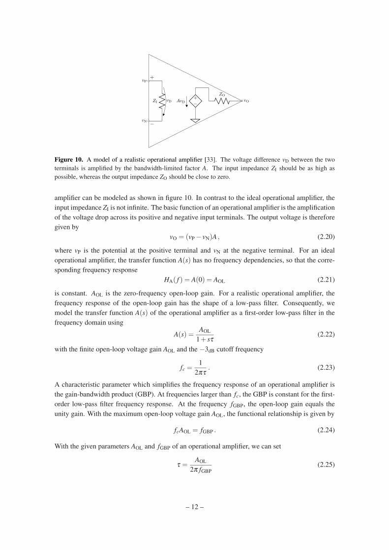
vP
vN
ZI vD
+
−
+
−AvD
ZO
vO
Figure 10. A model of a realistic operational amplifier [33]. The voltage difference vD between the twoterminals is amplified by the bandwidth-limited factor A. The input impedance ZI should be as high aspossible, whereas the output impedance ZO should be close to zero.
amplifier can be modeled as shown in figure 10. In contrast to the ideal operational amplifier, theinput impedance ZI is not infinite. The basic function of an operational amplifier is the amplificationof the voltage drop across its positive and negative input terminals. The output voltage is thereforegiven by
vO = (vP− vN)A , (2.20)
where vP is the potential at the positive terminal and vN at the negative terminal. For an idealoperational amplifier, the transfer function A(s) has no frequency dependencies, so that the corre-sponding frequency response
HA( f ) = A(0) = AOL (2.21)
is constant. AOL is the zero-frequency open-loop gain. For a realistic operational amplifier, thefrequency response of the open-loop gain has the shape of a low-pass filter. Consequently, wemodel the transfer function A(s) of the operational amplifier as a first-order low-pass filter in thefrequency domain using
A(s) =AOL
1+ sτ(2.22)
with the finite open-loop voltage gain AOL and the −3dB cutoff frequency
fc =1
2πτ. (2.23)
A characteristic parameter which simplifies the frequency response of an operational amplifier isthe gain-bandwidth product (GBP). At frequencies larger than fc, the GBP is constant for the first-order low-pass filter frequency response. At the frequency fGBP, the open-loop gain equals theunity gain. With the maximum open-loop voltage gain AOL, the functional relationship is given by
fcAOL = fGBP . (2.24)
With the given parameters AOL and fGBP of an operational amplifier, we can set
τ =AOL
2π fGBP(2.25)
– 12 –

and by setting s = jω with ω = 2π f , the transfer function of the open-loop gain for periodicsinusoidal signals is
A(j2π f ) =AOL
1+ j ffGBP
AOL. (2.26)
The frequency-dependent gain GA( f ) and phase shift ΦA( f ) are derived from Eq. 2.26.
GA( f ) = |A(j2π f )|= AOL√1+(
ffGBP
AOL
)2(2.27)
ΦA( f ) = ∠A(j2π f ) =−tan−1(
ffGBP
AOL
)(2.28)
0 fc
fGBP
Frequency f / Hz
0
AOL
Gai
n G
A(f
) / d
B
0 fc
fGBP
Frequency f / Hz
-90
-60
-30
0P
hase
shi
ft )
A(f
) / d
eg
Figure 11. The gain GA( f ) and the phase shift ΦA( f ) of the frequency response of an operational amplifierwith zero-frequency gain AOL. The frequency response is modeled as a first-order low-pass filter with thecutoff frequency fc =
fGBPAOL
. The attenuation of AOL is −20dB/decade above fc.
3. Circuit design of a charge-sensitive preamplifier
As briefly described in sec. 2.5, an operational amplifier integrates a charge, as there is a capacitorCF in the feedback and the time constant of the RFCF network is large compared to the drift time ofthe moving charge at its input. In general, a two-terminal equivalent circuit adequately representsthe feedback circuit. Thus, the RFCF network is summarized with the impedance ZF. In accordancewith figure 2, the impedance of the detector is modeled with the two-terminal impedance ZD.Both impedances are connected to the inverting terminal of the operational amplifier. In addition,there are parasitic shunt impedances between the negative and the positive input terminal of theoperational amplifier. As they are in parallel with the impedance of the detector, all additionalshunt impedances are absorbed by the model of ZD. For a simplified circuit analysis, the positiveterminal of the operational amplifier is grounded. If the operational amplifier requires a singlesupply operation, the positive terminal is biased towards the desired potential for the virtual ground.For a circuit analysis, this is negligible. Therefore, the initial circuit for the analysis is shown infigure 12.
– 13 –

−
+vOvP
vN
ZD
iZD
ZF
iZF
i
iInvOut
Figure 12. An operational amplifier with a current input and a voltage feedback connected to the negativeinput terminal. With ZF = CF||RF, this configuration is used for the charge-to-voltage amplification. ZD
represents all impedance connected between the input iIn and ground (e.g. capacitance of the detector andparasitic capacitance of the negative input terminal).
3.1 Circuit analysis
Kirchhoff’s current law is used for the fundamental circuit analysis. For the node at the negativeterminal of the operational amplifier, the sum of all currents must be zero.
0 = i− iZD + iZF (3.1)
Further, the currents can be expressed in terms of the feedback impedance ZF and shunt impedanceZD.
iZF =(vO− vN)
ZF(3.2)
iZD =vN
ZD(3.3)
According to eq. 2.20, and setting vP = 0, the voltage vN in eqs. 3.2 and 3.3 can be substituted with
vN =−vO
A. (3.4)
The solution of eq. 3.1 with eqs. 3.2-3.4 results in the current-to-voltage transfer function
−vO
i=
AZDZF
ZD(A+1)+ZF, (3.5)
where A is the transfer function of the operational amplifier according to eq. 2.22. Another usefulmethod for the circuit analysis is the principle of superposition. Because the system can be de-scribed with linear equations, a superposition of all current and voltage sources is possible. Thatmeans that first, if the current source for i is turned off (replaced with an open circuit), the volt-age source for vO is acting alone and the resulting voltage at the negative input terminal of theoperational amplifier is
vN|i=0 = vOZD
ZD +ZF. (3.6)
– 14 –

Second, if the voltage source vO is turned off (replaced with a short), the current source is actingalone and the voltage at the negative input terminal of the operational amplifier is
vN|vO=0 = iZDZF
ZD +ZF(3.7)
Finally, the superposition for the voltage node vN is the sum of eqs. 3.6 and 3.7
vN = vN|i=0 + vN|vO=0 . (3.8)
By inserting eqs. 3.4, 3.6 and 3.7 into eq. 3.8, the output voltage vO can be rewritten as
vO =−A(
vOZD
ZD +ZF+ i
ZDZF
ZD +ZF
). (3.9)
The derived eq. 3.9 is the same as eq. 3.5, but shows the terms for the basic block structure shownin figure 13 in an intuitive and easily readable form.
ZDZF
ZD+ZFΣ A
ZD
ZD+ZF
i vI − vD vO
−
Figure 13. Block diagram of the closed-loop transfer function. This structure shows the voltage feedbacknetwork and loop gain, which are essential for a stability analysis.
The basic block structure is used to identify the voltage feedback and the stability of the loop.It is obvious that the feedback network β is
β =ZD
ZD +ZF(3.10)
and the closed-loop voltage gain G is only [33]
G =A
1+Aβ=−vO
vI. (3.11)
The closed-loop gain G becomes 1β
if the loop gain Aβ is much greater than one. On the contrary,the closed-loop gain becomes infinite if the loop gain Aβ = −1. At this frequency, the systemtends to be unstable, and oscillates. As A and β are defined to have positive real values, the casewhere the loop gain becomes −1 only occurs if the loop gain is 1 and a phase shift of 180 isintroduced by the frequency response of the Aβ . A phase shift of a sinusoidal signal with 180 isequal to a multiplication with −1. To make the feedback circuit stable, the phase shift thereforehas to be less than 180 at the frequency fi, where the loop gain is 1. A sufficient phase marginat the frequency fi is required to ensure a stable operation over the entire temperature range, andalso to cover tolerances of the used integrated circuits. The example in figure 14 is calculatedwith the parameters from table 1 for the OPA657. The feedback impedance was chosen to be100fF in parallel with 25MΩ. Further, the detector capacitance of 6.7pF in parallel with a 50GΩ
– 15 –

100 101 102 103 104 105 106 107 108 109
Frequency / Hz
010203040506070
Mag
nitu
de /
dB
fi = 13 MHz
Open-loop gain AFeedback 1/-Loop gain A-
100 101 102 103 104 105 106 107 108 109
Frequency / Hz
-180
-150
-120
-90
-60
-30
0
Pha
se /
deg
Phase marginOpen-loop gain AFeedback 1/-Loop gain A-
Figure 14. The Bode plot of the closed-loop transfer function. The loop gain is 1 at the frequency fi with aphase margin of roughly 90. This is sufficient for a stable operation. See text for numerical values of theexample.
resistor and the parasitic input capacitance of 5.2pF are the shunting impedance ZD. The stabilityis investigated at the frequency, where the loop gain is 1. Mathematically, this intersection can becalculated by solving
|A(j2π f )β (j2π f )|= 1 . (3.12)
From the Bode plot shown in figure 14, this point can be found at
log(|A|)− log(| 1β|) = 0 . (3.13)
In this plot, the reciprocal of the feedback network β intersects the open-loop gain at approximately13MHz. At this frequency, the phase shift of the loop gain is 88, resulting in a phase margin φ of92, which is sufficient for a stable operation. The phase margin φ is calculated by
φ = 180− (∠A(2π fi)+∠β (2π fi)) . (3.14)
Besides the stability of the circuit, the effective input impedance also depends on the open-loop voltage gain of the amplifier, and is changed by the feedback network [33]. The effective inputimpedance of the CSA should be very low, to make sure that all current flows into the amplificationcircuit. Regarding figure 12, the effective input impedance from the CSA is defined by the ratio ofthe voltage at the input terminal iIn and the input current i. The voltage at the input terminal is vN,so the effective input impedance Z∗I is
Z∗I =vN
i. (3.15)
– 16 –

Solving eq. 3.1 for vN with eqs. 3.2-3.4, Z∗I can be expressed as
Z∗I =ZDZF
ZD(A+1)+ZF. (3.16)
As A becomes infinitely large, as we assume for an ideal operational amplifier, the effective inputimpedance is zero. This satisfies the principle of the virtual ground. If we assume an ideal detectorwithout a parasitic impedance from the CSA, ZD is infinite. For this case, the effective inputimpedance
limZD→∞
Z∗I =ZF
A+1(3.17)
is determined by the open-loop gain and the feedback network ZF. To force the CSA, so thatall current is integrated on the feedback capacitor, the impedance from eq. 3.17 must be smallcompared to the shunting impedance ZD.
3.2 Charge-to-voltage transfer function
The CSA is designed to measure a charge with a voltage output signal, where the peak amplitudeis proportional to the charge at the input. The relation of the output voltage vO to the input chargeQ is the charge-to-voltage transfer function
vO
Q= HQ . (3.18)
As the charge is defined to bedQdt
= i , (3.19)
where i is the electrical current, the corresponding Laplace transformation of eq. 3.19 is
L
Q′(t)= sQ(s) = i(s) . (3.20)
If we replace i in the current-to-voltage transfer function from eq. 3.5 by eq. 3.20 and set thefeedback network ZF =
1sCF
and parasitic impedance ZD = 1sCD
to single capacitors, then the charge-to-voltage transfer function is given by
HQ =−A
CD +CF(A+1). (3.21)
The simplification of the impedances to single capacitors is valid, as we want to investigate thefrequency response of the charge-to-voltage conversion. If the feedback time constant is chosenappropriately according to eq. 2.18, there is no significant peak amplitude loss in the voltage signal.The peak amplitude of the voltage signal is therefore independent of the feedback resistor RF. Theimpedance ZD can also be simplified for this analysis, as the equivalent input resistance of theamplifier and detector is much larger than the effective input impedance according to eq. 3.16.For an ideal operational amplifier with infinite open-loop gain A, HQ from eq. 3.21 becomes −1
CF
over the entire frequency domain. Since the open-loop voltage gain of an operational amplifier isnot independent of frequency, a more realistic charge-to-voltage transfer function is obtained byreplacing A from eq. 3.21 by eq. 2.22
HQ(s) =−AOL
CD +CF(AOL +1)+ sτ(CD +CF). (3.22)
– 17 –

The charge-to-voltage gain is then given by
|HQ(j2π f )|= GQ( f ) =AOL√
(CD +CF(AOL +1))2 +(
ffGBP
AOL(CD +CF))2
. (3.23)
The steady state of the system is derived by calculating the zero-frequency gain:
GQS = limf→0
GQ( f ) =AOL
CD +CF(AOL +1). (3.24)
Eq. 3.24 shows that a finite open-loop gain AOL attenuates the measured peak voltage. The mea-sured fraction of charge as a ratio of GQS over the ideal charge-to-voltage gain 1
CFis given by
GQSCF =AOL
CDCF
+AOL +1. (3.25)
It is obvious that the measured peak amplitude is decreased by an increased detector capacitance CD
or a reduced open-loop voltage gain AOL. Thus, the operational amplifier should provide a highand stable open-loop voltage gain for an improved system performance as illustrated in fig 15.
0 100 200 300 400 500 600 700 800 900C
D / C
F
50
60
70
80
90
100
Fra
ctio
n G
QSC
F /
%
AOL
= 1A
OL = 80 dB
AOL
= 70 dB
AOL
= 60 dB
Figure 15. The measured fraction of charge dependent on the ratio of input capacitance CD over feedbackcapacitance CF. The fraction is increased with an increased zero-frequency open-loop voltage gain AOL ofthe operational amplifier.
An equally important parameter of the CSA is the rise time of the output voltage as a reactionof a charge step at its input. As shown by eq. 2.12, the rise time is proportional to the cutofffrequency of the system. Therefore, to determine the rise time, we have to calculate its cutofffrequency, which is derived using eq. 3.23
|HQ(j2π fc)||HQ(0)|
=1√2
(3.26)
fc = fGBP
CDCF
+(AOL +1)
AOL(CDCF
+1). (3.27)
Eq. 3.27 shows, that the upper bandwidth limit is lowered with an increased fraction of the shuntingcapacitance CD over CF. The bandwidth is extended with a lower value of AOL, but this will reduce
– 18 –

the measured fraction of charge, as shown in figure 15. This also means that the signal-to-noiseratio is decreased and therefore, the resolution of the charge measurement is also decreased. AOL
should therefore be as large as possible. For this assumption, the bandwidth of the CSA is
limAOL→∞
fc =fGBP
CDCF
+1. (3.28)
Eq. 3.28 shows that the cutoff frequency and therefore the rise time of the CSA are directly propor-tional to the gain-bandwidth product of the amplifier. The response of the transfer function fromeq. 3.21 to a unit step is shown in figure 16.
0 20 40 60Time / ns
0
0.2
0.4
0.6
0.8
1
Cha
rge
/ As
AOL
= 1, CD
/CF = 10
AOL
= 1, CD
/CF = 100
AOL
= 60 dB, CD
/CF = 100
Figure 16. The output signal of the charge-sensitive amplifier with a unity step at its input. The rise timeis increased with an increasing ratio of CD
CF. The gain-bandwidth product of the operational amplifier was
assumed to be fGBP = 1GHz. In this example, the rise times are 17ns (solid line), 32ns (dashed line)and 35ns (dotted line). The decreased rise time related to a smaller open-loop gain AOL is caused by theattenuation of the peak amplitude.
3.3 Input coupling of the CSA
As shown in figure 3, at least one of the electrodes is biased at a negative high voltage. Thus,the amplifier at the cathode must be protected against the bias voltage, since it is not commonfor integrated circuits to operate at high input voltages in the range of several hundreds of volts.A capacitor in series to the amplifier input blocks the bias voltage of the detector, but allows thedetector current to flow. This electrical circuit is shown in figure 17, where the coupling capacitorCB is represented by the impedance ZB. In this configuration, the parasitic impedance ZI andthe detector impedance ZD are separated by the impedance ZB. As the influence of the couplingcapacitor is not apparent at first glance throughout the equation for the current-to-voltage transferfunction, a calculation with an infinite loop gain turns out the simplified equation
−vO
i=
ZDZF
ZB +ZD. (3.29)
To eliminate the influence of the impedance ZB, it must be much smaller than ZD. Where allimpedances are represented by a single capacitor, the steady-state charge-to-voltage gain is ulti-mately given by
vO
Q=
1
CF
(1+ CD
CB
) . (3.30)
– 19 –

−
+vOvP
vN
ZI
iZI
ZF
iZF
i
iInvOut
ZD
iZD
ZB
iZB
Figure 17. A functionally equivalent configuration to figure 12 for the charge-to-voltage amplification. Theinput impedance at the terminal iIn is a Pi network instead of the single impedance ZD. ZB is a high-voltagecoupling capacitor to protect the low-voltage input terminals of the operational amplifier.
Eq. 3.30 shows that the coupling capacitor must be much larger than the detector capacitance toavoid a peak amplitude loss, thus reducing the signal-to-noise ratio.
3.4 Noise
As has been pointed out, the noise caused by the electronics and the corresponding signal-to-noiseratio (SNR) characterize the quality of the CSA with respect to the achievable energy resolution.The precision of the charge measurement and the achievable timing are directly related to the SNR.Regarding both values, the front-end electronics should not limit the intrinsic resolution of thedetector. Thus, to reduce the electronics noise, the noise sources of the detector system must beidentified in the first step. The main source for the electronics noise is the operational amplifier.But the passive components of an electronic circuit also generate noise. The resulting noise at theoutput is the sum of all noise sources at the input, amplified by the noise gain. The essential noisesources of the electronics circuit are shown in figure 18. The noise contribution of the operational
−
+vOvP
vN
inA
+ −
vnA
inRF
vOut
inDinRB
iIn
Figure 18. The charge-sensitive amplifier configuration with its dominant noise sources at the input terminaliIn. For the noise analysis, the current noise sources from the bias resistor (inRB ), equivalent resistor of thedetector (inD ), feedback resistor (inRF ), and amplifier (inA ) can be substituted by a single source, as they actin parallel. Finally, the noise analysis is made with a current noise source in in parallel (parallel noise) and avoltage noise source vn in series (series noise) to the input terminal.
– 20 –

amplifier is simplified to a model, where its noise is characterized by an equivalent voltage noisesource vnA and current noise source inA at the inverting input terminal. Additionally, all resistors inthe system contribute to the total noise by adding thermal noise. The equivalent noise current of aresistor at temperature T is given by
inR =4kT
R(3.31)
where k is the Boltzmann constant [21]. The equivalent resistor RD of the detector, the biasingresistor RB, and the equivalent resistor RF of the feedback impedance contribute to the total noisefollowing eq. 3.31. Each is represented by a current source in figure 18. As there are multiple noisesources in the system, they can all be absorbed into a single source for the voltage noise vn and asingle source for the current noise in with
in = inRD + inRB + inRF + inA , (3.32)
as they are connected in parallel. Voltage noise sources can be summed, as they are connectedin series. As we assume that all noise sources have a flat frequency spectrum (white noise), theresulting noise spectral density at the output is shaped by the noise transfer function (noise gain).
The noise spectral density is usually expressed in units of nV√Hz
. With regard to the blockdiagram of the closed-loop transfer function from figure 13, the current noise source is amplifiedby the current-to-voltage transfer function, whereas the voltage noise source is amplified by theclosed-loop voltage gain. As illustrated in figure 19, the input noise current in to output noise
ΣZDZF
ZD+ZFΣ A
ZD
ZD+ZF
i vI − vD vO
−
vn−
in
Figure 19. Block diagram of the closed-loop transfer function with additional current noise source in andvoltage noise source vn. Both sources act at the negative input terminal of the operational amplifier but havedifferent transfer functions.
voltage vOn transfer function Gin is given by eq. 3.5 and the input noise voltage vn to vOn transferfunction Gvn is given by eq. 3.11.
For a clear view on the components of the resulting spectral noise density in figure 20, thecalculations are based on the ideal model of the CSA. Figure 20 shows the contribution of the inputcurrent noise, which has a typical 1
f shape and dominates the low frequency range (referred to asflicker noise). The noise density in the upper frequency range is dominated by the input voltagenoise but remains flat. If the open-loop gain is sufficiently large, the voltage noise is amplifiedby the factor 1
β. A more realistic noise spectral density is shown in figure 21. This illustration
emphasizes the impact of the feedback resistor RF and the gain-bandwidth product fGBP. Thedensity of the flicker noise is limited in its upper value. It has the shape of a typical low-pass filter,which is determined by the time constant RFCF of the feedback impedance. The component relatedto the voltage noise has the spectral density of a band-pass filter, where the upper-corner frequency
– 21 –

fI
Frequency / Hz
vn/-
Noi
se d
ensi
ty /
(nV
Hz-1
/2)
vnGvn = vn
3CD
CF+ 1
4
inGin =in
2:fCF
vOn =
q(vnGvn)
2 + (inGin)2
Total noise densityVoltage noise densityCurrent noise density
Figure 20. The noise spectral density log-log plot for the ideal charge-sensitive amplifier with the capacitorCF in the feedback network and the capacitor CD at its input terminal. In the lower frequency range, thenoise density is dominated by the current noise. Above the frequency fI, the portion of the voltage noisedominates the total noise density vOn.
fL1
fL2
fI
fC
Frequency / Hz
vn
vn/-
RFin
Noi
se d
ensi
ty /
(nV
Hz-1
/2)
fL1 =1
2:RF (CD + CF)
fL2 =1
2:RFCF
fI =
q(RFin)
2! v2
n
vn2:RF (CD + CF)
fC =fGBP
CD
CF+ 1
Total noise densityVoltage noise densityCurrent noise density
Figure 21. The noise spectral density log-log plot for the charge-sensitive amplifier with the resistor RF andcapacitor CF in the feedback network and the capacitor CD at its input terminal. The frequency responseof the current noise density has the shape of a low-pass filter, whereas the voltage noise density has theresponse of a band-pass filter. The time constant τ = RFCF determines the low cutoff frequency fL2 for bothresponses. The voltage noise density is limited by the corner frequency fc. Thus, the total noise density isbounded over the whole frequency range.
fc is limited by the gain-bandwidth product and the detector capacitance CD. At zero frequency,the voltage noise is limited to the value of vn.
The noise spectral density determines the root-mean-square amplitude of the output noise(rms noise) over a given bandwidth. As the noise spectral density is bounded over the entirefrequency range, the total rms noise Vrms is calculated by
Vrms =
√∫∞
0(vnGvn)
2 +(inGin)2d f (3.33)
An additional signal processing with filters (pulse shapers) must be adapted in accordance to thenoise spectral density.
– 22 –
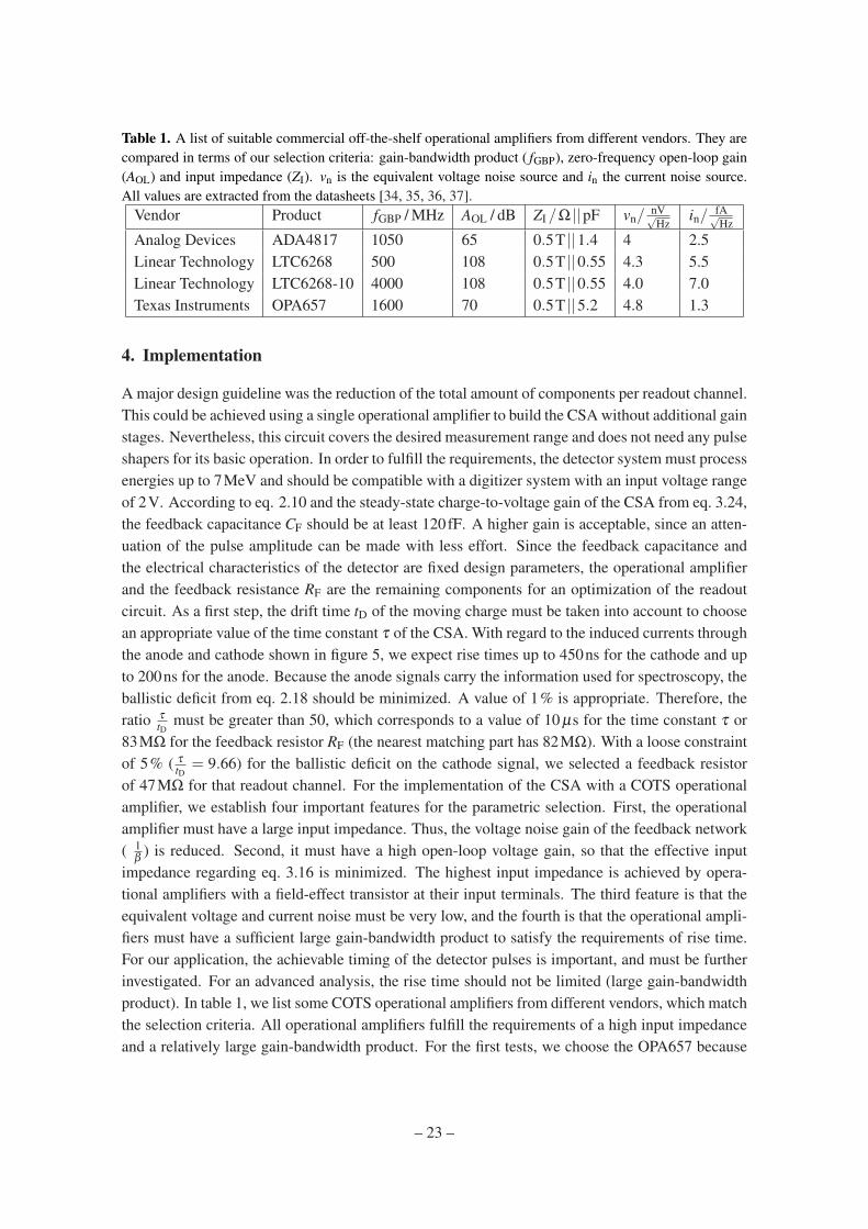
Table 1. A list of suitable commercial off-the-shelf operational amplifiers from different vendors. They arecompared in terms of our selection criteria: gain-bandwidth product ( fGBP), zero-frequency open-loop gain(AOL) and input impedance (ZI). vn is the equivalent voltage noise source and in the current noise source.All values are extracted from the datasheets [34, 35, 36, 37].
Vendor Product fGBP / MHz AOL / dB ZI /Ω ||pF vn/nV√Hz
in/ fA√Hz
Analog Devices ADA4817 1050 65 0.5T ||1.4 4 2.5Linear Technology LTC6268 500 108 0.5T ||0.55 4.3 5.5Linear Technology LTC6268-10 4000 108 0.5T ||0.55 4.0 7.0Texas Instruments OPA657 1600 70 0.5T ||5.2 4.8 1.3
4. Implementation
A major design guideline was the reduction of the total amount of components per readout channel.This could be achieved using a single operational amplifier to build the CSA without additional gainstages. Nevertheless, this circuit covers the desired measurement range and does not need any pulseshapers for its basic operation. In order to fulfill the requirements, the detector system must processenergies up to 7MeV and should be compatible with a digitizer system with an input voltage rangeof 2V. According to eq. 2.10 and the steady-state charge-to-voltage gain of the CSA from eq. 3.24,the feedback capacitance CF should be at least 120fF. A higher gain is acceptable, since an atten-uation of the pulse amplitude can be made with less effort. Since the feedback capacitance andthe electrical characteristics of the detector are fixed design parameters, the operational amplifierand the feedback resistance RF are the remaining components for an optimization of the readoutcircuit. As a first step, the drift time tD of the moving charge must be taken into account to choosean appropriate value of the time constant τ of the CSA. With regard to the induced currents throughthe anode and cathode shown in figure 5, we expect rise times up to 450ns for the cathode and upto 200ns for the anode. Because the anode signals carry the information used for spectroscopy, theballistic deficit from eq. 2.18 should be minimized. A value of 1% is appropriate. Therefore, theratio τ
tDmust be greater than 50, which corresponds to a value of 10 µs for the time constant τ or
83MΩ for the feedback resistor RF (the nearest matching part has 82MΩ). With a loose constraintof 5% ( τ
tD= 9.66) for the ballistic deficit on the cathode signal, we selected a feedback resistor
of 47MΩ for that readout channel. For the implementation of the CSA with a COTS operationalamplifier, we establish four important features for the parametric selection. First, the operationalamplifier must have a large input impedance. Thus, the voltage noise gain of the feedback network( 1
β) is reduced. Second, it must have a high open-loop voltage gain, so that the effective input
impedance regarding eq. 3.16 is minimized. The highest input impedance is achieved by opera-tional amplifiers with a field-effect transistor at their input terminals. The third feature is that theequivalent voltage and current noise must be very low, and the fourth is that the operational ampli-fiers must have a sufficient large gain-bandwidth product to satisfy the requirements of rise time.For our application, the achievable timing of the detector pulses is important, and must be furtherinvestigated. For an advanced analysis, the rise time should not be limited (large gain-bandwidthproduct). In table 1, we list some COTS operational amplifiers from different vendors, which matchthe selection criteria. All operational amplifiers fulfill the requirements of a high input impedanceand a relatively large gain-bandwidth product. For the first tests, we choose the OPA657 because
– 23 –

of its larger open-loop gain and bandwidth in comparison to the ADA4817. For the second part, wechoose the LTC6268-10 because of its outstanding parameters and very low parasitic capacitance.Both operational amplifiers are available in an almost pin compatible package. Consequently, theevaluation procedure can be done with the same hardware. After a first attempt with the LTC6268,which runs on the OPA657 PCB layout, we decided to populate the hardware with the LTC6268-10; unfortunately, this circuit tends to oscillate, as also observed in [31]. Thus the implementationof the CSA with the OPA657 shows the best performance for the first prototype (see figure 22).
Figure 22. The detector assembly with unpopulated readout boards (left) and a close-up of a populatedprinted circuit board with 17 charge-sensitive amplifiers (right).
Despite the higher parasitic input capacitance, a great advantage of the OPA657 over theLTC6268 is its wide supply voltage range of 12V. This provides a larger headroom for pulsepile-ups until the output voltage of the amplifier saturates. Thus, this amplifier is best-suited forhigh count rates with high energies. Nevertheless, the count rate capability mainly depends on thesignal processing system, which is limited by the input voltage range of the digitizer and the digitalpulse processing system [38]. Moreover, any rate limitations must be determined by field experi-ments. The readout board contains 17 CSAs, where one anode channel is equipped with a test pulseinput and another channel is dedicated to the readout of the cathode. All necessary functionality,including low voltage power supply, high voltage filters, biasing, and decoupling capacitors, is in-cluded on the PCB. Each CSA has a passive low-pass filter at its output. The bandwidth is limitedto 21.654MHz (16.15ns rise time), which is sufficient for the CZT detector signals. One channelof the readout board is used for the evaluation of the CSA and contains a test input circuit. Thiscircuit consists of a termination resistor and a series capacitor of 0.3pF± 0.05pF for the chargeinjection in accordance with [32]. The theoretical performance parameters of the CSA are listed intable 2. These values are estimates and will be verified with experimental results.
5. Results
The readout board is evaluated with the test pulse input and with the detector shown in figure 2.The test pulse input is sourced by a signal generator with a step voltage input. According to thecurrent-voltage relation of a capacitor, the step voltage applied to test input capacitor generates a
– 24 –

Table 2. Numerical estimation of the electrical characteristics of the different readout channels. The calcu-lations refer to a CSA based on the OPA657. The value of the equivalent noise charge (ENC) is given inunits of the elementary charge e.
Cathode Anode (Pixel) Test inputRF ||CF 47MΩ || 100fF 82MΩ || 100fF 82MΩ || 100fF
CDCF
119 53.05 55Ballistic deficit 95.36% 98.79% 99.9%Charge fraction 96.34% 98.32% 98.26%
Steady-state gain 9.19 VpC 9.71 V
pC 9.82 VpC
Cutoff frequency 13.84MHz 30.11MHz 29.08MHzRise time 25.27ns 11.61ns 12.03ns
Noise level (rms) 2.62mV 1.82mV 1.80mVNoise level (rms), BW limited 2.01mV 1.26mV 1.21mV
ENC (rms), BW limited 1365e 810e 769ePeak amplitude at 511keV in CZT 162.11mV 171.38mV 173.33mV
current flowing into the CSA. With a varying shape of the voltage signal, arbitrary detector signalscan be synthesized.
5.1 Test pulse input
The most important feature of the front-end electronics is the noise performance. There are variousmethods to analyze the noise of a linear time-invariant (LTI) system like the CSA. A commonmethod is described in the IEEE Std 1241-201, referred to as "Sine-wave testing and fitting" [39].It is known that the response of an LTI system to a pure sine-wave is a sine-wave with the samefrequency, but potentially different amplitude and phase. Tests with a sine-wave have the advantagethat the waveform can be generated very accurately and the interpretation is done by standardizedinstruments and tools. If a sine-wave is applied to the input, the output depends on the transferfunction of the system and is superimposed with noise. The input sine-wave is derived a posterioriby a four-parameter sine-wave fit, and the residual is the noise level, as described in [39]. Thewaveform is captured by our digitizer with 100MSPS and 14bit resolution. The digitizer boardprovides an SNR of 71.3dB at around −1dB of full scale input (2.3Vpp). This corresponds toan rms noise level of 201 µV. These values are measured at an input frequency of 2MHz. Withthe same setup, the sine-wave test with the test input of the CSA results in an rms noise level of1.24mV. The result is shown in figure 23. This is in accordance with the predicted values in table 2for the test input.
Moreover, other tests were made to validate the pulse shape at the output of the CSA. Thesignal generator was set up to generate a step input with a rise time of approximately 8ns. Figure 24shows the output signals for a variation of the input amplitude AT. The fit of the peak heights andthe input shows an excellent linearity, with a maximum deviation of 2mV. The linear fit results ina gain of 3.05, which correlates with the ratio of test input capacitance over feedback capacitance.
The test pulse input was also used to evaluate the timing capabilities of the CSA. As before, thesignals were captured with the digitizer and processed offline. The test pulses were synchronized to
– 25 –

0 100 200 300 400 500Time mod T / ns
-4
-2
0
2
4"
Sin
efit
/ mV
-3 -2 -1 0 1 2 3 4"Sinefit / mV
0
0.2
0.4
0.6
0.8
1
Nor
mal
ized
cou
nts
/ a.U
.
"Sinefit7 = 3.357 7V< = 1.238 mVN = 16k
Figure 23. Noise measurement of the charge-sensitive amplifier with a sine-wave test. A 2MHz sine-wavewas applied to the test input and the difference between the output signal and a four-parameter sine-wave fit(∆Sinefit) is plotted against the period T of the sine-wave (left). All harmonic distortions were eliminatedby the test procedure, revealing the noise level (standard deviation σ of ∆Sinefit, right).
0 5 10 15 20 25 30 35 40Time / 7s
0
50
100
150
200
250
300
Out
put /
mV
AT = 7 mV
AT = 55 mV
AT = 100 mV
0 0.1 0.2 0.3 0.4 0.5 0.57Test pulse amplitude A
T / V
0
0.5
1
1.5
2
Pul
se h
eigh
t / V
Linear fitMeasurement
Figure 24. A measurement with different rectangular pulses with amplitudes AT injected to the test inputcapacitance. The output signal was recorded with the 100MSPS digitizer (left). Each pulse height is therms value of 1k events (right). The linearity error is in the range from −2mV to 1.5mV.
a known timing reference signal (sine-wave signal). The timing performance was obtained from thedifference between the zero crossing point of the sine-wave and a digital constant fraction trigger(fraction= 0.2) on the output signal of the CSA. Both timestamps were calculated by software. Theresults of the timing measurement are shown in figure 25. At high signal amplitudes, the timingperformance is in the range of several picoseconds (32ps standard deviation). This value increaseswith lower signal amplitudes, because the SNR decreases as well. This rough estimate of timingperformance shows that the CSA does not limit the timing performance of the CZT detector, whichis estimated to be in a range of some nanoseconds [40].
5.2 Pixel detector
The performance of the CSA is finally evaluated with the Redlen pixel detector and the hardwareshown in figure 22. The detector is biased at −600V and the signals are captured with the digi-tizer. The waveforms of a single pixel and the cathode are stored for an offline analysis. The firsttest should measure the energy on both electrodes dependent on the depth of interaction (DOI).As shown in figure 4, the relationship between the DOI and the weighting potentials should beexperimentally verified with the data from the detector. The DOI is measured either by the ratio ofcathode-over-anode energy [41] or by a direct measurement of the drift time of the moving charge.The drift time of charge correlates with the rise time of the CSA [42]. For our analysis, we calcu-
– 26 –

-218 -106 6 118 230 342"t / ps
291
292
293
294
295
296
297P
ulse
hei
ght /
mV
0.1
0.3
0.5
0.7
0.9
-72 -48 -24 0 24 48 72"t / ps
2221
2222
2223
2224
2225
2226
2227
2228
Pul
se h
eigh
t / m
V
0.1
0.3
0.5
0.7
0.9
Figure 25. Results of about 1k timing measurements with the 100MSPS digitizer. The pulse height is themaximum value of the output from the charge-sensitive amplifier. The time ∆t is the difference between thepulse trigger and the timing reference from the signal generator. The standard deviation of the measurementsare σx = 131ps and σy = 1.15mV for the left plot and σx = 32ps and σy = 1.21mV for the right plot. Thecolormap is in logarithmic scale.
late the rise time as the time difference between two thresholds of the rising edge of the signal. Onboth the cathode and the anode signal, we set the thresholds to 10% and 90% of the peak ampli-tude. The data was collected with a 22Na radioactive source and an arbitrary selected pixel of the2 × 2 center array. The anode was used to trigger an event while the cathode signal was capturedat the same time. This measurement shows the expected relationship of the DOI and the measured
Figure 26. Measurement of a 22Na radioactive source with the Redlen CZT detector and the charge-sensitiveamplifier (CSA) readout board. The peak amplitudes of the output pulses from the CSA are plotted againstthe 10% − 90% rise times. The weighting potentials of the cathode (left) and an anode (right) are clearlyvisible along the 511keV photopeak (158mV for the cathode and 182mV for the anode at rise times of410ns and 200ns).
cathode and anode energy. The peak amplitude of the 511keV photopeak of the cathode decreaseslinearly in correlation with the rise time. Events near the cathode cause the long rise times. Thelinear shape matches the expected weighting potential of the cathode. The pulse height of the anode
– 27 –

Table 3. Measured parameters of the readout electronics. All channels are bandwidth-limited to about21.654MHz by a passive RC low-pass filter. If appropriate, the standard deviation σ is noted for the mea-sured value.
Parameter Measured value Channel CommentRise time 10%−90% 14.86ns,
σ = 371psTest input Input pulse: 3.0ns fall time,
Vout : 2Vpp
Noise level (rms) 1.24mV Test input Sine-wave testτ1 (82MΩ || 100fF) 8.091 µs,
σ = 86nsCathode Waveform fit: f (t) = e−t/τ1
τ2 (47MΩ || 100fF) 4.964 µs,σ = 181ns
Anode Waveform fit: f (t) = e−t/τ2
Peak amplitude at 511keV 158mV Cathode Pulse height at longest drift timePeak amplitude at 511keV 182mV Anode Pulse height at longest drift timeSteady-state gain 8.95 V
pC Cathode at 511keV with Ei = 4.64eVSteady-state gain 10.31 V
pC Anode at 511keV with Ei = 4.64eV
signal also decreases dependent on the calculated rise time. The DOI is clearly visible along thepredicted shape of the weighting potential, as shown in figure 4. The expected peak amplitudes forthe photopeak are in accordance with the calculated values in table 2. A summary of the measuredkey metrics for the CSA is given in table 3.
The correlation between the rise time of the cathode signal and the cathode-over-anode ratiois shown in figure 27. Both values carry information about the DOI. In contrast, the correlationbetween the cathode and anode rise time is smeared out. This is caused by uncertainties in thecrossing of the low-level threshold, because of the slow rising component of the anode signal at thebeginning. The low-level trigger is difficult to hit exactly without additional effort. However, the
Figure 27. Correlation of the cathode-over-anode ratio (CAR) with the measured rise times of the cathodepulses from the 22Na radioactive source measurement (left). The rise time has a strong correlation to theCAR and therefore to the depth of interaction (DOI) in the detector volume. The correlation of the anoderise time to the DOI is smeared out (right).
measurements show that the depth of interaction can be calculated by the rise time of the cathode
– 28 –

signal or the ratio of cathode-over-anode energy. In conclusion, the measurement of the cathoderise time is more precise than the anode rise time, because the cathode signal rises with a nearlylinear slope. An advantage of the rise time estimation is that the information is derived from onedetector signal instead of two. Additionally, the calculation of cathode-over-anode ratio is errorprone due to charge-sharing events.
It is evident that the anode energy has to be corrected dependent on the DOI. There are sev-eral approaches for the depth correction, which are all carried out empirically. The results areachieved with best-fit functions, based on e.g. polynomial [43] or exponential [44], [45] equations.Our approach is based on the weighting potential of a pixel, as this is the cause for the incorrectmeasurement. For depth correction, we select the events of the 511keV photopeak along its clusterwith reduced peak height and rise time, as shown in figure 28. A fit of the weighting potential
130 140 150 160 170 180 190Anode photopeak amplitude / mV
0
50
100
150
200
250
300
350
400
450
Ris
etim
e ca
thod
e / n
s
0 170 341 511 764 1062 1275Anode energy / keV
100
101
102
Cou
nts
22Na spectrum7 = 511 keV< = 9.5 keV
Figure 28. The 511keV photopeak along the signal rise time at the cathode with the corresponding datapoints used for the fit of the weighting potential (left). The corrected spectrum of the anode energy is inde-pendent of the depth of interaction (right). The selected pixel has an energy resolution of 9.5keV (standarddeviation) for the photopeak, which corresponds to 4.3%FWHM. The spectrum is recorded without anyadditional pulse shapers.
according to eq. 2.6 matches the data points. Thus, the derived mathematical relationship is usedto correct the anode energy, which is shown in figure 28. We also evaluated polynomial equa-tions for the fitting function, resulting in comparable results with a fourth-degree polynomial. Thepresented measurements were processes without any additional pulse shapers. This results in an
– 29 –

energy resolution of 4.3% (FWHM) for the 511keV photopeak. With the use of additional digitalpulse shapers [46], the energy resolution could be improved to 2.2% (see figure 29).
0 100170 341 511 764 1062 1275Anode energy / keV
100
101
102
Cou
nts
22Na spectrumwith shaper7 = 511 keV< = 4.8 keV
Figure 29. The results of a measurement with our charge-sensitive amplifier and the Redlen CZT detector.The use of an additional digital pulse shaper improves the energy resolution of the 511keV photopeak to4.8keV (standard deviation). This corresponds to 11keV FWHM (2.2%). All events of one pixel are shown.
6. Summary
This paper has presented a circuit design and implementation of the analog front-end electronicsfor a cadmium zinc telluride (CdZnTe, CZT) pixel detector. Starting from the electrical equivalentcircuit of the CZT, its electrical characteristics were discussed and a connection scheme presented.A short summary of the signal formation in a CZT pixel detector was provided, and the weightingpotentials of the electrodes shown. Finally, these equations were applied for an analysis of thedetector signals. After a comparison of different readout circuits, we focused our investigation onthe charge-sensitive amplifier for the readout of the detector signals. As an ASIC-based solutionis not available for the application with high gamma-ray energies and count rates, we designedthe front-end electronics for the 8 × 8 pixel detector with commercial off-the-shelf operationalamplifiers.
We have shown a detailed analysis of the charge-sensitive amplifier in conjunction with theelectrical model of the CZT detector. The limits of the design in terms of gain, bandwidth, andnoise were given with exact equations and numerical values. The performance of the readout elec-tronics was measured with synthesized detector signals from a test pulser and with a pixel detectorof size 20 × 20 × 5mm3 from Redlen. The measurements with the test pulse showed that therms noise level of 1.24mV is below the nominal intrinsic resolution of about 8keV (FWHM at122keV) of the detector. Furthermore, we have shown that the signal-to-noise ratio is also suffi-cient for a timing far below 1ns, which outstrips the expected CZT performance. All the resultshave been achieved without an additional pulse shaper. We also investigated the performance of thecharge-sensitive amplifiers with the detector from Redlen, and were able to verify that the claimeddepth dependence is in accordance with the calculated weighting potential of a pixel. We presented
– 30 –

a measurement of a 22Na radioactive source and showed a correction of the measured energy de-pendent on the depth of interaction. After depth correction, we obtain an energy resolution of about22keV (4.3% FWHM at 511keV). This result could be improved to 11keV (2.2%FWHM) by theuse of additional digital pulse shapers. Finally, the front-end electronics fulfill our requirementsand operate from several keV up to 7MeV with sub-nanosecond timing capabilities. The charge-sensitive front-end electronics were used in a multichannel digital signal processing system for aCompton camera prototype.
References
[1] S. Del Sordo et al., Progress in the development of CdTe and CdZnTe semiconductor radiationdetectors for astrophysical and medical applications, Sensors 9 (2009) 3491.
[2] L. Verger et al., Performance of a new CdZnTe portable spectrometric system for high energyapplications, IEEE Trans. Nucl. Sci. 52 (2005) 1733.
[3] C.G. Wahl et al., The Polaris-H imaging spectrometer, Nucl. Instr. Meth. A 784 (2015) 377.
[4] T. Kormoll et al., A prototype Compton camera for in-vivo dosimetry of ion beam cancer irradiation,IEEE NSS/MIC (2011) 3484.
[5] F. Hueso-González et al., Test of Compton camera components for prompt gamma imaging at theELBE bremsstrahlung beam, JINST 9 (2014) P05002.
[6] W. Lee et al., Mini Compton Camera Based on an Array of Virtual Frisch-Grid CdZnTe Detectors,IEEE Trans. Nucl. Sci. 63 (2016) 259.
[7] M. McCleskey et al., Evaluation of a multistage CdZnTe Compton camera for prompt γ imaging forproton therapy, Nucl. Instr. Meth. A 785 (2015) 163.
[8] J.C. Polf et al., Imaging of prompt gamma rays emitted during delivery of clinical proton beams witha Compton camera: feasibility studies for range verification, Phys. Med. Bio. 60 (2015) 7085.
[9] T. Taya et al., First demonstration of real-time gamma imaging by using a handheld Compton camerafor particle therapy, Nucl. Instr. Meth. A (2016).
[10] C. Golnik et al., Tests of a Compton imaging prototype in a monoenergetic 4.44 MeV photon field – abenchmark setup for prompt gamma-ray imaging devices, JINST 11 (2016) P06009.
[11] Z. He et al., 3-D position sensitive CdZnTe gamma-ray spectrometers, Nucl. Instr. Meth. A 422(1999) 173.
[12] B. Gan et al., A low-noise 64-channel front-end readout ASIC for CdZnTe detectors aimed to hardX-ray imaging systems, Nucl. Instr. Meth. A 816 (2016) 53.
[13] P. Födisch et al., Eine Ausleseelektronik für CZT-Detektoren mit dem RENA-3 IC von Nova R&D,104th Meeting of the Study Group for Electronic Instrumentation, SEI (2013).
[14] A. Schumann et al., Simulation and experimental verification of prompt gamma-ray emissions duringproton irradiation, Phys. Med. Biol. 60 (2015) 4197.
[15] F. Hueso-González et al., First test of the prompt gamma ray timing method with heterogeneoustargets at a clinical proton therapy facility, Phys. Med. Biol. 60 (2015) 6247.
[16] G. Pausch et al., Scintillator-Based High-Throughput Fast Timing Spectroscopy for Real-Time RangeVerification in Particle Therapy, IEEE Trans. Nucl. Sci. 63 (2016) 664.
– 31 –

[17] Y. Ramachers et al., Energy resolution improvement in room-temperature CZT detectors, JINST 2(2007) P12003.
[18] Redlen Technologies Inc., M1757 CZT Radiation Detector, Datasheet, 2011.
[19] P.H. Lu et al., Ruggedization of CdZnTe detectors and detector assemblies for radiation detectionapplications, Nucl. Instr. Meth. A 784 (2015) 44.
[20] S. Awadalla, Solid-State Radiation Detectors: Technology and Applications, CRC Press, 2015.
[21] H. Spieler, Semiconductor Detector Systems, Oxford University Press, 2005.
[22] A. Garson et al., Leakage Currents and Capacitances of Thick CZT Detectors, IEEE NSS (2007)2258.
[23] P. De Antonis et al., Measuring the bulk resistivity of CdZnTe single crystal detectors using acontactless alternating electric field method, Nucl. Instr. Meth. A 380 (1996) 157.
[24] L. Rossi et al., Pixel Detectors: From Fundamentals to Applications, Springer, 2006.
[25] iseg Spezialelektronik GmbH, High Voltage Power Supply, SHQ HIGH PRECISION series,Operator’s Manual, Rev. 2014-02-13-17-34.
[26] C. Grupen et al., Particle Detectors, Cambridge University Press, 2008.
[27] Z. He, Review of the Shockley-Ramo theorem and its application in semiconductor gamma-raydetectors, Nucl. Instr. Meth. A 463 (2001) 250.
[28] N. Wermes, Pixel Vertex Detectors, arXiv:physics/0611075, 2006.
[29] Z. He, Direct measurement of product of the electron mobility and mean free drift time of CdZnTesemiconductors using position sensitive single polarity charge sensing detectors, J. Appl. Phys. 84(1998) 5566.
[30] H.Y. Cho et al., Measurement of the drift mobilities and the mobility-lifetime products of chargecarriers in a CdZnTe crystal by using a transient pulse technique, JINST 6 (2011) C01025.
[31] G. Brisebois, Op Amp Combines Femtoamp Bias Current with 4GHz Gain Bandwidth Product, ShinesNew Light on Photonics Applications, LT Journal of Analog Innovation 25 (2015) 1.
[32] G.F. Knoll, Radiation Detection and Measurement, John Wiley & Sons Inc., 2010.
[33] P. Horowitz, The Art Of Electronics, Cambridge University Press, 1989.
[34] Analog Devices, ADA4817-1/ADA4817-2, 1 GHz FastFET Op Amps Data sheet Rev. B, 2013.
[35] Linear Technology, LTC6268/LTC6269 500MHz Ultra-Low Bias Current FET Input Op AmpData sheet 62689f, 2014.
[36] Linear Technology, LTC6268-10/LTC6269-10 4GHz Ultra-Low Bias Current FET Input Op AmpData sheet 626810f, 2015.
[37] Texas Instruments, OPA657 1.6-GHz, Low-Noise, FET-Input Operational AmplifierData sheet SBOS197F, 2015.
[38] L. Abbene et al., High-rate dead-time corrections in a general purpose digital pulse processingsystem, J. Synchrotron Rad. 22 (2015) 1190.
[39] IEEE Instrumentation & Measurement Society, IEEE Standard for Terminology and Test Methods forAnalog-To-Digital Converters, IEEE Std 1241-2000.
– 32 –

[40] L.J. Meng, Exploring the limiting timing resolution for large volume CZT detectors with waveformanalysis, Nucl. Instr. Meth. A 550 (2005) 435.
[41] W. Li et al., Experimental results from an Imarad 8×8 pixellated CZT detector, Nucl. Instr. Meth. A458 (2001) 518.
[42] L. Verger et al., New trends in γ−ray imaging with CdZnTe/CdTe at CEA-Leti, Nucl. Instr. Meth. A571 (2007) 33.
[43] B. Donmez et al., 3D position sensing on UltraPeRL CdZnTe detectors, IEEE NSS (2007) 420.
[44] J. Hong et al., Cathode depth sensing in CZT detectors, Proc. SPIE 5165 (2004).
[45] H.Y. Cho et al., Improvement of the energy resolution in a pixellated CdZnTe detector using depthsensing based on pulse rise-time correlation, JINST 11 (2016) C02081.
[46] P. Födisch et al., Digital high-pass filter deconvolution by means of an infinite impulse response filter,Nucl. Instr. Meth. A 830 (2016) 484.
– 33 –