charge generation by secondary particles from nuclear...
TRANSCRIPT
CHARGE GENERATION BY SECONDARY PARTICLES FROM NUCLEAR REACTIONS
IN BACK END OF LINE MATERIALS
By
Nathaniel Anson Dodds
Thesis
Submitted to the Faculty of the
Graduate School of Vanderbilt University
in partial fulfillment of the requirements
for the degree of
MASTER OF SCIENCE
in
Electrical Engineering
December, 2009
Nashville, Tennessee
Approved:
Professor Robert A. Reed
Professor Marcus H. Mendenhall

ii
ACKNOWLEDGEMENTS
More than anyone else, I am indebted to my wife Stacey for her support through these
years of research. From agreeing to move far from home (how far is Nashville from Phoenix?) to
encouraging me to finally write this thesis, she has been my sweet companion. I owe my parents
for teaching me to love learning, and for working so I could have more opportunities than they
ever had.
I’m grateful to my advisor Robert Reed, for showing me how to enjoy the windy road of
research. This work wouldn’t have been possible without his friendship and guidance, as well as
that of Marcus Mendenhall, Michael Clemens, and Robert Weller. I owe special thanks to Paul
Dodd and Marty Shaneyfelt of Sandia National Laboratories for giving me the test structures used
in this study.
This work was supported by the Defense Threat Reduction Agency under contracts
HDTRA1-08-1-0033 and HDTRA1-08-1-0034, the NASA Electronics Parts and Packaging
Program, and the NASA Graduate Student Researchers Program.
iii
TABLE OF CONTENTS
Page
ACKNOWLEDGEMENTS.................................................................................................. ii
LIST OF TABLES................................................................................................................ iv
LIST OF FIGURES.............................................................................................................. v
Chapter
I. INTRODUCTION.................................................................................................. 1
II. BACKGROUND.................................................................................................... 3
Ionization Mechanisms........................................................................................... 3
Nuclear Reaction-Induced Single Event Effects.................................................... 5
Pulse Height Analysis............................................................................................. 10
III. EXPERIMENTAL DESIGN.................................................................................. 13
Observability of Nuclear Events............................................................................. 13
Test Structures......................................................................................................... 15
Test Setup................................................................................................................ 17
Heavy Ion Irradiation.............................................................................................. 21
IV. IMPACT OF THE PRESENCE AND PLACEMENT OF TUNGSTEN.............. 23
V. IMPACT OF ION ENERGY ON CHARGE COLLECTION............................... 26
Data on Ion Energy Dependence............................................................................. 26
Simulations Identifying Worst-Case Energy.......................................................... 29
Physical Mechanism............................................................................................... 33
Hardness Assurance Implications........................................................................... 36
VI. CONCLUSIONS.................................................................................................... 38
Appendix.............................................................................................................................. 39
DISCRIMINATOR BOARD DESIGN................................................................. 39
REFERENCES..................................................................................................................... 42

iv
LIST OF TABLES
1. Heavy Ion Beams Used in This Work……………………………..…………………….21
v
LIST OF FIGURES
Figure 1: Representation of an inelastic nuclear reaction. .............................................................. 4
Figure 2: Representation of either a coulomb scattering event, or of an elastic nuclear reaction. .. 4
Figure 3: Simulated spectrum of charge deposition from 523 MeV 20
Ne in the sensitive volume
of a certain silicon structure. Rare nuclear events are capable of depositing large amounts of
charge. Taken from [3]. .................................................................................................................. 6
Figure 4: Simulated integral cross section of charge deposition from 523 MeV 20
Ne in the
sensitive volume of a certain silicon structure. If the critical charge is known then the SEE cross
section can be read directly from the curve. Taken from [3]. ......................................................... 6
Figure 5: Measured SEU cross section for a radiation-hardened SRAM. Nuclear reactions
caused upsets at LET values well below the 40 MeV·cm2/mg SEU LET threshold of the device.
Taken from [3]. ................................................................................................................................ 7
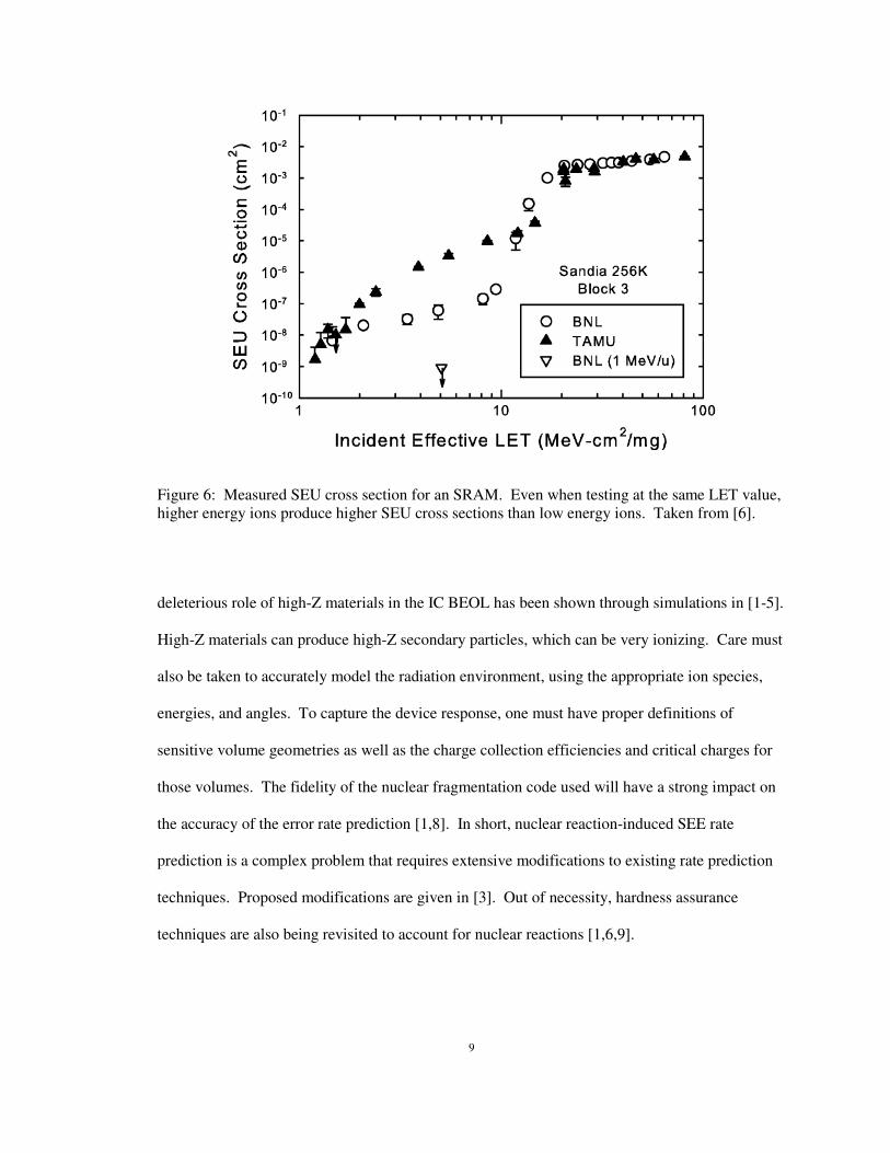
Figure 6: Measured SEU cross section for an SRAM. Even when testing at the same LET value,
higher energy ions produce higher SEU cross sections than low energy ions. Taken from [6]...... 9
Figure 7: Block diagram of a generic pulse height analysis system. This system can be used to
produce a spectrum that characterizes charge generation events in the detector. .......................... 10
Figure 8: Measured pulse height spectrum from 5.4 MeV alpha particles incident on a silicon
surface barrier detector. This spectrum is used to perform an energy calibration by defining the
centroid of the distribution, bin number 495, to occur at 5.4 MeV. ............................................... 11
Figure 9: SOI test structures containing metallization at the (a) W1 and M1 layers, (b) W2 and
M2 layers, and (c) W3 and M3 layers. These and other test structures allow identification of the
role of overlayer materials on charge generation in the active silicon. Not drawn to scale. ......... 15
Figure 10: Block diagram of the 16-channel PHA system and auxiliary equipment. ................... 18
Figure 11: A noise spike on the detector bias supply line caused the anomalous large-amplitude
events shown in (a). These events affect multiple channels in the same digitization cycle, and
were filtered from the data via post-processing, as shown in (b). .................................................. 19
Figure 12: Measurement of the total number of counts during a high fluence heavy ion exposure.
This non-linear curve shows that the count rate was decreasing over time, because of
displacement damage in the diodes. ............................................................................................... 20
Figure 13: LET can be held constant while increasing particle energy by increasing the atomic
number of the ions in the beam. Circles represent the heavy ion beams used in this work.
Generated using SRIM-2008 [15]. ................................................................................................. 22
vi
Figure 14: Measured integral cross section of 40 MeV/u 20
Ne ions on the test structures. The
presence of tungsten near the active silicon led to extreme charge collection events. .................. 23
Figure 15: Measured SEU cross section as a function of energy at an incident effective LET of
~5 MeV·cm2/mg. These data raise the question of whether SEU cross sections increase without
bound as particle energy increases and LET is held constant. Taken from [6]............................. 27
Figure 16: The galactic cosmic ray differential energy spectra for hydrogen, helium, and iron.
Taken from [16]. ............................................................................................................................ 27
Figure 17: Measured integral cross section from the test structures for two heavy ion beams with
the same LET. The higher energy test produced smaller-amplitude charge collection events. .... 28
Figure 18: Measured integral cross section from the test structures for three heavy ion beams
with the same LET. The higher energy test produced smaller-amplitude charge collection events.
....................................................................................................................................................... 28
Figure 19: Simulated integral cross section of various fixed-LET heavy ions on a bulk-Si device.
....................................................................................................................................................... 30
Figure 20: Simulated SEU cross section as a function of energy for a bulk-Si device. The worst-
case energy, or the energy resulting in the highest SEU cross section, depends on Qcrit. .............. 31
Figure 21: Simulated SEU cross section as a function of energy for an SOI device. The worst-
case energy, or the energy resulting in the highest SEU cross section, depends on Qcrit. .............. 32
Figure 22: Simulated nuclear spallation reactions caused by a) 40 MeV/u neon and by
b) 10000 MeV/u iron. These representative events suggest that very high energy nuclear
reactions produce lower-mass and higher-energy secondary particles, which therefore have lower
LET. ............................................................................................................................................... 33
Figure 23: Simulated isobaric cross section for secondary particles resulting from irradiating 184
W with various 1.2 MeV·cm2/mg ions. Results suggest that higher energy incident particles
cause greater decomposition of the target nucleus, producing more intermediate and low mass
secondary particles. ........................................................................................................................ 35
Figure 24: Simulated cross section for the secondary particles produced from various
1.2 MeV·cm2/mg ions incident on 184
W as a function of secondary particle initial LET. Results
suggest that fewer high LET secondary particles are produced when incident particle energy is
increased beyond a certain point. ................................................................................................... 35
Figure 25: Block diagram of the Mesytec MPRS-16 preamplifier/shaping amplifier. The
TRIGGER output (labeled NIM out) cannot be used for this application, because it is produced by
summing the signals from the various channels. ........................................................................... 40
Figure 26: Simplified diagram of the discriminator board with embedded explanations. This
circuit produces a trigger signal that tells the ADC to digitize when the magnitude of a pulse on
any of the 16 channels exceeds Vthreshold. ........................................................................................ 41
1
CHAPTER I
INTRODUCTION
The focus of this thesis is to deepen our understanding of the factors affecting how
nuclear reactions contribute to single event effects (SEEs) in modern integrated circuits (ICs).
Factors studied include overlayer material, overlayer position, and incident particle energy.
Several papers have suggested that the presence of high atomic number (high-Z)
materials, like tungsten, within the IC back end of line (BEOL), leads to extreme charge
generation events through nuclear reactions. These papers rely on nuclear physics simulations [1-
5] and on the analysis of anomalous circuit-level errors [1,3,4,6] to support this claim. In this
work, charge collection measurements [7] were used to directly determine the role of tungsten
overlayers on radiation-induced charge collection. These measurements prove that the presence
of high-Z materials can lead to extreme charge collection events. Furthermore, the data show
that, for the technology studied, the closer tungsten is to the sensitive volume the more efficiently
nuclear reaction-induced charge is collected.
When nuclear reactions dominate the error rate, SEE cross sections have been shown to
increase as particle energy is increased and linear energy transfer (LET) is held constant [1,6]. In
[6], Dodd questioned whether these SEE cross sections would continue to increase as particle
energy is increased to those high energies found in the galactic cosmic ray (GCR) spectrum.
Thus, the ion energy dependence of nuclear reaction-induced SEEs is not well understood. In this
work, heavy ion (atomic mass > 1) tests were performed over the range of 16 MeV/u to
1000 MeV/u at constant LET. The LET was held constant by using heavier ions for the higher
energies. The highest energy data suggest that nuclear reaction-induced charge collection does
not grow without bound as fixed-LET incident particle energy is increased, but rather reaches a
2
maximum at some energy and then decreases. This maximum is the worst-case energy for SEE
susceptibility at that LET, and varies with device layout and technology. A simulation approach
for identifying this worst-case energy is applied to certain bulk-Si and silicon-on-insulator (SOI)
technologies. Nuclear physics simulations are presented, suggesting that the decrease in charge
collection beyond the worst-case energy occurs because the secondary particles produced from
such high-energy nuclear reactions have less mass and higher energy and are therefore less
ionizing than those produced by lower-energy reactions.

3
CHAPTER II
BACKGROUND
Ionization Mechanisms
This section identifies the various mechanisms by which particles having at least one
atomic mass unit can generate electron-hole pairs in a target material. Direct ionization is the
classification for events in which the incident particles themselves generate charge in the target
medium. Indirect ionization occurs when the incident particle produces secondary particles,
which go on to generate charge. There are three types of indirect ionization: inelastic nuclear
reactions, coulomb scattering, and elastic nuclear reactions.
Direct ionization generates electron-hole pairs through the interaction of the positively
charged incident nucleus with the negatively charged electrons in the target material. The metric
used to quantify direct ionization is linear energy transfer (LET). LET is traditionally measured
in units of MeV·cm2/mg. These units arise because the energy transfer per unit path length
(MeV/cm) is normalized by the density of the target material (mg/cm3).
Inelastic nuclear reactions occur when the incident particle strikes a target nucleus,
causing fragmentation and the ejection of secondary particles. A cartoon of such a reaction is
shown in Figure 1. Coulomb scattering—or Rutherford scattering—occurs when the incident
particle gets close enough to the target nucleus that their positive charges cause them to repel
each other through the Coulomb force. If the incident particle gets even closer to the target
nucleus, an elastic nuclear reaction can occur, in which the repulsion between the two particles is
stronger because the nuclear force is stronger than the Coulomb force for ions in close proximity.
Thus, in both elastic nuclear reactions and in coulomb scattering events the final particles have

4
Figure 1: Representation of an inelastic nuclear reaction.
Figure 2: Representation of either a coulomb scattering event, or of an elastic nuclear reaction.
the same mass and atomic numbers as the original particles; only the trajectories and the kinetic
energies of the particles change. These two types of reactions are represented by Figure 2. From
a SEE point of view, inelastic nuclear reactions tend to be the most significant indirect ionization
mechanism, because they tend to have the highest probability of depositing a large amount of
charge in the sensitive regions of an IC. Throughout this thesis, the term nuclear reactions is
used in reference to inelastic nuclear reactions.
5
Nuclear Reaction-Induced Single Event Effects
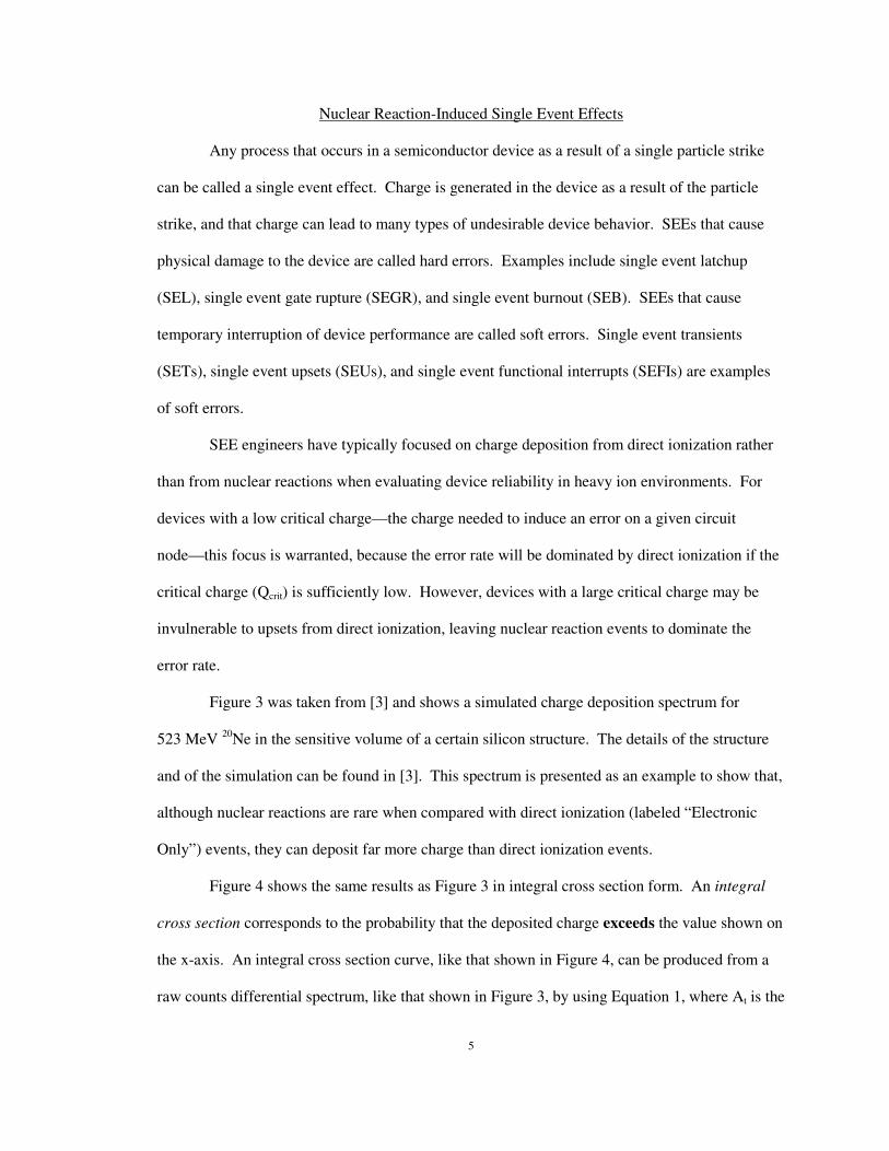
Any process that occurs in a semiconductor device as a result of a single particle strike
can be called a single event effect. Charge is generated in the device as a result of the particle
strike, and that charge can lead to many types of undesirable device behavior. SEEs that cause
physical damage to the device are called hard errors. Examples include single event latchup
(SEL), single event gate rupture (SEGR), and single event burnout (SEB). SEEs that cause
temporary interruption of device performance are called soft errors. Single event transients
(SETs), single event upsets (SEUs), and single event functional interrupts (SEFIs) are examples
of soft errors.
SEE engineers have typically focused on charge deposition from direct ionization rather
than from nuclear reactions when evaluating device reliability in heavy ion environments. For
devices with a low critical charge—the charge needed to induce an error on a given circuit
node—this focus is warranted, because the error rate will be dominated by direct ionization if the
critical charge (Qcrit) is sufficiently low. However, devices with a large critical charge may be
invulnerable to upsets from direct ionization, leaving nuclear reaction events to dominate the
error rate.
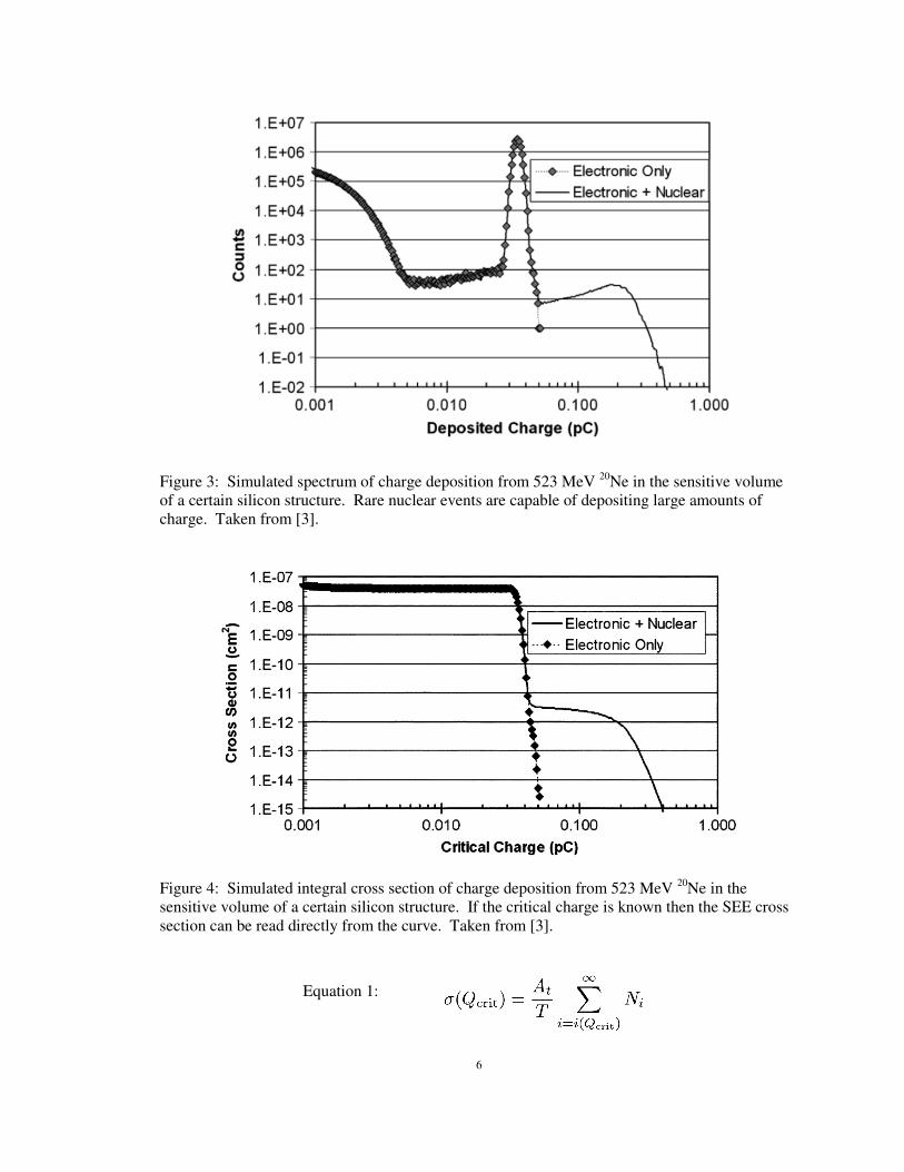
Figure 3 was taken from [3] and shows a simulated charge deposition spectrum for
523 MeV 20
Ne in the sensitive volume of a certain silicon structure. The details of the structure
and of the simulation can be found in [3]. This spectrum is presented as an example to show that,
although nuclear reactions are rare when compared with direct ionization (labeled “Electronic
Only”) events, they can deposit far more charge than direct ionization events.
Figure 4 shows the same results as Figure 3 in integral cross section form. An integral
cross section corresponds to the probability that the deposited charge exceeds the value shown on
the x-axis. An integral cross section curve, like that shown in Figure 4, can be produced from a
raw counts differential spectrum, like that shown in Figure 3, by using Equation 1, where At is the
6
Figure 3: Simulated spectrum of charge deposition from 523 MeV 20
Ne in the sensitive volume
of a certain silicon structure. Rare nuclear events are capable of depositing large amounts of
charge. Taken from [3].
Figure 4: Simulated integral cross section of charge deposition from 523 MeV 20
Ne in the
sensitive volume of a certain silicon structure. If the critical charge is known then the SEE cross
section can be read directly from the curve. Taken from [3].
Equation 1:

7
area of the device, T is the total number of particles that struck the device, and Ni is the number
of events in the ith bin of the raw spectrum [3]. Note that At/T is equivalent to 1/Fluence.
Once an integral cross section is plotted, if the critical charge is known, then the SEE
cross section for that type of error can be read directly from the graph. Thus, if the device in
Figure 4 had a single event upset (SEU) Qcrit of 100 fC then the SEU cross section would be
2 × 10-12
cm2, but if it had a 10 fC Qcrit then the SEU cross section would be 4 × 10
-8 cm
2. Figure 4
also demonstrates that nuclear reactions would dominate the error rate for the higher Qcrit,
whereas direction ionization would dominate the error rate for the lower Qcrit.
Figure 5: Measured SEU cross section for a radiation-hardened SRAM. Nuclear reactions
caused upsets at LET values well below the 40 MeV·cm2/mg SEU LET threshold of the device.
Taken from [3].
Figure 5 [3] shows the measured SEU cross section of a radiation-hardened 4 Mbit
SRAM. The cross section is saturated for very high LET values and drops off sharply below the
LET threshold of 40 MeV·cm2/mg. This portion of the data can be predicted reasonably well
using the conventional rectangular parallelepided (RPP) technique. In this technique, the average
LET of the incident particle is multiplied by the path length of that particle through the sensitive

8
volume to solve for the amount of charge deposited. If this charge exceeds Qcrit then it is
predicted that an upset will occur. However, Figure 5 also shows SEUs at very low LET values.
These upsets cannot be predicted using the RPP model. The author of [3] performed energy
deposition simulations, and was able to predict the cross sections of these upsets reasonably well
when accounting for inelastic nuclear reactions. Therefore, the author of [3] concluded that these
upsets were likely caused by nuclear reactions. Thus, through nuclear reactions, even devices
with a high SEU LET threshold can be upset in a low-LET environment.
Even in devices with a low critical charge, the effects of nuclear reactions can be
significant. Although direct ionization may dominate the single bit upset response of a low-Qcrit
device, nuclear reactions may dominate the multiple bit upset response, the single event
functional interrupt response, the single event latchup response, etc. [1]. In addition, all neutron
induced SEEs, and nearly all proton induced SEEs, occur through nuclear reactions.
Experiments have been performed with various energies of ions having the same LET in
order to attribute observed SEEs to nuclear reactions [1,6]. The premise of these experiments is
that, if direct ionization were the dominant error-inducing mechanism, then ions of the same LET
would produce the same error rate. The results of such an experiment are shown in Figure 6,
which was taken from [6]. The high energy test results in Figure 6, plotted as triangles, show a
much higher cross section for SEUs than the low energy test results, which are plotted as circles.
This disparity suggests that an energy-dependent charge deposition mechanism is responsible for
the observed SEUs. The authors of [1,6] used theory and simulations to attribute these SEUs to
inelastic nuclear reactions.
Because of the complex physics involved, nuclear reaction-induced SEE rate prediction
must be done with high fidelity simulations. It is important to account for the composition and
placement of all materials in or near the sensitive volumes of the device. In particular, the
9
Figure 6: Measured SEU cross section for an SRAM. Even when testing at the same LET value,
higher energy ions produce higher SEU cross sections than low energy ions. Taken from [6].
deleterious role of high-Z materials in the IC BEOL has been shown through simulations in [1-5].
High-Z materials can produce high-Z secondary particles, which can be very ionizing. Care must
also be taken to accurately model the radiation environment, using the appropriate ion species,
energies, and angles. To capture the device response, one must have proper definitions of
sensitive volume geometries as well as the charge collection efficiencies and critical charges for
those volumes. The fidelity of the nuclear fragmentation code used will have a strong impact on
the accuracy of the error rate prediction [1,8]. In short, nuclear reaction-induced SEE rate
prediction is a complex problem that requires extensive modifications to existing rate prediction
techniques. Proposed modifications are given in [3]. Out of necessity, hardness assurance
techniques are also being revisited to account for nuclear reactions [1,6,9].

10
Figure 7: Block diagram of a generic pulse height analysis system. This system can be used to
produce a spectrum that characterizes charge generation events in the detector.
Pulse Height Analysis
All of the charge collection measurements in this work were taken using pulse height
analysis (PHA) [7]. A block diagram describing PHA is given in Figure 7. To perform PHA, a
semiconductor detector is reverse biased in order to ensure that nearly 100% of the charge
generated in the detector will be swept to the contacts by the applied electric field. When
ionizing radiation strikes the detector a current pulse is then induced, and applied to the input of a
charge sensitive preamplifier. The preamplifier integrates current over time; therefore, it outputs
a pulse whose height is a measure of the amount of charge collected from the detector. This pulse
is then amplified and manipulated to have a nearly Gaussian shape by the shaping amplifier. This
shaped pulse is passed to the multichannel analyzer, which digitizes the pulse and histograms it
according to its height. This process is repeated for every event that generates charge in the
detector, and ultimately produces a differential pulse height spectrum.

11
Figure 8: Measured pulse height spectrum from 5.4 MeV alpha particles incident on a silicon
surface barrier detector. This spectrum is used to perform an energy calibration by defining the
centroid of the distribution, bin number 495, to occur at 5.4 MeV.
By calibrating the PHA system, the differential pulse height spectrum can be read directly
in terms of charge collection. Thus, a calibrated PHA system can produce a spectrum like the one
shown in Figure 3. The PHA system used in this work was calibrated using a Polonium-210
radioactive source that emits 5.4 MeV alpha particles. The alpha particles were stopped in a
reverse-biased silicon surface barrier detector (SBD), and therefore deposited their total energy.
Energy deposited in silicon generates charge with a conversion factor of 22.5 keV/fC [10]. Thus,
the amount of charge generation is readily known, and because the SBD has near 100% charge
collection efficiency, this is the amount of charge that is injected into the preamplifier of the PHA
system as a current pulse. These alpha-induced current pulses are processed and digitized to
produce a roughly Gaussian distribution of pulse height events, as shown in Figure 8. The
centroid of this distribution is defined to occur at the energy of the incident alpha particles—
5.4 MeV. This provides one energy calibration point. A second point is obtained by assuming
12
that the 0th bin of the analog-to-digital converter (ADC) corresponds to 0 MeV. Because the PHA
system is highly linear, these two calibration points allow us to interpret all of the 4096 bins of
the ADC in terms of energy deposited. Although this crude calibration method would be
inadequate for some applications (e.g., alpha spectroscopy) it is sufficient for the purposes of this
study.
13
CHAPTER III
EXPERIMENTAL DESIGN
Observability of Nuclear Events
Modern ICs are often composed of millions of devices, and can therefore contain millions
of sensitive volumes. Because of the large number of sensitive volumes, even rare nuclear
reaction events like those shown in Figure 4 can, at times, be readily observed as a deviation from
normal device functionality. One goal of this study is to measure the charge collected from these
rare nuclear reactions events. However, it would be impractical to simultaneously perform PHA
on millions of sensitive devices. The PHA system chosen for this study is capable of
simultaneous charge collection measurements from 16 detectors, allowing for some
parallelization of data acquisition during broadbeam testing. In order to further increase the
observability of nuclear reaction events, the test structures used in this study have a much larger
sensitive volume area than one would find in a realistic IC device. The test structures are
described in the next section.
It was necessary to irradiate the test structures to a minimum fluence of 109 cm
-2 in order
to observe a statistically significant number of rare nuclear events. This high fluence can only be
achieved in a reasonable amount of time by using a high beam flux. There is a limit to the rate at
which a PHA system can process charge collection events. When that rate is exceeded then many
charge deposition events can be missed, because they occur while the PHA system is busy
processing previous events. The percentage of the time that the PHA system is busy is called the
dead time. The dead time was measured and kept low by limiting the flux, and by designing a
high-bandwidth PHA system.

14
Pileup is another testing difficulty that must be considered for when performing PHA on
large area devices with a high beam flux. Pileup occurs when two (or more) incident particles
strike the detector at virtually the same time. The PHA system cannot distinguish these as
separate charge deposition events, so an artificially-high charge collection event is recorded.
Poisson statistics can be used to calculate the probability of an n-fold pileup event, as shown in
Equation 2 [7]. This equation gives the probability for observing exactly n events, when the
expected number of events in the time interval is λ. For the purpose of predicting pileup in a
PHA system, λ can be calculated by multiplying the beam flux by the sensitive area of the
detector and by the shaping time constant used in the shaping amplifier.
Equation 2:
These pileup events can have a higher cross section than nuclear events, and therefore
overwhelm the nuclear events in their respective region of the pulse height spectrum. The
interference of pileup events with the nuclear events being studied was minimized by testing with
low LET ions incident on a relatively thin sensitive volume. These two conditions ensured that
very little charge was generated due to direct ionization, and therefore even when pileup occurs
they affect such low ADC bin numbers that the observability of nuclear events is not reduced.
The lower level discriminator of the PHA system was set in order to cut off these direct ionization
events, which also significantly reduced the system dead time.
High LET beam contaminants were also encountered, and are described in Chapter IV.
These events are similar to pileup in that they can overwhelm the nuclear events in a certain
region of the pulse height spectrum. These events have been identified in the spectra presented in
this work. No effort was made to reduce beam contamination levels because this mechanism was
identified late in the study.

15
Si3N4
SiO2
SiO2M3
SiO2
SiO2
W3
M2
SiO2
AlCu
W2
Ti2Si
W1
Si n+ 1020 cm-3
SiO2 (BOX)
Si (Substrate)
W
SiO2
SiO2
SiO2
SiO2
Ti2Si
SiO2
SiO2
SiO2
SiO2
Ti2Si
W
AlCu
W
AlCu
Si p 1016 cm-3
Si n+ 1020 cm-3
SiO2 (BOX)
Si (Substrate)
Si p 1016 cm-3
Si n+ 1020 cm-3
SiO2 (BOX)
Si (Substrate)
Si p 1016 cm-3
M1
Si3N4
SiO2
Si3N4
SiO2
0.8 µm
3.302 µm
0.87 µm
0.7 µm
675 µm
0.87 µm
0.7 µm
0.87 µm
0.8 µm
0.04 µm
0.08 µm
0.13 µm
0.2 µm
a) b) c)
Figure 9: SOI test structures containing metallization at the (a) W1 and M1 layers, (b) W2 and
M2 layers, and (c) W3 and M3 layers. These and other test structures allow identification of the
role of overlayer materials on charge generation in the active silicon. Not drawn to scale.
Test Structures
Sandia National Laboratories fabricated SOI vertical n+/p diodes for this study with their
CMOS7 technology. The diodes have a large surface area, 307 × 601 µm2, in order to maximize
the number of events that can be observed during a reasonable heavy ion exposure. They were
overlaid with various materials in order to determine the overlayers’ effect on charge collection in
the diode. In this paper, the metallization layers are identified with either a “W”, for tungsten
layers, or with an “M”, for the AlCu metal layers, followed by the level number (e.g., W1 is
tungsten level 1, meaning the level closest to the silicon).
Several overlayer configurations were fabricated, three of which are shown in Figure 9.
The “W1 + M1” configuration is shown in Figure 9(a). Looking up from the charge collection
region (i.e., the silicon body) it contains a thin sheet of titanium silicide, 75% tungsten coverage
in the W1 layer, a sheet of AlCu at the M1 layer (actual composition, from bottom to top: Ti
0.02 µm /TiN 0.05 µm /AlCu 0.7 µm /TiN 0.1 µm), and 100% oxide on all other process
metallization layers. Figure 9(b) shows the “W2 + M2” configuration, which is the same
structure except that the W and AlCu are one level higher. These materials are raised an

16
additional level in the “W3 + M3” configuration, shown in Figure 9(c). The “M1” structure (not
shown) only has AlCu at level 1. The final structure used in this study (not shown in figure) is
called “Oxide Only”. It contains no W or AlCu.
These test structures allow us to isolate and identify the contributions of the W and AlCu
layers to charge collection in the underlying silicon body. Note that 75% W coverage and 100%
AlCu coverage is far more metallization than is used in typical IC devices. This was done to
make the effects of the metallization on charge collection more observable. For all tests the
diodes were reverse biased with 3 V and the substrate was grounded.
The diodes were fabricated in a SOI technology with the intent of having well-defined
sensitive volumes. One must have clearly defined sensitive volumes to be able to quantitatively
compare experimental data with energy deposition simulation results. With SOI devices,
typically charge is collected only from the silicon body; the buried oxide prevents any charge
from being collected from the substrate. However, high LET heavy ion tests (ranging from 10 –
60 MeV·cm2/mg) revealed that the sensitive volume thickness of these diodes extends as deep as
several microns into the substrate. Testing further revealed that the sensitive volume thickness of
the diodes is not constant for various LET values, although charge collection does increase
monotonically as LET is increased. Finally, testing revealed that coincident charge collection
events often occur in separate diodes, but only for diodes located on the same die. These
complex charge collection mechanisms in the diodes were identified as being caused by
displacement currents. These test structures are very similar to those used in [11,12] for studying
displacement currents in that they have a large area, low substrate doping, and a relatively thin
buried oxide (200 nm). Unfortunately, these are also the conditions under which displacement
current becomes significant. This complex charge collection mechanism occurs because the
electric field from the reverse biased diode in the silicon body penetrates some distance into the
substrate. This electric field separates the charges that are generated in the substrate, and causes

17
charge of a certain polarity to accumulate beneath the buried oxide. This charge is mirrored in
the silicon body because the silicon body and the substrate act as the plates of a capacitor. This
charge is then collected by the PHA system. In [11,12] it was shown that this mechanism could
cause charge sharing between devices separated by hundreds of microns of SiO2, as was the case
here. Despite this complex charge collection mechanism, data from these test structures are still
useful because they can be used to show differences in charge collection between diodes having
different overlayer configurations. However, this mechanism prevents us from being able to
quantitatively compare experimental data with energy deposition simulation results.
Test Setup
A block diagram of the test configuration is given in Figure 10. The 16-channel PHA
system designed for this study relies on the Mesytec MPRS-16 preamplifier/shaping amplifier,
used in conjunction with the Phillips Scientific 7164H peak sensing ADC. The 7164H is a
module following the Computer Automated Measurement And Control (CAMAC) standard, so a
CAMAC crate controller is needed to interface with it. The Kinetic Systems 3988 General
Purpose Interface Bus (GPIB) crate controller was used. In order to prevent the long latency of
the GPIB standard from reducing the PHA system’s bandwidth, a HYTEC 1342 auxiliary crate
controller was used in List Mode. The 1342 stored the PHA events in a buffer, which was
periodically read out by the 3988. The software controlling it all was written by Marcus
Mendenhall using the Python Laboratory Operations Toolkit [13]. This software saves every
digitization event with a timestamp, allowing for great flexibility when postprocessing data.
A discriminator board was designed and built as a custom printed circuit board (PCB), in
order to detect when a shaped pulse from the Mesytec exceeded some threshold voltage, and then
to trigger the Phillips Scientific 7164H to digitize that pulse. The design of the discriminator

18
Da
ta R
oo
mTa
rge
t R
oo
m
NIM bin and power supply
(Ortec 4001A/4002A)
Pulse
generator
(Ortec 480)
CAMAC crate and power supply
(Kinetic Systems 1502)
MCA
(Phillips
Scientific
7164H)
Counter
(Kinetic
Systems
3615)
Auxiliary
Crate
controller
(Hytec 1342)
GPIB Crate
controller
(Kinetic
Systems 3988)
Heavy ion beam
Board containing
devices under
test (SOI diodes)
Preamplifier/Shaping
Amplifier
(Mesytec MPRS-16)
Detector bias
supply
(Keithley 2410)
Ethernet/GPIB
Gateway
(Agilent E5810A)
Discriminator board
/ Dead-time board
(custom built PCB)
Power supply
(HP E3631A)
Vthreshold
Inp
ut
x16
GA
TE
Oscilloscope
(Tektronix
TDS 340A)
Router
Ethernet/GPIB
Gateway
(Agilent E5810A)
Laptop
computer for
data
acquisition
Figure 10: Block diagram of the 16-channel PHA system and auxiliary equipment.
board is given in Appendix A. Note that, once triggered, the 7164H digitizes the signals present
at that moment on all 16 inputs. This increases the dead time of the PHA system. However, it
also allowed for the identification of anomalous events that were manifest as large-amplitude

19
charge collection events affecting multiple channels at the same time. One such type of
anomalous event is shown in Figure 11(a). These events were identified as being caused by noise
spikes on the detector bias supply power line (see Figure 7). These events were removed from
the pulse height spectra through postprocessing, as is shown in Figure 11(b). As mentioned in the
Test Structures section, another such type of anomalous event was identified as being caused by
displacement currents in the test structures, which caused charge sharing between diodes on the
same die. These coincident events were also removed through postprocessing.
a) b)
Figure 11: A noise spike on the detector bias supply line caused the anomalous large-amplitude
events shown in (a). These events affect multiple channels in the same digitization cycle, and
were filtered from the data via post-processing, as shown in (b).
The dead time of the system was measured by sampling the BUSY signal of the 7164H at
10 MHz. The fraction of the time that BUSY was asserted was defined as the dead time, and was
determined using the Kinetic Systems 3615 Counter.
Displacement damage in the diodes was observed following certain high-fluence heavy
ion tests, particularly when testing with lower energy incident particles. This damage causes a

20
Figure 12: Measurement of the total number of counts during a high fluence heavy ion exposure.
This non-linear curve shows that the count rate was decreasing over time, because of
displacement damage in the diodes.
decrease in the charge collection efficiency of the diodes; therefore, its occurrence must be
identified so that the damaged diodes can be replaced with new ones. The proper functionality of
the diodes was monitored by continuously measuring the leakage currents of the diodes by using
a Keithley 2410 as the detector bias supply. Displacement damage in the diode is accompanied
by a significant increase in leakage current. Displacement damage was also detected by
observing that the count rate of the PHA system steadily decreased, even though the beam flux
was constant. Figure 12 shows how the total number of counts increased while the diodes were
irradiated with 10 MeV/u oxygen to a fluence of 2 × 10¹⁰
cm-2
. If the count rate were constant
over time then Figure 12 would show a straight line. Instead, the count rate is seen to steadily
decrease, due to the reduced charge collection efficiency of the damaged diodes.
An oscilloscope was used throughout the experiments to view the unipolar pulses that
were being digitized. An oscilloscope is useful to identify noise sources so that they can be
21
eliminated, and so that the experimenter will know if the unipolar pulses being digitized are ill-
formed or saturated.
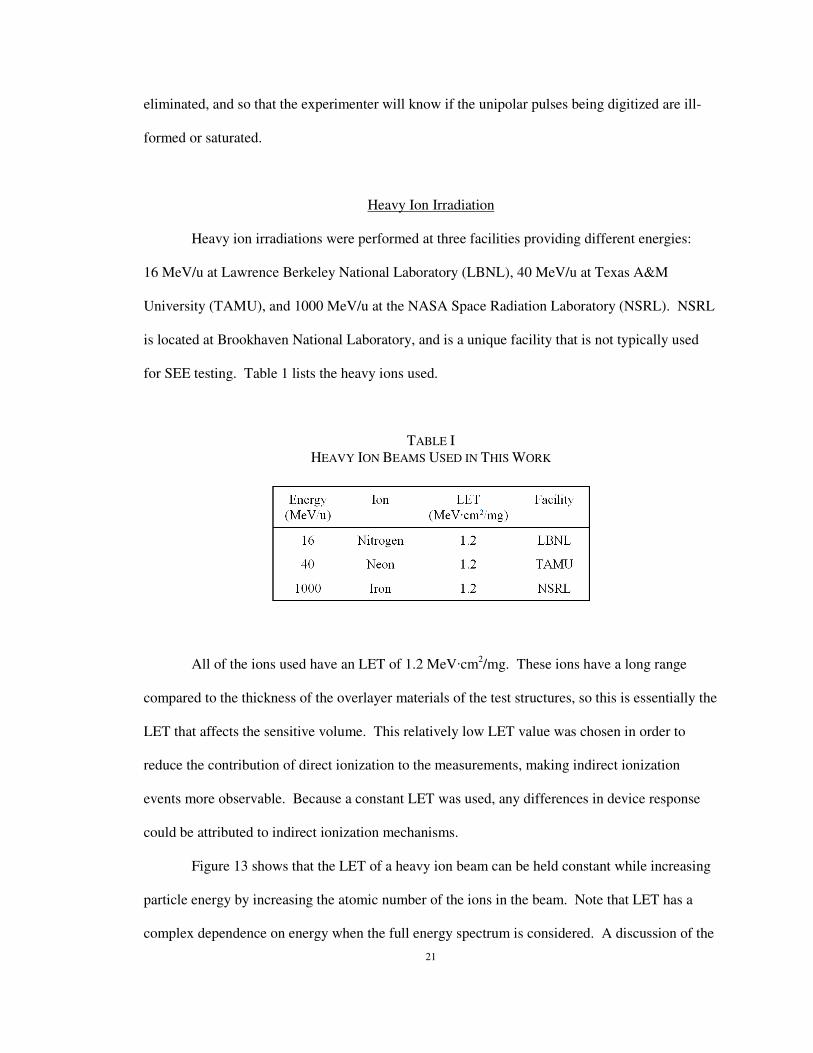
Heavy Ion Irradiation
Heavy ion irradiations were performed at three facilities providing different energies:
16 MeV/u at Lawrence Berkeley National Laboratory (LBNL), 40 MeV/u at Texas A&M
University (TAMU), and 1000 MeV/u at the NASA Space Radiation Laboratory (NSRL). NSRL
is located at Brookhaven National Laboratory, and is a unique facility that is not typically used
for SEE testing. Table 1 lists the heavy ions used.
TABLE I
HEAVY ION BEAMS USED IN THIS WORK
All of the ions used have an LET of 1.2 MeV·cm2/mg. These ions have a long range
compared to the thickness of the overlayer materials of the test structures, so this is essentially the
LET that affects the sensitive volume. This relatively low LET value was chosen in order to
reduce the contribution of direct ionization to the measurements, making indirect ionization
events more observable. Because a constant LET was used, any differences in device response
could be attributed to indirect ionization mechanisms.
Figure 13 shows that the LET of a heavy ion beam can be held constant while increasing
particle energy by increasing the atomic number of the ions in the beam. Note that LET has a
complex dependence on energy when the full energy spectrum is considered. A discussion of the

22
Figure 13: LET can be held constant while increasing particle energy by increasing the atomic
number of the ions in the beam. Circles represent the heavy ion beams used in this work.
Generated using SRIM-2008 [15].
physics of energy loss can be found in [14]. SEE testing is typically performed at energies
between a few MeV/u and 1000 MeV/u. Within this energy range, the same LET can be obtained
using a variety of ions at the appropriate energies.
23
CHAPTER IV
IMPACT OF THE PRESENCE AND PLACEMENT OF TUNGSTEN
The results of 40 MeV/u 20
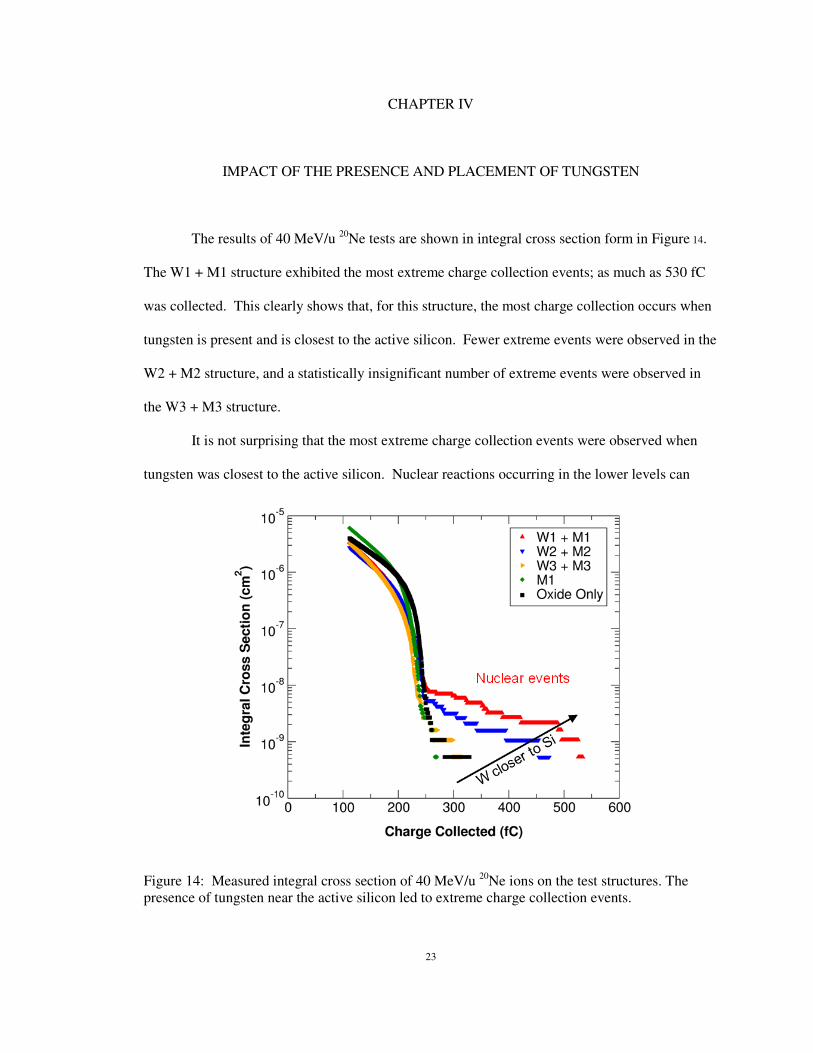
Ne tests are shown in integral cross section form in Figure 14.
The W1 + M1 structure exhibited the most extreme charge collection events; as much as 530 fC
was collected. This clearly shows that, for this structure, the most charge collection occurs when
tungsten is present and is closest to the active silicon. Fewer extreme events were observed in the
W2 + M2 structure, and a statistically insignificant number of extreme events were observed in
the W3 + M3 structure.
It is not surprising that the most extreme charge collection events were observed when
tungsten was closest to the active silicon. Nuclear reactions occurring in the lower levels can
Figure 14: Measured integral cross section of 40 MeV/u 20
Ne ions on the test structures. The
presence of tungsten near the active silicon led to extreme charge collection events.

24
more easily eject secondary particles at high angles through the sensitive volume, allowing them
to deposit more charge due to their longer path length. Also, secondary particles originating at
higher levels may have insufficient range to reach the sensitive volume. Finally, secondary
particles originating at higher levels lose energy as they penetrate the lower levels. If a secondary
particle has an initial energy corresponding to the Bragg peak energy for that ion (see the function
maxima in Figure 13) then the loss of energy in overlayers would make the particle less ionizing.
However, if its initial energy is greater than the Bragg peak energy, it can be seen in Figure 13
that the loss of energy in overlayers could make the particle more ionizing. Therefore, under
certain conditions, it is possible that tungsten further from the sensitive volume could contribute
the most to nuclear reaction-induced charge generation.
These findings somewhat differ from those given in [5], in which simulation results for a
certain device showed little charge generation dependence on the vertical position of the tungsten
plugs, but a strong dependence on the lateral position of the tungsten plugs relative to the
sensitive volume. However, the structure simulated in [5] had a smaller sensitive volume that
was laterally offset from the overlying tungsten plugs (corresponding to the layout of an actual
SRAM cell), and, as the author noted, the angular distribution of the secondary particles affected
the outcome of the study. Therefore, when considered together, Figure 14 and the work of [5]
strongly suggest that nuclear reaction-induced charge generation is a function of the vertical and
lateral position of the tungsten relative to the sensitive volume, as well as the nuclear breakup
pattern.
No statistical difference can be seen between the responses of the M1 and Oxide Only
structures in Figure 14, meaning the Ti/TiN/AlCu/TiN metal layer did not cause any more large-
amplitude events than similarly placed SiO2 layers. This meets expectations because the fraction
of the M1 layer filled by Ti or Cu is too small to significantly affect the cross sections, and the
lower-Z Al and N atoms will have the same effect as oxide because they can only produce low-Z

25
secondary particles, which therefore have low LET. These results show that high-Z materials
have a greater impact on nuclear reaction-induced charge collection than low-Z materials.
No events are shown in Figure 14 below 120 fC because that is where the discriminator
was set during heavy ion irradiation. This was done to keep the count rate low so that dead time
losses in the PHA system would not reduce the observability of extreme charge collection events.
Direct ionization events caused by 40 MeV/u 20
Ne are not shown because they fall beneath this
threshold, however they have an integral cross section value of 1.8 × 10⁻³
cm2 (the diode area).
The events below 250 fC are likely caused by direct ionization from beam contaminants (i.e., ions
in the beam other than 20
Ne). Because of this finding it is recommended that studies focused on
low cross section events (e.g., nuclear reactions) should first characterize the beam’s purity, and,
when possible, purge high-LET contaminants from the beam. The events beyond 250 fC are
clearly caused by nuclear reactions because their cross sections are several orders of magnitude
below the 20
Ne direct ionization events. Despite their rarity, these extreme charge collection
events can dominate the error rate in devices with a high critical charge [1-3].

26
CHAPTER V
IMPACT OF ION ENERGY ON CHARGE COLLECTION
Data on Ion Energy Dependence
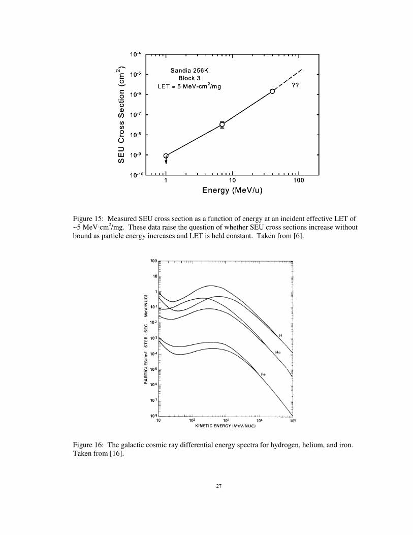
Figure 15 was taken from [6], and shows that SEU cross sections for the SRAM studied
increase as incident particle energy increases and LET is held constant. However, data are only
given up to 40 MeV/u, and the author questioned whether these SEU cross sections increase
without bound as primary particle energy increases [6]. Such an increasing trend could lead to
the vast underprediction of on-orbit error rates, because heavy ions exist in the space environment
that are far more energetic than those typically used in ground facilities for hardness assurance
testing. Figure 16 was taken from [16], and shows the differential energy spectra of a few
prominent ions in the GCR spectrum. As seen in Figure 16, the differential flux peak of GCR
ions is approximately 500 MeV/u. However, the median differential flux is approximately
1500 MeV/u, so half of all the ions in the GCR spectrum have energies exceeding this value.
Thus, GCR energies are orders of magnitude greater than those used for ground based testing, so
it is vitally important to understand the effect of ion energy on nuclear reaction induced SEEs.
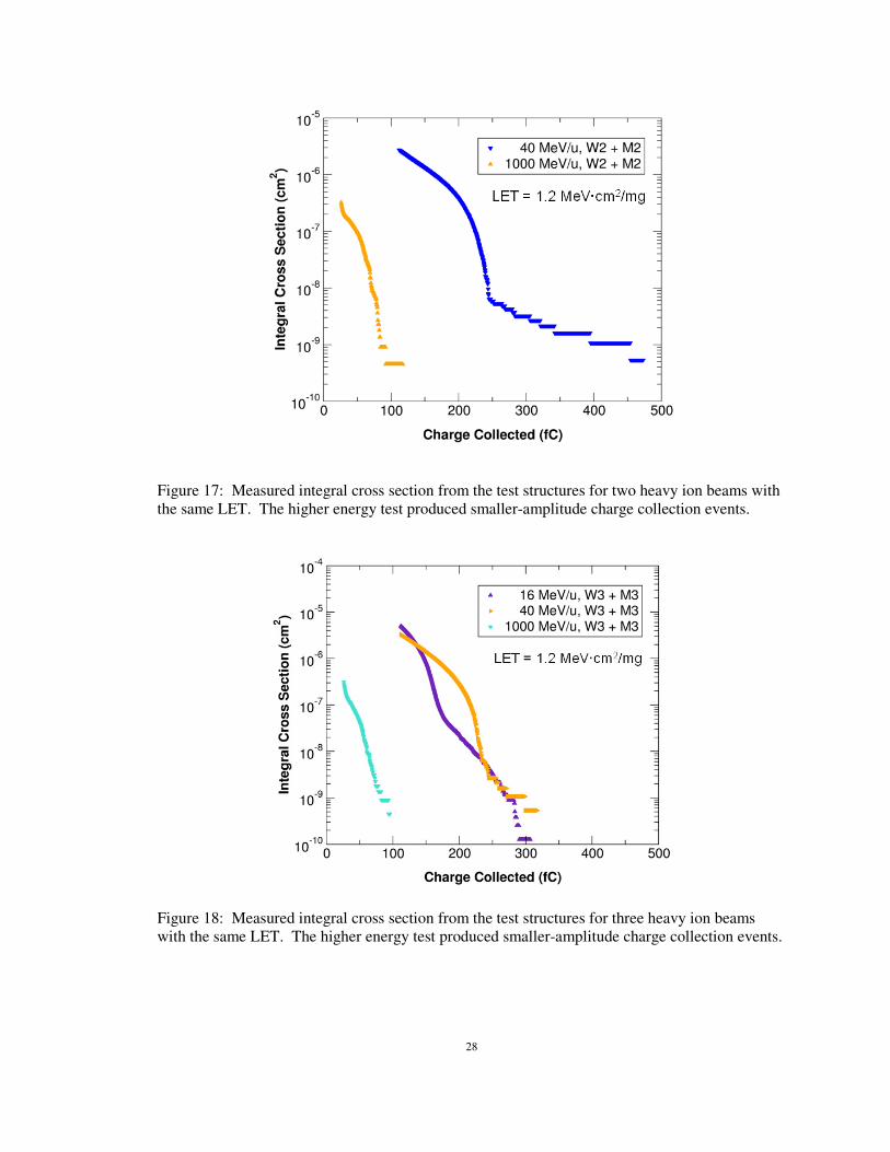
Tests were performed at NSRL with 1000 MeV/u 56
Fe—a prominent and potentially very
harmful ion in the GCR spectrum. This ion has the same LET as 40 MeV/u 20
Ne:
1.2 MeV⋅cm2/mg. Although 1000 MeV/u
56Fe is a more energetic and heavier ion than 40 MeV/u
20Ne, Figure 17 shows that 40 MeV/u
20Ne resulted in larger-amplitude charge collection events.
With 1000 MeV/u 56
Fe, events in the W2 + M2 structure were limited to 115 fC, whereas with
40 MeV/u 20
Ne they ranged up to 470 fC. This clearly shows that nuclear reaction-induced
27
Figure 15: Measured SEU cross section as a function of energy at an incident effective LET of
~5 MeV·cm2/mg. These data raise the question of whether SEU cross sections increase without
bound as particle energy increases and LET is held constant. Taken from [6].
Figure 16: The galactic cosmic ray differential energy spectra for hydrogen, helium, and iron.
Taken from [16].
28
Figure 17: Measured integral cross section from the test structures for two heavy ion beams with
the same LET. The higher energy test produced smaller-amplitude charge collection events.
Figure 18: Measured integral cross section from the test structures for three heavy ion beams
with the same LET. The higher energy test produced smaller-amplitude charge collection events.

29
charge collection does not grow without bound as particle energy increases and LET is held
constant, and suggests that, beyond a certain energy, it actually decreases. This turning-point
energy is therefore the worst-case energy for SEE testing at that LET, and depends on the device
layout and technology. The mechanism responsible for the decrease in nuclear reaction-induced
charge collection beyond the worst-case energy is explored in the Physical Mechanism section.
Figure 18 shows the integral cross section of heavy ion data on the W3 + M3 test
structures at 16 MeV/u, 40 MeV/u, and 1000 MeV/u, all with the same LET. These data are
consistent with Figure 15 because 40 MeV/u resulted in a similar response as 16 MeV/u. They
are also consistent with Figure 17 because 1000 MeV/u is again seen to result in lower-amplitude
charge collection events. This suggests that the worst-case energy for nuclear reaction-induced
charge collection exists somewhere between 40 MeV/u and 1000 MeV/u at this LET for these
devices.
Simulations Identifying Worst-Case Energy
Previous simulation results for a bulk-Si device showed the impact of 25 MeV/u and
500 MeV/u heavy ions on indirect ionization [2]. These results showed that when tungsten was
present in the device, higher-energy testing was needed to produce a conservative estimate of the
on-orbit response. However, [2] does not identify the high energy that should be used for SEE
testing. In order to identify the worst-case energy for nuclear reaction-induced charge generation,
simulations were performed using Monte Carlo Radiative Energy Deposition (MRED) [1-3,5], a
Geant4-based radiation transport code developed at Vanderbilt University. MRED version 9.0.0
was used—which relies on Geant4 9.2.p01—with the binary cascade nuclear fragmentation
model. MRED was also used to guide the experiments and to provide insight into nuclear
interaction mechanisms.

30
The worst-case energy for nuclear reaction-induced charge generation will depend on the
technology, the device layout, and the fixed LET value chosen. The following examples
demonstrate the approach to identify the worst-case energies of certain bulk-Si and SOI devices.
The bulk-Si SEU hardened SRAM presented in [3] was simulated in this work. As was
done in [3], the metallization was simplified in the simulations as a sheet of tungsten at level 2
and sheets of aluminum at levels 1-3. The sensitive volume is 2 × 2 µm2 laterally and 2.25 µm
thick. This sensitive volume was placed at the top center of a 50 × 50 × 50 µm3 substrate so that
the simulation would account for secondary particles originating far away from the sensitive
volume. MRED was then used to simulate irradiations of the device at normal incidence with
various ion energies and species, all having an LET of 1.2 MeV·cm2/mg. Note that
56Fe has this
same LET at 10000 MeV/u and at 1000 MeV/u, as seen in Figure 13. The resulting integral cross
section curves of five of the energies simulated are shown in Figure 19.
Figure 19: Simulated integral cross section of various fixed-LET heavy ions on a bulk-Si device.

31
Figure 20: Simulated SEU cross section as a function of energy for a bulk-Si device. The worst-
case energy, or the energy resulting in the highest SEU cross section, depends on Qcrit.
As seen in Figure 19, if the critical charge to cause an upset is greater than the charge
deposited by direct ionization events, then nuclear reaction events will dominate the error rate.
The worst-case energy (i.e., the energy producing the highest integral cross section) will depend
on the critical charge. In [3], the SEU hardened SRAM cell had a Qcrit of 1200 fC. This critical
charge was then applied to the integral cross section curves, producing the set in Figure 20
labeled “1200 fC Qcrit”. Figure 20 shows the simulated SEU cross sections as a function of ion
energy for 1.2 MeV·cm2/mg ions. It can be seen that the worst-case energy for this 1200 fC
critical charge device is approximately 100 MeV/u, and that beyond this energy the SEU cross
sections decrease. However, if the device had a 200 fC critical charge then the Figure 20 set
labeled “200 fC Qcrit” would show its SEU energy dependence. This set shows very little
dependence on ion energy, and testing at 16 MeV/u would produce a conservative estimate of the
on-orbit response for this LET.
Corresponding simulations were performed on the CMOS7 Sandia SOI technology tested
in this paper. A sheet of tungsten was again simulated at level 2, and the sensitive volume

32
Figure 21: Simulated SEU cross section as a function of energy for an SOI device. The worst-
case energy, or the energy resulting in the highest SEU cross section, depends on Qcrit.
dimensions used were 2 × 2 µm2 laterally and 0.13 µm thick. By producing the integral cross
section curves and again choosing a critical charge of 200 fC, the Figure 21 set labeled “200 fC
Qcrit” was produced. This shows that such a device would have a worst-case energy of about
500 MeV/u for this LET. The worst-case energy is higher for the SOI device than for the bulk-Si
device, primarily because the interaction of secondary particles with the SOI device’s thinner
sensitive volume leads to a different charge deposition response. If the SOI device had a 20 fC
critical charge, then the Figure 21 set labeled “20 fC Qcrit” would show its SEU energy
dependence. As seen in the bulk-Si device, this low Qcrit value results in a weak SEU dependence
on ion energy, and testing at lower energies would sufficiently estimate the on-orbit response.
These results show that the worst-case energy depends not only on the materials surrounding the
device, but also on the critical charge and the dimensions of the sensitive volume.
33
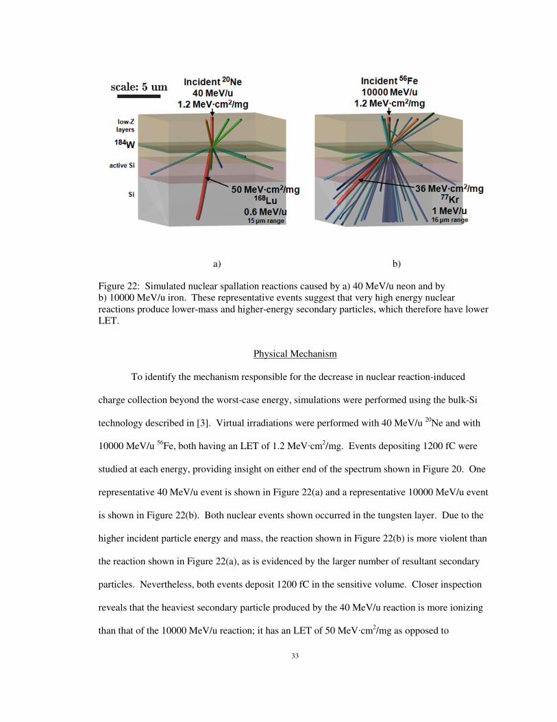
a) b)
Figure 22: Simulated nuclear spallation reactions caused by a) 40 MeV/u neon and by
b) 10000 MeV/u iron. These representative events suggest that very high energy nuclear
reactions produce lower-mass and higher-energy secondary particles, which therefore have lower
LET.
Physical Mechanism
To identify the mechanism responsible for the decrease in nuclear reaction-induced
charge collection beyond the worst-case energy, simulations were performed using the bulk-Si
technology described in [3]. Virtual irradiations were performed with 40 MeV/u 20
Ne and with
10000 MeV/u 56
Fe, both having an LET of 1.2 MeV·cm2/mg. Events depositing 1200 fC were
studied at each energy, providing insight on either end of the spectrum shown in Figure 20. One
representative 40 MeV/u event is shown in Figure 22(a) and a representative 10000 MeV/u event
is shown in Figure 22(b). Both nuclear events shown occurred in the tungsten layer. Due to the
higher incident particle energy and mass, the reaction shown in Figure 22(b) is more violent than
the reaction shown in Figure 22(a), as is evidenced by the larger number of resultant secondary
particles. Nevertheless, both events deposit 1200 fC in the sensitive volume. Closer inspection
reveals that the heaviest secondary particle produced by the 40 MeV/u reaction is more ionizing
than that of the 10000 MeV/u reaction; it has an LET of 50 MeV·cm2/mg as opposed to

34
36 MeV·cm2/mg. It is more ionizing because it has a mass of 168 as opposed to 77. These events
suggest that secondary particles produced from very high energy nuclear reactions tend to have
lower mass and higher energy than those produced by lower-energy reactions, and are therefore
less ionizing. This fragmentation trend could explain the measurements in Figures 17 and 18 in
which charge collection decreased at higher particle energies, and in Figures 20 and 21 in which
simulated SEU cross sections decreased at higher particle energies.
Of course, it would be inappropriate to form any conclusion based on only two nuclear
reaction events. Monte Carlo simulations are needed to understand the statistical nature of
nuclear fragmentation patterns. Such simulations were performed to test the theory that very high
energy incident particles lead to greater decomposition of the incident and target nuclei, resulting
in lower mass and higher energy secondary particles that are less ionizing.
Figure 23 shows the simulated isobaric cross section for secondary particles resulting
from irradiating 184
W with various 1.2 MeV·cm2/mg ions. This shows the mass distribution of
secondary particles for these projectile-target ion pairs. The cross section is given in units of
millibarns. One millibarn is equal to 10-27
cm2. The reason the cross section is so low is that the
raw number reported by the simulator has been divided not only by the fluence (as is normally
done), but also by the number of W atoms in the target material. Thus, the isobaric cross section
is proportional to the probability that an incident particle reacts with a single atom of the target
material to produce a secondary particle of a given mass.
The 40 MeV/u 20
Ne curve in Figure 23 exhibits a peak just below the full mass of the
184W target, which results from reactions in which a few small fragments are removed. This
curve also exhibits peak at roughly half the target mass, resulting from fission of the excited W
nucleus which most likely arises from very peripheral collisions. The higher energy curves
exhibit a broad distribution of secondary masses, because the collisions are sufficiently energetic
to remove a large number of fragments from the target nucleus. This supports the theory that

35
Figure 23: Simulated isobaric cross section for secondary particles resulting from irradiating 184
W with various 1.2 MeV·cm2/mg ions. Results suggest that higher energy incident particles
cause greater decomposition of the target nucleus, producing more intermediate and low mass
secondary particles.
Figure 24: Simulated cross section for the secondary particles produced from various
1.2 MeV·cm2/mg ions incident on 184
W as a function of secondary particle initial LET. Results
suggest that fewer high LET secondary particles are produced when incident particle energy is
increased beyond a certain point.
36
higher energy incident particles lead to greater decomposition of the target nucleus, resulting in
more intermediate and low mass secondary particles. The two higher energy curves are similar
because, in both cases, the energy available is far greater than the binding energy of the target
nucleus, and because the incident 52
Cr and 56
Fe ions have similar mass.
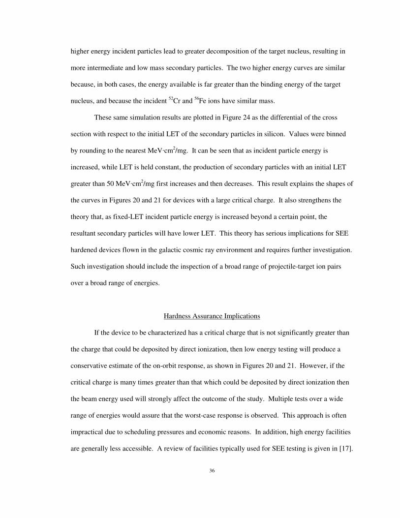
These same simulation results are plotted in Figure 24 as the differential of the cross
section with respect to the initial LET of the secondary particles in silicon. Values were binned
by rounding to the nearest MeV·cm2/mg. It can be seen that as incident particle energy is
increased, while LET is held constant, the production of secondary particles with an initial LET
greater than 50 MeV·cm2/mg first increases and then decreases. This result explains the shapes of
the curves in Figures 20 and 21 for devices with a large critical charge. It also strengthens the
theory that, as fixed-LET incident particle energy is increased beyond a certain point, the
resultant secondary particles will have lower LET. This theory has serious implications for SEE
hardened devices flown in the galactic cosmic ray environment and requires further investigation.
Such investigation should include the inspection of a broad range of projectile-target ion pairs
over a broad range of energies.
Hardness Assurance Implications
If the device to be characterized has a critical charge that is not significantly greater than
the charge that could be deposited by direct ionization, then low energy testing will produce a
conservative estimate of the on-orbit response, as shown in Figures 20 and 21. However, if the
critical charge is many times greater than that which could be deposited by direct ionization then
the beam energy used will strongly affect the outcome of the study. Multiple tests over a wide
range of energies would assure that the worst-case response is observed. This approach is often
impractical due to scheduling pressures and economic reasons. In addition, high energy facilities
are generally less accessible. A review of facilities typically used for SEE testing is given in [17].

37
As an alternative to testing at various energies, the energy producing the worst-case
response can be identified through simulations following the approach described in this chapter.
The accuracy of this method will depend on the fidelity of the nuclear fragmentation models used.
The validation and improvement of these models for SEE rate prediction applications is an
ongoing area of research [1,8]. Further information on the implications of nuclear reactions on
hardness assurance can be found in [1,6,9].

38
CHAPTER VI
CONCLUSIONS
Direct charge collection measurements from test structures overlaid with various BEOL
materials prove that the presence of high-Z materials (e.g., tungsten) leads to extreme charge
collection events through nuclear reactions. For the devices and radiation environments studied,
the data show that tungsten nearest the sensitive volume leads to the most extreme charge
collection events; however, this finding may not be universally applicable. (E.g., it is conceivable
that tungsten further from the sensitive volume could contribute the most to charge collection, if
its position caused enough secondary particles to reach their Bragg peaks in the sensitive
volume.)
For a fixed incident particle LET, increasing the energy beyond a certain point
causes a decrease in nuclear reaction-induced charge collection. This suggests that a worst-case
energy exists for SEE susceptibility, which depends on the technology, device layout, critical
charge, and the incident ions’ fixed LET value. A Monte Carlo simulation approach to determine
the worst-case energy has been applied to example bulk-Si and SOI technologies. Nuclear
fragmentation simulations suggest that the decrease in charge collection beyond the worst-case
energy occurs because the secondary particles produced from very high energy nuclear reactions
tend to have lower mass and higher energy than those produced by lower-energy reactions, and
are therefore less ionizing.

39
APPENDIX
DISCRIMINATOR BOARD DESIGN
The Mesytec MPRS-16 preamplifier/shaping amplifier provides a TRIGGER output
signal that is typically used to trigger the multichannel analyzer. However, it can be seen in
Figure 25 that the TRIGGER is implemented in hardware by summing the signals from the
various channels, in groups of four. The sum of the four channels is then fed into a discriminator,
and if the pulse exceeds the discriminator limit then TRIGGER is asserted. This implementation
assumes that the signals on the separate channels were caused by the same radiation event and are
coincident in time. The MPRS-16 is built this way because it is typically used by nuclear
physicists to perform PHA on various detectors that are affected by a single radiation event (e.g.,
detecting each of the secondary particles from a single nuclear spallation reaction in a gold foil).
In this situation, it makes sense to discriminate the sum of multiple signals, because the sum of
those signals describes the charge deposited by the same radiation event.
In this work, the MPRS-16 is used to perform PHA on 16 detectors in order to increase
the observability of nuclear reactions, and the pulses from these separate detectors are not
coincident in time because they are caused by separate radiation events. Therefore, it would be
inappropriate to perform discrimination on the sum of these signals. The MPRS-16’s TRIGGER
signal could not be used because it was observed that noise on four channels summed together to
exceed the MPRS-16’s discriminator setting, so that TRIGGER was frequently asserted when it
should not have been.
In order to perform discrimination on each of the 16 channels individually it was
necessary to design and build a custom PCB. A simplified diagram of the custom discriminator
board is given in Figure 26.

40
Figure 25: Block diagram of the Mesytec MPRS-16 preamplifier/shaping amplifier. The
TRIGGER output (labeled NIM out) cannot be used for this application, because it is produced by
summing the signals from the various channels.

41
Input (2 x 17 pin header connector)
Injects unipolar pulses from MPRS-
16 output. 16 differential signals
for 16 channels
To channels 1-15
(buffers, comparators)
Unity gain buffer amplifier with
differential inputs. Excellent
common-mode rejection ratio for
noise rejection.
channel 0
Comparator output set to “0”
when magnitude of buffered
pulse exceeds Vthreshold
Vthreshold input, common
to all 16 channels’
comparators.
To input of Phillips
Scientific 7164H Peak-
sensing ADC
Buffer(Analog
Devices
AMP03)
Comparator(LM311)
+ 5 V
Pull-up resistor
10 kΩ
Wire-Ored to
outputs of three
other comparators
4-input
AND gate
(74LS21)
Each input connected
to the wire-ORed
combination of 4
comparator outputs
→ all 16 channels’
comparator outputs
ANDed together
→ AND output = ‘0’ if
any comparator
output = ‘0’
One-shot
timer #1
(74123)
One-shot
timer #2
(74123)
First one-shot produces 8 µs pulse.
Second one-shot produces 2 µs pulse.
This 2 µs pulse defines a 2 µs window
over which the ADC will digitize. After
this 2 µs window, digitization is inhibited
for 6 µs (because of the first one-shot)
→ spurious oscillations won’t be
digitized as if they were valid pulses.
TTL-ECL Logic
converter
(MC10ELT24-D)
To GATE input of
Phillips Scientific
7164H Peak-sensing
ADC (ECL logic).
Figure 26: Simplified diagram of the discriminator board with embedded explanations. This
circuit produces a trigger signal that tells the ADC to digitize when the magnitude of a pulse on
any of the 16 channels exceeds Vthreshold.

42
REFERENCES
[1] R. A. Reed, R. A. Weller, M. H. Mendenhall, J. -M. Lauenstein, K. M. Warren, J. A. Pellish, R. D. Schrimpf, B. D. Sierawski,
L. W. Massengill, P. E. Dodd, M. R. Shaneyfelt, J. A. Felix, J. R. Schwank, N. F. Haddad, R. K. Lawrence, J. H. Bowman, and
R. Conde, “Impact of Ion Energy and Species on Single Event Effects Analysis,” IEEE Trans. Nucl. Sci., vol. 54, no. 6, pp. 2312
– 2321, Dec. 2007.
[2] C. L. Howe, R. A. Weller, R. A. Reed, M. H. Mendenhall, R. D. Schrimpf, K. M. Warren, D. R. Ball, L. W. Massengill,
K. A. LaBel, J. W. Howard, Jr., and N. F. Haddad, “Role of heavy-ion nuclear reactions in determining on-orbit single event
error rates,” IEEE Trans. Nucl. Sci. vol. 52, no. 6, pp. 2182 – 2188, Dec. 2005.
[3] K. M. Warren, R. A. Weller, M. H. Mendenhall, R. A. Reed, D. R. Ball, C. L. Howe, B. D. Olson, M. L. Alles, L. W.
Massengill, R. D. Schrimpf, N. F. Haddad, S. E. Doyle, D. McMorrow, J. S. Melinger, and W. T. Lotshaw, “The contribution of
nuclear reactions to heavy ion single event upset cross-section measurements in a high-density SEU hardened SRAM,” IEEE
Trans. Nucl. Sci., vol. 52, no. 6, pp. 2125–2131, Dec. 2005.
[4] J. R. Schwank, M. R. Shaneyfelt, J. Baggio, P. E. Dodd, J. A. Felix, V. Ferlet-Cavrois, P. Paillet, D. Lambert, F. W. Sexton, G.
L. Hash, and E. W. Blackmore, “Effects of particle energy on proton-induced single event latchup,” IEEE Trans. Nucl. Sci., vol.
52, no. 6, pp. 2622 2629, Dec. 2005.
[5] A. S. Kobayashi, D. R. Ball, K.M. Warren, R. A. Reed, N. Haddad, M. H. Mendenhall, R. D. Schrimpf, and R. A. Weller, “The
Effect of Metallization Layers on Single Event Susceptibility,” IEEE Trans. Nucl. Sci., vol. 52, no. 6, pp. 2189-2193, Dec. 2005.
[6] P. E. Dodd, J. R. Schwank, M. R. Shaneyfelt, J. A. Felix, P. Paillet, V. Ferlet-Cavrois, J. Baggio, R. A. Reed, K. M. Warren, R.
A. Weller, R. D. Schrimpf, G. L. Hash, S. M. Dalton, K. Hirose, H. Saito, “Impact of Heavy Ion Energy and Nuclear Interactions
on Single-Event Upset and Latchup in Integrated Circuits,” IEEE Trans. Nuc. Sci., vol. 54, no. 6, pp. 2303 - 2311 , Dec. 2007.
[7] G. F. Knoll, Radiation Detection and Measurement, 3rd ed. New Jersey: John Wiley & Sons, Inc., 2000, pp. 626-655.
[8] M. A. Clemens, N. A. Dodds, R. A. Weller, M. H. Mendenhall, R. A. Reed, R. D. Schrimpf, T. Koi, D. H. Wright, and M. Asai,
“The Effects of Nuclear Fragmentation Models on Single Event Effect Prediction,” IEEE Trans. Nucl. Sci., submitted for
publication in Dec. 2009 issue.
[9] R. A. Reed, R. A. Weller, R. D. Schrimpf, M. H. Mendenhall, K. M. Warren, and L. W. Massengill, “Implications of Nuclear
Reactions for Single Event Effects Test Methods and Analysis,” IEEE Trans. Nucl. Sci., vol. 53, no. 6, pp. 3356-3362, Dec.
2006.
[10] W. Shockley, “Problems related to p-n junctions in silicon,” Solid State Electron, vol. 2, pp. 35-67, 1961.
[11] V. Ferlet-Cavrois, P. Paillet, J. Schwank, G. Vizkelethy, M. Shaneyfelt, J. Baggio, A. Torres, and O. Flament, “Charge
collection by capacitive influence through isolation oxides,” IEEE Trans. Nucl. Sci., vol. 50, no. 6, pp. 2208-2218, Dec. 2003
[12] J. R. Schwank, V. Ferlet-Cavrois, P. E. Dodd, M. R. Shaneyfelt, G. Vizkelethy, P. Paillet, and O. Flament, “Analysis of heavy-
ion induced charge collection mechanisms in SOI circuits,” Solid-State Electronics, vol. 48, pp. 1027-1044, Jun. 2004
[13] "Python Laboratory Operations Toolkit," SourceForge.net, 2009 [Online]. Available:
http://sourceforge.net/projects/pythonlabtools/
[14] “Passage of particles through matter,” Particle Data Group, 2005 [Online]. Available:
http://pdg.lbl.gov/2005/reviews/passagerpp.pdf
[15] J. F. Ziegler, J. P. Biersack, and U. Littmark, The Stopping and Range of Ions in Solids. New York: Pergammon, 1985, vol. 1.
[16] J. H. Adams Jr., R. Silberberg, and C. H. Tsao, “Cosmic Ray Effects on Microelectronics,” IEEE Trans. Nucl. Sci., vol. ns-29,
no. 1, pp. 169-172, Feb. 1982.
[17] R. A. Reed, J. Kinnison, J. C. Pickel, S. Buchner, P. W. Marshall, S. Kniffin, and K. A. LaBel, “Single-Event Effects Ground
Testing and On-Orbit Rate Prediction Methods: The Past, Present, and Future,” IEEE Trans. Nucl. Sci., vol. 50, no. 3, pp. 622-
634, Jun. 2003.