characterizing 2d materials with rise microscopy · spectroscopic imaging...
TRANSCRIPT
WITe
c Gm
bH, L
ise-M
eitn
er-S
tr. 6
, 890
81 U
lm, G
erm
any
fon
+49
(0) 7
31 14
0 70
0, fa
x +49
(0) 7
31 14
0 70
200
info
@W
ITec
.de,
ww
w.W
ITec
.de
APPLICATION NOTE
Characterizing 2D Materialswith RISE MicroscopyUte Schmidt1, Ann-Katrin Unger2, Magdalena Eder2, and Olaf Hollricher1
1 WITec GmbH, Ulm, Germany2 Zeiss Microscopy GmbH, Oberkochen, Germany

confocal Raman imaging of the same sample position from which the SEM image was taken. It can also generate 3D-images and depth profi-les to visualize the distribution of the molecu-lar compounds within a sample volume. Both analytical methods are fully integrated into the RISE Microscope. A precise translation stage automatically transfers the sample inside the microscope‘s vacuum chamber and re-positions it between measurements. The integrated RISE software carries out the required parameter adjustment and component alignment. The acquired results can then be correlated and the Raman and SEM images overlaid.
Experimental Conditions
All presented SEM and Raman measurements were performed with ZEISS Sigma 300 RISE , a field emission scanning electron microscope (Fig. 1). All SEM images were acquired under high-vacuum conditions using low acceleration voltages. Both, the Inlens Duo detector and the SE detector were used to image the studied 2D materials. The WITec confocal Raman microscope Apyron integrated into ZEISS Sigma 300 is equipped with a 100x vacuum objective (NA = 0.75) and a 532 nm excitation laser. Detailed imaging parameters are provided in the corresponding figure captions.
Fig. 1: ZEISS Sigma 300 RISE, a combination of ZEISS Sigma 300 and a WITec confocal Raman microscope
Introduction
The mechanical isolation of single-layer graphene with the help of adhesive tape [1] kicked off the rapid growth in research on materials consisting of only one or a few layers of atoms, defined as 2D materials. In addition to graphene, the most prominent example of a single layered material, other 2D materials such as transition metal dichalogenides (TMDs) have attracted attention due to their exceptional electronic and optical properties. Graphene [1, 2] and TMDs [3, 4] have a layered structure in common and experience significant changes in their properties with layer thickness, making them very attractive materials for electronics design [5]. Their phononic and optoelectronic qualities have been shown to enable ultrafast carrier dynamics and ultra-sensitivity in the UV-VIS, IR and THz frequency ranges [4, 5]. For applied research and their integration with electronic circuits and sensors, the quality of the 2D materials is of great interest in terms of defects such as wrinkles, folding or lattice mismatches [6-8]. Furthermore the phononic and electronic properties of double-layer gra-phene are strongly influenced by the stacking disorder [9]. The characterization tool of choice for these types of 2D materials should be non-destruc-tive, fast, with high resolution and capable of providing detailed structural and electronic information. This implies the use of more than one characterization technique to obtain a thorough understanding of their attributes for specific applications.This paper provides insight into how RISE Microscopy (Raman Imaging and Scanning Electron Microscopy), a combination of optical spectroscopic imaging (Raman/Photolumi-nescence) and scanning electron microscopy techniques (SEM), contribute to an enhanced characterization of such 2D materials.
MethodsScanning Electron Microscopy is known for its ability to characterize surfaces from the millimeter range down to atomic resolution, allowing overview images of the sample and nanometer scale investigations of regions of interest. This technique enables the highest
resolution imaging of samples in order to reveal their defects. The ability to work at low acceleration voltages or in low vacuum mode eliminates the necessity of coating the samples with metallic films for charge prevention du-ring SEM imaging. Thus it is possible to image sensitive 2D materials without any specific sample preparation or modification. Confocal Raman imaging is an established spectroscopic imaging method used for characterizing of the chemical and molecular components of a sample with diffraction-limi-ted resolution. It has proved to be of great value in identifying the distinct spectra obtained from single, double, triple and multi-layered 2D materials. Furthermore, Raman imaging is by now routinely used to determine strain, doping type and level, stacking, chirality and disorder in graphene and TMDs [6,7,9,10]. All of these pro-perties can be extracted from Raman spectros-copy and imaging and can be complemented with other techniques.RISE Microscopy is the combination of confocal Raman Imaging and Scanning Electron Micros-copy in one instrument. It incorporates the sensitivity of the non-destructive, spectroscopic Raman technique along with the high-resoluti-on imaging capabilities of the electron micros-cope. Additionally, RISE Microscopy allows the characterization of these sensitive materials inside the vacuum chamber without exposure to air. In contrast to existing combinations in which single Raman spectra are typically collec-ted from areas several micrometers in size, the RISE combination allows for diffraction-limited
Characterizing Structural and Electronic Properties of 2D Materials Using RISE Correlative Microscopy – ZEISS Sigma 300 with WITec Confocal Raman Imaging
Results and Discussion
The power of RISE microscopy will be discus-sed based on three different 2D materials. In the first section RISE imaging of CVD-grown graphene transferred on Si/SiO2 substrates are discussed. RISE microscopy reveals structure as well as crystalline and exciton dynamics of few-layered transition metal dichalcogenides (TMDs). In a second section Raman SEM images of CVD-grown MoS2 crystals are presented. A correlation of RISE and photoluminescen-ce in an SEM is shown with the example of CVD-grown WS2 crystals deposited on Si/SiO2 substrate.
RISE imaging of CVD-grown graphene
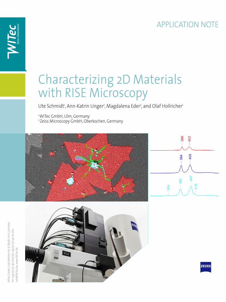
The most prominent Raman bands of mono- and bi-layer graphene are the G band at 1582 rel.cm-1 and the G´ band at about 2700 rel.cm-1. In the case of a disordered sample or at the edge of a graphene sample, the so-called disorder-induced D band arises at around 1350 rel.cm-1. From these three Raman bands most of the electronic and phononic properties of graphene can be derived [11]. Furthermore the positions and intensity ratio of IG/IG´ reveal the number of layers in a graphene sheet, whereas the intensity ratio IG/ID shows the degree of disorder in graphene. Fig. 2a shows the SEM image of a twisted bi-layer graphene flake created by chemical vapor deposition on a 300 nm thick Si/SiO2 substrate. The color-coded marks in this image denote positions from which single Raman spectra were acquired (Fig. 2b). The red spec-trum corresponds to the Raman spectrum of monolayer graphene according to the position and intensity of the G band, the narrow shape and the blue-shifted G´ band. The presence of the D band in this spectrum indicates that the monolayer has a high defect density. In the blue spectrum the intensity of the G band is much higher than the red-shifted intensity of the G´ band corresponding to an AB stacked double layer of graphene[9]. The green spectrum, measured on triple-layer graphene shows a narrow G´ band, which corresponds to an ABA stacking[12]. Thus, the gray shades in the SEM image correspond mainly to an increase in the number of graphene layers, indicated by the intensity of the G band in the Raman spectra. With conventional Raman in SEM, which only
Figure 2: Surface sensitive secondary electron SEM image of twisted bi-layer graphene acquired with the Inlens Duo detector under high vacuum conditions at 2 kV acceleration voltage and color-coded Raman spectra acquired from the marked positions in the SEM image. Each spectrum was acquired with an integration time of 500 ms at 2 mW laser power.
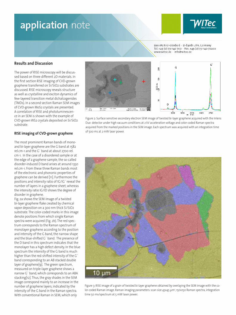
Figure 3: RISE image of a grain of twisted bi-layer graphene obtained by overlaying the SEM image with the co-lor-coded Raman image. Raman imaging parameters: scan size 45x45 µm2, 150x150 Raman spectra, integration time 50 ms/spectrum at 5 mW laser power.

allows for the acquisition of single Raman spec-tra, further analysis of graphene is not possible.Raman imaging of the same sample area re-veals far more details about the electronic and phononic properties of the double-layer gra-phene. The RISE image (Fig. 3) shows that the entire substrate surface is covered by graphene and that there are zones of different layers as revealed by the measured G and G´ Raman bands for graphene. By analyzing the intensity and full width at half maximum (FWHM) of these two characteristic Raman bands, it is possible to determine the stacking order and twist angle of the analyzed twisted double-lay-er graphene grain [7-9]. Fig. 4 shows the variations in peak intensities of IG/IG´ and changes of the FWHM of the G´ Raman band together with the associated variations of the twist angles and stacking orders. To highlight these peak intensity variations and shifts, the Raman spectrum of mono-layer graphene is added as a dashed
states and activates phonons in the interior of the graphene Brillouin zone. By controlling the twist angle between two graphene layers, the electronic and optical properties of twisted double-layer graphene can be modified to specific needs.
line. The correlations of Raman bands and twist angles are summarized in table 1. The interference between two rotated graphene layers generates a superlattice with an angle dependent wavevector that gives rise to van Hove singularities in the electronic density of
IG I (ML) 2ML 2Ml 2ML 2ML >> ML >> ML
IG, I (ML) < ML >> ML ~ ML < ML ~ ML >> ML
FWHM G, ML > ML 2ML >> ML
Raman bands[rel. cm-1]
--- R` @ 1625 --- --- --- R @ 1514 ///
Twist Angle Θ [degree]
--- 3 - 8 > 20 ~ AB 0 - 3 12 Multilayer
Table 1: Correlation of graphene Raman band intensities with the twist angle between double-layers graphene.ML = intensity of G or G´ Raman band corresponding to a monolayer graphene.R`= Raman band which arises only at small rotation angle between the double layer of graphene.R = resonant Raman band which arises at a rotation angle of 12 degrees when the double- layers graphene are excited at 532 nm.
Figure 4: RISE images and Raman spectra highlighting areas with different stacking orders and twist angles. As reference the Raman spectrum of monolayer graphene is shown as dashed line in each spectrum.

Fig. 5: Surface sensitive secondary electron image of a large monolayer graphene sample acquired with the Inlens Duo detector at 1 kV acceleration voltage.
A practical implementation of graphene requires the development of technologies for growing large graphene samples of high quali-ty. A review of the various CVD growth methods is provided in reference [13]. The size and quality of such monolayer graphene can be studied using RISE microscopy.
Fig. 5 shows the SEM image of a large scale pro-duced monolayer of graphene CVD-deposited onto Cu and transferred to a 300 nm thick Si/SiO2 substrate using a PMMA interface. During the transfer process, defects are induced in the graphene monolayer which can be visualized with the SEM. Beside the dark cracks, small dark regularly shaped areas are visible, which corres-pond to double layers of graphene. In the bright areas of this SEM image areas with wrinkles are visible. A color-coded Raman image acquired from an area of 20x20 µm2 is shown in Fig. 6a together with the corresponding spectra in Fig. 6b. The RISE image is presented in Fig. 7. The intensity ratio of IG/IG´ clearly identifies the dark regularly shaped areas as double layers of graphene (pink spectrum in Fig. 6a). Green colored areas in the Raman image from Fig. 6b denote positions with a high density of wrinkles in the SEM image and a lower intensity ratio of IG/ID peaks. The red and blue colored areas and spectra describe a monolayer of graphene. The small difference in spectra is associated only with a slight red shift of the blue spectrum, which may be associated with different stress-zones in the graphene layer.
Figure 6: Color-coded Raman image of a large mo-nolayer graphene sample (b) and the corresponding Raman spectra (a) evaluated from a spectral array of 100x100 Raman spectra acquired from an area of 20x20 µm2, with an integration time of 200 ms/spectrum at 2 mW laser power.
ba
Figure 7: RISE image of the large monolayer graphene sample obtained by overlaying the Raman image from Fig. 6a onto the SEM image from Fig. 5.

c
ba
d
RISE imaging of MoS2
CVD-grown monolayers of MoS2 form triangu-lar two-dimensional crystals. Twin crystals of MoS2 on SiO2/Si appear in the SEM image as star-shaped forms (Fig. 8a).
The Raman spectra of a MoS2 monolayer show the characteristic E‘/E2g and A‘1/A1g Raman band modes of MoS2 at 386 and 403 rel.cm-1, respectively (Fig. 8b). With an increasing num-ber of layers the two Raman bands drift apart due to in-plane and out-of-plane (inter-layer) vibrations. Here the red spectrum indicates the monolayer of MoS2, while the blue and aqua spectra signify double and multi-layer MoS2. The green spectrum is associated with edges and defects, respectively.
The spectral information was used to create a Raman image which was overlaid onto the SEM image to result in a RISE image (Fig. 8c).
The grain boundaries visible in the SEM image correlate perfectly with the areas where Raman signals indicate crumpled or overlapping edges, highlighting the effectiveness of RISE imaging for characterizing MoS2 crystals (Fig. 8d).
Figure 8: Secondary electron image of MoS2 crystals imaged with the Chamber SE detector at 2 kV acceleration voltage under high vacuum conditions (a), Raman spectra evaluated from a spectral array of 100x80 Raman spectra acquired from an area of 22x18 µm2, with an integration time of 50 ms/spec-trum at 5 mW laser power (b), RISE image of MoS2 crystals (c) and high resolution RISE image of the grain boundaries between single MoS2 crystals (d).

RISE imaging of WS2
Here we show the analysis and RISE imaging of WS2 crystals. The high-resolution SEM images were acquired under low vacuum conditions at 5 kV acceleration voltage using the Inlens Duo detector and the secondary electron (SE) detector, respectively (Fig. 9 a, b). Both SEM images show the typical triangular shape of the WS2 crystals. In the SEM image acquired with the Inlens Duo detector, the WS2 crystals appear as bright triangles, whereas the SE detector shows these crystals as dark material. Furthermore, the Inlens Duo detector is more sensitive to the thickness of the material, revealing defects or additional layers within the crystals.
The Raman spectrum acquired with the 532 nm excitation laser (Fig. 10a) shows a strong WS2 Raman signal at 350 rel.cm-1 [14]. Researchers were able to divide this peak into three sub-pe-aks [15]. They associated a signal at 344 rel.cm-1 with the in-plane E‘/E2g Raman mode. The out-of-plane A‘1/A1g Raman band appears at the same relative wavenumber of 417 rel. cm-1 as in the monolayer of MoS2. Using this spectral band a Raman intensity map was generated that highlights a quantified increase of the Raman band intensity in the region of a double layer (green area Fig. 10b). All the other crystals appear homogenous as monolayers of WS2. By combining the SEM and the Raman images, the RISE image from Fig. 10c can be generated.
Figure 10: Raman spectrum of WS2 (a) and Raman intensity map of the Raman band at 717 rel. cm-1 (b). Raman image acquisition parameters: 100x100 Raman spectra acquired from an area of 15x15 µm2, with an integration time of 60 ms/spec-trum at 2 mW laser power. (c) RISE image of the WS2 crystals.
a b
Figure 9: SEM images of WS2 crystals acquired with the Inlens Duo (a) and the Chamber SE (b) detectors at 5 kV acceleration voltage.
c
a b
For this group of 2D materials the informa-tion obtained through the combination of techniques is even more valuable as the transi-tion of indirect to direct semiconductor when going to a single layer gives rise to pronounced photoluminescence (PL) [4]. Fig. 11a shows the two extreme PL spectra acquired from the ana-lyzed sample area together with the PL image (Fig. 11b).
The WS2 crystals display strong PL in the range 630-650 nm, with variations in position with the size of the analyzed crystals. An overlay of the SEM images with the PL image is shown in Fig. 12. This strong PL is observed only in the single monolayer crystals due to the direct band gap in the monolayer of WS2. Figure 11: PL spectra acquired from WS2 crystals (a) and the distribution of the PL shift over the analyzed sample
area (b). The PL spectra were acquired from an area of 15x15 µm2, with an integration time of 35 ms/spectrum at 2 mW laser power.
ba
Figure 12: Overlay of the two SEM images from Fig. 9 with the PL image.
ba

Summary
ZEISS Sigma 300 RISE is a versatile tool for high resolution SEM imaging of sensi-tive 2D materials due to its ability to acquire images at low acceleration voltages and low beam currents. Furthermore, charging and beam damage can be easily prevented by working under low vacuum conditions without losing high resolu-tion capabilities. By attaching the confocal Raman microscope to a standard port of the vacuum chamber an easy workflow between SEM and Raman imaging is assured. The added value of Raman and PL imaging for the characterization of 2D materials is presented in this study.
REFERENCES1. K. S. Novoselov, A. K. Geim, S. V. Morozov, D. Jiang, Y. Zhang, S. V. Dubonos, I. V. Grigorieva and A. A. Firsov,
Science 306 (2004) 666.2. Geim A. K., Grigorieva I. V., Nature 499 (2013) 419.3. M. Xu, T. Liang, M. Shi and H. Chen, Chem. Rev. 113 (2013) 3766.4. J.A. Wilson & A.D. Yoffe , Advances in Physics, 18-73 (1969)193.5. Koppens F. H. L., Nueller T., Avouris P., Ferrari A.C., Vitiello M. S., Polini M., M. Nat. Nano 9 (2014) 780.6. You Y., Ni Z., Yu T., Shen Z., Appl. Phys. Letters 93 (2008) 1.7. Ohta, T. Becheem, J.T. Robinson, G.L. Kellogg, Phys. Rev B 85 (2012) 75415.S. D. Costa, J. E. Weis, O. Frank, M.
Kalbac, Carbon 98 (2016) 592.8. Y. Chen, L. Meng, W. Zhao, Z. Liang, X. Wu, H. Nan, Z. Wu, S. Huang, L. Sun, J. Wang, and Z. Ni, Phys. Chem.
Chem. Phys. 16 (2014) 21682.9. Maria O’Brien, Niall McEvoy, Damien Hanlon, Toby Hallam, Jonathan N. Coleman, G. S. Duesberg, Scientific
Reports 6 (2016) 19476.10. L.M. Malarda, M.A. Pimenta, G. Dresselhaus, M.S. Dresselhaus, Physics Reports 473 (2009) 51.11. C. Cong, T. Yu, K. Sato, J. Shang, R. Saito, G. F. Dresselhaus, M. S. Dresselhausz, ACS Nano 5 (2011) 8760.12. I. V. Antonova, Physics-Uspekhi 56 (2013) 1013. 13. Y. Wang, C. Cong, W. Yang, J. Shang, N. Peimyoo, Y. Chen, J. Kang, J. Wang, W. Huang, T. Yu. Nano Research 8
(2015) 2565.14. N. Peimyoo, J. Shang, C. Cong, X. Shen, X. Wu, E. K. L. Yeow, Ting Yu, ACS Nano 7 (2013) 1095.

WITec HeadquartersWITec GmbHLise-Meitner-Str. 6D-89081 Ulm. GermanyPhone +49 (0)731 140700Fax +49 (0)731 [email protected]
WITec North AmericaWITec Instruments Corp.130G Market Place Blvd.Knoxville. TN 37922. USAPhone +1 865 984 4445Fax +1 865 984 [email protected]
WITec South East AsiaWITec Pte. Ltd.25 Int. BusinessPark#03-59A German CentreSingapore 609916Phone +65 9026 [email protected]
WITec ChinaWITec Beijing Representative OfficeUnit 507, landmark Tower 18 North Dongsanhuan RoadBeijing, PRC., 100004Phone + 86 (0) 10 6590 [email protected]/cn
WITec JapanWITec K.K.Mita 2-3227, Chome, Tama-kuKawasaki/shi, Kanagawa-ken 214-0034JapanPhone +81 44 19 773keiichi.nakamoto@witec/instruments.bizwww.witec.de/jp