characterization of heavily doped polysilicon films for .... jmm... · j. micromech. microeng. 19...
TRANSCRIPT
IOP PUBLISHING JOURNAL OF MICROMECHANICS AND MICROENGINEERING
J. Micromech. Microeng. 19 (2009) 125029 (8pp) doi:10.1088/0960-1317/19/12/125029
Characterization of heavily dopedpolysilicon films for CMOS-MEMSthermoelectric power generatorsJin Xie1, Chengkuo Lee1,2, Ming-Fang Wang1, Youhe Liu1 andHanhua Feng1
1 Institute of Microelectronics, A∗STAR (Agency for Science, Technology and Research), 11 SciencePark Road, Singapore Science Park II, Singapore 1176852 Department of Electrical and Computer Engineering, National University of Singapore, 4 EngineeringDrive 3, Singapore 117576
E-mail: [email protected] and [email protected]
Received 4 September 2009, in final form 15 October 2009Published 16 November 2009Online at stacks.iop.org/JMM/19/125029
AbstractThis paper presents the material characterization of boron- and phosphorus-doped LPCVDpolysilicon films for the application of thermoelectric power generators. Electrical resistivity,Seebeck coefficient and thermal conductivity of polysilicon films doped with doses from 4 ×10¹⁵ to 10 × 1015 at cm−2 have been measured at room temperature. Specific contactresistance between polysilicon and aluminum is studied and nickel silicidation is formed toreduce the contact resistance. The overall thermoelectric properties, as characterized by thefigure of merit, are reported for polysilicon doped with different doping concentrations. Forthe most heavily doping dose of 10 × 1015 at cm−2, figure of merit for p- and n-typepolysilicon is found as 0.012 and 0.014, respectively. Based on the characterization results, aCMOS compatible thermoelectric power generator composed of boron- and phosphorus-dopedpolysilicon thermopiles is fabricated. When 5 K temperature difference is maintained acrosstwo sides of a device of size of 1 cm2, the output power is 1.3 μW under a matched electricalresistance load.
1. Introduction
As a kind of energy harvesting device, thermoelectricpower generators (TPGs) have been investigated togenerate electricity from temperature difference due to thethermoelectric Seebeck effect. One of the scenarios isharvesting body heat as an alternative power source to enableapplications such as self-sustained wearable electronics, bodyarea sensor networks, etc [1, 2]. A thermocouple is madeof two different thermoelectric bars joined at one end. TPGsare composed of a large number of thermocouples which areelectrically connected in series. Thermoelectric materials arecharacterized by a dimensionless figure-of-merit parameter(ZT ):
ZT = α2
ρλT , (1)
where α is the Seebeck coefficient, ρ is the electrical resistivity,λ is the thermal conductivity and T is the temperature.
Currently, most commercial TPGs [3] use Bi2Te3 asthermoelectric material due to its large thermoelectric figureof merit. However, Bi2Te3 and its alloy are not CMOScompatible materials, which means Bi2Te3 materials basedapproaches cannot provide a TPG to be monolithicallyintegrated on microelectronics and fabricated in normalCMOS manufacturing lines. Integration of TPGs withmicroelectronics to form a self-sustained system-on-chipdevice is a goal receiving a lot of research attention. HavingTPGs fabricated by the standard CMOS process is necessaryto achieve such a goal.
On the other hand, high thermoelectric performance hasbeen found in single crystal silicon nanowires recently [4, 5],however, great challenges exist to fabricate TPGs with siliconnanowires, such as electrical connection of a large number
0960-1317/09/125029+08$30.00 1 © 2009 IOP Publishing Ltd Printed in the UK

J. Micromech. Microeng. 19 (2009) 125029 J Xie et al
of p- and n-type silicon nanowires in series. Thus, theresearch on silicon nanowires for thermoelectric applicationsis still at its infant stage. Most of the publications inthis field are related to material characterization. Dopedpolysilicon has attracted wide research interest for applicationsof TPGs due to its CMOS compatibility and widely availableprocessing capability. Various TPGs based on p- and n-type doped polysilicon have been proposed and developed,but most of them have poor output power due to thelow figure of merit of polysilicon [6–8]. To improve theperformance of the TPGs, thermoelectric properties of dopedpolysilicon need to be characterized and optimized. In the late1990s, research efforts were made to investigate the materialproperties of polysilicon and other CMOS materials in viewof promising applications of various microelectromechanicalsystems (MEMS) based CMOS sensors [9], e.g. thermopiles,Pirani sensors, microbolometers, etc. For example, Paul et algave the first overview of measured thermophysical propertiesof gate polysilicon and capacitor thin films [10], and vonArx et al fabricated test structures to measure the Seebeckcoefficient [11] and thermal conductivity [12] of polysiliconof commercial CMOS IC processes in a wide temperaturerange from 120 to 400 K. All these authors focused onthe measurement of polysilicon film produced by standardCMOS processes, and did not discuss the effect of dopingconcentration. Boutchich et al [13] characterized Seebeckcoefficient of boron and phosphorus heavily doped LPCVDpolysilicon films with different doses in the temperaturerange of 293–373 K. McConnell et al [14] provided athermal modeling for polysilicon and verified the modelingby measuring thermal conductivity at different processingconditions and dopant concentrations. Later on, Strasserdemonstrated micromachined TPGs using thermocouplesmade of polysilicon and characterized the materials at differentdoping concentrations in 2004, but figure of merit was notdiscussed in this paper in order to optimize the materialproperties for TPGs [6]. Additionally, PolySiGe as anotherCMOS compatible material has also been characterized for itsthermoelectric properties [15, 16].
This paper presents the characterization of materialproperties of boron- and phosphorus-doped polysilicon tooptimize the performance of TPGs. The characterizedproperties include electrical resistivity, specific contactresistance, Seebeck coefficient and thermal conductivity. Thispaper first studies how these properties are affected by dopingdoses in a range from 4 × 10¹⁵ to 10 × 1015 at cm−2. Specialtest structures are designed to characterize the above propertiesof polysilicon films at room temperature. Figure of meritof doped polysilicon for each doping dose is discussed andcompared with the values from the literature. Based onthe optimized thermoelectric material properties, a CMOScompatible TPG using p- and n-doped polysilcon thermopilesis fabricated, and the output power from the TPG is measured.Our approach shows optimized polysilicon TPG performance,which is better than reported data from the other groups.
Table 1. Implant energy for doping polysilicon layers.
Implant energy (keV)
Doping dose (at cm−2) Boron doped Phosphorus doped
4 × 10¹⁵ 70 1006 × 1015 70 1308 × 1015 80 160
10 × 1015 80 180
2. Fabrication and characterization
To prepare polysilicon samples for testing, 700 nm thickpolysilicon layers are grown at 580 ◦C in furnace bylow-pressure chemical vapor deposition (LPCVD). Thepolysilicon layers are partially implanted by boron (p-type)and phosphorus (n-type) from 4 × 10¹⁵ to 10 × 1015 at cm−2
doses. The implant energy for each group doses is shown intable 1. Afterward, the doped polysilicon layers are annealedin furnace at 1000 ◦C for 30 min to activate dopants and obtain auniform doping profile through the whole thickness and repairthe defects in the crystalline structure.
2.1. Electrical resistivity and specific contact resistance
Low electrical resistivity of polysilicon and low specificcontact resistance between polysilicon and metals is highlydesired in a micromachined TPG composed of a large numberof thermocouples. The electrical resistivity is determinedby the van-der-Pauw structure, and the measured values atdifferent doping doses at room temperature are shown infigures 1(a) and (b). It is found that the higher the doping dose,the lower is the electrical resistivity. The electrical contactresistance is derived via the Kelvin structure [17], as shownin figure 2(a). An effective way to reduce contact resistanceis creating nickel silicidation layer between polysilicon andmetal. The process of formation of nickel silicidaitonis described as follows: after deposition and pattern ofpolysilicon, metal (here Al/TaN) and oxide dielectric layer,135 A thick nickel is deposited by sputtering; and then thesilicidation step is done by a thermal reaction using rapidthermal processing (RTP) at 480 ◦C for 30 s; finally, theunreacted nickel is etched using H2SO4:H2O2 = 4:1 solutionat 90 ◦C for 5 min. Transmission electron microscopy (TEM)analyzes that the component of nickel silicidation is NiSi(as shown in figure 2(b)), which has lower resistivity thanother forms of nickel silicidation do, such as Ni2Si and NiSi2[18, 19]. Without nickel silicidation, the specific contactresistance is 360 � μm2 for p-type and 477 � μm2 for n-typepolysilicon. However, with the formation of nickel silicidationbetween polysilicon and aluminum alloy, the specific contactresistance is only about one quarter of the values, i.e.,95 � μm2 for p-type and 123 � μm2 for n-typepolysilicon.
2.2. Seebeck coefficient
Seebeck coefficient was measured by a planar test structure,as shown in figure 3. The polysilicon stripe sample being
2

J. Micromech. Microeng. 19 (2009) 125029 J Xie et al
(a) (b)
Figure 1. (a) Van de Pauw structure and (b) electrical resistivity of polysilicon at different doping doses.
(a) (b)
Figure 2. (a) Kelvin structure and (b) TEM of NiSi silicidation between polysilicon and Al/TaN.
characterized has a length of 670 μm and a width of 30 μm.It is contacted to aluminum at its two ends (pads 5 and 6). A110 μm × 20 μm polysilicon heater (pads 11 and 12) is placed20 μm away from the contact of the hot junction. Two 5 μmwide temperature monitors made of aluminum are placed overthese two contacts. The temperature monitors are integratedin a four-point measurement configuration (pads 1, 2, 3, 4and 7, 8, 9, 10) enabling accurate measurements of smallresistance changes and, thus, small temperature variations.When applying current to the heating resistor, the temperatureof the hot and cold contacts of the polysilicon sample wasincreased from T0 to Th and Tc, respectively. The Seebeckcoefficient was expressed by
α| Th+Tc2
= U
Th − Tc= U
�T, (2)
where U is thermovoltage between the two ends of polysilicon.The measurement consisted of determining the temperatureincreases �T of each thermistor under a dissipated heat powerand simultaneously measuring the thermovoltage U . Wedetermined �T using the temperature-dependent resistanceR(T ) of the temperature monitors, via their temperaturecoefficient of resistance (TCR) β(T ) defined as
β(T ) = R(T )−1 d
dTR(T ). (3)
For this purpose, R(T ) curves were measured independentlyfor each temperature sensing resistor of each test structure totake into account possible variations in material properties.Resistance R(Ti) was measured at each temperature Ti (i =1, 2, . . . , 19), under stabilized temperature conditions. Fromthe resistance data, values of β(Ti) (i = 2, 3, . . . , 18), werecalculated for each temperature sensing resistor of each teststructure using finite difference, i.e.,
β(Ti) = R(Ti)−1 R(Ti+1) − R(Ti−1)
Ti+1 − Ti−1. (4)
As an example of boron-doped polysilicon with dose of10 × 1015 at cm−2, figure 4 shows the temperature-dependentresistance of the aluminum resistors and its TCR. At T =300 K, the electrical resistance of the aluminum-based alloyresistor was 0.166 � and β was 3.8 × 10⁻³ K−1. Accordingto the dimension of the resistor, the electrical resistivity of thealuminum-based alloy was calculated as 3.15 × 10⁻⁸ � m atT = 300 K.
For the thermovoltage measurements, a heating currentIh was passed through the heating resistor. The resultingresistance change �R of the temperature monitors was
3

J. Micromech. Microeng. 19 (2009) 125029 J Xie et al
Figure 3. Test structure to determine the Seebeck coefficient.
260 280 300 320 340 360
0.14
0.15
0.16
0.17
0.18
0.19
0.20
0.21
Temperature (K)
Re
sist
an
ce( Ω
)
0.000
0.001
0.002
0.003
0.004
0.005
TC
R(1
0-3K
-1)
Figure 4. Temperature-dependent resistance and TCR of thealuminum temperature monitors.
measured simultaneously. The temperature increases �T
were obtained using
�T = 1
β
�R
R. (5)
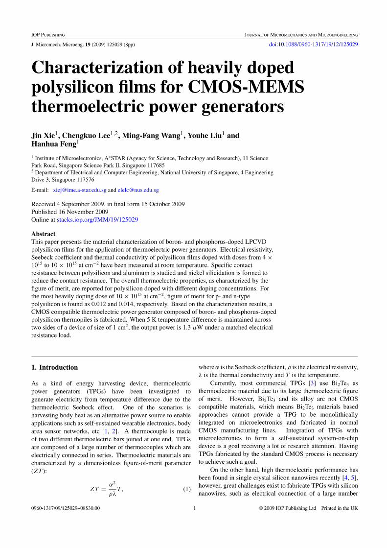
Simultaneously with the �R measurement we recorded thethermovoltage U . For the example of boron-doped polysiliconwith 10 × 1015 at cm−2 doses, figure 5 shows the experimentaldata of the thermovoltage and temperature increases as afunction of the heating current Ih at T0 = 300 K. Based onthe raw data, the Seebeck coefficient α of the polysilicon wascalculated using equation (2). Figure 6 shows the measuredSeebeck coefficient at room temperature for both doped p-typeand n-type polysilicon with different doping doses.
2.3. Thermal conductivity
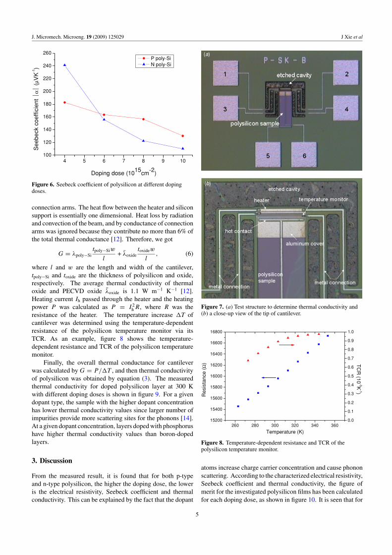
Thermal conductivity was determined by a cantilevercomposed of three layers: thermal oxide, LPCVD polysiliconand PECVD oxide, as shown in figure 7. A 100 μm wideand 270 μm long beam with four narrow arms is suspended
0 20 40 60 800
5
10
15
20
25
30
ΔΤh
ΔΤc
U
Ih (mA)
ΔT(K
)
0
2
4
6
8
10
12
14
U(m
V)
Figure 5. Thermovoltage as a function of heater current.
over a cavity. Two contacts made of aluminum (pads 5 and6) are used to measure the thermally generated voltage fromthe polysilicon sample. The hot contact is placed 23 μm awayfrom the tip end of the cantilever, and the cold contact is onthe substrate. Two resistors made of polysilion are integratedinto the tip of the cantilever. The resistor (pads 1 and 2)close to the end of the beam is used as a heater, which haslength of 92 μm, width of 6 μm and resistance of 2635 �
at T = 300 K. The other resistor (pads 3 and 4) is used astemperature monitor, with total length of 280 μm and widthof 1 μm. The temperature distribution over the top of thetwo resistors is homogenized with an integrated rectangularcover made of aluminum. This minimizes the temperaturedifference between the hot contact and temperature monitor.The cantilever was released by isotropic silicon etching withSF6 gas. When a power P was dissipated in the heater, thetemperature on the cantilever tip was increased by �T withrespect to the substrate temperature. The heating power P and�T are related by P = G · �T , where G denotes the overallthermal conductance of the structure, including cantilever and
4
J. Micromech. Microeng. 19 (2009) 125029 J Xie et al
4 5 6 7 8 9 10100
120
140
160
180
200
220
240
260
Se
ebe
ckco
eff
icie
nt
⏐α⏐
(μV
K-1)
Doping dose (1015cm-2)
P poly-SiN poly-Si
Figure 6. Seebeck coefficient of polysilicon at different dopingdoses.
connection arms. The heat flow between the heater and siliconsupport is essentially one dimensional. Heat loss by radiationand convection of the beam, and by conductance of connectionarms was ignored because they contribute no more than 6% ofthe total thermal conductance [12]. Therefore, we got
G = λpoly−Sitpoly−Siw
l+ λoxide
toxidew
l, (6)
where l and w are the length and width of the cantilever,tpoly−Si and toxide are the thickness of polysilicon and oxide,respectively. The average thermal conductivity of thermaloxide and PECVD oxide λoxide is 1.1 W m−1 K−1 [12].Heating current Ih passed through the heater and the heatingpower P was calculated as P = I 2
h R, where R was theresistance of the heater. The temperature increase �T ofcantilever was determined using the temperature-dependentresistance of the polysilicon temperature monitor via itsTCR. As an example, figure 8 shows the temperature-dependent resistance and TCR of the polysilicon temperaturemonitor.
Finally, the overall thermal conductance for cantileverwas calculated by G = P/�T , and then thermal conductivityof polysilicon was obtained by equation (3). The measuredthermal conductivity for doped polysilicon layer at 300 Kwith different doping doses is shown in figure 9. For a givendopant type, the sample with the higher dopant concentrationhas lower thermal conductivity values since larger number ofimpurities provide more scattering sites for the phonons [14].At a given dopant concentration, layers doped with phosphorushave higher thermal conductivity values than boron-dopedlayers.
3. Discussion
From the measured result, it is found that for both p-typeand n-type polysilicon, the higher the doping dose, the loweris the electrical resistivity, Seebeck coefficient and thermalconductivity. This can be explained by the fact that the dopant
(a)
(b)
Figure 7. (a) Test structure to determine thermal conductivity and(b) a close-up view of the tip of cantilever.
260 280 300 320 340 36015200
15400
15600
15800
16000
16200
16400
16600
16800
Temperature (K)
Res
ista
nce
(Ω)
0.0
0.1
0.2
0.3
0.4
0.5
0.6
0.7
0.8
0.9
1.0
TC
R(1
0-3K
-1)
Figure 8. Temperature-dependent resistance and TCR of thepolysilicon temperature monitor.
atoms increase charge carrier concentration and cause phononscattering. According to the characterized electrical resistivity,Seebeck coefficient and thermal conductivity, the figure ofmerit for the investigated polysilicon films has been calculatedfor each doping dose, as shown in figure 10. It is seen that for
5

J. Micromech. Microeng. 19 (2009) 125029 J Xie et al
Table 2. Summarization of characterization of thermoelectric properties for polysilicon and polySiGe at T = 300 K.
Electrical Seebeck Thermal conductivity FigureMaterial resistivity (� μm) coefficient (μV K −1) (W m−1 K−1) of merit Reference
Polysilicon p 22.1 103 31.2 0.005 [6]n 8.1 −57 31.5 0.004p 13.7 130 28.4 0.012 This work (for dose
of 10 × 1015 at cm−2)n 8.9 −110 29.7 0.014
PolySiGe p 28.9 131 4.7 0.037 [15]n 29.2 −179 5.1 0.061p 11 35 ∼3.5 0.01–0.02 [16]n 62 −190 ∼3.5 0.04–0.05
4 5 6 7 8 9 10
26
28
30
32
34
36
38
40
P poly-SiN poly-Si
The
rmal
cond
uctiv
ity(W
m-1K
-1)
Doping dose (1015cm-2)
Figure 9. Thermal conductivity of polysilicon at different dopingdoses.
p-type polysilicon, the most heavily doped (10 × 1015 at cm−2)has the highest figure of merit, while doping dose of 4 ×10¹⁵ at cm−2 is the case of highest figure of merit for then-type polysilicon. This is due to the fact that the Seebeckcoefficient of n-type polysilicon with doping dose of 4 ×10¹⁵ at cm−2 is much higher than the value of the other dopingconcentrations, while for p-type at this doping concentrationthe Seebeck coefficient does not increase so much. However,the electrical resistivity at doping dose of 4 × 10¹⁵ at cm−2
is about twice the value at 10 × 1015 at cm−2 for both p-typeand n-type polysilicon. When using TPGs to supply powerfor electronics, the maximum output power is achieved undermatched load condition, i.e. the load resistance connected tothe generator equals the internal electrical resistance of thegenerator. Since TPGs based on polysilicon usually havevery high internal electrical resistance which is at the levelof tens of megaohm [6, 7], it is preferred to make the electricalresistivity of polysilicon as low as possible. As a trade-offbetween figure of merit and electrical resistivity, the mostheavily doped polysilicon, i.e., 10 × 1015 at cm−2, is chosenin fabrication of TPGs. Thermoelectric properties and figure ofmerit of polysilicon and polySiGe reported in the literature aresummarized in table 2. Generally, polySiGe has a much lowerthermal conductivity, and thus higher figure of merit, than
4 6 8 100.000
0.005
0.010
0.015
0.020
0.025
Doping dose ( ×1015 at/cm2)
Fig
ure
of
me
ritZ
T
P-type polysiliconN-type polysilicon
Figure 10. Figure of merit for polysilicon doped with differentdoses at T = 300 K.
polysilicon. However, the electrical resistivity of polySiGe ishigher than polysilicon, which causes higher internal electricalresistance of power generator based on polySiGe.
Based on the characterization results, a CMOS compatibleTPG has been designed and fabricated, as shown in figure 11.The TPG consists of p- and n-doped polysilicon thermopiles,and top and bottom cavities are created to optimize heatflux through the thermal legs. The detailed fabrication stepsand materials were presented in [20]. The generator of area1 cm2 consists of 125 144 thermocouples and has an internalelectrical resistance of 36 × 106 �. A graph of the outputpower per area versus the temperature difference for thefabricated generator is displayed in figure 12. It is foundthat when 5 K difference is maintained across two sides ofthe device of size 1 cm2 and under a matched electricalresistance load, the output power is 1.3 μW, which is 1.3 timeshigher than the power from the polysilicon TPG reported byInfineon [6]. Recently Yang et al have also reported a CMOSbased TPG with output power of about 1 μW from 1 cm2
active area and under 5 K difference [8]. Our approach showsoptimized polysilicon TPG performance which is better thanreported data from the other groups.
6

J. Micromech. Microeng. 19 (2009) 125029 J Xie et al
(a)
(b) (c )
Figure 11. Thermoelectric power generator based on doped polysilicon: (a) schematic view, (b) top view and (c) cross-sectional view.
0 1 2 3 4 5
0.0
0.2
0.4
0.6
0.8
1.0
1.2
1.4
Ou
tpu
tp
owe
r(μ
W/c
m2)
Temperature difference across chip (K)
Figure 12. Output power versus temperature difference across thechip.
4. Conclusion
Heavily doped boron and phosphorus LPCVD polysiliconfilms with different doping doses have been characterized fortheir thermoelectric performance. Test structures are designedto characterize the electrical resistivity, specific contactresistance, Seebeck coefficient and thermal conductivityat room temperature. The electrical resistivity, Seebeckcoefficient and thermal conductivity decrease with increasing
doping dose. The formation of nickel silicidiaton betweenpolysilicon and metal greatly reduces the contact resistance.Values of the figure of merit for the polysilicon film doped bydifferent doses are reported. Considering the requirement oflow total electrical resistance of the thermoelectric generator,the most heavily doped (10 × 1015 at cm−2) polysilicon filmis chosen for the fabrication of the power generator, and thefigures of merit for the chosen p- and n-type polysilicon aremeasured as 0.012 and 0.014, respectively. These resultsprovide good data reference to fabricate thermoelectric powergenerator of optimal design with high output power.
Acknowledgment
The authors and C Lee, PI of A∗STAR HOME 2015 NationalResearch Programme (SERC grant no. 0621150043), wouldlike to thank A∗STAR HOME 2015 National ResearchProgramme for the funding of this project and in-kindcontribution from Institute of Microelectronics, A∗STAR.
References
[1] Leonov V, Torfs T, Fiorini P and Hoof C V 2007Thermoelectric converters of human warmth forself-powered wireless sensor nodes IEEE Sensors J.7 650–7
[2] Torfs T, Leonov V and Vullers R J M 2007 Pulse oximeterfully powered by human body heat Sensors Transducers J.80 1230–38
7

J. Micromech. Microeng. 19 (2009) 125029 J Xie et al
[3] Bottner H, Nurnus J, Gavrikov A, Kuhner G, Jagle M,Kunzel C, Eberhard D, Plescher G, Schuber A andSchlerth K H 2004 New thermoelectric components usingmicrosysterm technologies J. Microelectromech. Syst.13 414–20
[4] Hochbaum A I, Chen R, Delgado R D, Liang W, Garnett E C,Najarian M, Majumdar A and Yang P 2008 Enhancedthermoelectric performance of rough silicon nanowiresNature 451 163–7
[5] Boukai A I, Bunimovich Y, Jamil T-K, Yu J-K, Goddard W Aand Heath J R 2008 Silicon nanowires as efficientthermoelectric materials Nature 451 168–71
[6] Strasser M, Aigner R, Lauterbach C, Sturm T F, Franosch Mand Wachutka G 2004 Micromachined CMOSthermoelectric generators as on-chip power supply SensorsActuators A 114 362–70
[7] Huesgen T, Woias P and Kockmann N 2008 Design andfabrication of MEMS thermoelectric generators with hightemperature efficiency Sensors Actuators A 145–146 423–9
[8] Yang S M, Lee T and Jeng C A 2009 Development of athermoelectric energy harvester with thermal isolationcavity by standard CMOS process Sensors Actuators A153 244–50
[9] Graf A, Arndt M, Sauer M and Gerlach G 2007 Review ofmicromachined thermopiles for infrared detection Meas.Sci. Technol. 18 R59–75
[10] Paul O, von Arx M and Baltes H 1995 Process-dependentthermophysical properties of CMOS IC thin films Proc.Transducers (Stockholm, Sweden, 25–29 Jun. 1995)pp 178–81
[11] von Arx M, Paul O and Baltes H 1997 Test structures tomeasure the Seebeck coefficient of CMOS IC polysiliconIEEE Trans. Semicond. Manuf. 10 201–8
[12] von Arx M, Paul O and Baltes H 2000 Process-dependentthin-film thermal conductivities for thermal CMOS MEMSJ. Microelectromech. Syst. 9 136–45
[13] Boutchich M, Ziouche K, Godts P and Leclercq D 2002Characterization of phosphorus and boron heavilydoped LPCVD polysilicon films in the temperaturerange 293–373 K IEEE Electron Device Lett.23 139–41
[14] McConnell A D, Uma S and Goodson K E 2001 Thermalconductivity of doped polysilicon layers J.Microelectromech. Syst. 10 360–9
[15] Wijngaards D D L and Wolffenbuttel R F 2002Thermo-electric characterization of APCVD polySi0.7Ge0.3
for IC-compatible fabrication of integrated lateral Peltierelements IEEE Electron Device Lett. 23 139–41
[16] Wang Z, Fiorini P, Leonov V and Hoof C V 2009Characterization and optimization of polycrystallineSi70%Ge30% for surface micromachined thermopiles inhuman body applications J. Micromech. Microeng.19 094011
[17] Proctor S J, Linholm L W and Mazer J A 1983 Directmeasurement of interfacial contact resistance, end contactresistance, and interfacial contact layer uniformity IEEETrans. Electron Devices 30 1535–42
[18] Colgan E G, Gambino J P and Hong Q Z 1996 Formation andstability of silicides on polycrystalline silicon Mater. Sci.Eng. R16 43–96
[19] Deng F, Johnson R A, Asbeck P M and Lau S S 1997Silicidation process using NiSi and its device applicationJ. Appl. Phys. 81 8047–51
[20] Xie J, Lee C and Feng H 2009 Design, fabrication andcharacterization of CMOS MEMS based thermoelectricpower generators J. Microelectromech. Syst. at press
8