characterization and failure analysis of silicon...
TRANSCRIPT

Characterization and Failure Analysis Characterization and Failure Analysis of Silicon Devicesof Silicon DevicesCurrent and FutureCurrent and Future
Dieter K. SchroderDieter K. SchroderDept. of Electrical EngineeringDept. of Electrical Engineering
Arizona State UniversityArizona State UniversityTempe, AZTempe, AZ
IntroductionIntroductionBackgroundFailure site location
IDDQ testingLiquid crystalEmission microscopyPicosecond imaging circuit analysisVoltage contrastOptical beam induced resistance change
Physical AnalysisHigh resolution TEMMicroprobing
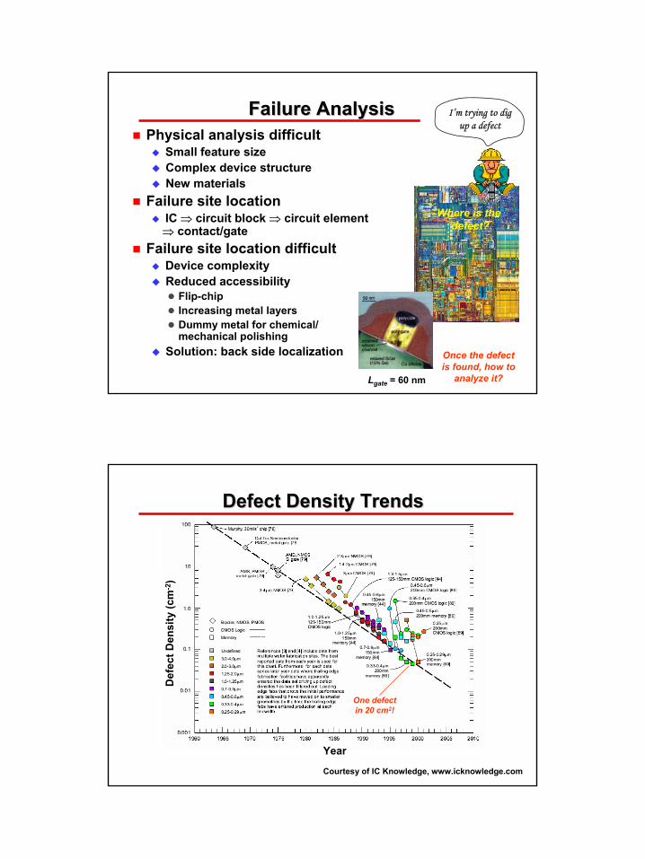
Failure AnalysisFailure AnalysisPhysical analysis difficult
Small feature sizeComplex device structureNew materials
Failure site location IC ⇒ circuit block ⇒ circuit element
⇒ contact/gate Failure site location difficult
Device complexityReduced accessibility
Flip-chipIncreasing metal layersDummy metal for chemical/ mechanical polishing
Solution: back side localization
Where is the defect?
Once the defect is found, how to
analyze it?Lgate = 60 nm
I’m trying to digup a defect
Defect Density TrendsDefect Density Trends
Courtesy of IC Knowledge, www.icknowledge.com
One defectin 20 cm2!
Def
ect D
ensi
ty (c
m-2
)
Year

Failure Site LocationFailure Site LocationIDDQ testingLiquid crystalEmission microscopyPicosecond imaging circuit analysisVoltage contrastOptical beam induced resistance changeMicroprobing
IIDDQDDQ TestingTestingIDDQ
Quiescent drain current flowing from power supply to groundDevice in quiescent state10-9 A range in quiescent stateIncreases due to defectsMainly detects physical defects,is supplemental to logic testing
R. Rajsuman, Iddq Testing for CMOS VLSI, Proc. IEEE 88, 544-566, April 2000;L.C. Wagner, Failure Analysis of Integrated Circuits, Kluwer, Boston, 1999
VDD
Gate OxideShort
MetalBridgingShort
Source-DrainShort
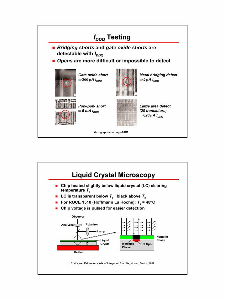
IIDDQDDQ TestingTestingBridging shorts and gate oxide shorts are detectable with IDDQ
Opens are more difficult or impossible to detect
Gate oxide short⇒360 µA IDDQ
Micrographs courtesy of IBM
Poly-poly short⇒5 mA IDDQ
Metal bridging defect⇒5 µA IDDQ
Large area defect(28 transistors)⇒620 µA IDDQ
Liquid Crystal MicroscopyLiquid Crystal MicroscopyChip heated slightly below liquid crystal (LC) clearing temperature Tc
LC is transparent below Tc , black above Tc
For ROCE 1510 (Hoffmann La Roche): Tc = 48°CChip voltage is pulsed for easier detection
L.C. Wagner, Failure Analysis of Integrated Circuits, Kluwer, Boston, 1999
Lamp
Observer
LiquidCrystalIC
Heater
Hot Spot
NematicPhase
IsotropicPhase
PolarizerAnalyzer

Liquid Crystal MicroscopyLiquid Crystal Microscopy
Poly-Si bridge causes hot spotCourtesy of C.G.C. De Kort, Philips Research Laboratories
Bipolar Junction Transistor
Hot spot due to 2.2 mW power dissipation
3.5 mW 2.65 mW 2.2 mW 1.75 mW
Courtesy of N. Nenadovic, DIMES, Delft University
Emission Microscopy (EMMI)Emission Microscopy (EMMI)
Image of circuit is taken in ordinary lightImage of circuit is taken in the dark with circuit powered up; defects appear as bright spotsThe two images are superimposed, showing defect locations on the circuit
C.G.C. de Kort, “Integrated Circuit Diagnostic Tools: UnderlyingPhysics and Applications,” Philips J. Res. 44, 295-327, 1989.
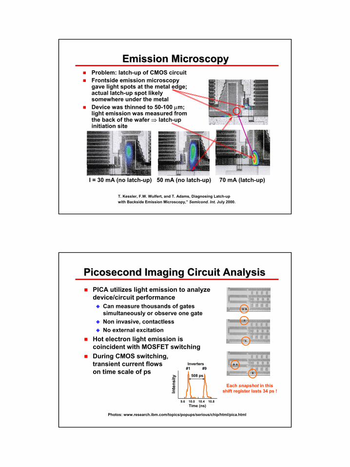
Emission MicroscopyEmission MicroscopyProblem: latch-up of CMOS circuitFrontside emission microscopy gave light spots at the metal edge; actual latch-up spot likely somewhere under the metalDevice was thinned to 50-100 µm; light emission was measured from the back of the wafer ⇒ latch-up initiation site
I = 30 mA (no latch-up) 50 mA (no latch-up)
T. Kessler, F.W. Wulfert, and T. Adams, Diagnosing Latch-upwith Backside Emission Microscopy,” Semicond. Int. July 2000.
70 mA (latch-up)
PicosecondPicosecond Imaging Circuit AnalysisImaging Circuit AnalysisPICA utilizes light emission to analyze device/circuit performance
Can measure thousands of gates simultaneously or observe one gateNon invasive, contactlessNo external excitation
Hot electron light emission is coincident with MOSFET switchingDuring CMOS switching, transient current flows on time scale of ps
Photos: www.research.ibm.com/topics/popups/serious/chip/html/pica.html
Each snapshot in this shift register lasts 34 ps !
9.6 10.0 10.4 10.8Time (ns)
Inte
nsity
Inverters#1 #9
508 ps
PicosecondPicosecond Imaging Circuit AnalysisImaging Circuit Analysis
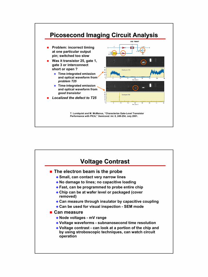
Problem: incorrect timing at one particular output pin; switched too slowWas it transistor 25, gate 1, gate 3 or interconnect short or open ?
Time-integrated emission and optical waveform from problem T25Time-integrated emission and optical waveform from good transistor
Localized the defect to T25
T. Lundquist and M. McManus, “Characterize Gate-Level Transistor Performance with PICA,” Semicond. Int. 8, 249-254, July 2001.
Voltage ContrastVoltage ContrastThe electron beam is the probe
Small, can contact very narrow linesNo damage to lines; no capacitive loadingFast, can be programmed to probe entire chipChip can be at wafer level or packaged (cover removed)Can measure through insulator by capacitive couplingCan be used for visual inspection - SEM mode
Can measureNode voltages - mV rangeVoltage waveforms - subnanosecond time resolutionVoltage contrast - can look at a portion of the chip and by using stroboscopic techniques, can watch circuit operation
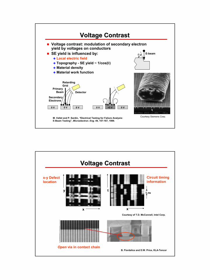
Voltage ContrastVoltage ContrastVoltage contrast: modulation of secondary electron yield by voltages on conductorsSE yield is influenced by:
Local electric fieldTopography - SE yield ~ 1/cos(θ)Material density Material work function
M. Vallet and P. Sardin, “Electrical Testing for Failure Analysis:E-Beam Testing”, Microelectron. Eng. 49, 157-167, 1999.
0 V 0 V 0 V
Detector
Retarding Grid
Primary Beam
SecondaryElectrons
0 V +5 V 0 V
Courtesy Siemens Corp.
E-beamθ
Voltage ContrastVoltage Contrast
Courtesy of T.D. McConnell, Intel Corp.
x
y
x
t1 ns
Open via in contact chainB. Fiordalice and D.W. Price, KLA-Tencor
x-y Defect location
Circuit timinginformation
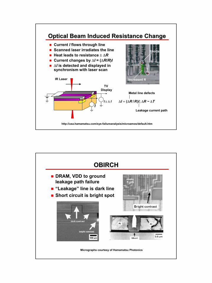
Optical Beam Induced Resistance ChangeOptical Beam Induced Resistance Change
IR Laser
TV Display
I ± ∆ II
Current I flows through lineScanned laser irradiates the lineHeat leads to resistance ± ∆RCurrent changes by ∆I = (∆R/R)I∆I is detected and displayed in synchronism with laser scan
Increased R
Shorts
TRIRRI ∆∆∆=∆ ~;)/(
Leakage current path
Metal line defects
http://usa.hamamatsu.com/sys-failureanalysis/microamos/default.htm
OBIRCHOBIRCHDRAM, VDD to ground leakage path failure“Leakage” line is dark lineShort circuit is bright spot
5 µm
Micrographs courtesy of Hamamatsu Photonics
Probe DiameterProbe Diameter
1 10 100 1,000Å 1 10 100µm 1mm 1cm
Analytical Diameter
Electrons
Ions
X-Rays
Light
Probes
Physical Failure Analysis ChallengesPhysical Failure Analysis ChallengesReduced feature sizeSmaller defects
Field - emission SEMTransmission electron microscopyConfocal microscopyScanning probe microscopy
New materials – new failure mechanisms?Al ⇒ CuSiO2 ⇒ low KSiO2 ⇒ high K
Single dislocation
NaImages courtesy of T.J. Shaffner, NIST
GateDrain
Depletion region Substrate
Source

Imaging of Single Bi Atoms in SiImaging of Single Bi Atoms in Si
EELS Spectrometer
EELS Spectrometer
E BeamE BeamScanning Scanning
ProbeProbe
The best TEM has resolution of 0.8 ÅCan see individual impurity atoms
Courtesy of G. Duscher, North Carolina State University
Bi
Z=31 Z=33
Conductive Atomic Force MicroscopyConductive Atomic Force Microscopy
Image courtesy A. Olbrich, Infineon
AFM Topograph Tunnel current image, 1 µm scan, 0.5 pA
current scale
Field GateOxides
C-AFM measures sample topography and currentAllows current-voltage measurements
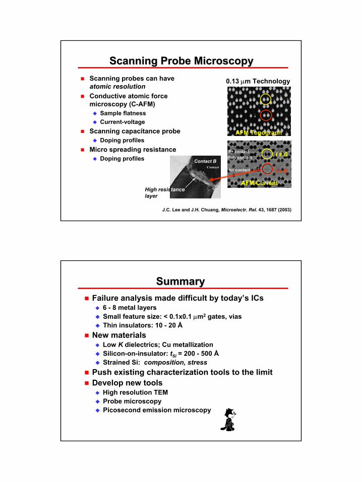
Scanning Probe MicroscopyScanning Probe MicroscopyScanning probes can have atomic resolutionConductive atomic force microscopy (C-AFM)
Sample flatnessCurrent-voltage
Scanning capacitance probeDoping profiles
Micro spreading resistanceDoping profiles
J.C. Lee and J.H. Chuang, Microelectr. Rel. 43, 1687 (2003)
AFM Topograph
AFM Current
Contact B
0.13 µm Technology
I ≠ 0
I = 0
High resistancelayer
Failure analysis made difficult by today’s ICs6 - 8 metal layersSmall feature size: < 0.1x0.1 µm2 gates, viasThin insulators: 10 - 20 Å
New materialsLow K dielectrics; Cu metallizationSilicon-on-insulator: tSi = 200 - 500 ÅStrained Si: composition, stress
Push existing characterization tools to the limitDevelop new tools
High resolution TEMProbe microscopy Picosecond emission microscopy
SummarySummary