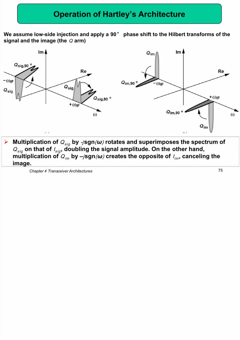
chapter4 transceiver architectures
TRANSCRIPT
8/12/2019 Chapter4 Transceiver Architectures
http://slidepdf.com/reader/full/chapter4-transceiver-architectures 1/137
1
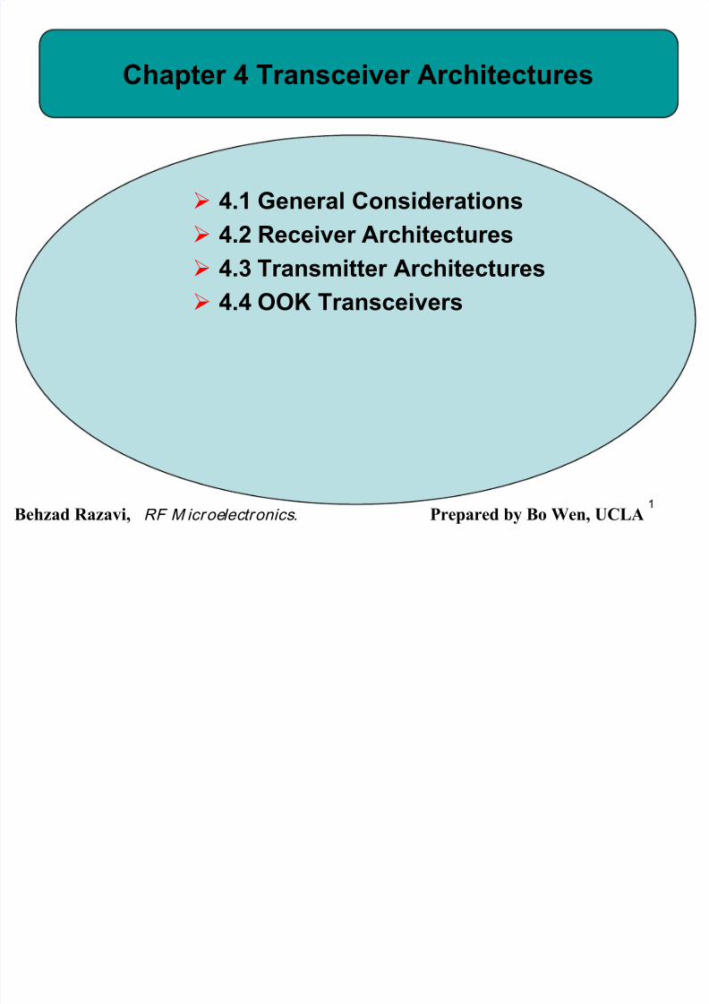
Chapter 4 Transceiver Architectures
4.1 General Considerations
4.2 Receiver Architectures
4.3 Transmitter Architectures
4.4 OOK Transceivers
Behzad Razavi, RF M icroelectronics. Prepared by Bo Wen, UCLA
8/12/2019 Chapter4 Transceiver Architectures
http://slidepdf.com/reader/full/chapter4-transceiver-architectures 2/137
Chapter 4 Transceiver Architectures 2
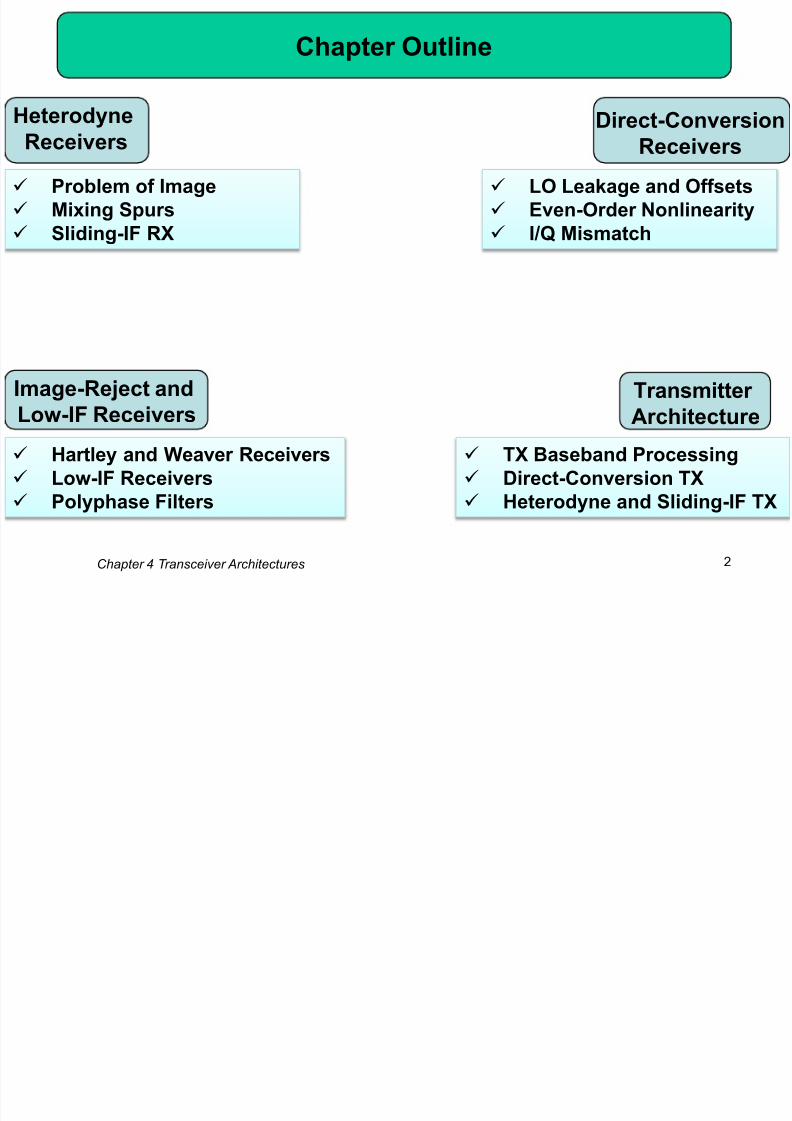
Chapter Outline
Heterodyne
Receivers
Image-Reject and
Low-IF Receivers
Problem of Image
Mixing Spurs
Sliding-IF RX
Transmitter
Architecture
LO Leakage and Offsets
Even-Order Nonlinearity
I/Q Mismatch
Hartley and Weaver Receivers
Low-IF Receivers
Polyphase Filters
TX Baseband Processing
Direct-Conversion TX
Heterodyne and Sliding-IF TX
Direct-Conversion
Receivers
8/12/2019 Chapter4 Transceiver Architectures
http://slidepdf.com/reader/full/chapter4-transceiver-architectures 3/137
Chapter 4 Transceiver Architectures 3
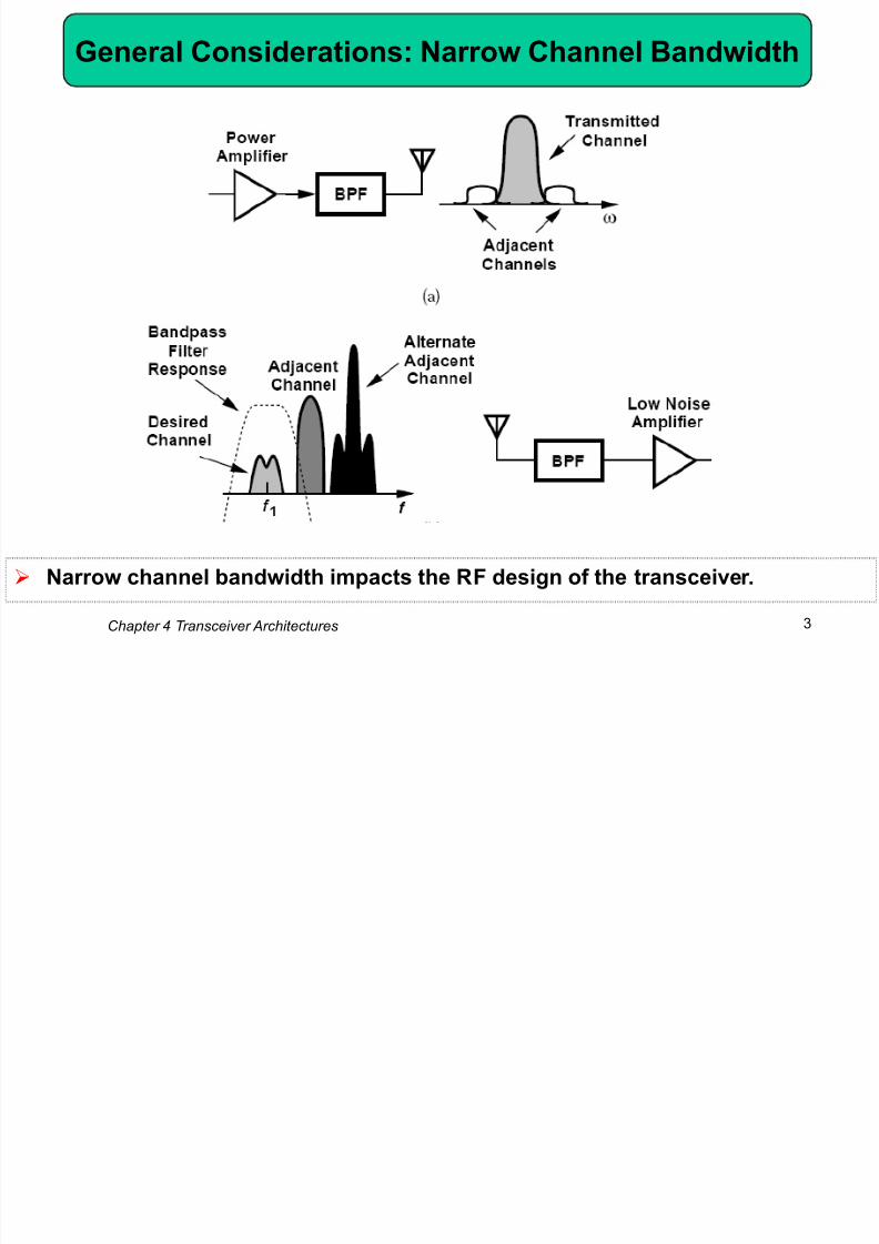
General Considerations: Narrow Channel Bandwidth
Narrow channel bandwidth impacts the RF design of the transceiver.

8/12/2019 Chapter4 Transceiver Architectures
http://slidepdf.com/reader/full/chapter4-transceiver-architectures 4/137
Chapter 4 Transceiver Architectures 4
Can We Simply Filter the Interferers to Relax the
Receiver Linearity Requirement?
First, the filter must provide a very high Q
Second, the filter would need a variable, yet precise center frequency
8/12/2019 Chapter4 Transceiver Architectures
http://slidepdf.com/reader/full/chapter4-transceiver-architectures 5/137
Chapter 4 Transceiver Architectures 5
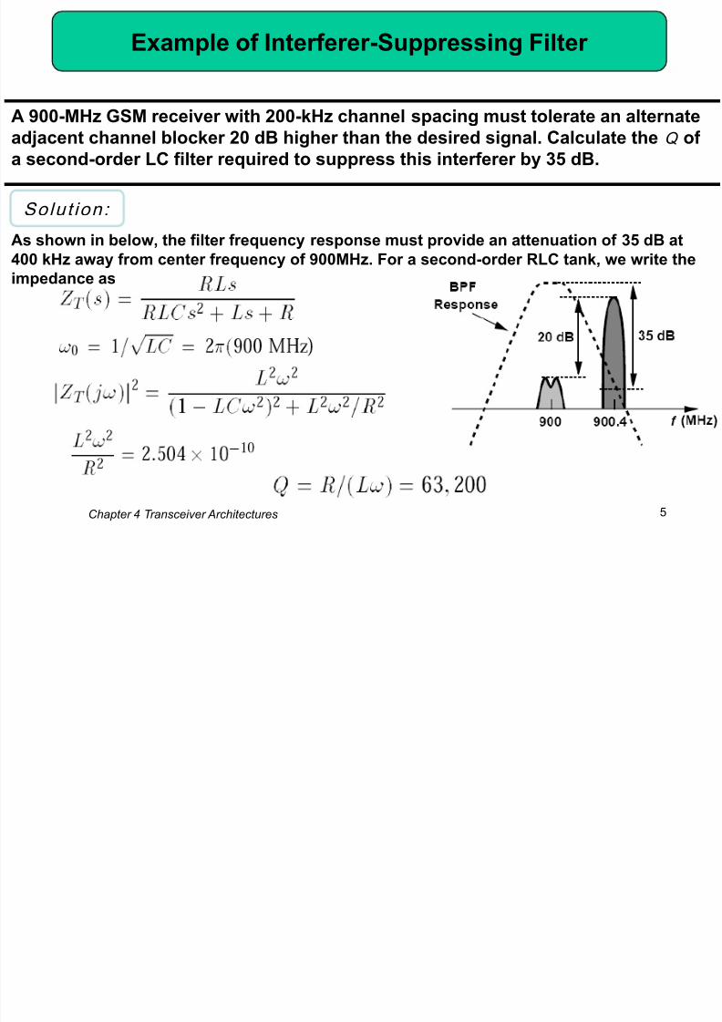
Example of Interferer-Suppressing Filter
Solut ion:
A 900-MHz GSM receiver with 200-kHz channel spacing must tolerate an alternateadjacent channel blocker 20 dB higher than the desired signal. Calculate the Q of
a second-order LC filter required to suppress this interferer by 35 dB.
As shown in below, the filter frequency response must provide an attenuation of 35 dB at
400 kHz away from center frequency of 900MHz. For a second-order RLC tank, we write the
impedance as

8/12/2019 Chapter4 Transceiver Architectures
http://slidepdf.com/reader/full/chapter4-transceiver-architectures 6/137
Chapter 4 Transceiver Architectures 6
Channel Selection and Band Selection
All of the stages in the receiver chain that precede channel-selection filtering
must be sufficiently linear
Channel selection must be deferred to some other point where centerfrequency is lower and hence required Q is more reasonable
Most receiver front ends do incorporate a ―band-select‖ filter
8/12/2019 Chapter4 Transceiver Architectures
http://slidepdf.com/reader/full/chapter4-transceiver-architectures 7/137
Chapter 4 Transceiver Architectures 7
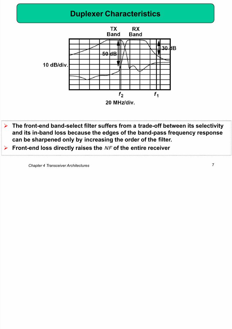
Duplexer Characteristics
The front-end band-select filter suffers from a trade-off between its selectivity
and its in-band loss because the edges of the band-pass frequency response
can be sharpened only by increasing the order of the filter.
Front-end loss directly raises the NF of the entire receiver
8/12/2019 Chapter4 Transceiver Architectures
http://slidepdf.com/reader/full/chapter4-transceiver-architectures 8/137
Chapter 4 Transceiver Architectures 8
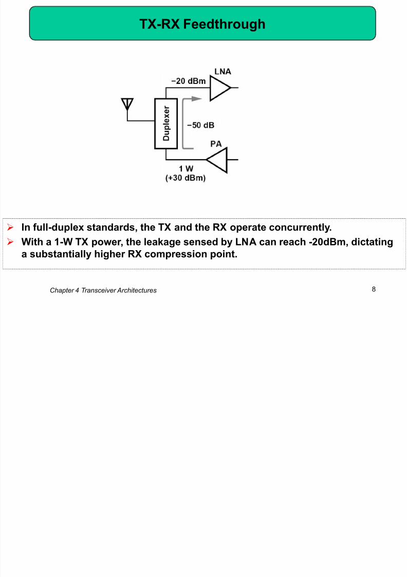
TX-RX Feedthrough
In full-duplex standards, the TX and the RX operate concurrently.
With a 1-W TX power, the leakage sensed by LNA can reach -20dBm, dictating
a substantially higher RX compression point.
8/12/2019 Chapter4 Transceiver Architectures
http://slidepdf.com/reader/full/chapter4-transceiver-architectures 9/137
Chapter 4 Transceiver Architectures 9
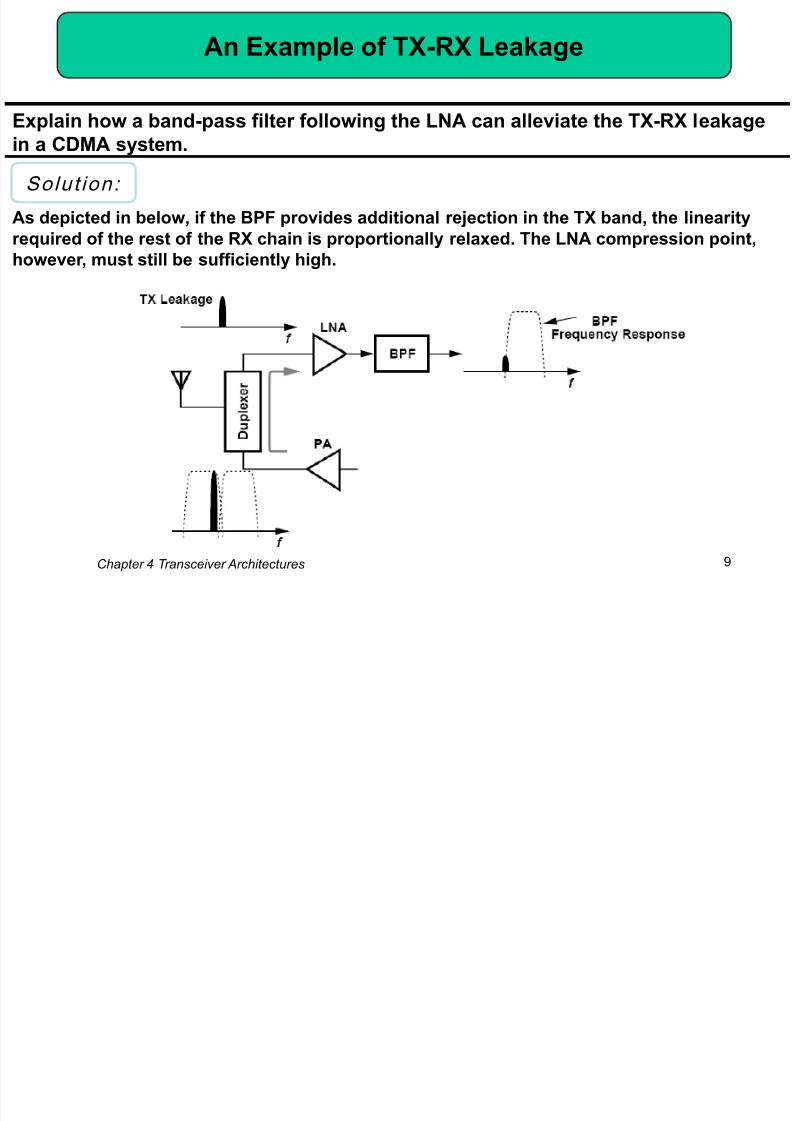
An Example of TX-RX Leakage
Solut ion:
Explain how a band-pass filter following the LNA can alleviate the TX-RX leakage
in a CDMA system.
As depicted in below, if the BPF provides additional rejection in the TX band, the linearity
required of the rest of the RX chain is proportionally relaxed. The LNA compression point,
however, must still be sufficiently high.
8/12/2019 Chapter4 Transceiver Architectures
http://slidepdf.com/reader/full/chapter4-transceiver-architectures 10/137
Chapter 4 Transceiver Architectures 10
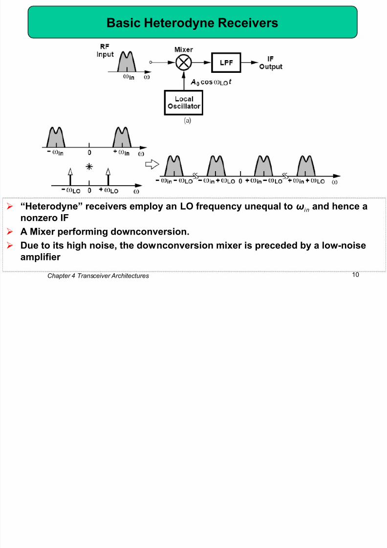
Basic Heterodyne Receivers
―Heterodyne‖ receivers employ an LO frequency unequal to ωin and hence a
nonzero IF
A Mixer performing downconversion.
Due to its high noise, the downconversion mixer is preceded by a low-noise
amplifier

8/12/2019 Chapter4 Transceiver Architectures
http://slidepdf.com/reader/full/chapter4-transceiver-architectures 11/137
Chapter 4 Transceiver Architectures 11
Constant LO: each RF channel is downconverted to a different IF channel
How Does a Heterodyne Receiver Cover a Given
Frequency Band?
Constant IF: LO frequency is variable, all RF channels within the band of
interest translated to a single value of IF.
8/12/2019 Chapter4 Transceiver Architectures
http://slidepdf.com/reader/full/chapter4-transceiver-architectures 12/137
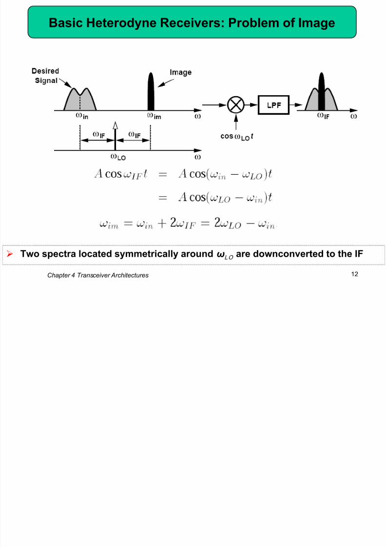
Chapter 4 Transceiver Architectures 12
Basic Heterodyne Receivers: Problem of Image
Two spectra located symmetrically around ωLO are downconverted to the IF
8/12/2019 Chapter4 Transceiver Architectures
http://slidepdf.com/reader/full/chapter4-transceiver-architectures 13/137
Chapter 4 Transceiver Architectures 13
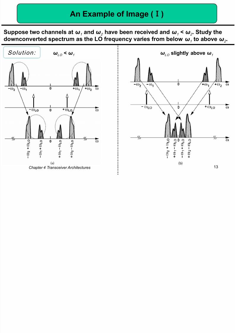
An Example of Image ( )
Solut ion:
Suppose two channels at ω1 and ω2 have been received and ω1 < ω2 . Study the
downconverted spectrum as the LO frequency varies from below ω1 to above ω2 .
ωLO < ω1 ωLO slightly above ω1

8/12/2019 Chapter4 Transceiver Architectures
http://slidepdf.com/reader/full/chapter4-transceiver-architectures 14/137
Chapter 4 Transceiver Architectures 14
Solut ion:
An Example of Image ( )
Suppose two channels at ω1 and ω2 have been received and ω1 < ω2 . Study the
downconverted spectrum as the LO frequency varies from below ω1 to above ω2 .
ωLO midway between ω1 and ω2 ωLO > ω2

8/12/2019 Chapter4 Transceiver Architectures
http://slidepdf.com/reader/full/chapter4-transceiver-architectures 15/137
Chapter 4 Transceiver Architectures 15
Another Example of Image
Solut ion:
Formulate the downconversion above using expressions for the desired signal
and the image.
and
We observe that the components at ωin + ωLO and ωim + ωLO are removed by low-pass filtering,
and those at ωin - ωLO = - ωIF and ωim - ωLO = + ωIF coincide.

8/12/2019 Chapter4 Transceiver Architectures
http://slidepdf.com/reader/full/chapter4-transceiver-architectures 16/137
Chapter 4 Transceiver Architectures 16
An Example of High-Side and Low-Side Injection
Solut ion:
The designer of an IEEE802.11g receiver attempts to place the image frequency in
the GPS band, which contains only low-level satellite transmissions and hence nostrong interferers. Is this possible?
The two bands are shown below. The LO frequency must cover a range of 80MHz but,
unfortunately, the GPS band spans only 20 MHz. For example, if the lowest LO frequency ischosen so as to make 1.565 GHz the image of 2.4 GHz, then 802.11g channels above 2.42
GHz have images beyond the GPS band.
8/12/2019 Chapter4 Transceiver Architectures
http://slidepdf.com/reader/full/chapter4-transceiver-architectures 17/137
Chapter 4 Transceiver Architectures 17
Another Example of High-Side and Low-Side
Injection
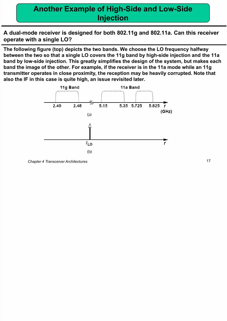
A dual-mode receiver is designed for both 802.11g and 802.11a. Can this receiver
operate with a single LO?
The following figure (top) depicts the two bands. We choose the LO frequency halfway
between the two so that a single LO covers the 11g band by high-side injection and the 11a
band by low-side injection. This greatly simplifies the design of the system, but makes each
band the image of the other. For example, if the receiver is in the 11a mode while an 11g
transmitter operates in close proximity, the reception may be heavily corrupted. Note that
also the IF in this case is quite high, an issue revisited later.
8/12/2019 Chapter4 Transceiver Architectures
http://slidepdf.com/reader/full/chapter4-transceiver-architectures 18/137
Chapter 4 Transceiver Architectures 18
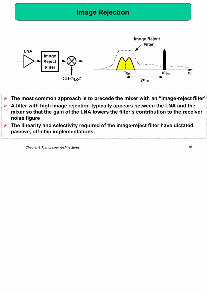
The most common approach is to precede the mixer with an ―image-reject filter‖
A filter with high image rejection typically appears between the LNA and the
mixer so that the gain of the LNA lowers the filter’s contribution to the receiver
noise figure
The linearity and selectivity required of the image-reject filter have dictated
passive, off-chip implementations.
Image Rejection
8/12/2019 Chapter4 Transceiver Architectures
http://slidepdf.com/reader/full/chapter4-transceiver-architectures 19/137
Chapter 4 Transceiver Architectures 19
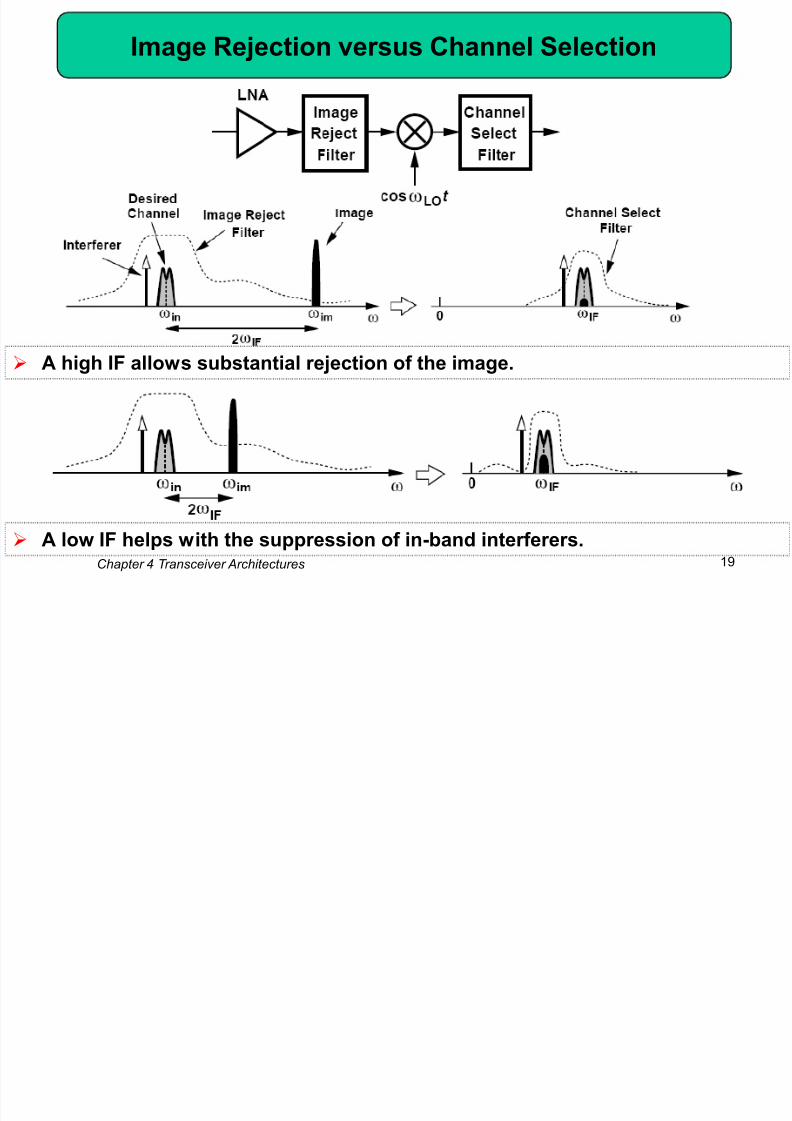
A high IF allows substantial rejection of the image.
Image Rejection versus Channel Selection
A low IF helps with the suppression of in-band interferers.
8/12/2019 Chapter4 Transceiver Architectures
http://slidepdf.com/reader/full/chapter4-transceiver-architectures 20/137
Chapter 4 Transceiver Architectures 20
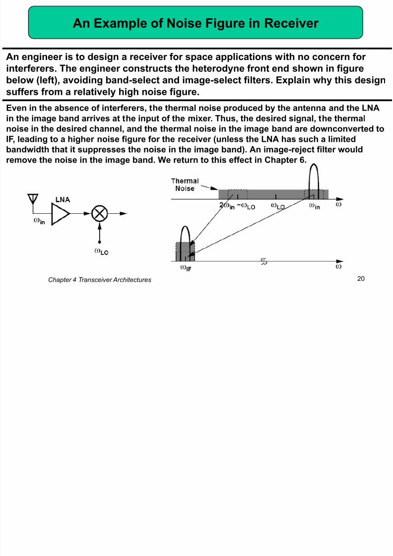
An Example of Noise Figure in Receiver
An engineer is to design a receiver for space applications with no concern for
interferers. The engineer constructs the heterodyne front end shown in figurebelow (left), avoiding band-select and image-select filters. Explain why this design
suffers from a relatively high noise figure.
Even in the absence of interferers, the thermal noise produced by the antenna and the LNA
in the image band arrives at the input of the mixer. Thus, the desired signal, the thermal
noise in the desired channel, and the thermal noise in the image band are downconverted to
IF, leading to a higher noise figure for the receiver (unless the LNA has such a limitedbandwidth that it suppresses the noise in the image band). An image-reject filter would
remove the noise in the image band. We return to this effect in Chapter 6.
8/12/2019 Chapter4 Transceiver Architectures
http://slidepdf.com/reader/full/chapter4-transceiver-architectures 21/137
Chapter 4 Transceiver Architectures 21
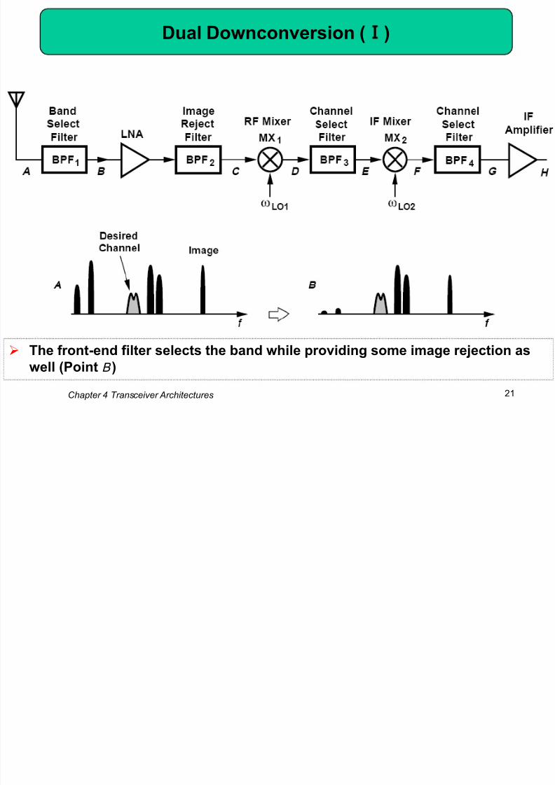
Dual Downconversion ( )
The front-end filter selects the band while providing some image rejection as
well (Point B )
8/12/2019 Chapter4 Transceiver Architectures
http://slidepdf.com/reader/full/chapter4-transceiver-architectures 22/137
Chapter 4 Transceiver Architectures 22
Dual Downconversion ( )
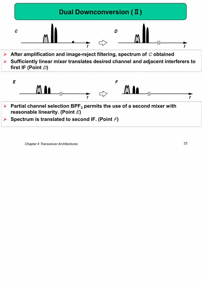
After amplification and image-reject filtering, spectrum of C obtained
Sufficiently linear mixer translates desired channel and adjacent interferers to
first IF (Point D )
Partial channel selection BPF3 permits the use of a second mixer withreasonable linearity. (Point E )
Spectrum is translated to second IF. (Point F )
8/12/2019 Chapter4 Transceiver Architectures
http://slidepdf.com/reader/full/chapter4-transceiver-architectures 23/137
Chapter 4 Transceiver Architectures 23
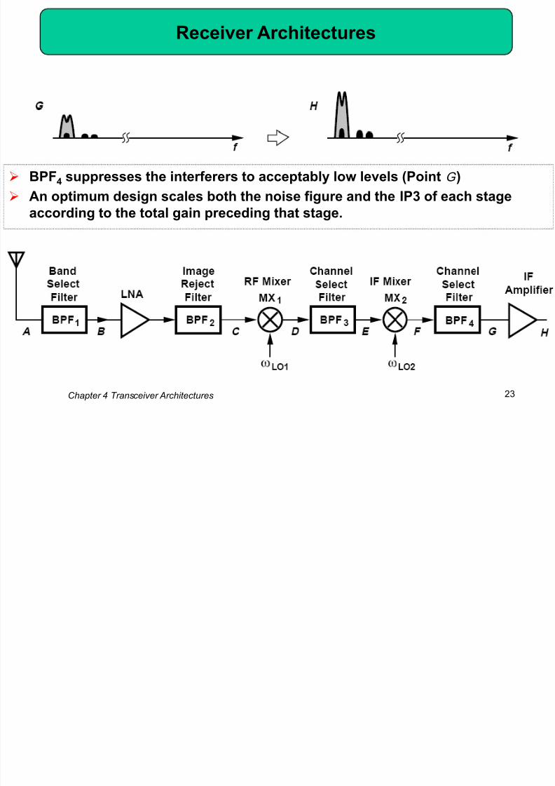
Receiver Architectures
BPF4 suppresses the interferers to acceptably low levels (Point G )
An optimum design scales both the noise figure and the IP3 of each stageaccording to the total gain preceding that stage.

8/12/2019 Chapter4 Transceiver Architectures
http://slidepdf.com/reader/full/chapter4-transceiver-architectures 24/137
Chapter 4 Transceiver Architectures 24
Another Example of Image
Solut ion:
Assuming low-side injection for both downconversion mixers in figure above,
determine the image frequencies.
As shown below, the first image lies at 2ωLO1 - ωin . The second image is located at 2ωLO2 -
(ωin - ωLO1 ).
8/12/2019 Chapter4 Transceiver Architectures
http://slidepdf.com/reader/full/chapter4-transceiver-architectures 25/137
Chapter 4 Transceiver Architectures 25
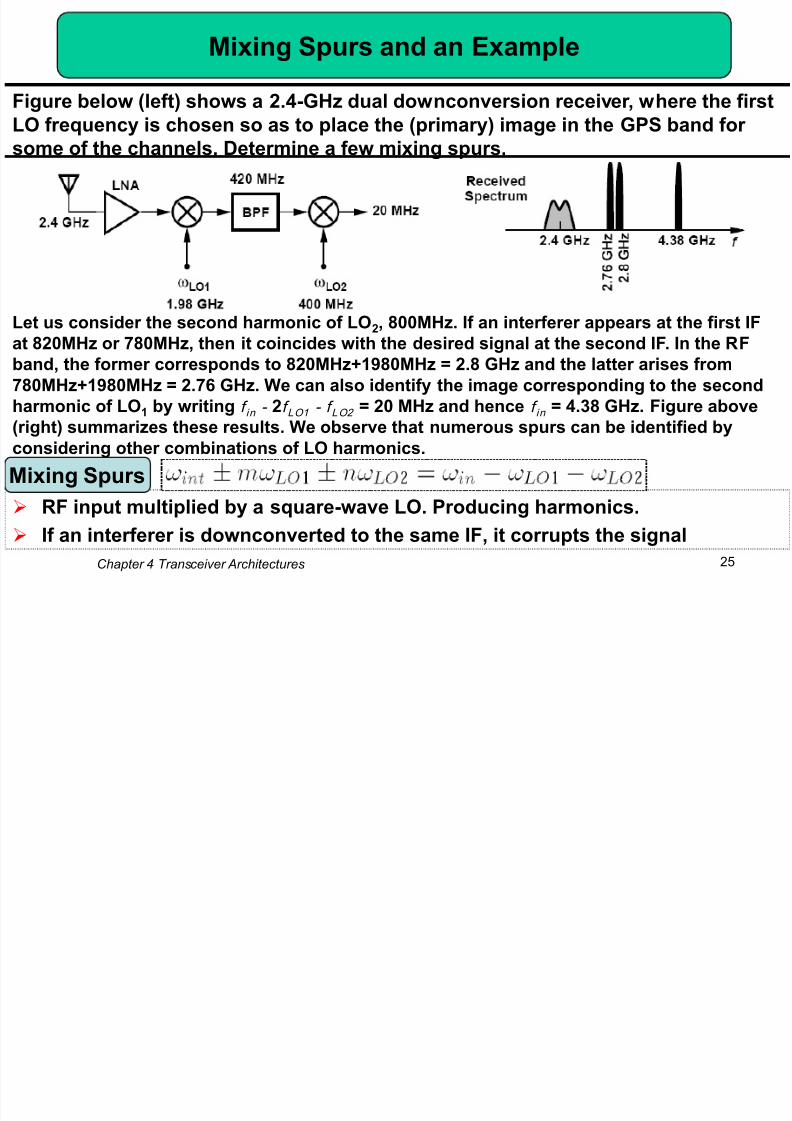
Mixing Spurs and an Example
RF input multiplied by a square-wave LO. Producing harmonics.
If an interferer is downconverted to the same IF, it corrupts the signal
Mixing Spurs
Figure below (left) shows a 2.4-GHz dual downconversion receiver, where the first
LO frequency is chosen so as to place the (primary) image in the GPS band for
some of the channels. Determine a few mixing spurs.
Let us consider the second harmonic of LO2, 800MHz. If an interferer appears at the first IF
at 820MHz or 780MHz, then it coincides with the desired signal at the second IF. In the RF
band, the former corresponds to 820MHz+1980MHz = 2.8 GHz and the latter arises from
780MHz+1980MHz = 2.76 GHz. We can also identify the image corresponding to the second
harmonic of LO1
by writing f in
- 2f LO1
- f LO2
= 20 MHz and hence f in
= 4.38 GHz. Figure above
(right) summarizes these results. We observe that numerous spurs can be identified by
considering other combinations of LO harmonics.

8/12/2019 Chapter4 Transceiver Architectures
http://slidepdf.com/reader/full/chapter4-transceiver-architectures 26/137
Chapter 4 Transceiver Architectures 26
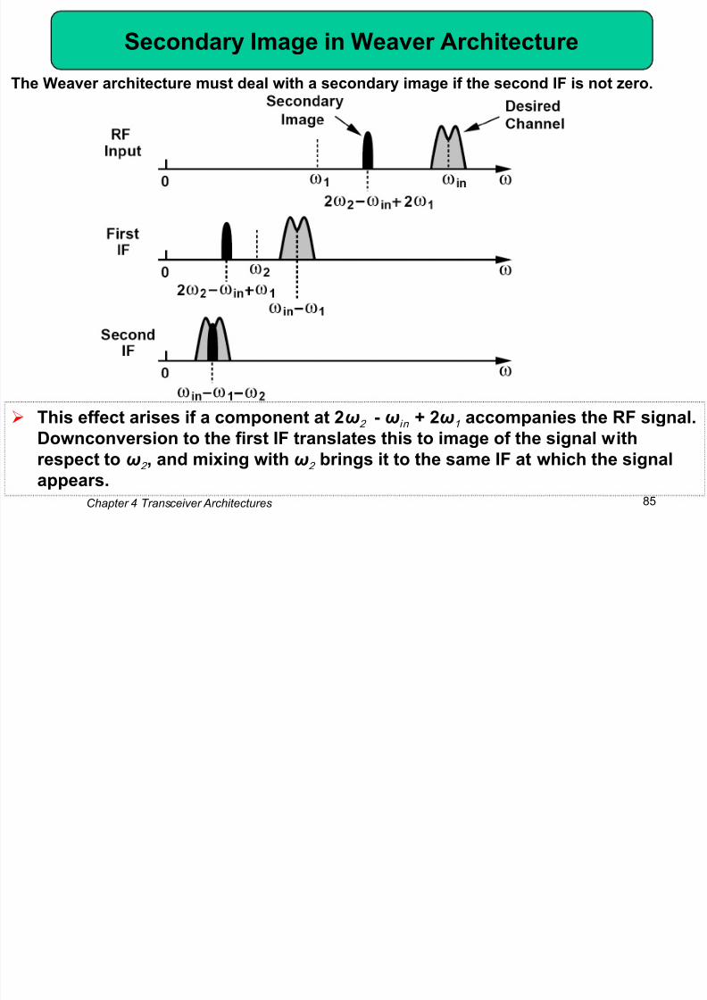
Zero Second IF
To avoid secondary image, most modern heterodyne receivers employ a zero
second IF. In this case, the image is the signal itself. No interferer at other frequencies
can be downconverted as an image to a zero center frequency if ωLO2 =ωIF1
8/12/2019 Chapter4 Transceiver Architectures
http://slidepdf.com/reader/full/chapter4-transceiver-architectures 27/137
Chapter 4 Transceiver Architectures 27
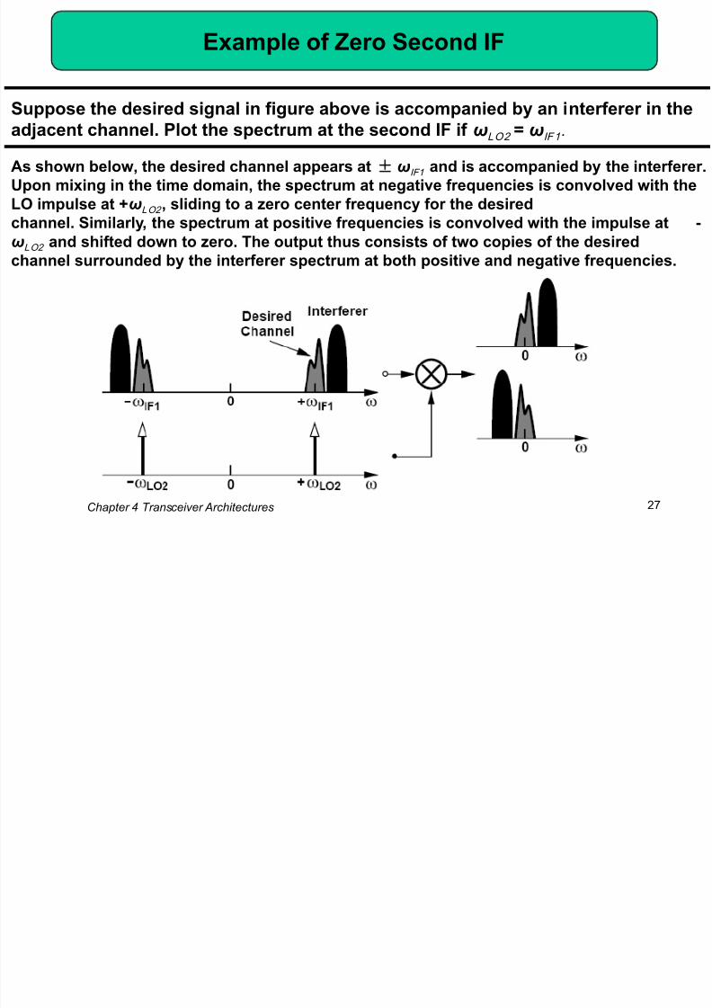
Example of Zero Second IF
Suppose the desired signal in figure above is accompanied by an interferer in the
adjacent channel. Plot the spectrum at the second IF if ωLO2 = ωIF1 .
As shown below, the desired channel appears at ωIF1 and is accompanied by the interferer.
Upon mixing in the time domain, the spectrum at negative frequencies is convolved with the
LO impulse at +ωLO2 , sliding to a zero center frequency for the desired
channel. Similarly, the spectrum at positive frequencies is convolved with the impulse at -
ωLO2
and shifted down to zero. The output thus consists of two copies of the desired
channel surrounded by the interferer spectrum at both positive and negative frequencies.

8/12/2019 Chapter4 Transceiver Architectures
http://slidepdf.com/reader/full/chapter4-transceiver-architectures 28/137
Chapter 4 Transceiver Architectures 28
Symmetrically-modulated versus Asymmetrically-
modulated Signal
AM signals are symmetric, FM signals are asymmetric. Most of today’s modulation schemes, e.g., FSK, QPSK, GMSK, and QAM,
exhibit asymmetric spectra around carrier frequency.
AM signal generation FM signal generation
8/12/2019 Chapter4 Transceiver Architectures
http://slidepdf.com/reader/full/chapter4-transceiver-architectures 29/137
Chapter 4 Transceiver Architectures 29
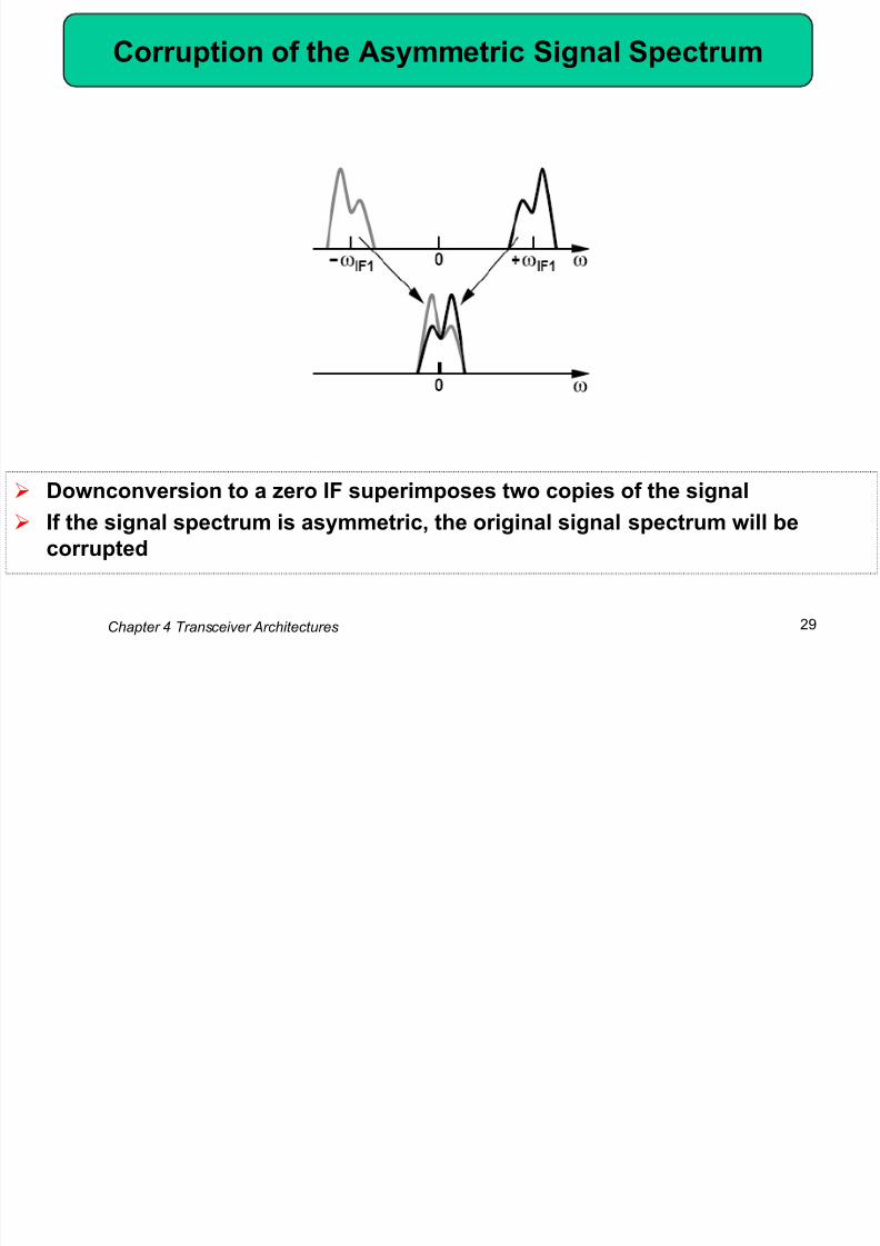
Corruption of the Asymmetric Signal Spectrum
Downconversion to a zero IF superimposes two copies of the signal
If the signal spectrum is asymmetric, the original signal spectrum will be
corrupted

8/12/2019 Chapter4 Transceiver Architectures
http://slidepdf.com/reader/full/chapter4-transceiver-architectures 30/137
Chapter 4 Transceiver Architectures 30
An Example of Self-corruption
Solut ion:
Downconversion to what minimum intermediate frequency avoids self-corruptionof asymmetric signals?
To avoid self-corruption, the downconverted spectra must not overlap each other. Thus, as
shown in figure below, the signal can be downconverted to an IF equal to half of the signal
bandwidth. Of course, an interferer may now become the image.
f
8/12/2019 Chapter4 Transceiver Architectures
http://slidepdf.com/reader/full/chapter4-transceiver-architectures 31/137
Chapter 4 Transceiver Architectures 31
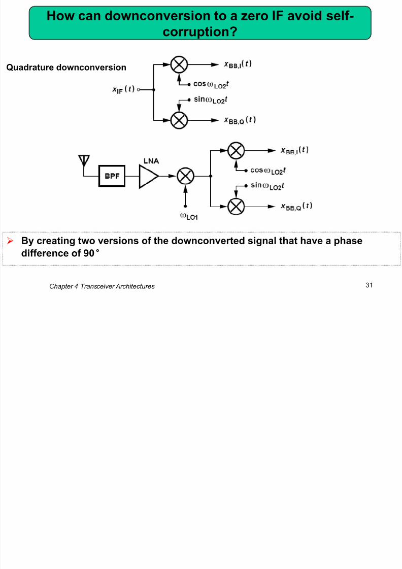
How can downconversion to a zero IF avoid self-
corruption?
By creating two versions of the downconverted signal that have a phase
difference of 90
Quadrature downconversion
8/12/2019 Chapter4 Transceiver Architectures
http://slidepdf.com/reader/full/chapter4-transceiver-architectures 32/137
Chapter 4 Transceiver Architectures 32
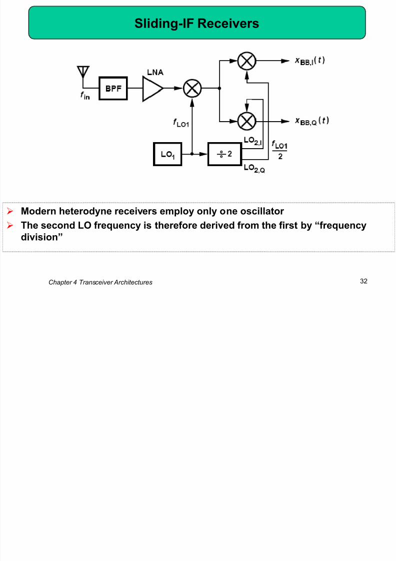
Sliding-IF Receivers
Modern heterodyne receivers employ only one oscillator
The second LO frequency is therefore derived from the first by ―frequency
division‖
8/12/2019 Chapter4 Transceiver Architectures
http://slidepdf.com/reader/full/chapter4-transceiver-architectures 33/137
Chapter 4 Transceiver Architectures 33
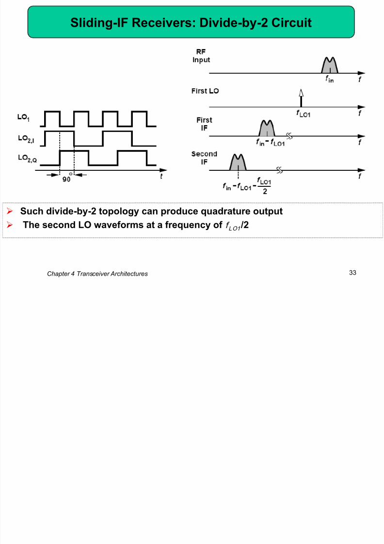
Sliding-IF Receivers: Divide-by-2 Circuit
Such divide-by-2 topology can produce quadrature output
The second LO waveforms at a frequency of f LO1 /2
8/12/2019 Chapter4 Transceiver Architectures
http://slidepdf.com/reader/full/chapter4-transceiver-architectures 34/137
Chapter 4 Transceiver Architectures 34
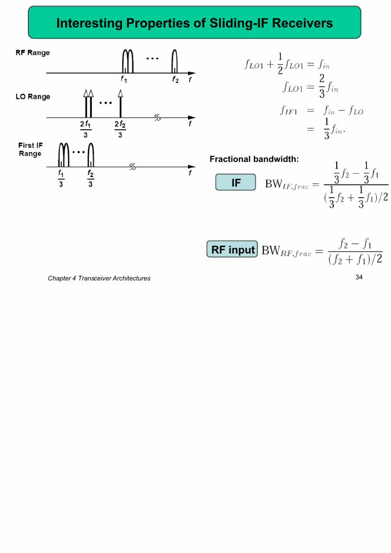
Interesting Properties of Sliding-IF Receivers
IF
RF input
Fractional bandwidth:

8/12/2019 Chapter4 Transceiver Architectures
http://slidepdf.com/reader/full/chapter4-transceiver-architectures 35/137
Chapter 4 Transceiver Architectures 35
An Example of Sliding-IF Receivers
Solut ion:
Suppose the input band is partitioned into N channels, each having a bandwidthof (f 2 - f 1 )/N = Δf . How does the LO frequency vary as the receiver translates each
channel to a zero second IF?
The first channel is located between f 1 and f 1 + Δf . Thus the first LO frequency is chosen
equal to two-third of the center of the channel: f LO = (2/3)(f 1 + Δf/ 2 ). Similarly, for the second
channel, located between f 1 + Δf and f 1 + 2 Δf , the LO frequency must be equal to (2/3)(f 1 +
3 Δf /2). In other words, the LO increments in steps of (2/3) Δ f .
8/12/2019 Chapter4 Transceiver Architectures
http://slidepdf.com/reader/full/chapter4-transceiver-architectures 36/137
Chapter 4 Transceiver Architectures 36
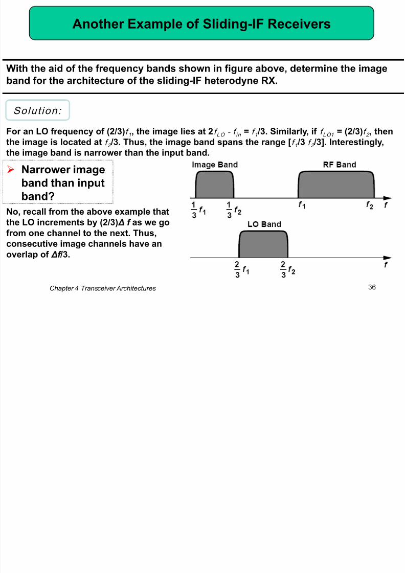
Another Example of Sliding-IF Receivers
Solut ion:
Narrower image
band than input
band?
With the aid of the frequency bands shown in figure above, determine the imageband for the architecture of the sliding-IF heterodyne RX.
For an LO frequency of (2/3)f 1 , the image lies at 2f LO - f in = f 1 /3. Similarly, if f LO1 = (2/3)f 2 , then
the image is located at f 2 /3. Thus, the image band spans the range [f 1 /3 f 2 /3]. Interestingly,the image band is narrower than the input band.
No, recall from the above example thatthe LO increments by (2/3) Δ f as we go
from one channel to the next. Thus,
consecutive image channels have an
overlap of Δf /3.

8/12/2019 Chapter4 Transceiver Architectures
http://slidepdf.com/reader/full/chapter4-transceiver-architectures 37/137
Chapter 4 Transceiver Architectures 37
Sliding-IF Receivers with Divide Ratio of 4
May incorporate greater divide ratios, e.g., 4
Second LO f in /5, slightly lower, desirable because generation of LO quadrature
phases at lower frequencies incurs smaller mismatches Reduces the frequency difference between the image and the signal, difficult to
reject image.
8/12/2019 Chapter4 Transceiver Architectures
http://slidepdf.com/reader/full/chapter4-transceiver-architectures 38/137
Chapter 4 Transceiver Architectures 38
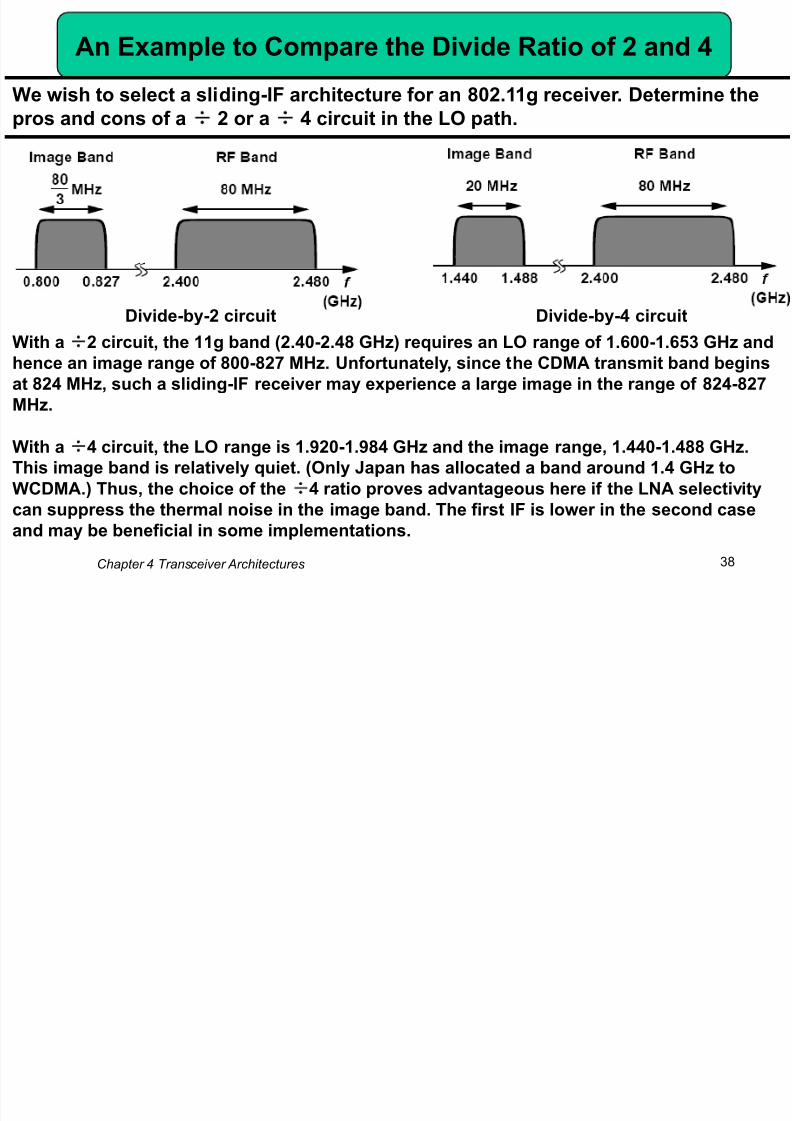
An Example to Compare the Divide Ratio of 2 and 4
We wish to select a sliding-IF architecture for an 802.11g receiver. Determine the
pros and cons of a÷ 2 or a÷ 4 circuit in the LO path.
With a÷2 circuit, the 11g band (2.40-2.48 GHz) requires an LO range of 1.600-1.653 GHz and
hence an image range of 800-827 MHz. Unfortunately, since the CDMA transmit band begins
at 824 MHz, such a sliding-IF receiver may experience a large image in the range of 824-827
MHz.
With a÷4 circuit, the LO range is 1.920-1.984 GHz and the image range, 1.440-1.488 GHz.
This image band is relatively quiet. (Only Japan has allocated a band around 1.4 GHz to
WCDMA.) Thus, the choice of the ÷4 ratio proves advantageous here if the LNA selectivity
can suppress the thermal noise in the image band. The first IF is lower in the second case
and may be beneficial in some implementations.
Divide-by-2 circuit Divide-by-4 circuit

8/12/2019 Chapter4 Transceiver Architectures
http://slidepdf.com/reader/full/chapter4-transceiver-architectures 39/137
Chapter 4 Transceiver Architectures 39
Direct-Conversion Receivers
Absence of an image greatly simplifies the design process
Channel selection is performed by on-chip low-pass filter
Mixing spurs are considerably reduced in number
8/12/2019 Chapter4 Transceiver Architectures
http://slidepdf.com/reader/full/chapter4-transceiver-architectures 40/137
Chapter 4 Transceiver Architectures 40
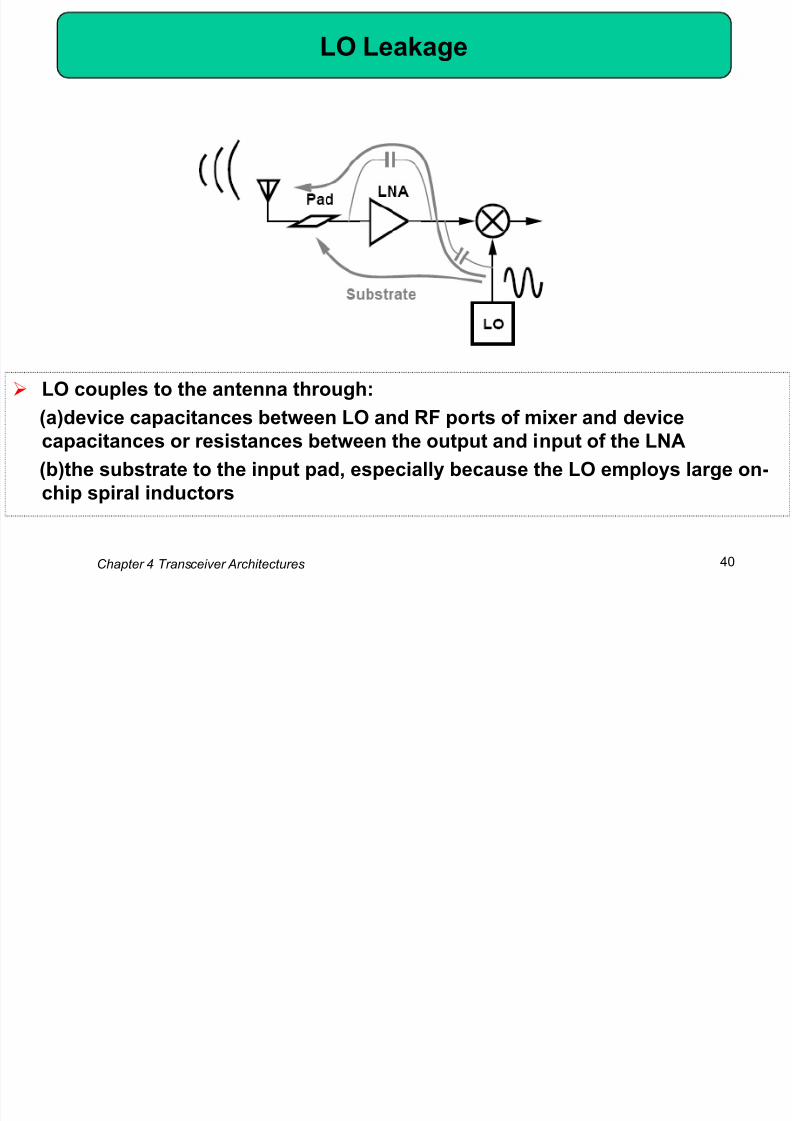
LO Leakage
LO couples to the antenna through:
(a)device capacitances between LO and RF ports of mixer and devicecapacitances or resistances between the output and input of the LNA
(b)the substrate to the input pad, especially because the LO employs large on-
chip spiral inductors

8/12/2019 Chapter4 Transceiver Architectures
http://slidepdf.com/reader/full/chapter4-transceiver-architectures 41/137
Chapter 4 Transceiver Architectures 41
An Example of LO Leakage
Solut ion:
Determine the LO leakage from the output to the input of a cascode LNA.
If g m2 >> 1/ r O2
8/12/2019 Chapter4 Transceiver Architectures
http://slidepdf.com/reader/full/chapter4-transceiver-architectures 42/137
Chapter 4 Transceiver Architectures 42
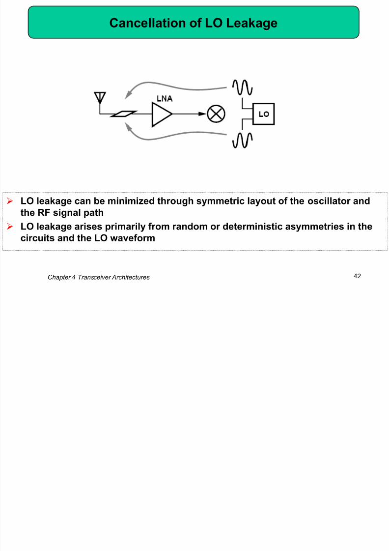
Cancellation of LO Leakage
LO leakage can be minimized through symmetric layout of the oscillator and
the RF signal path
LO leakage arises primarily from random or deterministic asymmetries in the
circuits and the LO waveform
8/12/2019 Chapter4 Transceiver Architectures
http://slidepdf.com/reader/full/chapter4-transceiver-architectures 43/137
Chapter 4 Transceiver Architectures 43
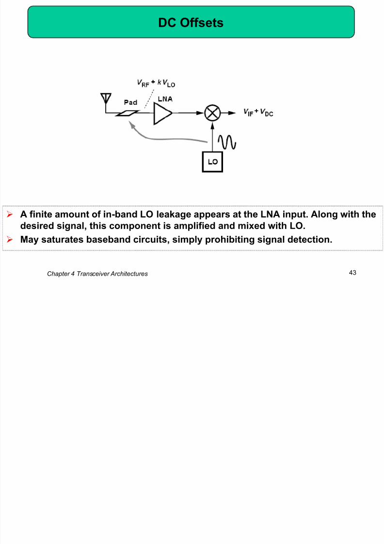
DC Offsets
A finite amount of in-band LO leakage appears at the LNA input. Along with the
desired signal, this component is amplified and mixed with LO.
May saturates baseband circuits, simply prohibiting signal detection.
8/12/2019 Chapter4 Transceiver Architectures
http://slidepdf.com/reader/full/chapter4-transceiver-architectures 44/137
Chapter 4 Transceiver Architectures 44
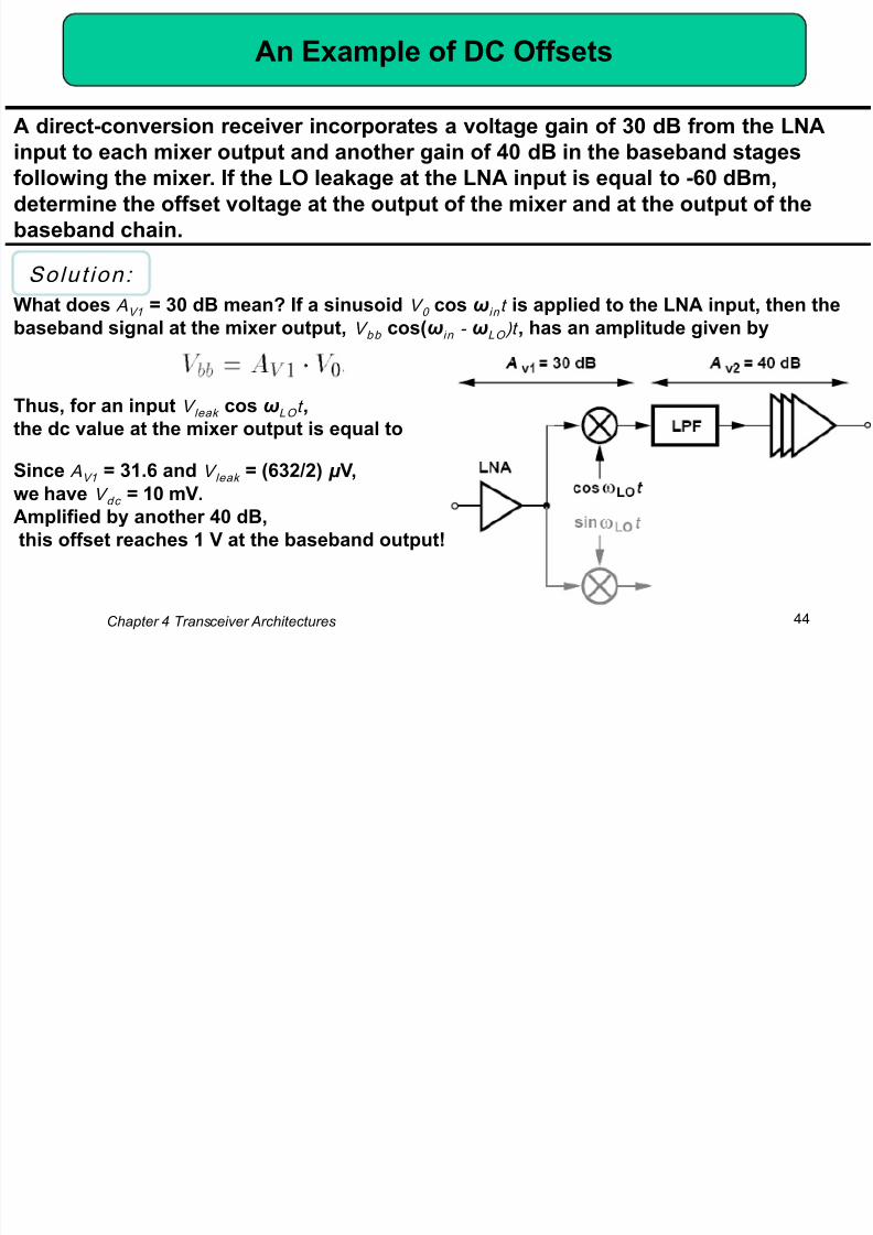
An Example of DC Offsets
Solut ion:
A direct-conversion receiver incorporates a voltage gain of 30 dB from the LNA
input to each mixer output and another gain of 40 dB in the baseband stagesfollowing the mixer. If the LO leakage at the LNA input is equal to -60 dBm,
determine the offset voltage at the output of the mixer and at the output of the
baseband chain.
What does AV1 = 30 dB mean? If a sinusoid V 0 cos ωin t is applied to the LNA input, then thebaseband signal at the mixer output, V bb cos(ωin - ωLO )t , has an amplitude given by
Thus, for an input V leak cos ωLO t ,
the dc value at the mixer output is equal to
Since AV1 = 31.6 and V leak = (632/2) μ V,
we have V dc = 10 mV.
Amplified by another 40 dB,
this offset reaches 1 V at the baseband output!

8/12/2019 Chapter4 Transceiver Architectures
http://slidepdf.com/reader/full/chapter4-transceiver-architectures 45/137
Chapter 4 Transceiver Architectures 45
Another Example of DC Offsets
Solut ion:
The dc offsets measured in the baseband I and Q outputs are often unequal.
Explain why
Suppose, in the presence of the quadrature phases of the LO, the net LO leakage at the
input of the LNA is expressed as V leak cos(ωLO t +Φ leak ), where Φ leak arises from the phase
shift through the path(s) from each LO phase to the LNA input and also the summation of
the leakages V LO cos ωLO t and VLO sinωLO t . The LO leakage travels through the LNA and
each mixer, experiencing an additional phase shift, Φ ckt , and is multiplied by V LO cos ωLO t
and V LO sin ωLO t . The dc components are therefore given by Thus, the two dc offsets are
generally unequal.
8/12/2019 Chapter4 Transceiver Architectures
http://slidepdf.com/reader/full/chapter4-transceiver-architectures 46/137
Chapter 4 Transceiver Architectures 46
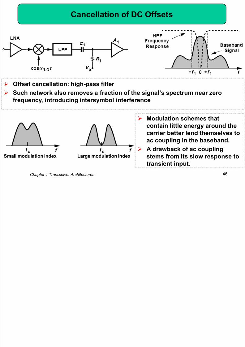
Cancellation of DC Offsets
Offset cancellation: high-pass filter
Such network also removes a fraction of the signal’s spectrum near zero
frequency, introducing intersymbol interference
Modulation schemes that
contain little energy around the
carrier better lend themselves to
ac coupling in the baseband.
A drawback of ac coupling
stems from its slow response to
transient input.
Small modulation index Large modulation index
8/12/2019 Chapter4 Transceiver Architectures
http://slidepdf.com/reader/full/chapter4-transceiver-architectures 47/137
Chapter 4 Transceiver Architectures 47
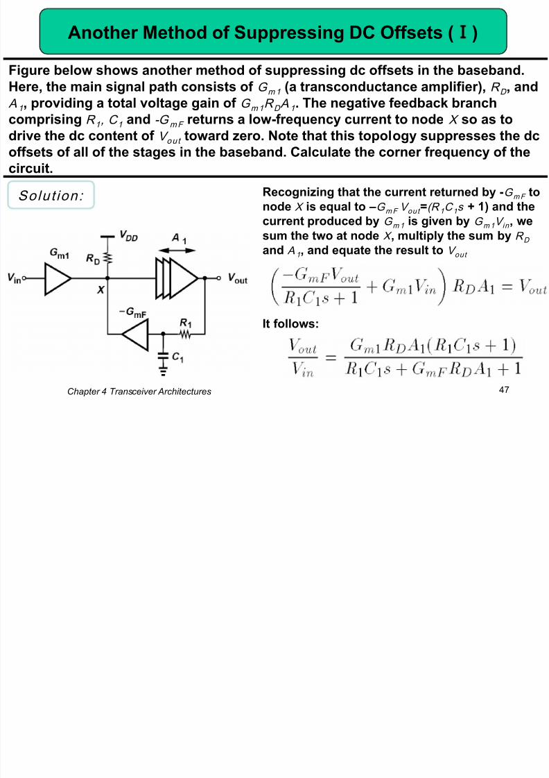
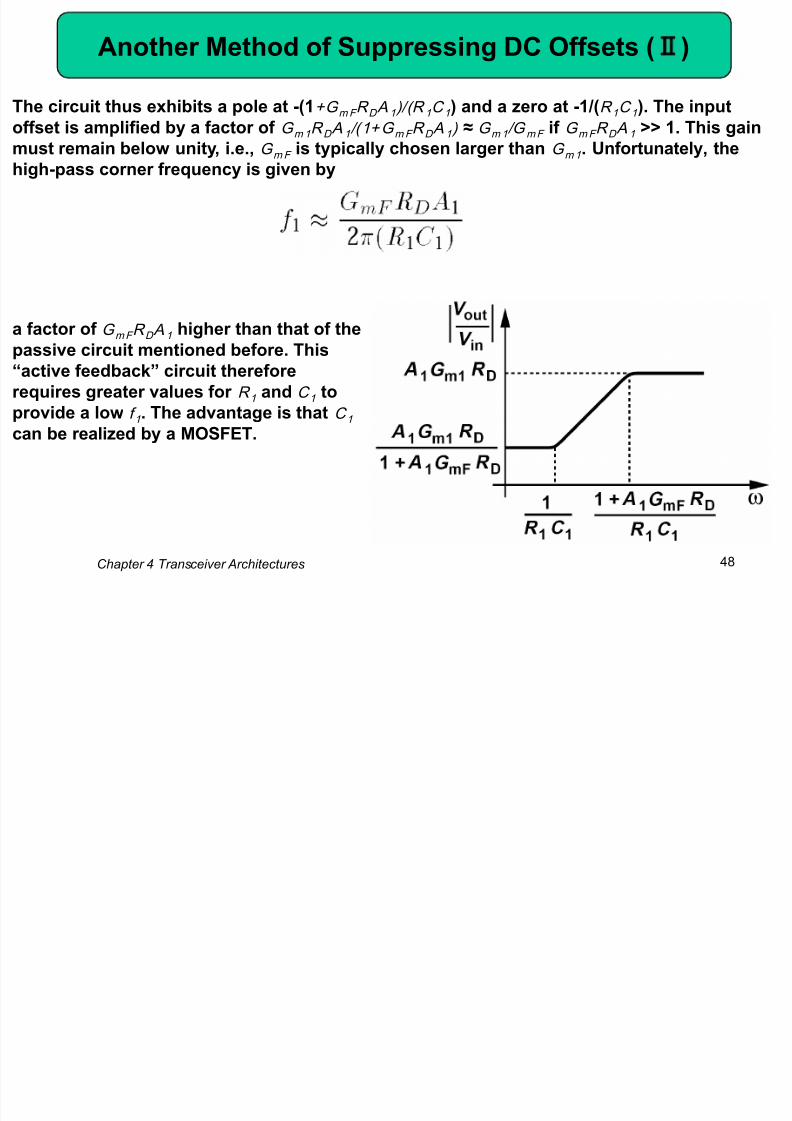
Another Method of Suppressing DC Offsets ( )
Figure below shows another method of suppressing dc offsets in the baseband.
Here, the main signal path consists of G m1 (a transconductance amplifier), R D , and
A 1 , providing a total voltage gain of G m1 R D A 1 . The negative feedback branchcomprising R 1 , C 1 and -G mF returns a low-frequency current to node X so as to
drive the dc content of V out toward zero. Note that this topology suppresses the dc
offsets of all of the stages in the baseband. Calculate the corner frequency of the
circuit.
Recognizing that the current returned by -G mF tonode X is equal to –G mF V out =(R 1 C 1 s + 1) and the
current produced by G m1 is given by G m1 V in , we
sum the two at node X , multiply the sum by R D
and A 1 , and equate the result to V out
It follows:
Solut ion:
8/12/2019 Chapter4 Transceiver Architectures
http://slidepdf.com/reader/full/chapter4-transceiver-architectures 48/137
Chapter 4 Transceiver Architectures 48
Another Method of Suppressing DC Offsets ( )
The circuit thus exhibits a pole at -(1+G mF R D A 1 )/(R 1 C 1 ) and a zero at -1/(R 1 C 1 ). The input
offset is amplified by a factor of G m1 R D A 1 /(1+G mF R D A 1 ) ≈ G m1 /G mF if G mF R D A 1 >> 1. This gain
must remain below unity, i.e., G mF is typically chosen larger than G m1 . Unfortunately, thehigh-pass corner frequency is given by
a factor of G mF R D A 1 higher than that of the
passive circuit mentioned before. This
―active feedback‖ circuit therefore
requires greater values for R 1 and C 1 to
provide a low f 1 . The advantage is that C 1 can be realized by a MOSFET.
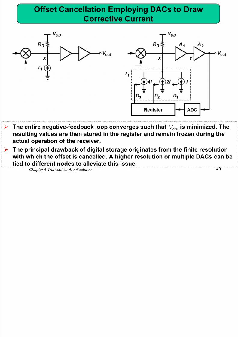
Offset Cancellation Employing DACs to Draw
8/12/2019 Chapter4 Transceiver Architectures
http://slidepdf.com/reader/full/chapter4-transceiver-architectures 49/137
Chapter 4 Transceiver Architectures 49
Offset Cancellation Employing DACs to Draw
Corrective Current
The entire negative-feedback loop converges such that V out is minimized. Theresulting values are then stored in the register and remain frozen during the
actual operation of the receiver.
The principal drawback of digital storage originates from the finite resolution
with which the offset is cancelled. A higher resolution or multiple DACs can be
tied to different nodes to alleviate this issue.
8/12/2019 Chapter4 Transceiver Architectures
http://slidepdf.com/reader/full/chapter4-transceiver-architectures 50/137
Chapter 4 Transceiver Architectures 50
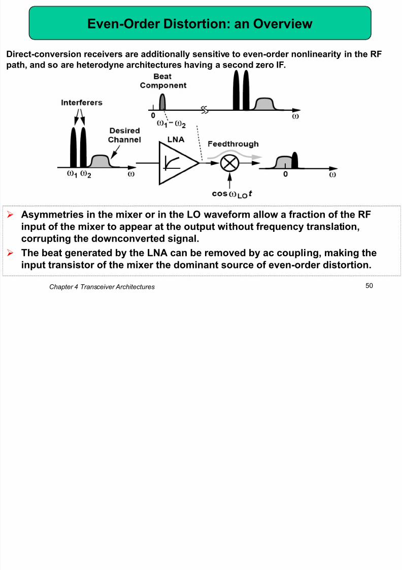
Even-Order Distortion: an Overview
Asymmetries in the mixer or in the LO waveform allow a fraction of the RFinput of the mixer to appear at the output without frequency translation,
corrupting the downconverted signal.
The beat generated by the LNA can be removed by ac coupling, making the
input transistor of the mixer the dominant source of even-order distortion.
Direct-conversion receivers are additionally sensitive to even-order nonlinearity in the RF
path, and so are heterodyne architectures having a second zero IF.
8/12/2019 Chapter4 Transceiver Architectures
http://slidepdf.com/reader/full/chapter4-transceiver-architectures 51/137
Chapter 4 Transceiver Architectures 51
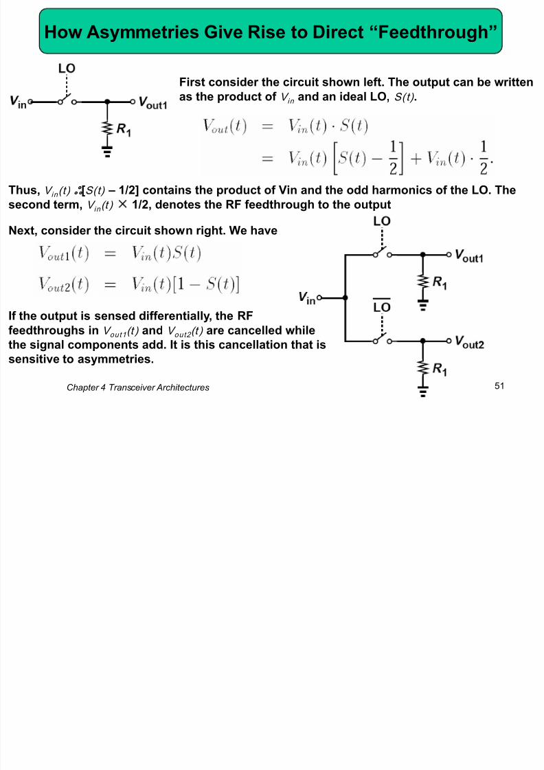
How Asymmetries Give Rise to Direct ―Feedthrough‖
First consider the circuit shown left. The output can be written
as the product of V in and an ideal LO, S(t) .
Thus, V in (t) ·[S(t) – 1/2] contains the product of Vin and the odd harmonics of the LO. Thesecond term, V in (t ) × 1/2, denotes the RF feedthrough to the output
Next, consider the circuit shown right. We have
If the output is sensed differentially, the RF
feedthroughs in V out1 (t ) and V out2 (t ) are cancelled while
the signal components add. It is this cancellation that is
sensitive to asymmetries.
S ( )
8/12/2019 Chapter4 Transceiver Architectures
http://slidepdf.com/reader/full/chapter4-transceiver-architectures 52/137
Chapter 4 Transceiver Architectures 52
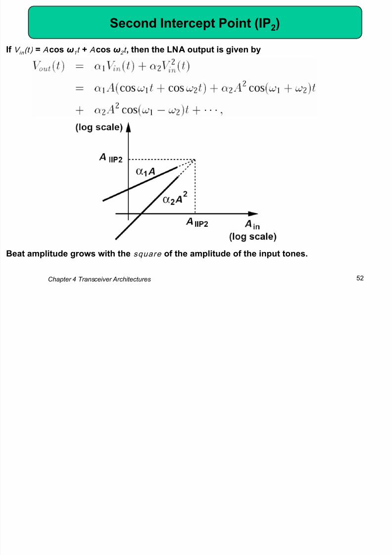
Second Intercept Point (IP2)
If V in (t ) = Acos ω1 t + Acos ω2 t , then the LNA output is given by
Beat amplitude grows with the square of the amplitude of the input tones.
E l f C l l ti f IP

8/12/2019 Chapter4 Transceiver Architectures
http://slidepdf.com/reader/full/chapter4-transceiver-architectures 53/137
Chapter 4 Transceiver Architectures 53
Example of Calculation of IP2
Solut ion:
Suppose the attenuation factor experienced by the beat as it travels through the
mixer is equal to k whereas the gain seen by each tone as it is downconverted to
the baseband is equal to unity. Calculate the IP2.
From equation above, the value of A that makes the output beat amplitude, k α 2 A2 , equal to
the main tone amplitude, α 1 A , is given by
Since the feedthrough of the beat depends on the mixer and LO asymmetries, the beat
amplitude measured in the baseband depends on the device dimensions and the layout andis therefore difficult to formulate.
hence
E O d Di t ti i th Ab f I t f

8/12/2019 Chapter4 Transceiver Architectures
http://slidepdf.com/reader/full/chapter4-transceiver-architectures 54/137
Chapter 4 Transceiver Architectures 54
Even-Order Distortion in the Absence of Interferers
Quantify the self-corruption expressed by equation above in terms of the IP2.
Assume, that the low-pass components,α 2 A 0 a(t)+ α 2 a 2 (t ) =2, experience an attenuation factor
of k and the desired signal, α 1 A 0 , sees a gain of unity. Also, typically a(t) is several times
smaller than A 0 and hence the baseband corruption can be approximated as k α 2 A 0 a(t). Thus,
the signal-to-noise ratio arising from self-corruption is given by
We express the signal as x in (t ) = [A 0 +a(t) ] cos[ωc t+ Φ (t ) ], where a(t) denotes the envelope and
typically varies slowly, i.e., it is a low-pass signal.
Both of the terms α 2 A 0 a(t) and α 2 a 2 (t)/ 2 are low-pass signals and, like the beat component,
pass through the mixer with finite attenuation, corrupting the downconverted signal.

8/12/2019 Chapter4 Transceiver Architectures
http://slidepdf.com/reader/full/chapter4-transceiver-architectures 55/137
Fli k N i

8/12/2019 Chapter4 Transceiver Architectures
http://slidepdf.com/reader/full/chapter4-transceiver-architectures 56/137
Chapter 4 Transceiver Architectures 56
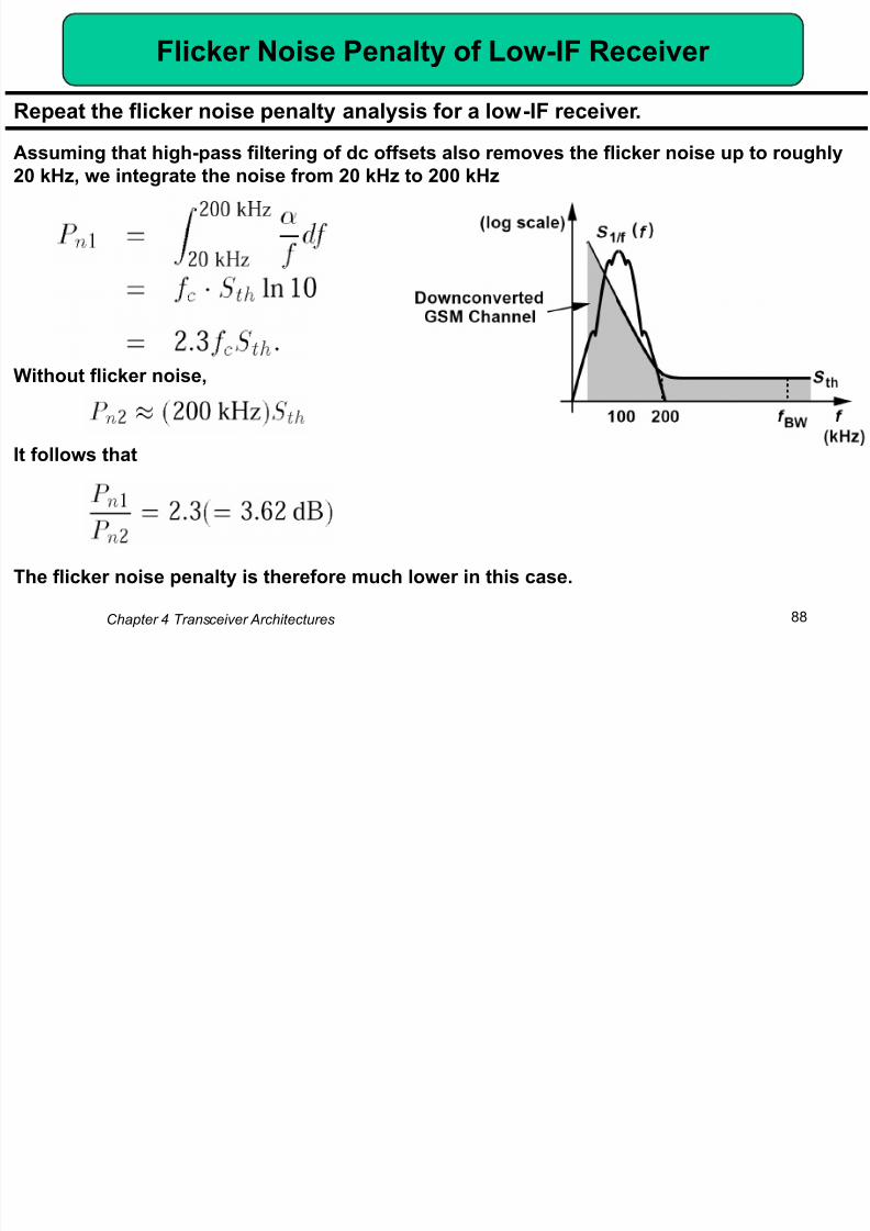
Flicker Noise
Since the signal is centered around zero frequency, it can be substantially corrupted by
flicker noise.
We note that if S 1/f = α /f , then at f c ,
An 802.11g receiver exhibits a baseband flicker noise corner frequency of 200 kHz.
Determine the flicker noise penalty
We have f BW = 10 MHz, f c = 200 kHz, and hence
E l f GSM R i Fli k N i P lt
8/12/2019 Chapter4 Transceiver Architectures
http://slidepdf.com/reader/full/chapter4-transceiver-architectures 57/137
Chapter 4 Transceiver Architectures 57
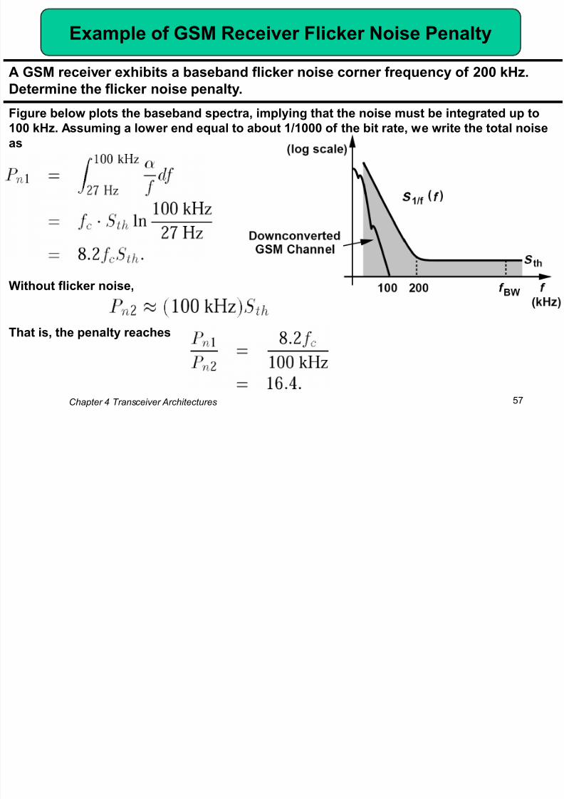
Example of GSM Receiver Flicker Noise Penalty
A GSM receiver exhibits a baseband flicker noise corner frequency of 200 kHz.
Determine the flicker noise penalty.
Figure below plots the baseband spectra, implying that the noise must be integrated up to
100 kHz. Assuming a lower end equal to about 1/1000 of the bit rate, we write the total noise
as
Without flicker noise,
That is, the penalty reaches
I/Q Mi t h S
8/12/2019 Chapter4 Transceiver Architectures
http://slidepdf.com/reader/full/chapter4-transceiver-architectures 58/137
Chapter 4 Transceiver Architectures 58
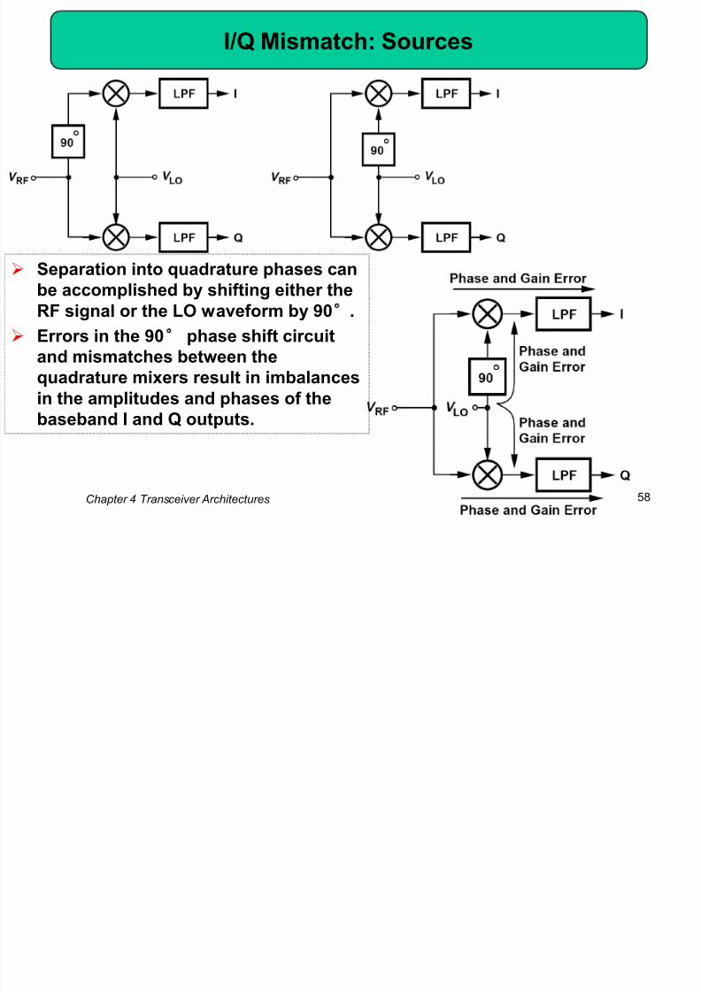
I/Q Mismatch: Sources
Separation into quadrature phases can
be accomplished by shifting either the
RF signal or the LO waveform by 90 .
Errors in the 90 phase shift circuit
and mismatches between the
quadrature mixers result in imbalancesin the amplitudes and phases of the
baseband I and Q outputs.
I/Q Mismatch in Direct-Conversion Receivers And

8/12/2019 Chapter4 Transceiver Architectures
http://slidepdf.com/reader/full/chapter4-transceiver-architectures 59/137
Chapter 4 Transceiver Architectures 59
Heterodyne Topologies
Quadrature mismatches tend to be larger in direct-conversion receivers than in
heterodyne topologies.
This occurs because
(1) the propagation of a higher frequency (f in ) through quadrature mixers
experiences greater mismatches;
(2) the quadrature phases of the LO itself suffer from greater mismatches at
higher frequencies;
Effect of I/Q Mismatch ( )
8/12/2019 Chapter4 Transceiver Architectures
http://slidepdf.com/reader/full/chapter4-transceiver-architectures 60/137
Chapter 4 Transceiver Architectures 60
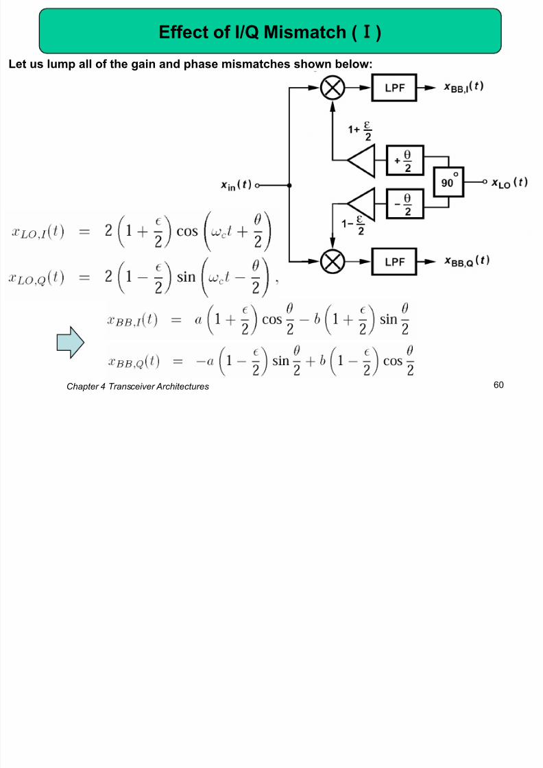
Effect of I/Q Mismatch ( )
Let us lump all of the gain and phase mismatches shown below:
Effect of I/Q Mismatch ( )
8/12/2019 Chapter4 Transceiver Architectures
http://slidepdf.com/reader/full/chapter4-transceiver-architectures 61/137
Chapter 4 Transceiver Architectures 61
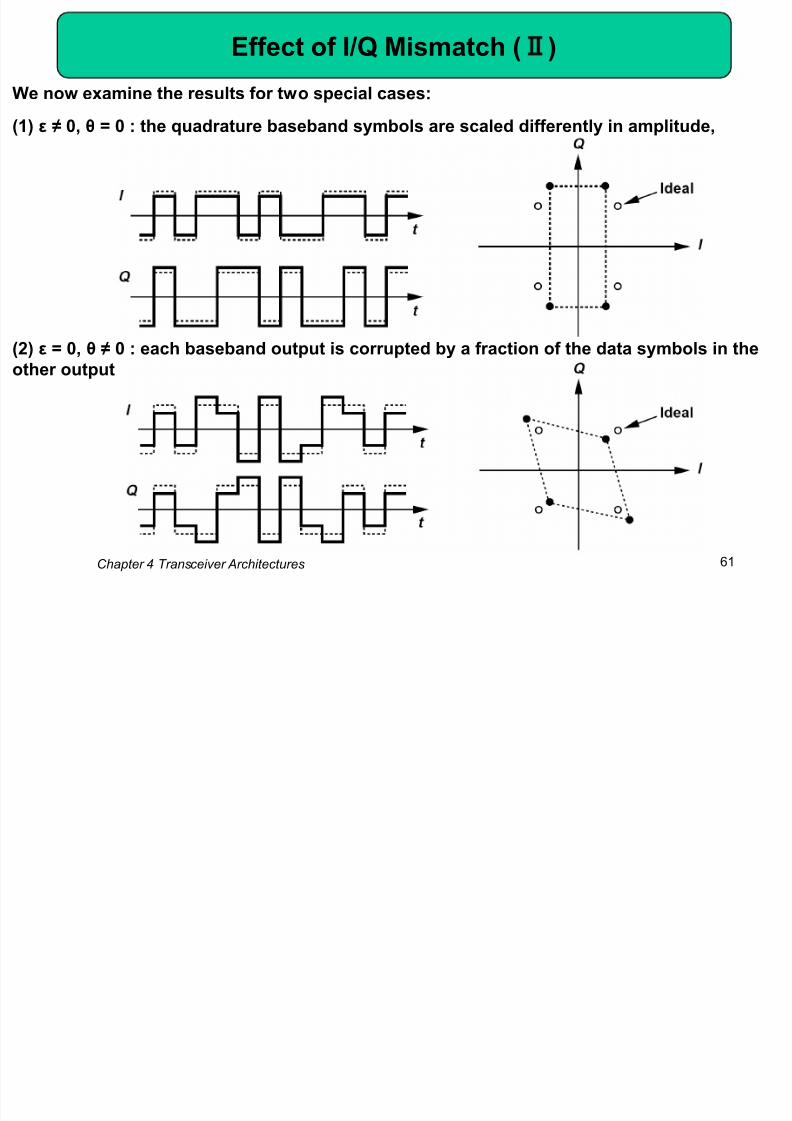
Effect of I/Q Mismatch ( )
We now examine the results for two special cases:
(1) ε ≠ 0, θ = 0 : the quadrature baseband symbols are scaled differently in amplitude,
(2) ε = 0, θ ≠ 0 : each baseband output is corrupted by a fraction of the data symbols in the
other output
Example of I/Q Mismatch ( )

8/12/2019 Chapter4 Transceiver Architectures
http://slidepdf.com/reader/full/chapter4-transceiver-architectures 62/137
Chapter 4 Transceiver Architectures 62
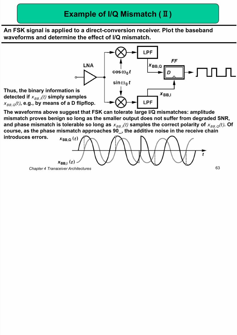
Example of I/Q Mismatch ( )
An FSK signal is applied to a direct-conversion receiver. Plot the baseband
waveforms and determine the effect of I/Q mismatch.
We express the FSK signal as x FSK (t ) = A 0 cos[(ωc + a ω1 )t ], where a = 1 represents the
binary information; i.e., the frequency of the carrier swings by +ω1 or -ω1 . Upon
multiplication by the quadrature phases of the LO, the signal produces the following
baseband components:
Figure on the right illustrates
the results: if the carrier
frequency is equal to ωc + ω1
(i.e., a = +1), then the rising
edges of x BB,I (t) coincide with
the positive peaks of x BB,Q (t).
Conversely, if the carrier
frequency is equal to ωc - ω1 ,
then the rising edges of
x BB,I (t ) coincide with the
negative peaks of x BB,Q (t ) .
Example of I/Q Mismatch ( )
8/12/2019 Chapter4 Transceiver Architectures
http://slidepdf.com/reader/full/chapter4-transceiver-architectures 63/137
Chapter 4 Transceiver Architectures 63
Example of I/Q Mismatch ( )
An FSK signal is applied to a direct-conversion receiver. Plot the baseband
waveforms and determine the effect of I/Q mismatch.
Thus, the binary information is
detected if x BB,I (t) simply samples
x BB,Q (t ) , e.g., by means of a D flipflop.
The waveforms above suggest that FSK can tolerate large I/Q mismatches: amplitude
mismatch proves benign so long as the smaller output does not suffer from degraded SNR,
and phase mismatch is tolerable so long as x BB,I (t) samples the correct polarity of x BB,Q (t ) . Ofcourse, as the phase mismatch approaches 90_, the additive noise in the receive chain
introduces errors.
Requirement of I/Q Mismatch
8/12/2019 Chapter4 Transceiver Architectures
http://slidepdf.com/reader/full/chapter4-transceiver-architectures 64/137
Chapter 4 Transceiver Architectures 64
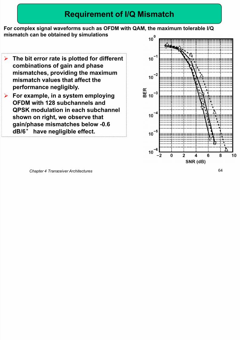
Requirement of I/Q Mismatch
For complex signal waveforms such as OFDM with QAM, the maximum tolerable I/Q
mismatch can be obtained by simulations
The bit error rate is plotted for different
combinations of gain and phase
mismatches, providing the maximum
mismatch values that affect the
performance negligibly. For example, in a system employing
OFDM with 128 subchannels and
QPSK modulation in each subchannel
shown on right, we observe that
gain/phase mismatches below -0.6
dB/6 have negligible effect.
Computation and Correction I/Q Mismatch

8/12/2019 Chapter4 Transceiver Architectures
http://slidepdf.com/reader/full/chapter4-transceiver-architectures 65/137
Chapter 4 Transceiver Architectures 65
Computation and Correction I/Q Mismatch
In many high performance systems, the quadrature phase and gain must be calibrated—
either at power-up or continuously.
Calibration at power-up can be
performed by applying an RF tone
at the input of the quadrature
mixers and observing the
baseband sinusoids in the analog
or digital domain
With the mismatches known, the
received signal constellation is
corrected before detection.
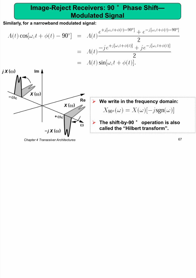
Image-Reject Receivers: 90 Phase Shift—Cosine
8/12/2019 Chapter4 Transceiver Architectures
http://slidepdf.com/reader/full/chapter4-transceiver-architectures 66/137
Chapter 4 Transceiver Architectures 66
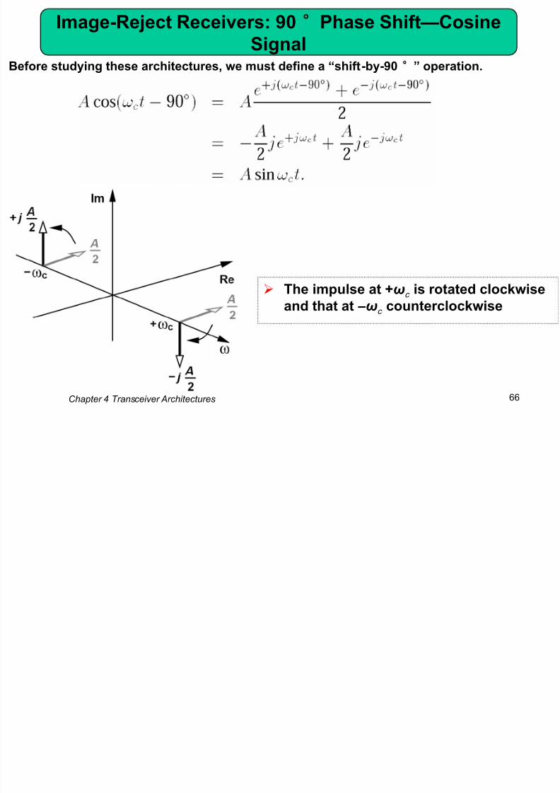
SignalBefore studying these architectures, we must define a ―shift-by-90 ‖ operation.
The impulse at +ωc is rotated clockwise
and that at –ωc counterclockwise
8/12/2019 Chapter4 Transceiver Architectures
http://slidepdf.com/reader/full/chapter4-transceiver-architectures 67/137
8/12/2019 Chapter4 Transceiver Architectures
http://slidepdf.com/reader/full/chapter4-transceiver-architectures 68/137
8/12/2019 Chapter4 Transceiver Architectures
http://slidepdf.com/reader/full/chapter4-transceiver-architectures 69/137
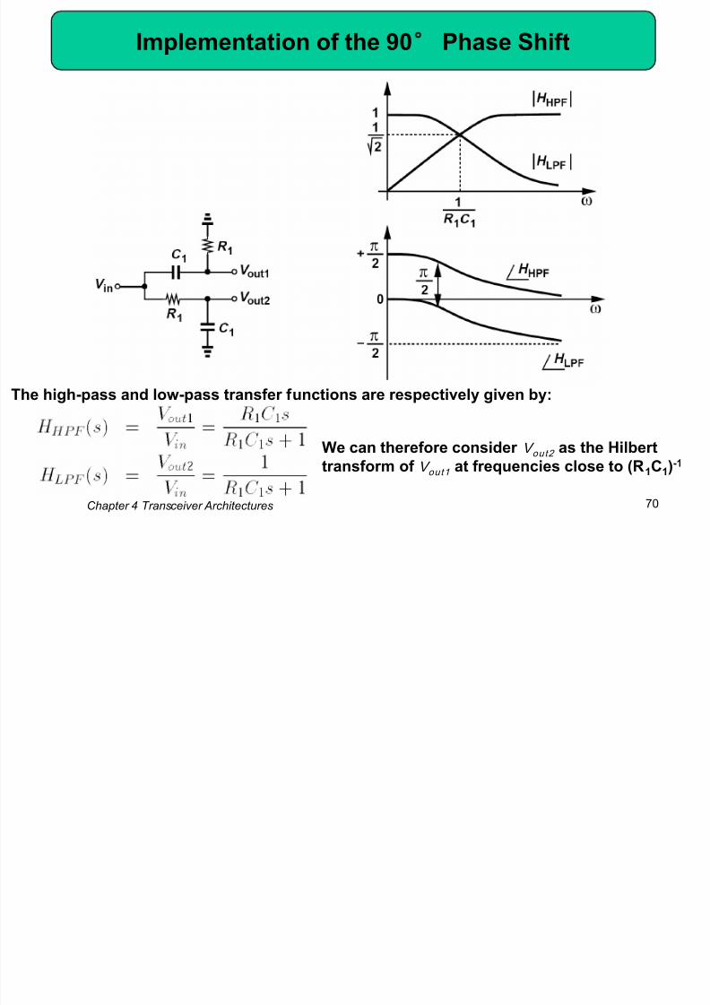
Implementation of the 90 Phase Shift
8/12/2019 Chapter4 Transceiver Architectures
http://slidepdf.com/reader/full/chapter4-transceiver-architectures 70/137
Chapter 4 Transceiver Architectures 70
Implementation of the 90 Phase Shift
The high-pass and low-pass transfer functions are respectively given by:
We can therefore consider V out2 as the Hilbert
transform of V out1 at frequencies close to (R1C1)-1
Another Approach to Implement the 90 Phase
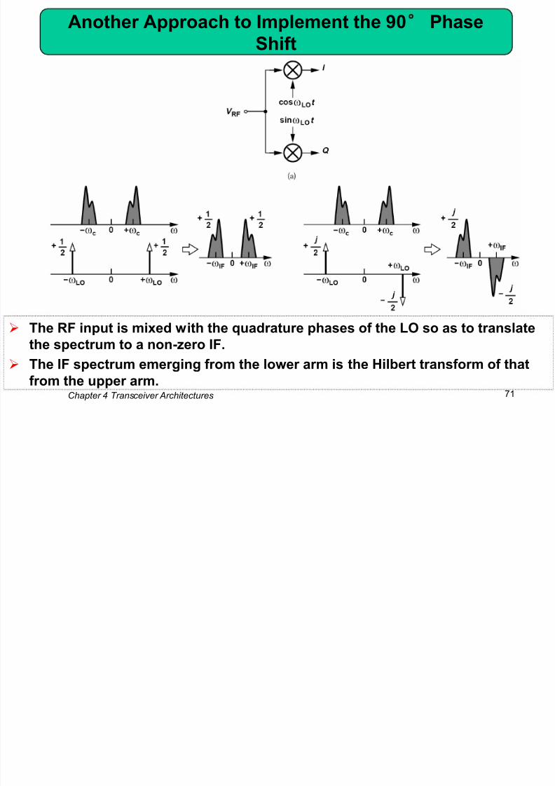
8/12/2019 Chapter4 Transceiver Architectures
http://slidepdf.com/reader/full/chapter4-transceiver-architectures 71/137
Chapter 4 Transceiver Architectures 71
Shift
The RF input is mixed with the quadrature phases of the LO so as to translate
the spectrum to a non-zero IF.
The IF spectrum emerging from the lower arm is the Hilbert transform of that
from the upper arm.
Low-Side Injection of the Above Implementation

8/12/2019 Chapter4 Transceiver Architectures
http://slidepdf.com/reader/full/chapter4-transceiver-architectures 72/137
Chapter 4 Transceiver Architectures 72
Low Side Injection of the Above Implementation
The realization above assumes high-side injection for the LO. Repeat the analysis
for low-side injection.
Figures below show the spectra for mixing with cos ωLO t and sin ωLO t , respectively. In this
case, the IF component in the lower arm is the negative of the Hilbert transform of that in the
upper arm.

8/12/2019 Chapter4 Transceiver Architectures
http://slidepdf.com/reader/full/chapter4-transceiver-architectures 73/137
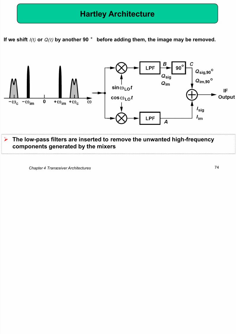
Hartley Architecture
8/12/2019 Chapter4 Transceiver Architectures
http://slidepdf.com/reader/full/chapter4-transceiver-architectures 74/137
Chapter 4 Transceiver Architectures 74
Hartley Architecture
If we shift I(t) or Q(t) by another 90 before adding them, the image may be removed.
The low-pass filters are inserted to remove the unwanted high-frequency
components generated by the mixers
8/12/2019 Chapter4 Transceiver Architectures
http://slidepdf.com/reader/full/chapter4-transceiver-architectures 75/137
Analytical Expression of Hartley’s Architecture
8/12/2019 Chapter4 Transceiver Architectures
http://slidepdf.com/reader/full/chapter4-transceiver-architectures 76/137
Chapter 4 Transceiver Architectures 76
Analytical Expression of Hartley s Architecture
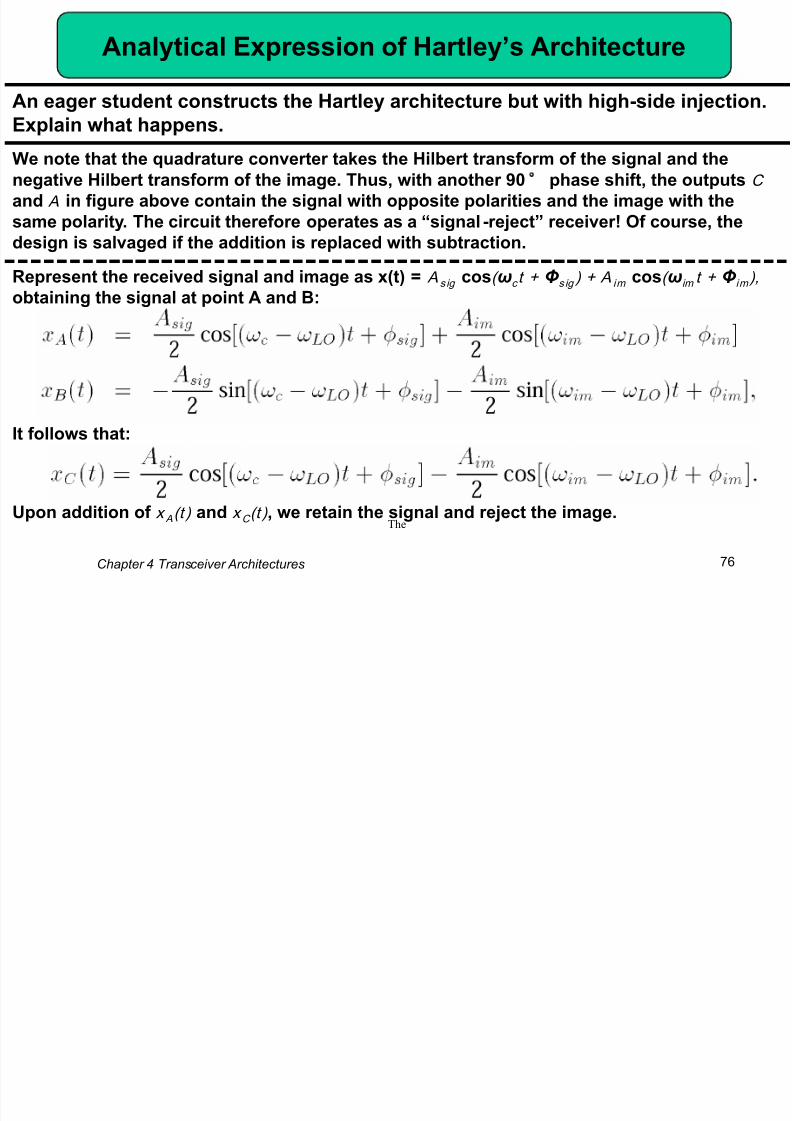
An eager student constructs the Hartley architecture but with high-side injection.
Explain what happens.
We note that the quadrature converter takes the Hilbert transform of the signal and the
negative Hilbert transform of the image. Thus, with another 90 phase shift, the outputs C
and A in figure above contain the signal with opposite polarities and the image with the
same polarity. The circuit therefore operates as a ―signal-reject‖ receiver! Of course, the
design is salvaged if the addition is replaced with subtraction.
Represent the received signal and image as x(t) = As ig
cos( ωc
t + Φ s ig
) + Aim
cos( ωim
t + Φ im
),
obtaining the signal at point A and B:
It follows that:
Upon addition of x A(t ) and x C (t ) , we retain the signal and reject the image.The
8/12/2019 Chapter4 Transceiver Architectures
http://slidepdf.com/reader/full/chapter4-transceiver-architectures 77/137
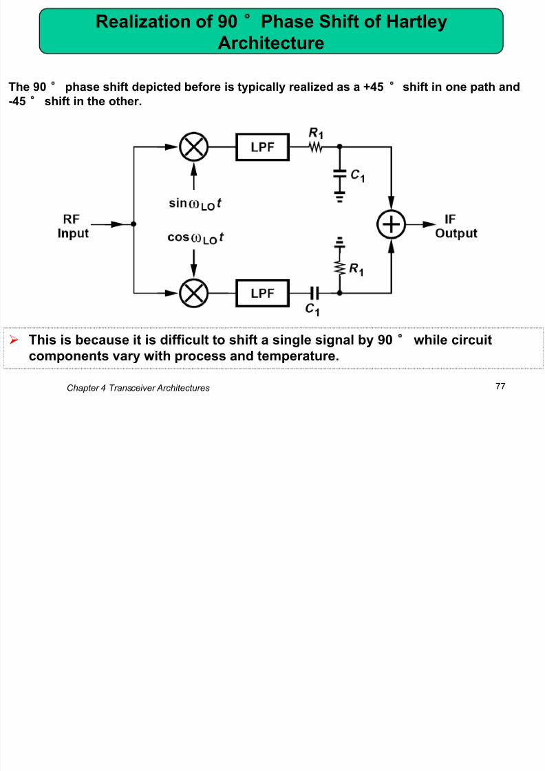
Drawbacks of Hartley Architecture ( )
8/12/2019 Chapter4 Transceiver Architectures
http://slidepdf.com/reader/full/chapter4-transceiver-architectures 78/137
Chapter 4 Transceiver Architectures 78
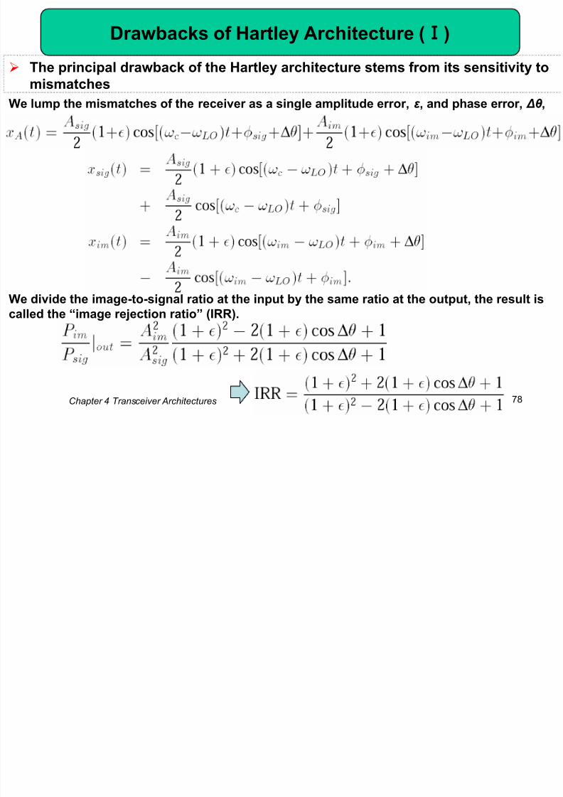
a bac s o a t ey c tectu e ( )
We lump the mismatches of the receiver as a single amplitude error, ε , and phase error, Δθ ,in the LO path, writing the downconverted signal at point A as:
We divide the image-to-signal ratio at the input by the same ratio at the output, the result iscalled the ―image rejection ratio‖ (IRR).
The principal drawback of the Hartley architecture stems from its sensitivity to
mismatches

8/12/2019 Chapter4 Transceiver Architectures
http://slidepdf.com/reader/full/chapter4-transceiver-architectures 79/137
Drawbacks of Hartley Architecture ( )
8/12/2019 Chapter4 Transceiver Architectures
http://slidepdf.com/reader/full/chapter4-transceiver-architectures 80/137
Chapter 4 Transceiver Architectures 80
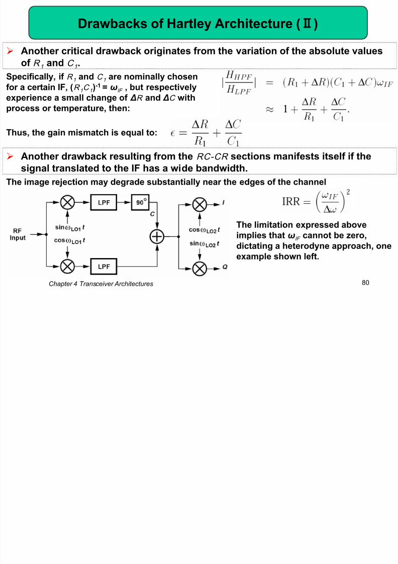
y ( )
Specifically, if R 1 and C 1 are nominally chosenfor a certain IF, (R 1 C 1 )
-1 = ωIF , but respectively
experience a small change of ΔR and ΔC with
process or temperature, then:
Thus, the gain mismatch is equal to:
Another critical drawback originates from the variation of the absolute values
of R 1 and C 1 .
Another drawback resulting from the RC-CR sections manifests itself if the
signal translated to the IF has a wide bandwidth.
The image rejection may degrade substantially near the edges of the channel
The limitation expressed above
implies that ωIF cannot be zero,
dictating a heterodyne approach, one
example shown left.
8/12/2019 Chapter4 Transceiver Architectures
http://slidepdf.com/reader/full/chapter4-transceiver-architectures 81/137
8/12/2019 Chapter4 Transceiver Architectures
http://slidepdf.com/reader/full/chapter4-transceiver-architectures 82/137
Weaver Architecture: Formulating the Circuit’s
Behavior

8/12/2019 Chapter4 Transceiver Architectures
http://slidepdf.com/reader/full/chapter4-transceiver-architectures 83/137
Chapter 4 Transceiver Architectures 83
BehaviorWe perform the second quadrature mixing operation, arriving at
Let us assume low-side injection for both mixing stages.

8/12/2019 Chapter4 Transceiver Architectures
http://slidepdf.com/reader/full/chapter4-transceiver-architectures 84/137
8/12/2019 Chapter4 Transceiver Architectures
http://slidepdf.com/reader/full/chapter4-transceiver-architectures 85/137
Double Quadrature Downconversion Weaver
Architecture

8/12/2019 Chapter4 Transceiver Architectures
http://slidepdf.com/reader/full/chapter4-transceiver-architectures 86/137
Chapter 4 Transceiver Architectures 86
Architecture
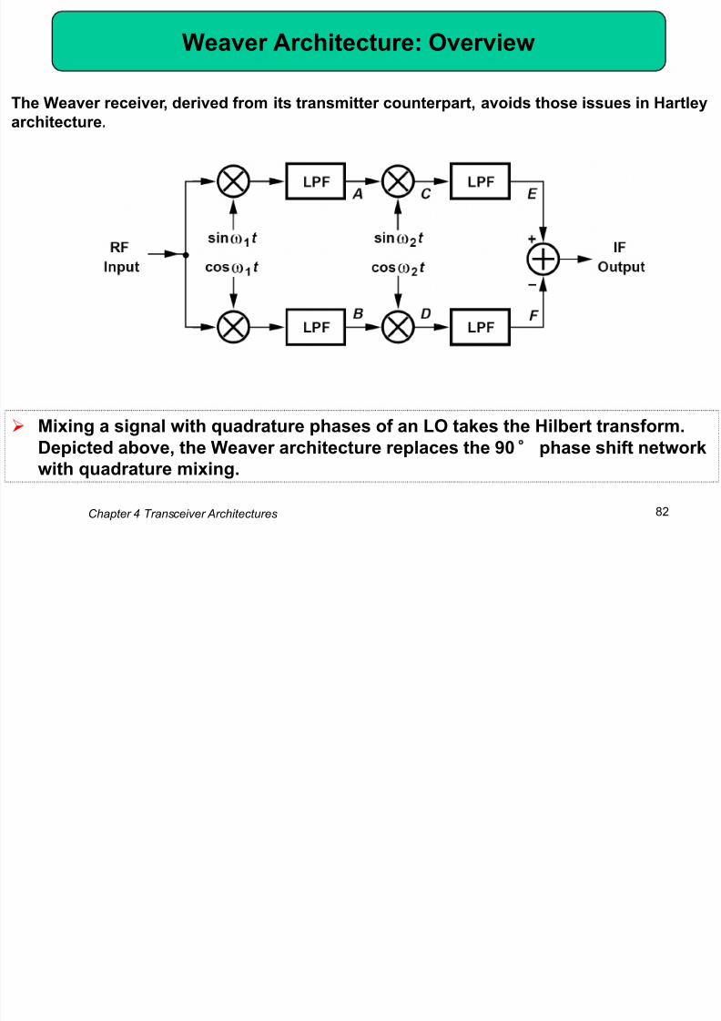
For above reason, the second downconversion preferably produces a zero IF, in which case
it must perform quadrature separation as well.
Low- IF Receivers: Overview
8/12/2019 Chapter4 Transceiver Architectures
http://slidepdf.com/reader/full/chapter4-transceiver-architectures 87/137
Chapter 4 Transceiver Architectures 87
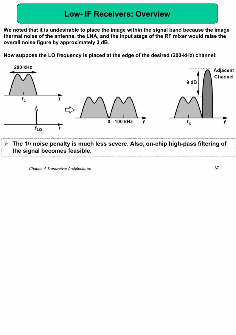
We noted that it is undesirable to place the image within the signal band because the image
thermal noise of the antenna, the LNA, and the input stage of the RF mixer would raise the
overall noise figure by approximately 3 dB.
Now suppose the LO frequency is placed at the edge of the desired (200-kHz) channel:
The 1/f noise penalty is much less severe. Also, on-chip high-pass filtering of
the signal becomes feasible.
8/12/2019 Chapter4 Transceiver Architectures
http://slidepdf.com/reader/full/chapter4-transceiver-architectures 88/137
Image Rejection in Low- IF Receivers ( )

8/12/2019 Chapter4 Transceiver Architectures
http://slidepdf.com/reader/full/chapter4-transceiver-architectures 89/137
Chapter 4 Transceiver Architectures 89
The IF spectrum in a low-IF RX may extend to zero frequency, making the Hartley
architecture impossible to maintain a high IRR across the signal bandwidth.
One possible remedy is to move the 90 phase shift in the Hartleyarchitecture from the IF path to the RF path.
The RC-CR network is centered at a high frequency and can maintain a reasonable IRR
across the band.
Image Rejection in Low- IF Receivers ( )
8/12/2019 Chapter4 Transceiver Architectures
http://slidepdf.com/reader/full/chapter4-transceiver-architectures 90/137
Chapter 4 Transceiver Architectures90
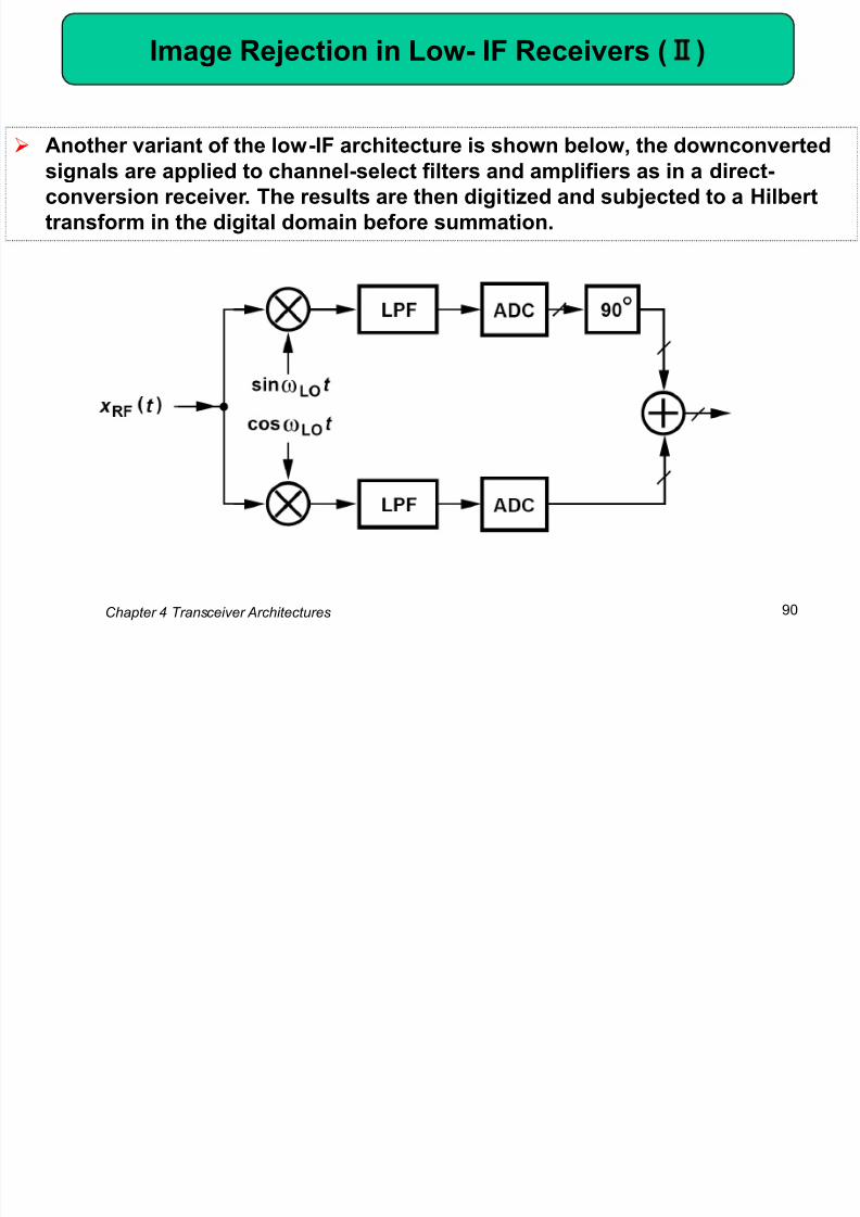
Another variant of the low-IF architecture is shown below, the downconverted
signals are applied to channel-select filters and amplifiers as in a direct-conversion receiver. The results are then digitized and subjected to a Hilbert
transform in the digital domain before summation.
8/12/2019 Chapter4 Transceiver Architectures
http://slidepdf.com/reader/full/chapter4-transceiver-architectures 91/137
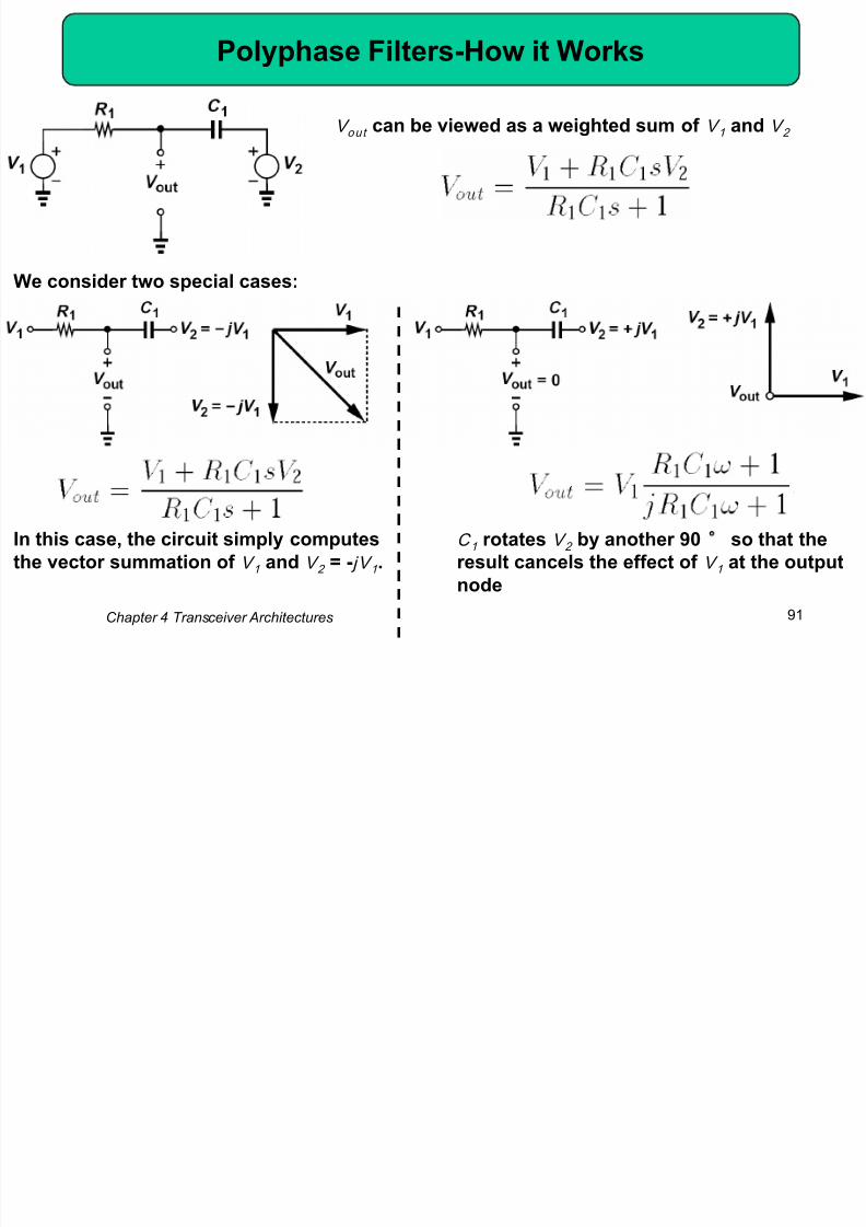
Differential Form of Polyphase Filters

8/12/2019 Chapter4 Transceiver Architectures
http://slidepdf.com/reader/full/chapter4-transceiver-architectures 92/137
Chapter 4 Transceiver Architectures92
Extend the topology above if V 1 and - jV 1 are available in differential form and
construct an image-reject receiver.
Figure below (top) shows the arrangement and the resulting phasors if R 1 = R 2 = R and C 1 =C 2 = C . The connections to quadrature downconversion mixers are depicted in figure below
(bottom).
RC Network Sensing Differential Quadrature Phases
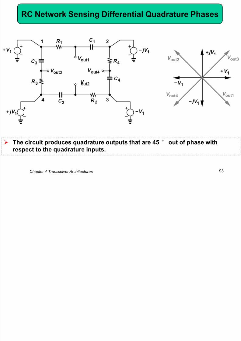
8/12/2019 Chapter4 Transceiver Architectures
http://slidepdf.com/reader/full/chapter4-transceiver-architectures 93/137
Chapter 4 Transceiver Architectures93
The circuit produces quadrature outputs that are 45 out of phase with
respect to the quadrature inputs.
Example of Quadrature Downconverter Driving RC
Sections
8/12/2019 Chapter4 Transceiver Architectures
http://slidepdf.com/reader/full/chapter4-transceiver-architectures 94/137
Chapter 4 Transceiver Architectures94
Sections
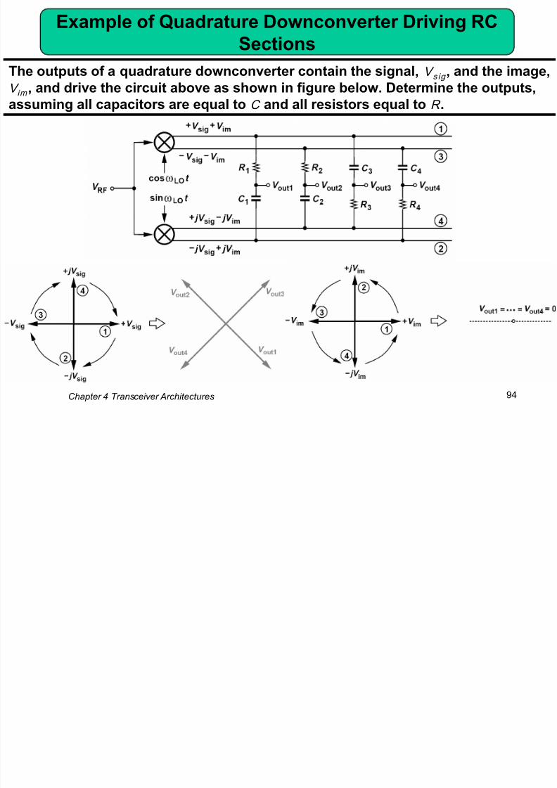
The outputs of a quadrature downconverter contain the signal, V s ig , and the image,
V im , and drive the circuit above as shown in figure below. Determine the outputs,
assuming all capacitors are equal to C and all resistors equal to R .
Effect of Polyphase Filter at a Frequency Offset
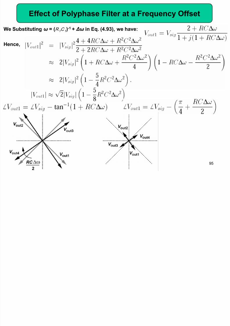
8/12/2019 Chapter4 Transceiver Architectures
http://slidepdf.com/reader/full/chapter4-transceiver-architectures 95/137
Chapter 4 Transceiver Architectures95
We Substituting ω = (R 1 C 1 )-1 + Δω in Eq. (4.93), we have:
Hence,
Cascaded Polyphase Sections- Overview
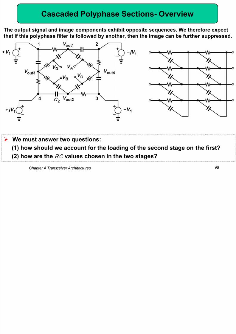
8/12/2019 Chapter4 Transceiver Architectures
http://slidepdf.com/reader/full/chapter4-transceiver-architectures 96/137
Chapter 4 Transceiver Architectures96
We must answer two questions:
(1) how should we account for the loading of the second stage on the first?
(2) how are the RC values chosen in the two stages?
The output signal and image components exhibit opposite sequences. We therefore expect
that if this polyphase filter is followed by another, then the image can be further suppressed.
Effect of Loading of Second Polyphase Section

8/12/2019 Chapter4 Transceiver Architectures
http://slidepdf.com/reader/full/chapter4-transceiver-architectures 97/137
Chapter 4 Transceiver Architectures97
If Z 1 = ··· = Z 4 = Z , then, V out1 -V out4
experience no rotation, but the loading
may reduce their magnitudes.
If RC ω = 1, the expression reduces to
Example of Loading of the Second Polyphase
Section
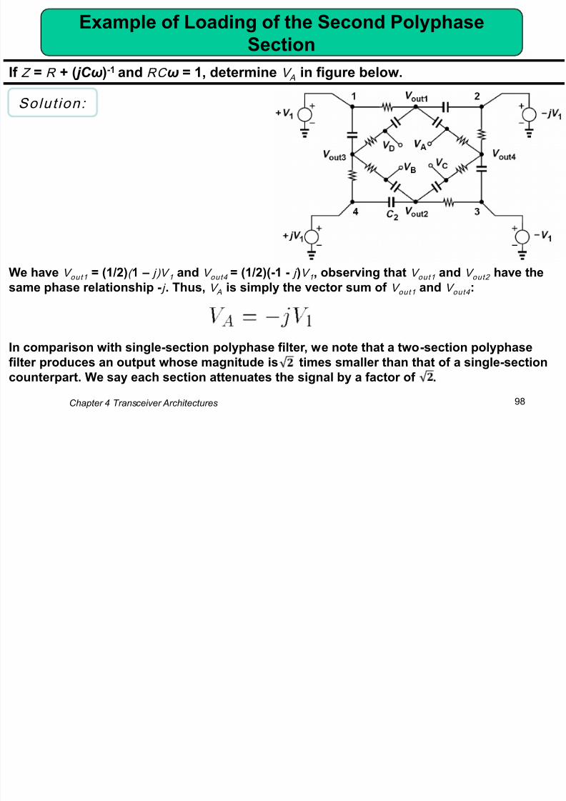
8/12/2019 Chapter4 Transceiver Architectures
http://slidepdf.com/reader/full/chapter4-transceiver-architectures 98/137
Chapter 4 Transceiver Architectures98
Section
If Z = R + ( jCω)-1 and RC ω = 1, determine V A in figure below.
We have V out1 = (1/2)( 1 – j)V 1 and V out4 = (1/2)(-1 - j )V 1 , observing that V out1 and V out2 have the
same phase relationship - j . Thus, V A is simply the vector sum of V out1 and V out4 :
In comparison with single-section polyphase filter, we note that a two-section polyphase
filter produces an output whose magnitude is times smaller than that of a single-section
counterpart. We say each section attenuates the signal by a factor of .
Solut ion:
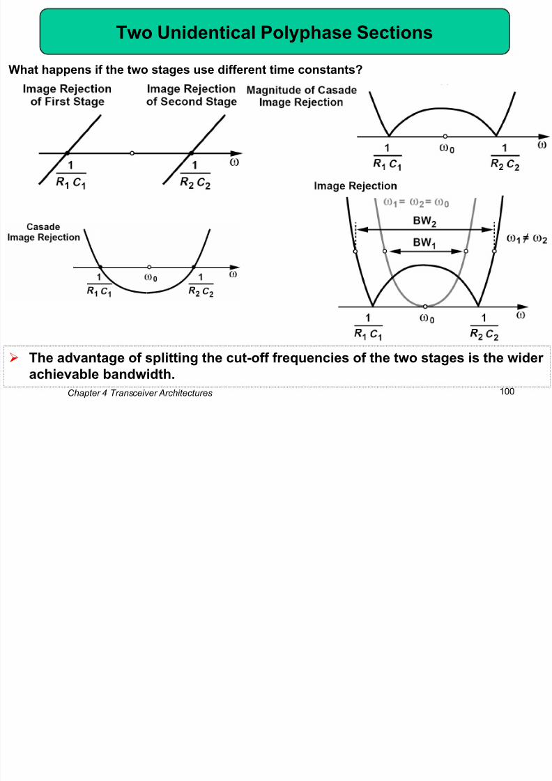
Choice of RC Values
8/12/2019 Chapter4 Transceiver Architectures
http://slidepdf.com/reader/full/chapter4-transceiver-architectures 99/137
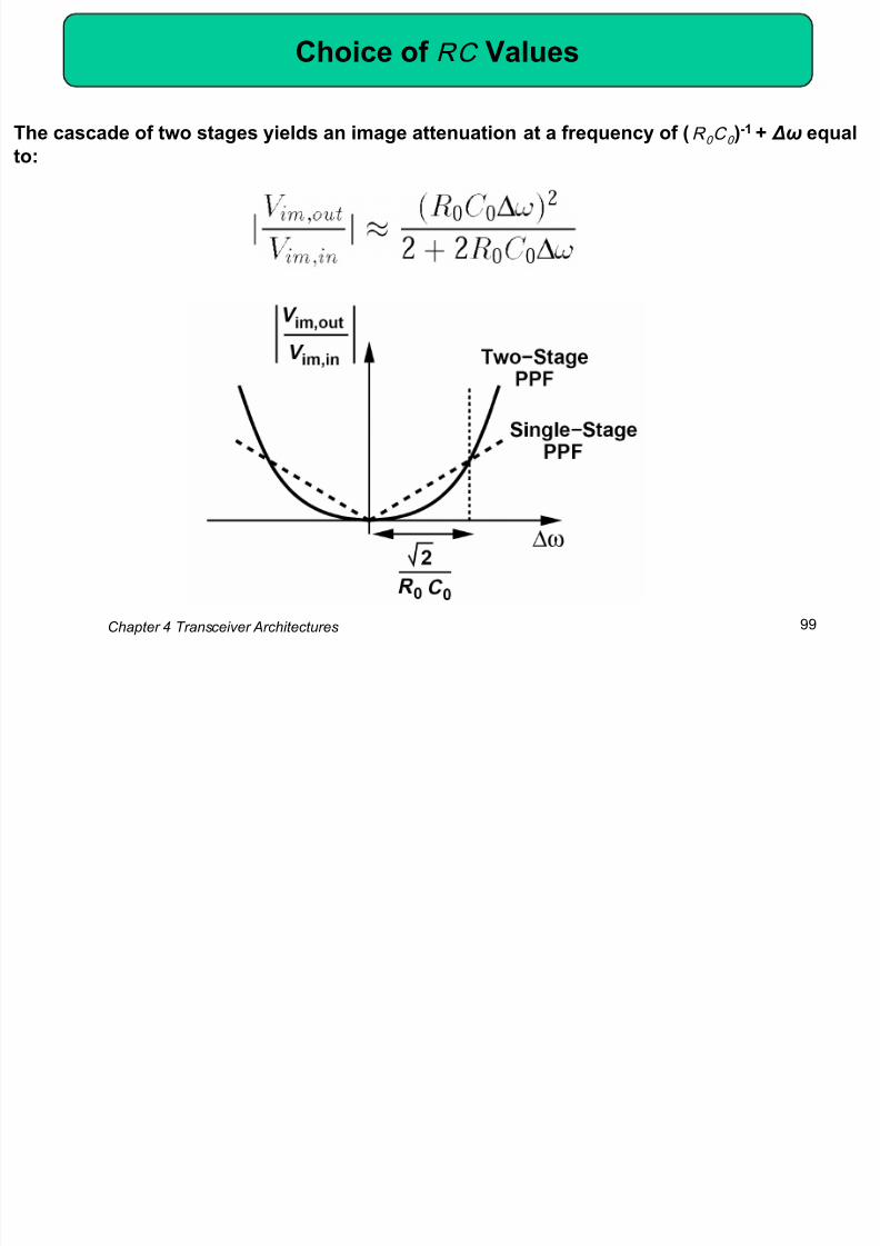
Chapter 4 Transceiver Architectures99
The cascade of two stages yields an image attenuation at a frequency of (R 0 C 0 )-1 + Δω equal
to:
8/12/2019 Chapter4 Transceiver Architectures
http://slidepdf.com/reader/full/chapter4-transceiver-architectures 100/137
Double-Quadrature Downconversion
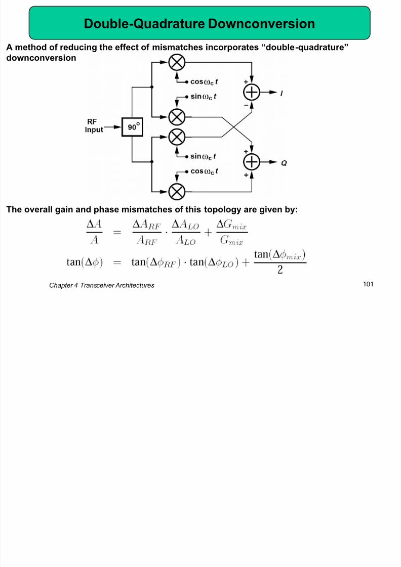
8/12/2019 Chapter4 Transceiver Architectures
http://slidepdf.com/reader/full/chapter4-transceiver-architectures 101/137
Chapter 4 Transceiver Architectures101
A method of reducing the effect of mismatches incorporates ―double-quadrature‖
downconversion
The overall gain and phase mismatches of this topology are given by:
Transmitter Architecture: General Considerations
8/12/2019 Chapter4 Transceiver Architectures
http://slidepdf.com/reader/full/chapter4-transceiver-architectures 102/137
Chapter 4 Transceiver Architectures102
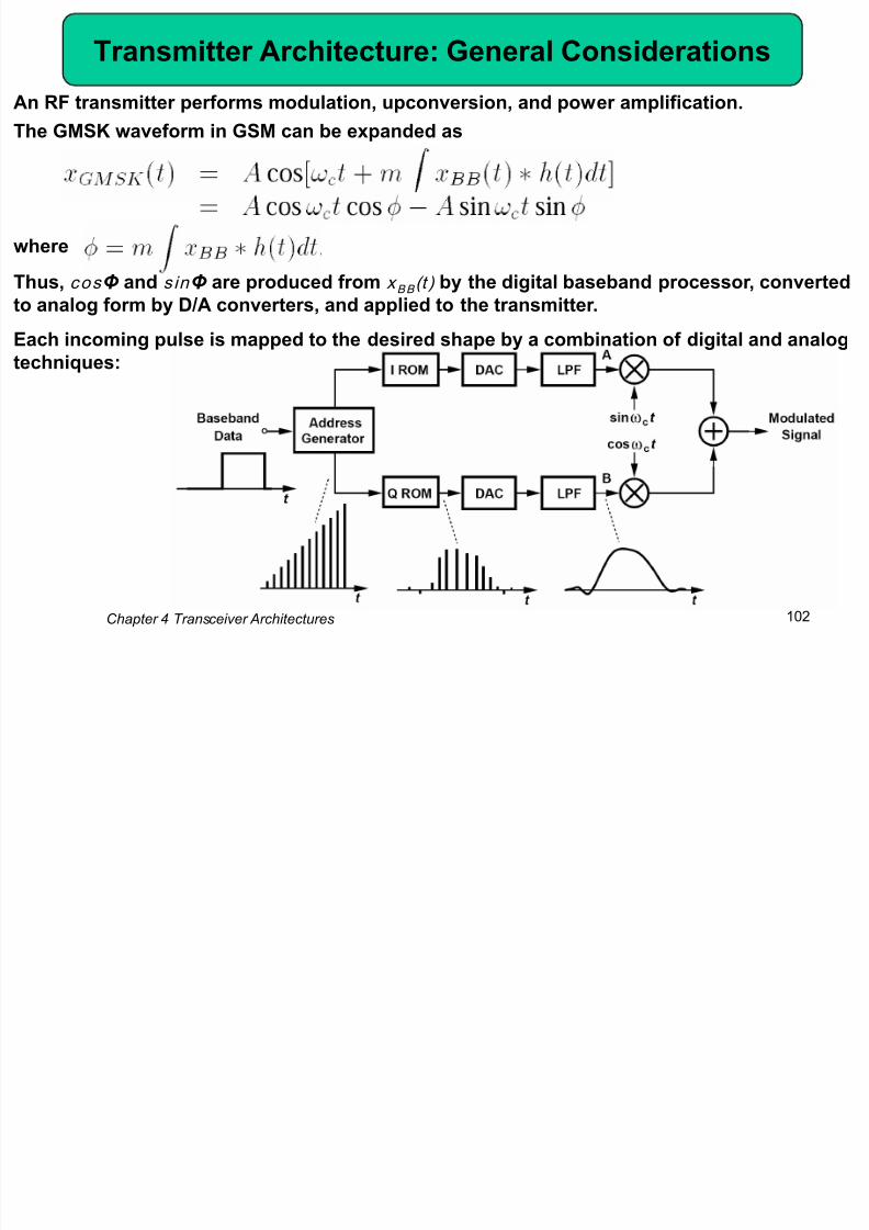
An RF transmitter performs modulation, upconversion, and power amplification.
The GMSK waveform in GSM can be expanded as
where
Thus, cos Φ and s in Φ are produced from x BB (t ) by the digital baseband processor, converted
to analog form by D/A converters, and applied to the transmitter.
Each incoming pulse is mapped to the desired shape by a combination of digital and analog
techniques:

8/12/2019 Chapter4 Transceiver Architectures
http://slidepdf.com/reader/full/chapter4-transceiver-architectures 103/137
Example of Scaling of Quadrature Upconverter
8/12/2019 Chapter4 Transceiver Architectures
http://slidepdf.com/reader/full/chapter4-transceiver-architectures 104/137
Chapter 4 Transceiver Architectures104
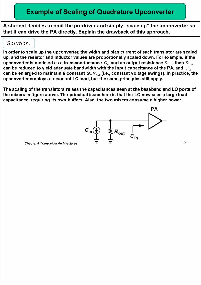
A student decides to omit the predriver and simply ―scale up‖ the upconverter so
that it can drive the PA directly. Explain the drawback of this approach.
In order to scale up the upconverter, the width and bias current of each transistor are scaled
up, and the resistor and inductor values are proportionally scaled down. For example, if the
upconverter is modeled as a transconductance G m and an output resistance R out , then R out can be reduced to yield adequate bandwidth with the input capacitance of the PA, and G m
can be enlarged to maintain a constant G m R out (i.e., constant voltage swings). In practice, theupconverter employs a resonant LC load, but the same principles still apply.
The scaling of the transistors raises the capacitances seen at the baseband and LO ports of
the mixers in figure above. The principal issue here is that the LO now sees a large load
capacitance, requiring its own buffers. Also, the two mixers consume a higher power.
Solut ion:
Direct-Conversion Transmitters: I/Q Mismatch

8/12/2019 Chapter4 Transceiver Architectures
http://slidepdf.com/reader/full/chapter4-transceiver-architectures 105/137
Chapter 4 Transceiver Architectures105
The I/Q mismatch in direct-conversion receivers results in ―cross-talk‖ between the
quadrature baseband outputs or, equivalently, distortion in the constellation.
For the four points in the constellation:
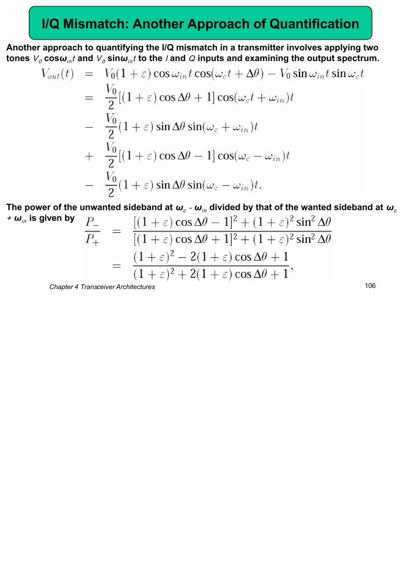
I/Q Mismatch: Another Approach of Quantification
8/12/2019 Chapter4 Transceiver Architectures
http://slidepdf.com/reader/full/chapter4-transceiver-architectures 106/137
Chapter 4 Transceiver Architectures106
Another approach to quantifying the I/Q mismatch in a transmitter involves applying two
tones V 0 cosωin t and V 0 sinωin t to the I and Q inputs and examining the output spectrum.
The power of the unwanted sideband at ωc - ωin divided by that of the wanted sideband at ωc
+ ωin is given by
I/Q Mismatch Calibration: Phase Mismatch

8/12/2019 Chapter4 Transceiver Architectures
http://slidepdf.com/reader/full/chapter4-transceiver-architectures 107/137
Chapter 4 Transceiver Architectures107
Let us now apply a single sinusoid to both inputs of the upconverter.
It can be shown that the output contains two sidebands of equal amplitudes and carries an
average power equal to:
ε is forced to zero as described above, then
I/Q Mismatch Calibration: Gain Mismatch

8/12/2019 Chapter4 Transceiver Architectures
http://slidepdf.com/reader/full/chapter4-transceiver-architectures 108/137
Chapter 4 Transceiver Architectures108
The tests entail applying a sinusoid to one baseband input while the other is set to zero.
yielding an average power of
In figure above (right):
suggesting that the gain mismatch can be adjusted so as to drive this difference to zero.
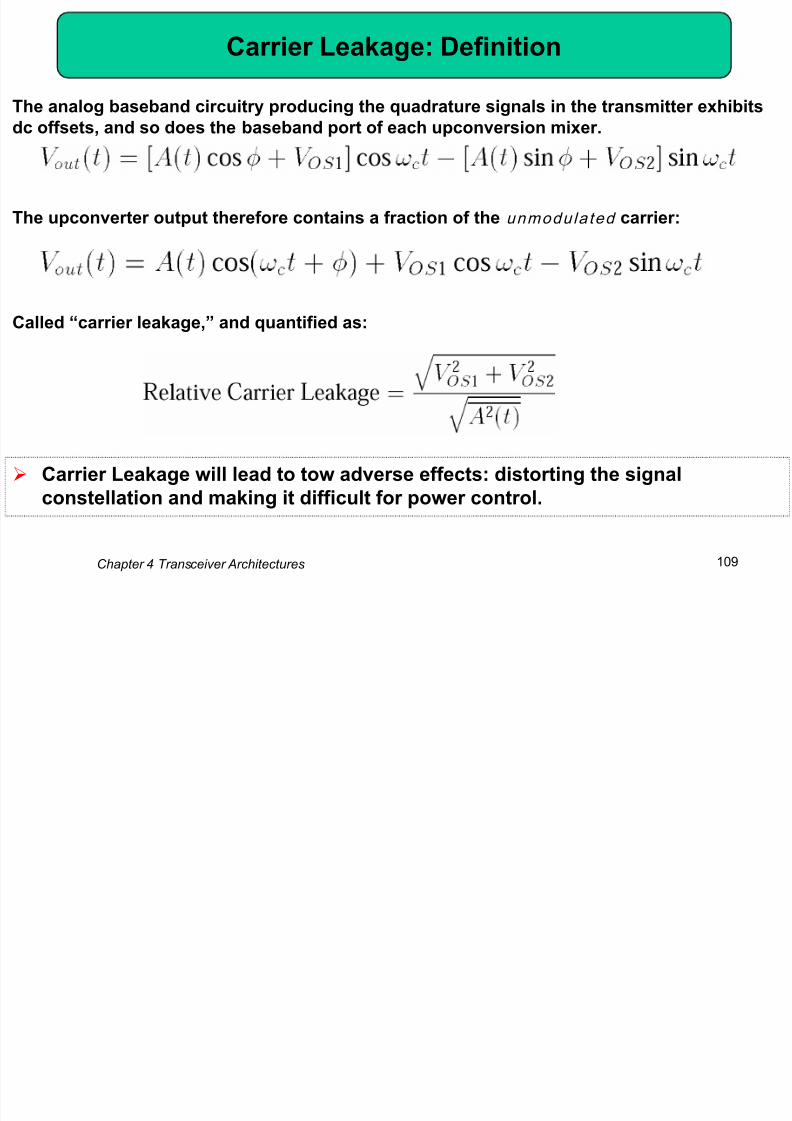
Carrier Leakage: Definition
8/12/2019 Chapter4 Transceiver Architectures
http://slidepdf.com/reader/full/chapter4-transceiver-architectures 109/137
Chapter 4 Transceiver Architectures109
The analog baseband circuitry producing the quadrature signals in the transmitter exhibits
dc offsets, and so does the baseband port of each upconversion mixer.
The upconverter output therefore contains a fraction of the unmodulated carrier:
Called ―carrier leakage,‖ and quantified as:
Carrier Leakage will lead to tow adverse effects: distorting the signal
constellation and making it difficult for power control.
Effect of Carrier Leakage( )

8/12/2019 Chapter4 Transceiver Architectures
http://slidepdf.com/reader/full/chapter4-transceiver-architectures 110/137
Chapter 4 Transceiver Architectures110
First, it distorts the signal constellation, raising the error vector magnitude at
the TX output.
For a QPSK signal:
The baseband quadrature outputs suffer from dc offsets, i.e., horizontal and vertical shifts in
the constellation.
Effect of Carrier Leakage( )
8/12/2019 Chapter4 Transceiver Architectures
http://slidepdf.com/reader/full/chapter4-transceiver-architectures 111/137
Chapter 4 Transceiver Architectures111
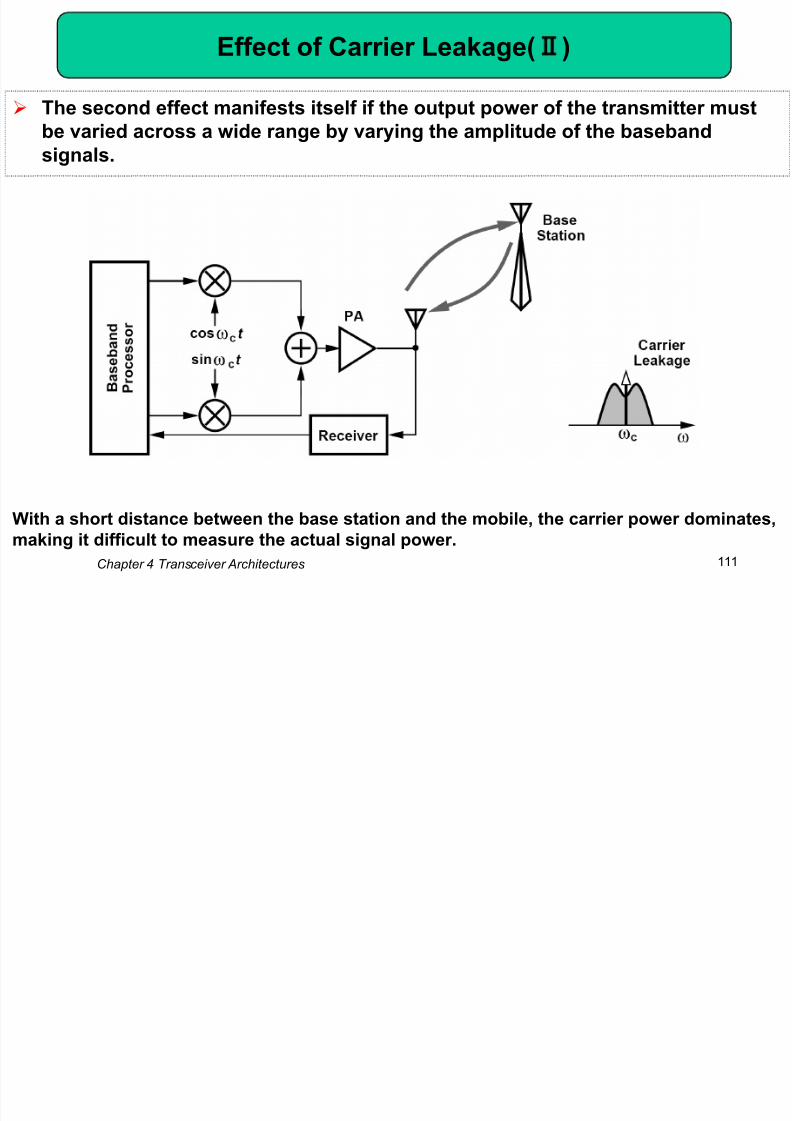
The second effect manifests itself if the output power of the transmitter must
be varied across a wide range by varying the amplitude of the baseband
signals.
With a short distance between the base station and the mobile, the carrier power dominates,
making it difficult to measure the actual signal power.
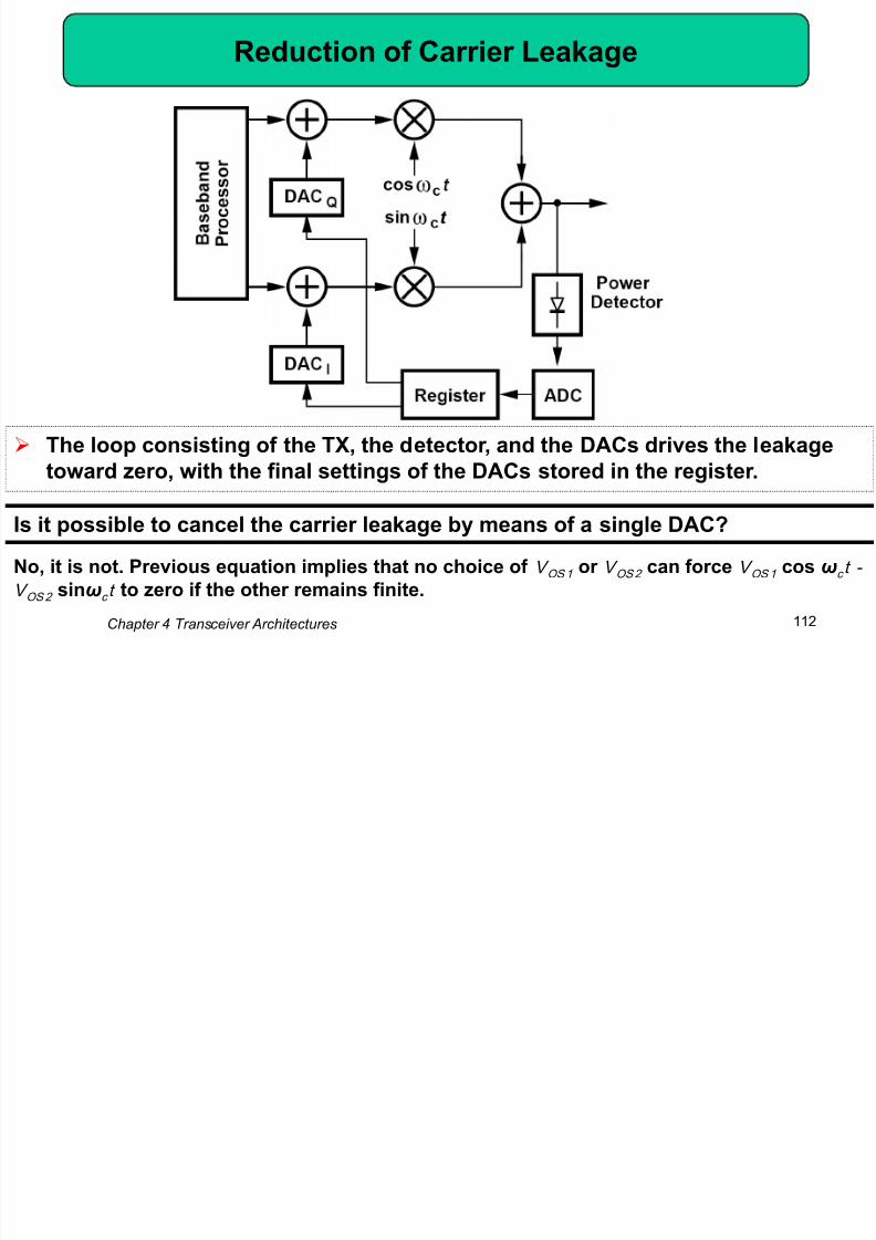
Reduction of Carrier Leakage
8/12/2019 Chapter4 Transceiver Architectures
http://slidepdf.com/reader/full/chapter4-transceiver-architectures 112/137
Chapter 4 Transceiver Architectures112
The loop consisting of the TX, the detector, and the DACs drives the leakage
toward zero, with the final settings of the DACs stored in the register.
Is it possible to cancel the carrier leakage by means of a single DAC?
No, it is not. Previous equation implies that no choice of V OS1 or V OS2 can force V OS1 cos ωc t -
V OS2 sinωc t to zero if the other remains finite.
Mixer Linearity
8/12/2019 Chapter4 Transceiver Architectures
http://slidepdf.com/reader/full/chapter4-transceiver-architectures 113/137
Chapter 4 Transceiver Architectures113
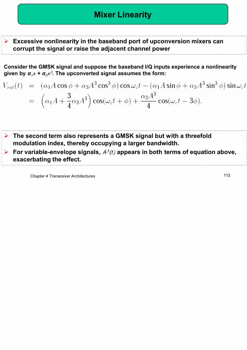
Consider the GMSK signal and suppose the baseband I/Q inputs experience a nonlinearity
given by α 1 x + α 3 x 3 . The upconverted signal assumes the form:
Excessive nonlinearity in the baseband port of upconversion mixers can
corrupt the signal or raise the adjacent channel power
The second term also represents a GMSK signal but with a threefoldmodulation index, thereby occupying a larger bandwidth.
For variable-envelope signals, A 3 (t ) appears in both terms of equation above,
exacerbating the effect.
TX Linearity
8/12/2019 Chapter4 Transceiver Architectures
http://slidepdf.com/reader/full/chapter4-transceiver-architectures 114/137
Chapter 4 Transceiver Architectures114
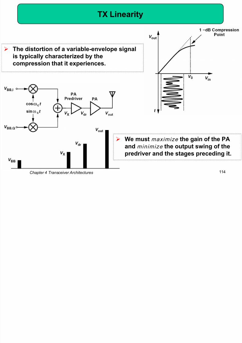
The distortion of a variable-envelope signalis typically characterized by the
compression that it experiences.
We must maximize the gain of the PA
and minimize the output swing of the
predriver and the stages preceding it.
Example of TX Linearity
8/12/2019 Chapter4 Transceiver Architectures
http://slidepdf.com/reader/full/chapter4-transceiver-architectures 115/137
Chapter 4 Transceiver Architectures115
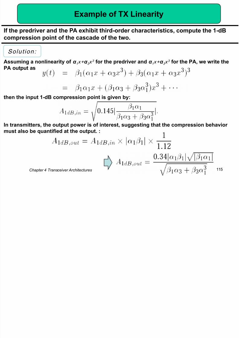
If the predriver and the PA exhibit third-order characteristics, compute the 1-dB
compression point of the cascade of the two.
Assuming a nonlinearity of α 1 x+ α 3 x 3 for the predriver and α 1 x+ α 3 x
3 for the PA, we write the
PA output as
Solut ion:
then the input 1-dB compression point is given by:
In transmitters, the output power is of interest, suggesting that the compression behavior
must also be quantified at the output. :
Oscillator Pulling

8/12/2019 Chapter4 Transceiver Architectures
http://slidepdf.com/reader/full/chapter4-transceiver-architectures 116/137
Chapter 4 Transceiver Architectures116
The PA output exhibits very large swings, which couple to various parts of the
system through the silicon substrate, package parasitics, and traces on theprinted-circuit board. Thus, it is likely that an appreciable fraction of the PA
output couples to the local oscillator.
Effect of Oscillator Pulling
8/12/2019 Chapter4 Transceiver Architectures
http://slidepdf.com/reader/full/chapter4-transceiver-architectures 117/137
Chapter 4 Transceiver Architectures 117
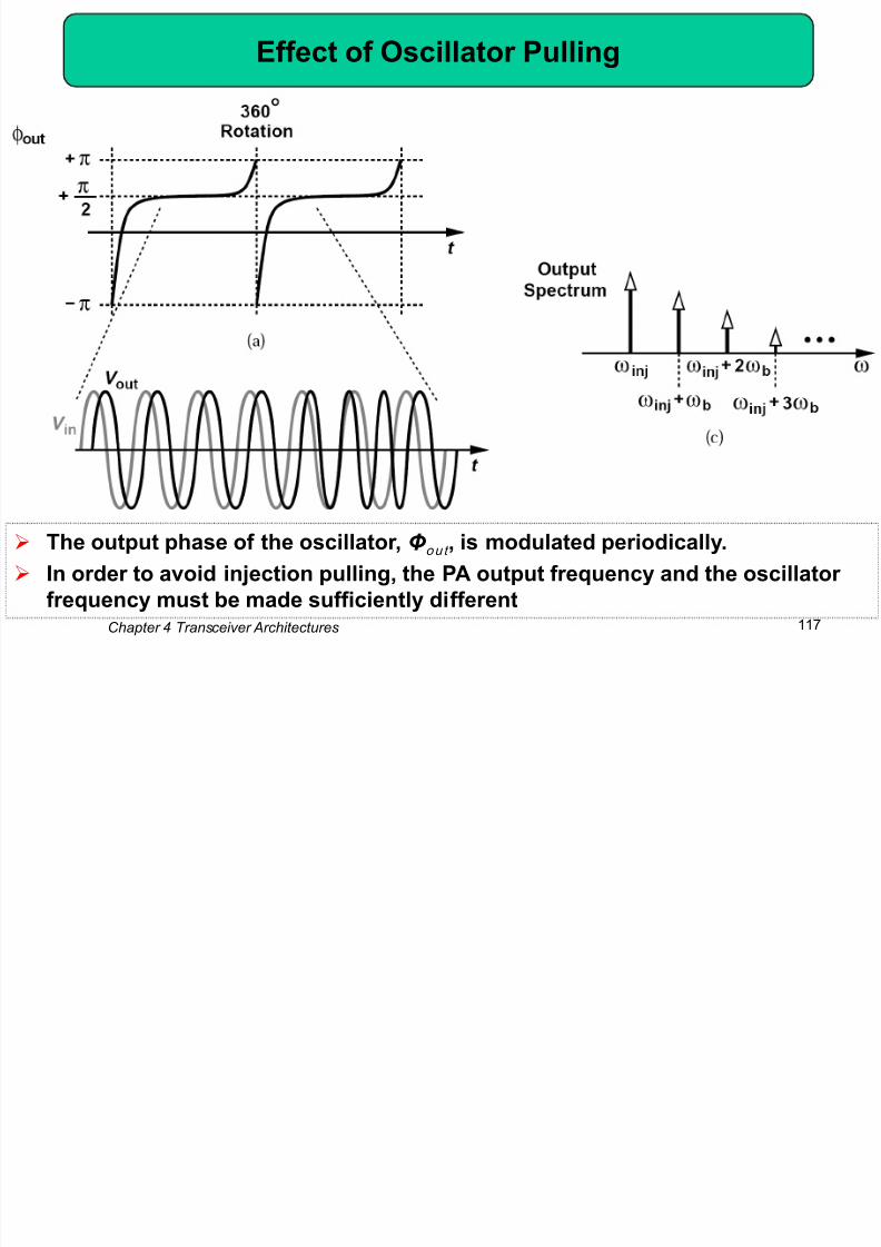
The output phase of the oscillator, Φ out , is modulated periodically.
In order to avoid injection pulling, the PA output frequency and the oscillator
frequency must be made sufficiently different
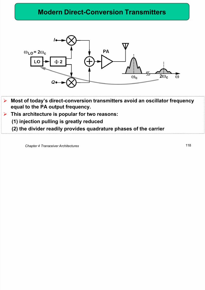
Modern Direct-Conversion Transmitters
8/12/2019 Chapter4 Transceiver Architectures
http://slidepdf.com/reader/full/chapter4-transceiver-architectures 118/137
Chapter 4 Transceiver Architectures 118
Most of today’s direct-conversion transmitters avoid an oscillator frequency
equal to the PA output frequency.
This architecture is popular for two reasons:
(1) injection pulling is greatly reduced
(2) the divider readily provides quadrature phases of the carrier
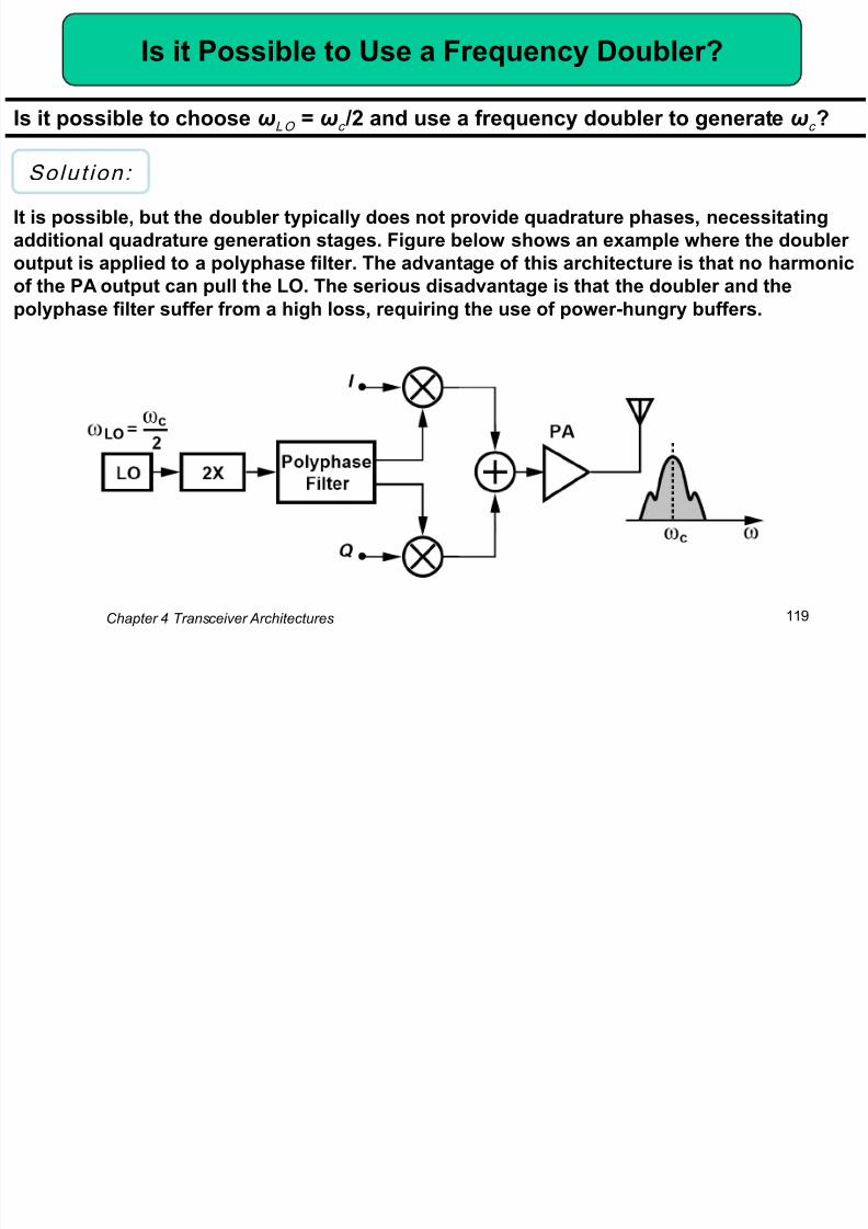
Is it Possible to Use a Frequency Doubler?
8/12/2019 Chapter4 Transceiver Architectures
http://slidepdf.com/reader/full/chapter4-transceiver-architectures 119/137
Chapter 4 Transceiver Architectures 119
Is it possible to choose ωLO = ωc /2 and use a frequency doubler to generate ωc ?
It is possible, but the doubler typically does not provide quadrature phases, necessitating
additional quadrature generation stages. Figure below shows an example where the doubler
output is applied to a polyphase filter. The advantage of this architecture is that no harmonic
of the PA output can pull the LO. The serious disadvantage is that the doubler and the
polyphase filter suffer from a high loss, requiring the use of power-hungry buffers.
Solut ion:
Use Mixing to Derive Frequencies

8/12/2019 Chapter4 Transceiver Architectures
http://slidepdf.com/reader/full/chapter4-transceiver-architectures 120/137
Chapter 4 Transceiver Architectures 120
The oscillator frequency is divided by 2 and the two outputs are mixed. The
result contains components at ω1 ω1/2 with equal magnitudes.
Can both components be retained?
(1) half of the power delivered to the antenna is wasted.
(2) the power transmitted at the unwanted carrier frequency corrupts
communication in other channels or bands.
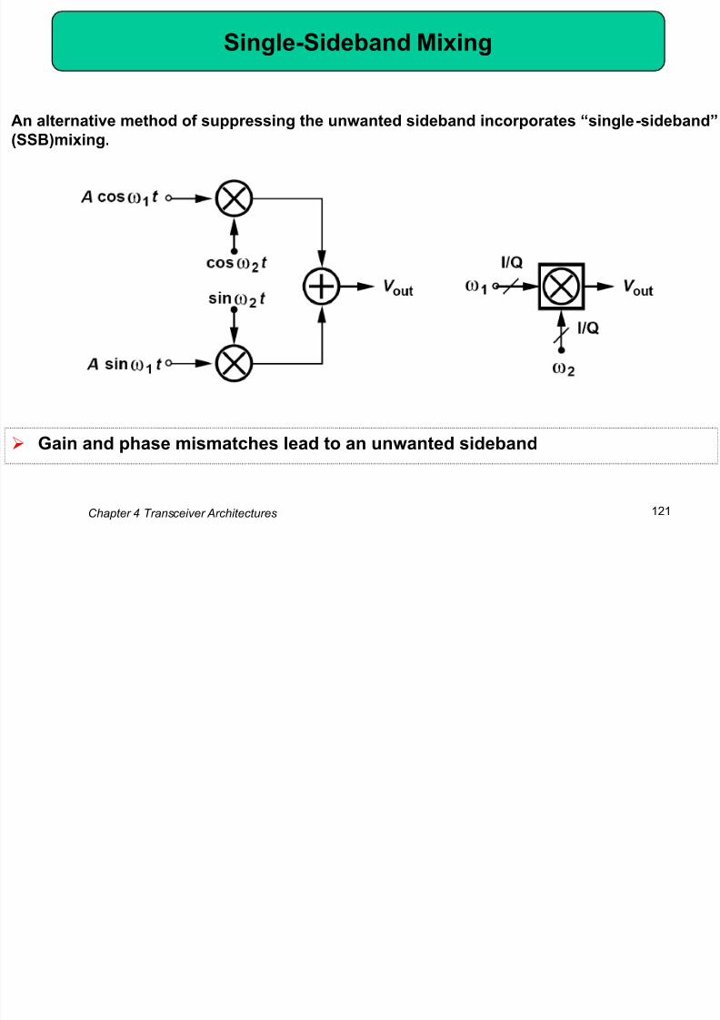
Single-Sideband Mixing
8/12/2019 Chapter4 Transceiver Architectures
http://slidepdf.com/reader/full/chapter4-transceiver-architectures 121/137
Chapter 4 Transceiver Architectures 121
An alternative method of suppressing the unwanted sideband incorporates ―single-sideband‖
(SSB)mixing.
Gain and phase mismatches lead to an unwanted sideband
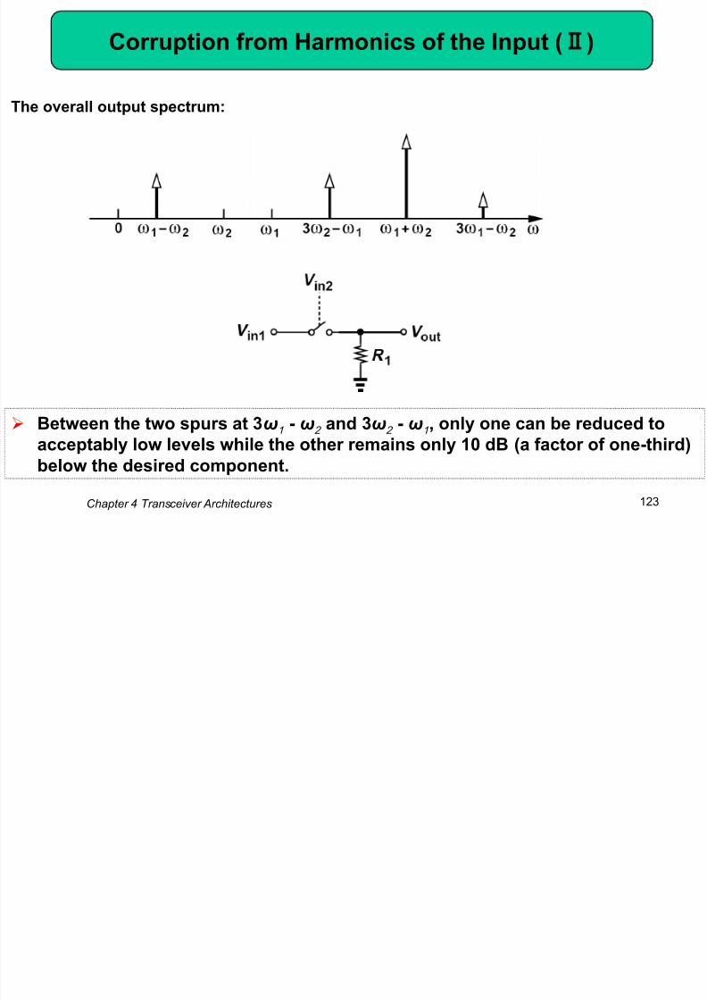
Corruption from Harmonics of the Input ( )

8/12/2019 Chapter4 Transceiver Architectures
http://slidepdf.com/reader/full/chapter4-transceiver-architectures 122/137
Chapter 4 Transceiver Architectures 122
Suppose each mixer exhibits third-order nonlinearity If the nonlinearity is of the form
α 1 x+ α 3 x 3 ,
The output spectrum contains a spur at 3ω1 - ω2 . Similarly, with third-order
nonlinearity in the mixer ports sensing sin ω2 t and cos ω2 t , a component at
3ω2 - ω1 arises at the output.
8/12/2019 Chapter4 Transceiver Architectures
http://slidepdf.com/reader/full/chapter4-transceiver-architectures 123/137
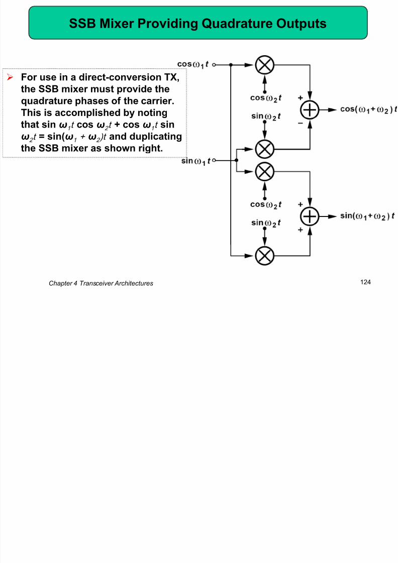
SSB Mixer Providing Quadrature Outputs
8/12/2019 Chapter4 Transceiver Architectures
http://slidepdf.com/reader/full/chapter4-transceiver-architectures 124/137
Chapter 4 Transceiver Architectures 124
For use in a direct-conversion TX,the SSB mixer must provide the
quadrature phases of the carrier.
This is accomplished by noting
that sin ω1 t cos ω2 t + cos ω1 t sin
ω2 t = sin(ω1 + ω2 )t and duplicating
the SSB mixer as shown right.
Direct-Conversion TX Using SSB Mixing in LO Path

8/12/2019 Chapter4 Transceiver Architectures
http://slidepdf.com/reader/full/chapter4-transceiver-architectures 125/137
Chapter 4 Transceiver Architectures 125
Since the carrier and LO frequencies are sufficiently different, this architecture
remains free from injection pulling.
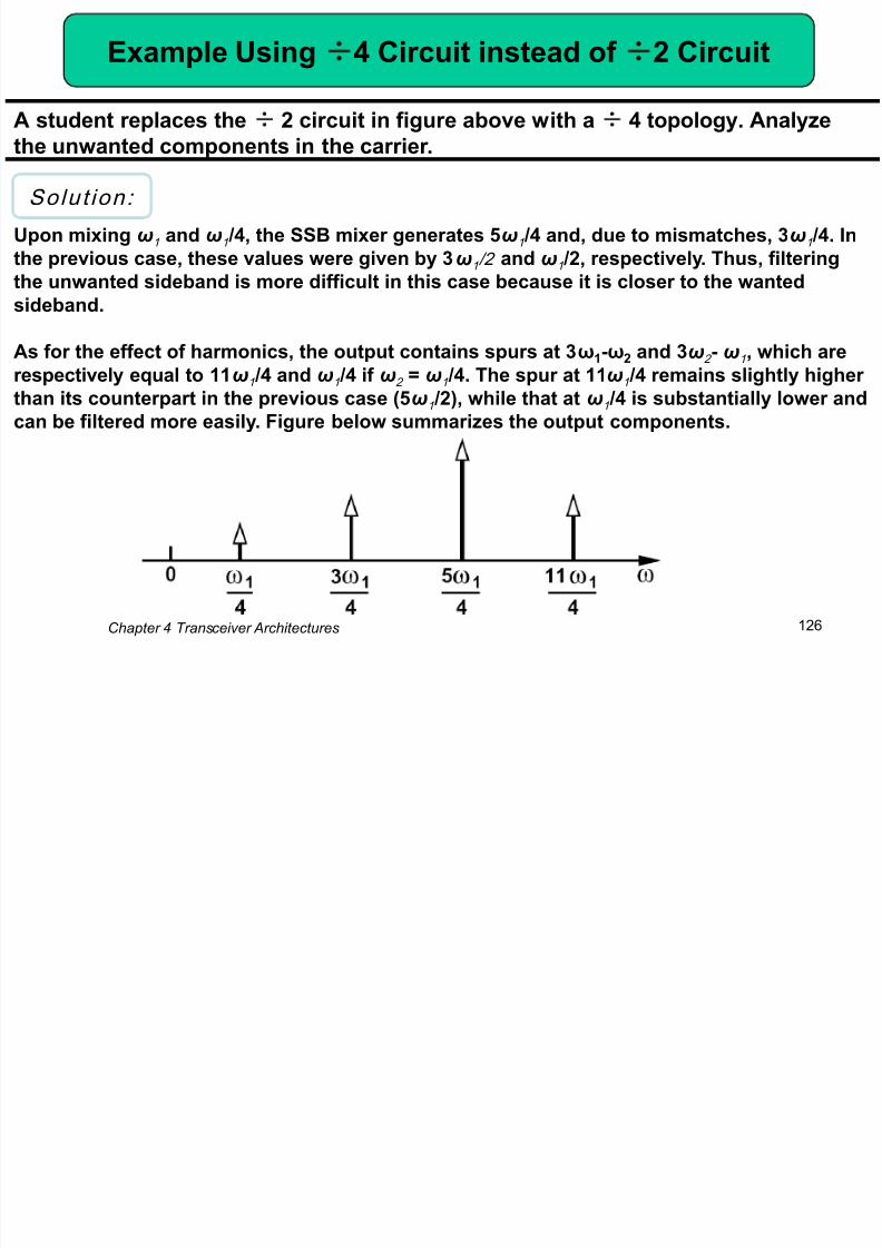
Example Using÷4 Circuit instead of÷2 Circuit
8/12/2019 Chapter4 Transceiver Architectures
http://slidepdf.com/reader/full/chapter4-transceiver-architectures 126/137
Chapter 4 Transceiver Architectures 126
A student replaces the÷ 2 circuit in figure above with a÷ 4 topology. Analyze
the unwanted components in the carrier.
Upon mixing ω1 and ω1 /4, the SSB mixer generates 5ω1 /4 and, due to mismatches, 3ω1 /4. In
the previous case, these values were given by 3ω1 /2 and ω1 /2, respectively. Thus, filtering
the unwanted sideband is more difficult in this case because it is closer to the wanted
sideband.
As for the effect of harmonics, the output contains spurs at 3ω1-ω2 and 3ω2 - ω1 , which are
respectively equal to 11ω1 /4 and ω1 /4 if ω2 = ω1 /4. The spur at 11ω1 /4 remains slightly higher
than its counterpart in the previous case (5ω1 /2), while that at ω1 /4 is substantially lower and
can be filtered more easily. Figure below summarizes the output components.
Solut ion:
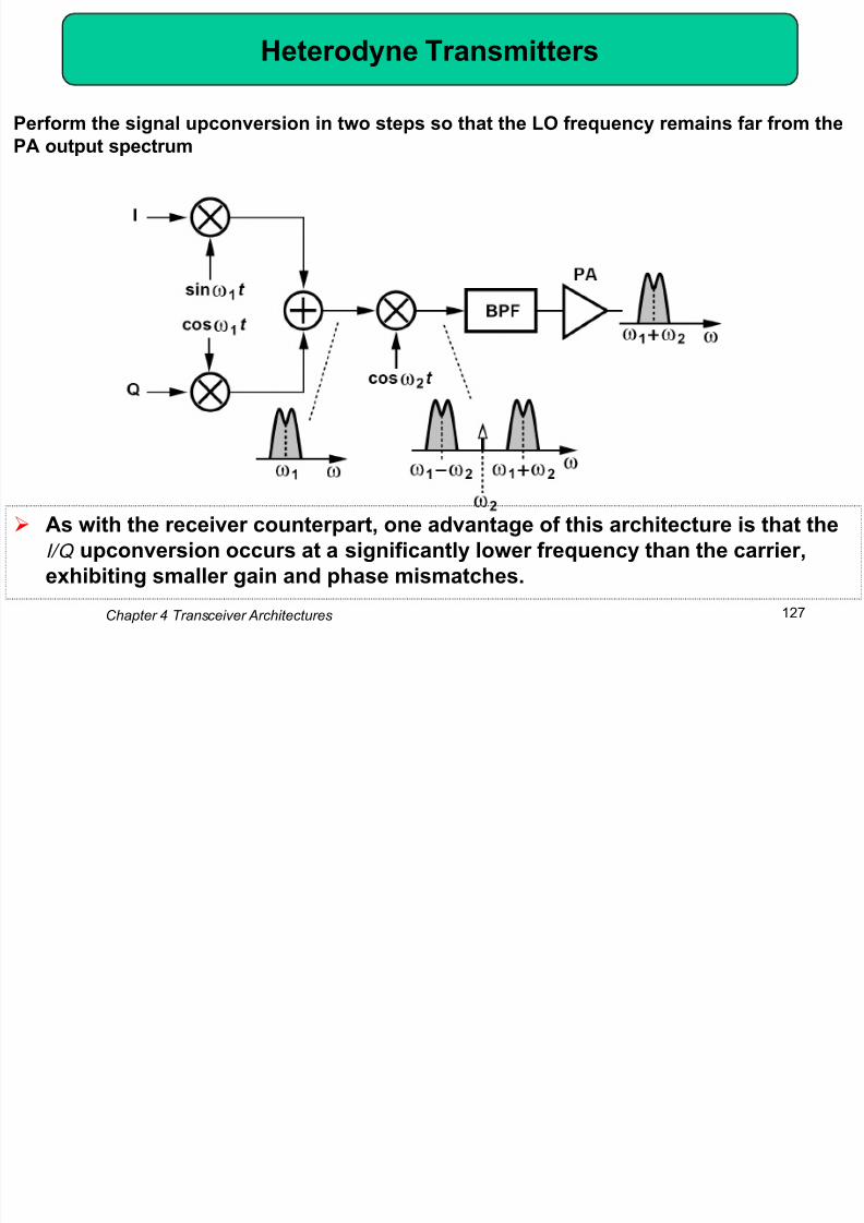
Heterodyne Transmitters
8/12/2019 Chapter4 Transceiver Architectures
http://slidepdf.com/reader/full/chapter4-transceiver-architectures 127/137
Chapter 4 Transceiver Architectures 127
Perform the signal upconversion in two steps so that the LO frequency remains far from the
PA output spectrum
As with the receiver counterpart, one advantage of this architecture is that the
I/Q upconversion occurs at a significantly lower frequency than the carrier,
exhibiting smaller gain and phase mismatches.
Sliding-IF TX

8/12/2019 Chapter4 Transceiver Architectures
http://slidepdf.com/reader/full/chapter4-transceiver-architectures 128/137
Chapter 4 Transceiver Architectures 128
In analogy with the sliding-IF receiver architecture, we eliminate the first oscillator in the
above TX and derive the required phases from the second oscillator
We call the LO waveforms at ω1 /2 and ω1 the first and second LOs, respectively.
Carrier Leakage

8/12/2019 Chapter4 Transceiver Architectures
http://slidepdf.com/reader/full/chapter4-transceiver-architectures 129/137
Chapter 4 Transceiver Architectures 129
The dc offsets in the baseband yield a component at ω1
/2 at the output of the
quadrature upconverter, and the dc offset at the input of the RF mixer
produces another component at ω1
The former can be minimized as described before. The latter, and the lower
sideband at ω1 /2, must be removed by filtering
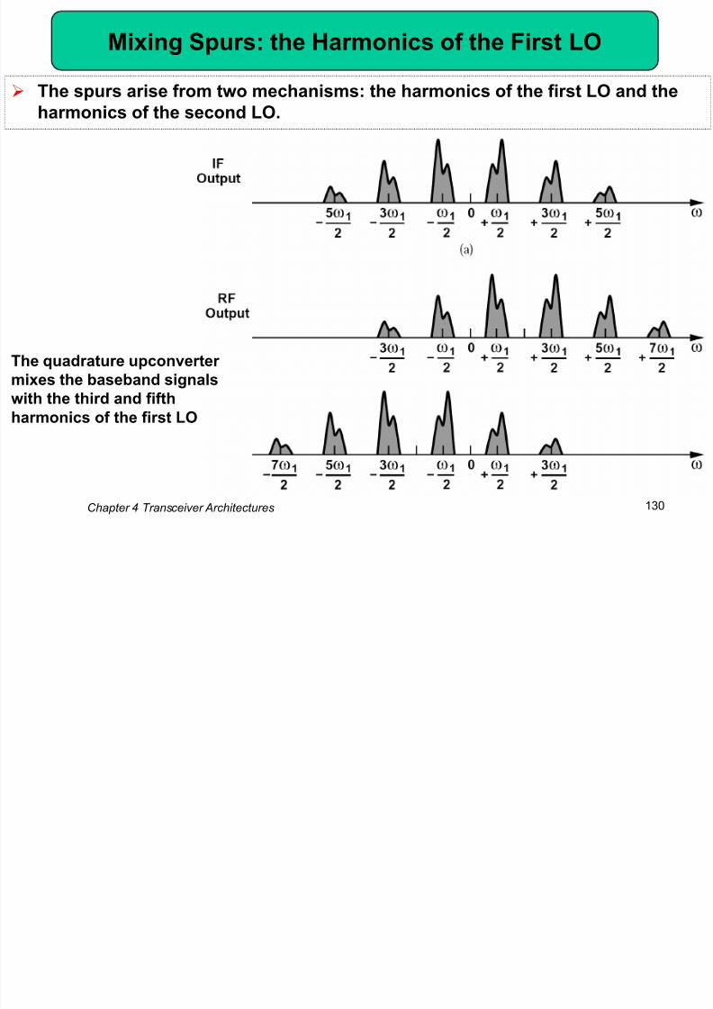
Mixing Spurs: the Harmonics of the First LO
Th i f t h i th h i f th fi t LO d th
8/12/2019 Chapter4 Transceiver Architectures
http://slidepdf.com/reader/full/chapter4-transceiver-architectures 130/137
Chapter 4 Transceiver Architectures 130
The spurs arise from two mechanisms: the harmonics of the first LO and the
harmonics of the second LO.
The quadrature upconverter
mixes the baseband signals
with the third and fifth
harmonics of the first LO
Mixing Spurs: the Harmonics of the Second LO
Th d h i l t t th h i f th d LO Th t i th
8/12/2019 Chapter4 Transceiver Architectures
http://slidepdf.com/reader/full/chapter4-transceiver-architectures 131/137
Chapter 4 Transceiver Architectures 131
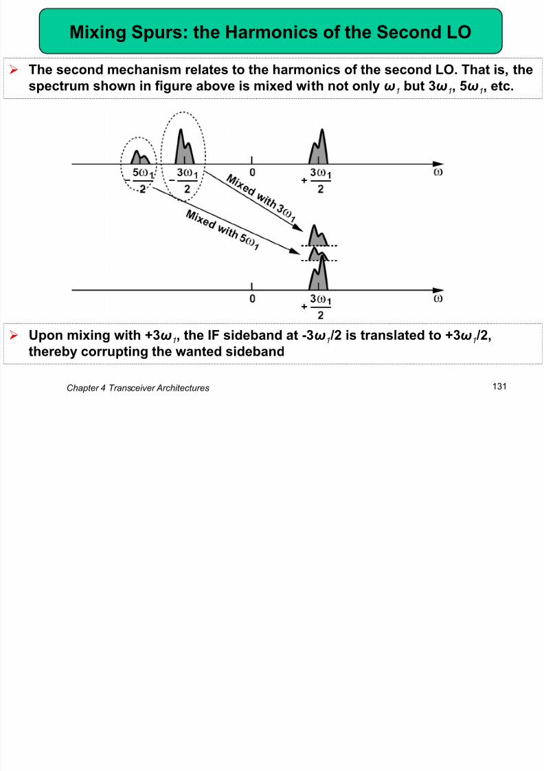
The second mechanism relates to the harmonics of the second LO. That is, the
spectrum shown in figure above is mixed with not only ω1 but 3ω1 , 5ω1 , etc.
Upon mixing with +3ω1 , the IF sideband at -3ω1 /2 is translated to +3ω1 /2,
thereby corrupting the wanted sideband
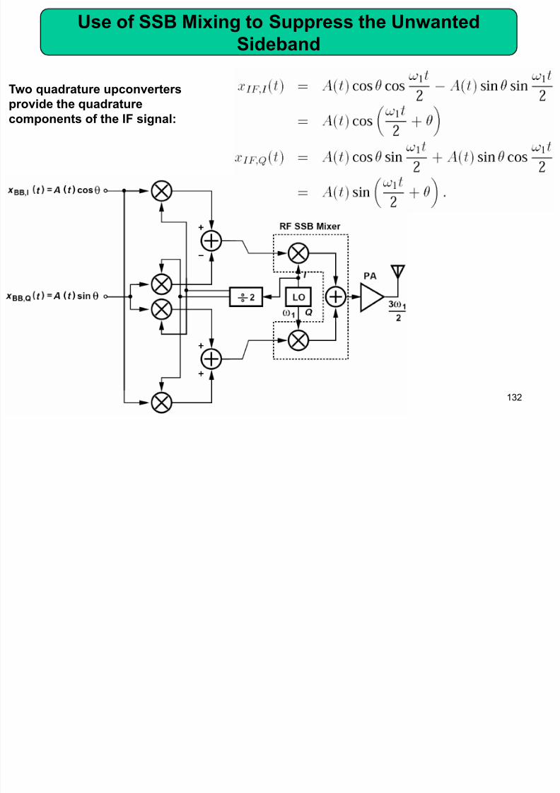
Use of SSB Mixing to Suppress the UnwantedSideband
8/12/2019 Chapter4 Transceiver Architectures
http://slidepdf.com/reader/full/chapter4-transceiver-architectures 132/137
Chapter 4 Transceiver Architectures 132
Two quadrature upconverters
provide the quadrature
components of the IF signal:
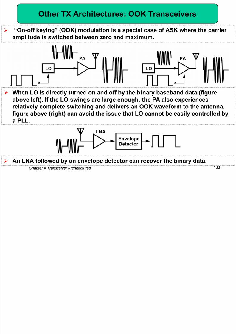
Other TX Architectures: OOK Transceivers
―O ff k i ‖ (OOK) d l ti i i l f ASK h th i
8/12/2019 Chapter4 Transceiver Architectures
http://slidepdf.com/reader/full/chapter4-transceiver-architectures 133/137
Chapter 4 Transceiver Architectures 133
―On-off keying‖ (OOK) modulation is a special case of ASK where the carrier
amplitude is switched between zero and maximum.
When LO is directly turned on and off by the binary baseband data (figure
above left), If the LO swings are large enough, the PA also experiences
relatively complete switching and delivers an OOK waveform to the antenna.
figure above (right) can avoid the issue that LO cannot be easily controlled by
a PLL.
An LNA followed by an envelope detector can recover the binary data.
References ( )

8/12/2019 Chapter4 Transceiver Architectures
http://slidepdf.com/reader/full/chapter4-transceiver-architectures 134/137
Chapter 4 Transceiver Architectures 134
References ( )
8/12/2019 Chapter4 Transceiver Architectures
http://slidepdf.com/reader/full/chapter4-transceiver-architectures 135/137
Chapter 4 Transceiver Architectures 135
References (Ⅲ)
8/12/2019 Chapter4 Transceiver Architectures
http://slidepdf.com/reader/full/chapter4-transceiver-architectures 136/137
Chapter 4 Transceiver Architectures 136
References (Ⅳ)
8/12/2019 Chapter4 Transceiver Architectures
http://slidepdf.com/reader/full/chapter4-transceiver-architectures 137/137