chapter cpus 2
TRANSCRIPT

CPUs 2CHAPTER POINTS
• Architectural mechanisms for embedded processors
• Parallelism in embedded CPU and GPUs
• Code compression and bus encoding
• Security mechanisms
• CPU simulation
• Configurable processors
2.1 IntroductionCPUs are at the heart of embedded systems. Whether we use one CPU or combineseveral CPUs to build a multiprocessor, instruction set execution provides the combi-nation of efficiency and generality that makes embedded computing powerful.
A number of CPUs have been designed especially for embedded applications oradapted from other uses. We can also use design tools to create CPUs to match thecharacteristics of our application. In either case, a variety of mechanisms can beused to match the CPU characteristics to the job at hand. Some of these mechanismsare borrowed from general-purpose computing; others have been developed especiallyfor embedded systems.
We will start with a brief introduction to the CPU design space. We will thenlook at the major categories of processors: RISC and DSPs in Section 2.3, andVLIW, superscalar, GPUs, and related methods in Section 2.4. Section 2.5 considersnovel variable-performance techniques such as better-than-worst-case design. InSection 2.6 we will study the design of memory hierarchies. Section 2.7 looks atthree topics that share similar mathematics: code compression, bus compression,and security. Section 2.8 surveys techniques for CPU simulation. Section 2.9 intro-duces some methodologies and techniques for the design of custom processors.
CHAPTER
59

2.2 Comparing processorsChoosing a CPU is one of the most important tasks faced by an embedded systemdesigner. Fortunately, designers have a wide range of processors to choose from,allowing them to closely match the CPU to the problem requirements. They caneven design their own CPU. In this section we will survey the range of processorsand their evaluation before looking at CPUs in more detail.
2.2.1 Evaluating processorsWe can judge processors in several ways. Many of these are metrics. Some evaluationcharacteristics are harder to quantify.
Performance is a key characteristic of processors. Different fields tend to use theterm “performance” in different waysdfor example, image processing tends to useperformance to mean image quality. Computer system designers use performanceto mean the rate at which programs execute.
We may look at computer performance more microscopically, in terms of a win-dow of a few instructions, or macroscopically over large programs. In the microscopicview, we may consider either latency or throughput. Figure 2.1 is a simple pipelinediagram that shows the execution of several instructions. In the figure, latency refersto the time required to execute an instruction from start to finish, while throughputrefers to the rate at which instructions are finished. Even if it takes several clock cyclesto execute an instruction, the processor may still be able to finish one instructionper cycle.
At the program level, computer architects also speak of average performance orpeak performance. Peak performance is often calculated assuming that instructionthroughput proceeds at its maximum rate and all processor resources are fully utilized.There is no easy way to calculate average performance for most processors; it isgenerally measured by executing a set of benchmarks on sample data.
Latency
IF ID EX
IF ID EX
IF ID EX
IF ID EX
ThroughputAdd r , r , r1 32
Sub r , r , r4 65
Add r , r , r2 85
Add r , r , r3 84
FIGURE 2.1
Latency and throughput in instruction execution.
Performance
60 CHAPTER 2 CPUs

However, embedded system designers often talk of program performance in termsof worst-case (or sometimes best-case) performance. This is not simply a character-istic of the processor; it is determined for a particular program running on a given pro-cessor. As we will see in later chapters, it is generally determined by analysis becauseof the difficulty of determining an input set that can be used to cause the worst-caseexecution.
Cost is another important measure of processors. In this case, we mean the pur-chase price of the processor. In VLSI design, cost is often measured in terms of thechip are required to implement a processor, which is closely related to chip cost.
Energy and power are key characteristics of CPUs. In modern processors, energyand power consumption must be measured for a particular program and data for ac-curate results. Modern processors use a variety of techniques to manage energy con-sumption on the fly, meaning that simple models of energy consumption do notprovide accurate results.
There are other ways to evaluate processors that are harder to measure. Predict-ability is an important characteristic for embedded systemsdwhen designing real-time systems we want to be able to predict execution time. Because predictabilityis affected by so many characteristics, ranging from the pipeline to the memory sys-tem, it is difficult to come up with a simple model for predictability.
Security is also an important characteristic of all processors, including embeddedprocessors. Security is inherently unmeasurable since the fact that we do not know ofa successful attack on a system does not mean that such an attack cannot exist.
2.2.2 A Taxonomy of processorsWe can classify processors in several dimensions. These dimensions interact somewhat,but they help us to choose a processor type based upon our problem characteristics.
Flynn [Fly72] created a well-known taxonomy of processors. He classifies proces-sors along two axes: the amount of data being processed and the number of instruc-tions being executed. This produces several categories:
• Single instruction, single data (SISD). This is more commonly known today as aRISC processor. A single stream of instructions operates on a single set of data.
• Single instruction, multiple data (SIMD). Several processing elements eachhave their own data, such as registers. However, they all perform the same oper-ations on their data in lockstep. A single program counter can be used to describeexecution of all the processing elements.
• Multiple instruction, multiple data (MIMD). Several processing elements havetheir own data and their own program counters. The programs do not have to run inlockstep.
• Multiple instruction, single data (MISD). Few, if any commercial computers fitthis category.
Instruction set style is one basic characteristic. The reduced instruction set com-puter (RISC)/complex instruction set computer (CISC) divide is well known.
Cost
Energy/power
Nonmetric
characteristics
Flynn’s categories
RISC vs. CISC
2.2 Comparing processors 61

The origins of this dichotomy were related to performancedRISC processors weredevised to make processors more easily pipelineable, increasing their throughput.However, instruction set style also has implications for code size, which can be impor-tant for cost and sometimes performance and power consumption as well (throughcache utilization). CISC instruction sets tend to give smaller programs than RISCand tightly encoded instruction sets still exist on some processors that are destinedfor applications that need small object code.
Instruction issue width is an important aspect of processor performance.Processors that can issue more than one instruction per cycle generally executeprograms faster. They do so at the cost of increased power consumption and highercost.
A closely related characteristic is how instructions are issued. Static scheduling ofinstructions is determined when the program is written. In contrast, dynamic sched-uling determines what instructions are issued at runtime. Dynamically scheduled in-struction issue allows the processor to take data-dependent behavior into accountwhen choosing how to issue instructions. Superscalar is a common technique for dy-namic instruction issue. Dynamic scheduling generally requires a much more com-plex and costly processor than static scheduling.
Instruction issue width and scheduling mechanisms are only one way to provideparallelism. Many other mechanisms have been developed to provide new types ofparallelism and concurrency. Vector processing uses instructions that generallyperform operations common in linear algebra on one- or two-dimensional arrays.Multithreading is a fine-grained concurrency mechanism that allows the processorto quickly switch between several threads of execution.
2.2.3 Embedded vs. general-purpose processorsGeneral-purpose processors are just thatdthey are designed to work well in a varietyof contexts. Embedded processors must be flexible, but they can often be tuned to aparticular application. As a result, some of the design precepts that are commonly fol-lowed in the design of general-purpose CPUs do not hold for embedded computers.And given the large number of embedded computers sold each year, many applicationareas make it worthwhile to spend the time to create a customized architecture. Notonly are billions of 8-bit processors sold each year, but hundreds of millions of32-bit processors are sold for embedded applications. Cell phones alone representthe largest single application of 32-bit CPUs.
One tenet of RISC design is single-cycle instructionsdan instruction spends oneclock cycle in each pipeline stage. This ensures that other stages do not stall whilewaiting for an instruction to finish in one stage. However, the most fundamentalgoal of processor design is application performance, which can be obtained by a num-ber of means.
One of the consequences of the emphasis on pipelining in RISC is simplified in-struction formats that are easy to decode in a single cycle. However, simple instructionformats result in increased code size. The Intel Architecture has a large number of
Single issue vs. multiple
issue
Static vs. dynamic
scheduling
Vectors, threads
RISC vs. embedded
62 CHAPTER 2 CPUs

CISC-style instructions with reduced numbers of operands and tight operation coding.Intel Architecture code is among the smallest code available when generated by agood compiler. Code size can affect performancedlarger programs make less effi-cient use of the cache.
2.3 RISC processors and digital signal processorsIn this section wewill look at the workhorses of embedded computing, RISC and DSP.Our goal is not to exhaustively describe any particular embedded processor; that taskis best left to data sheets and manuals. Instead, we will try to describe some importantaspects of these processors, compare and contrast RISC and DSP approaches to CPUarchitecture, and consider the different emphases of general-purpose and embeddedprocessors.
2.3.1 RISC processorsThe ARM architecture is supported by several families [ARM13]. The ARM Cortex-A family uses pipelines of up to 13 stages with branch prediction. A system caninclude from one to four cores with full L1 cache coherency and cache snooping. Itincludes the NEON 128-bit SIMD engine for multimedia functions, Jazelle Java Vir-tual Machine (JVM) acceleration, and a floating-point unit. The CORTEX-R family isdesigned for predictable performance. A range of interrupt interfaces and controllersallow designers to optimize the I/O structure for response time and features. Long in-structions can be stopped and restarted. A tightly coupled memory interface improveslocal memory performance. The Cortex-M family is designed for low-power opera-tion and deterministic behavior. The SecurCore processor family is designed for smartcards.
The MIPS architecture [MIP13] includes several families. The MIPS32 24Kfamily has an 8-stage pipeline; the 24KE includes features for DSP enhancements.The MIPS32 1074K core provides coherent multiprocessing and out-of-order super-scalar processing. Several cores provide accelerators: PowerVR provides support forgraphics, video, and display functions; Ensigma provides communicationsfunctions.
The Power Architecture [Fre07] is used in embedded and other computingdomains and encompasses architecture and tools. A base category of specificationsdefines the basic instruction set; embedded and server categories define mutuallyexclusive features added to the base features. The embedded category provides forseveral features: the ability to lock locations into the cache to reduce access time var-iations; enhanced debugging and performance monitoring; some memory manage-ment unit (MMU) features; processor control for cache coherency; and process IDsfor cache management. The AltiVec vector processor architecture is used in somehigh-performance Power Architecture processors. The signal processing engine(SPE) is a SIMD instruction set for accelerating signal processing operations. The
ARM
MIPS
Power Architecture
2.3 RISC processors and digital signal processors 63

variable-length encoding (VLE) category provides for alternate encodings of instruc-tions using a variable-length format.
The Intel Atom family [Int10, Int12] is designed for mobile and low-power appli-cations. Atom is based on the Intel Architecture instruction set. Family memberssupport a variety of features: virtualization technology, hyper-threading, design tech-niques that provide low-power operation, and thermal management.
2.3.2 Digital signal processorsToday, the term digital signal processor (DSP1) is often used as a marketing term.However, its original technical meaning still has some utility today. The AT&TDSP-16 [Bod80] was the first DSP. As illustrated in Figure 2.2, it introduced two fea-tures that define digital signal processors. First, it had an on-board multiplier and pro-vided a multiply-accumulate instruction. At the time the DSP-16 was designed,silicon was still very expensive and the inclusion of a multiplier was a major architec-tural decision. The multiply-accumulate instruction computes dest ¼ src1 * src2 þsrc3, a common operation in digital signal processing. Defining the multiply-accumulate instruction made the hardware somewhat more efficient because it elim-inated a register, improved code density by combining two operations into a singleinstruction, and improved performance. The DSP-16 also used a Harvard architecture
Instruction memory
Data memory
PC
IRControl
Registers
* +
FIGURE 2.2
A digital signal processor with a multiply-accumulate unit and harvard architecture.
Intel Atom
1Unfortunately, the literature uses DSP to mean both digital signal processor (a machine) and digitalsignal processing (a branch of mathematics).
64 CHAPTER 2 CPUs

with separate data and instruction memory. The Harvard structure meant that data ac-cesses could rely on consistent bandwidth from the memory, which is particularlyimportant for sampled-data systems.
Some of the trends evident in RISC architectures have also made their way intodigital signal processors. For example, high-performance DSPs have very deep pipe-lines to support high clock rates. There are major differences between modern proces-sors used in digital signal processing and those used for other applications in bothregister organization and opcodes. RISC processors generally have large, regular reg-ister files, which help simplify pipeline design as well as programming. Many DSPs,in contrast, have smaller general-purpose register files and many instructions thatmust use only one or a few selected registers. The accumulator is still a commonfeature of DSP architectures and other types of instructions may require the use ofcertain registers as sources or destinations for data. DSPs also often support special-ized instructions for digital signal processing operations, such as multiply-accumulate, operations for Viterbi encoding/decoding, etc.
The next example studies a family of high-performance DSPs.
Example 2.1 The Texas Instruments C5x DSP FamilyThe C5x family [Tex01, Tex01B] is an architecture for high-performance signal processing. TheC5x supports several features:
• A 40-bit arithmetic unit, which may be interpreted as 32-bit values plus 8 guard bits forimproved rounding control. The ALU can also be split to perform on two 16-bit operands.
• A barrel shifter performs arbitrary shifts for the ALU.• A 17� 17 multiplier and adder can perform multiply-accumulate operations.• A comparison unit compares the high and low accumulator words to help accelerate Viterbi
encoding/decoding.• A single-cycle exponent encoder can be used for wide-dynamic-range arithmetic.• Two dedicated address generators.
The C5x includes a variety of registers:
• Status registers include flags for arithmetic results, processor status, etc.• Auxiliary registers are used to generate 16-bit addresses.• A temporary register can hold a multiplicand or a shift count.• A transition register is used for Viterbi operations.• The stack pointer holds the top of the system stack.• A circular buffer size register is used for circular buffers common in signal processing.• Block-repeat registers help implement block-repeat instructions.• Interrupt registers provide the interface to the interrupt system.
The C5x family defines a variety of addressing modes. Some of them include:
• ARn mode performs indirect addressing through the auxiliary registers.• DP mode performs direct addressing from the DP register.• K23 mode uses an absolute address.• Bit instructions provide bit-mode addressing.
The RPT instruction provides single-instruction loops. The instruction provides a repeatcount that determines the number of times the following instruction is executed. Special reg-isters control the execution of the loop.
2.3 RISC processors and digital signal processors 65

The C5x family includes several implementations. The C54x is a lower-performance imple-mentation while the C55x is a higher-performance implementation.
The C54x pipeline has six stages:
• The prefetch program sends the PC value on the program bus.• Fetch loads the instruction.• The decode stage decodes the instruction.• The access step puts operand addresses on the buses.• The read step gets the operand values from the bus.• The execute step performs the operations.
The C55x microarchitecture includes three data read and two data write buses in additionto the program read bus:
3 data read buses
3 data read address buses
Program address bus
Program read bus32
2 data write buses
2 data write address buses
16
24
Instruction unit
Program flow unit
Address unit
Data unit
16
24
24
The C55x pipeline is longer than that of the C54x and it has a more complex structure. It isdivided into two stages:
Fetch Execute
4 7–8
The fetch stage takes four clock cycles; the execute stage takes seven or eight cycles.During fetch, the prefetch 1 stage sends an address to memory, while prefetch 2 waits for
the response. The fetch stage gets the instruction. Finally, the predecode stage sets updecoding.
During execution, the decode stage decodes a single instruction or instruction pair. Theaddress stage performs address calculations. Data access stages send data addresses to mem-ory. The read cycle gets the data values from the bus. The execute stage performs operationsand writes registers. Finally, the W and Wþ stages write values to memory.
The C55x includes 3 computation units and 14 operators. In general, the machine canexecute two instructions per cycle. However, some combinations of operations are not legaldue to resource constraints.
66 CHAPTER 2 CPUs

A co-processor is an execution unit that is controlled by the processor’s executionunit. (In contrast, an accelerator is controlled by registers and is not assigned opco-des.) Co-processors are used in both RISC processors and DSPs, but DSPs includesome particularly complex co-processors. Co-processors can be used to extend the in-struction set to implement common signal processing operations. In some cases, theinstructions provided by these co-processors can be integrated easily into other code.In other cases, the co-processor is designed to execute a particular stream of instruc-tions and the DSP acts as a sequencer for a complex, multicycle operation.
The next example looks at some co-processors for digital signal processing.
Example 2.2 TI C55x Co-processorThe C55x provides three co-processors for use in image processing and video compression: onefor pixel interpolation, one for motion estimation, and one for DCT/IDCT computation.
The pixel interpolation co-processor supports half-pixel computations that are often usedin motion estimation. Given a set of four pixels A, B, C, and D, we want to compute the inter-mediate pixels U, M, and R:
A B
C D
U
M R
Two instructions support this task. One loads pixels and computes:
ACy = copr(K8,AC,Lmem)
K8 is a set of control bits. The other instruction loads pixels, computes, and stores:
ACy = copr(K8,ACx,Lmem) jj Lmem=ACz
The motion estimation co-processor is built around a stylized usage pattern. It supports fullsearch and three heuristic search algorithms: three step, four step, and four step with half-pixelrefinement. It can produce either onemotion vector for a 16x16macroblock or four motion vec-tors for four 8x8 blocks. The basic motion estimation instruction has the form
[ACx,ACy] = copr(K8,ACx,ACy,Xmem,Ymem,Coeff)
where ACx and ACy are the accumulated sum of differences, K8 is a set of control bits, and
Xmem and Ymem point to odd and even lines of the search window.The DCT co-processor implements functions for one-dimensional DCT and IDCT computa-
tion. The unit is designed to support 8x8 DCT/IDCT and a particular sequence of instructionsmust be used to ensure that data operands are available at the required times. The co-processor
2.3 RISC processors and digital signal processors 67
provides three types of instructions: load, compute, and transfer to accumulators; compute,transfer and write to memory; and special.
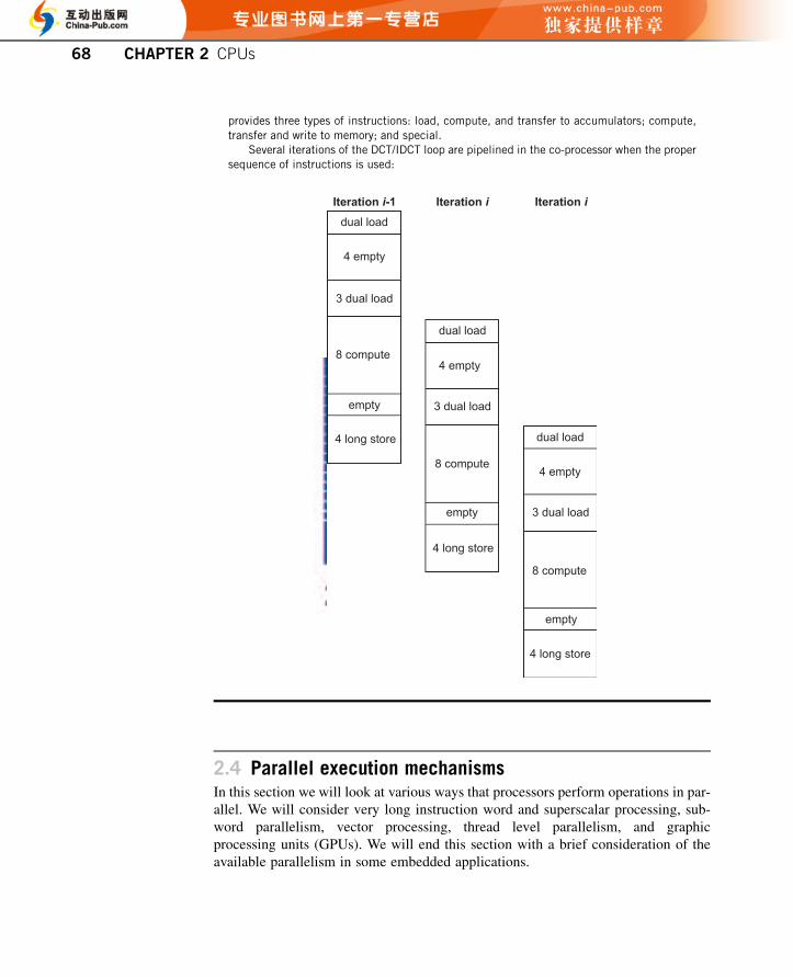
Several iterations of the DCT/IDCT loop are pipelined in the co-processor when the propersequence of instructions is used:
Iteration i-1 Iteration i Iteration idual load
dual load
dual load
3 dual load
3 dual load
3 dual load
4 empty
4 empty
4 empty
8 compute
8 compute
8 compute
empty
empty
empty
4 long store
4 long store
4 long store
2.4 Parallel execution mechanismsIn this section we will look at various ways that processors perform operations in par-allel. We will consider very long instruction word and superscalar processing, sub-word parallelism, vector processing, thread level parallelism, and graphicprocessing units (GPUs). We will end this section with a brief consideration of theavailable parallelism in some embedded applications.
68 CHAPTER 2 CPUs

2.4.1 Very long instruction word processorsVery long instruction word (VLIW) architectures were originally developed asgeneral-purpose processors but have seen widespread use in embedded systems.VLIWarchitectures provide instruction-level parallelism with relatively low hardwareoverhead.
Figure 2.3 shows a simplified version of a VLIW processor to introduce the basicprinciples of the technique. The execution unit includes a pool of function units con-nected to a large register file. Using today’s terminology for VLIW machines, theexecution unit reads a packet of instructionsdeach instruction in the packet can con-trol one of the function units in the machine. In an ideal VLIW machine, all instruc-tions in the packet are executed simultaneously; in modern machines, it may takeseveral cycles to retire all the instructions in the packet. Unlike a superscalar proces-sor, the order of execution is determined by the structure of the code and how instruc-tions are grouped into packets; the next packet will not begin execution until all theinstructions in the current packet have finished.
Because the organization of instructions into packets determines the scheduleof execution, VLIW machines rely on powerful compilers to identify parallelismand schedule instructions. The compiler is responsible for enforcing resourcelimitations and their associated scheduling policies. In compensation, theexecution unit is simpler because it does not have to check for many resourceinterdependencies.
The ideal VLIW is relatively easy to program because of its large, uniform registerfile. The register file provides a communication mechanism between the functionunits since each function unit can read operands from and write results to any registerin the register file.
Unfortunately, it is difficult to build large, fast register files with many ports. Asa result, many modern VLIW machines use partitioned register files as shown in
Control
Instruction 1 Instruction 2 Instruction n
Register file
Control
Instruction 1 Instruction 2 Instruction n
Register file
FIGURE 2.3
Structure of a generic VLIW processor.
VLIW basics
Split register files
2.4 Parallel execution mechanisms 69

Figure 2.4. In the example, the registers have been split into two register files, eachof which is connected to two function units. The combination of a register file and itsassociated function units is sometimes called a cluster. A cluster bus can be used tomove values between the register files. Register file to register file movement is per-formed under program control using explicit instructions. As a result, partitionedregister files make the compiler’s job more difficult. The compiler must partitionvalues among the register files, determine when a value needs to be copied fromone register file to another, generate the required move instructions, and adjustthe schedules of the other operations to wait for the values to appear. However,the characteristics of VLIW circuits often require us to design partitioned registerfile architectures.
VLIW machines have been used in applications with a great deal of data paral-lelism. The Trimedia family of processors, for example, was designed for use in videosystems. Video algorithms often perform similar operations on several pixels at time,making it relatively easy to generate parallel code. VLIW machines have also beenused for signal processing and networking. Cell phone baseband systems, forexample, must perform the same signal processing on many channels in parallel;the same instructions can be performed on separate data streams using VLIW archi-tectures. Similarly, networking systems must perform the same or similar operationson several packets at the same time.
The next example describes a VLIW digital signal processor.
Example 2.3 Texas Instruments C6000 VLIW DSPThe TI C6000 family [Tex11] is a VLIW architecture designed for digital signal processing. Thearchitecture is designed around a pair of data paths, each with its own 32-word register file(known as register files A and B). Each datapath has a .D unit for data load/store operations,a .L unit for logic and arithmetic, a .S unit for shift/branch/compare operations, and a .Munit for operations. These function units can all operate independently. They are supportedby a program bus that can fetch eight 32-bit instructions on every cycle and two data busesthat allow the .D1 and .D2 units to both fetch from the level 1 data memory on every cycle.
Cluster bus
Register file 1 Register file 2
FIGURE 2.4
Split register files in a VLIW machine.
Uses of VLIW
70 CHAPTER 2 CPUs

2.4.2 Superscalar processorsSuperscalar processors issue more than one instruction per clock cycle. Unlike VLIWprocessors, they check for resource conflicts on the fly to determine what combina-tions of instructions can be issued at each step. Superscalar architectures dominatedesktop and server architectures. Superscalar processors are not as common in theembedded world as in the desktop/server world. Embedded computing architecturesare more likely to be judged by metrics such as operations per watt rather than rawperformance.
A surprising number of embedded processors do, however, make use of supersca-lar instruction issue, though not as aggressively as do high-end servers. The embeddedPentium processor is a two-issue, in-order processor. It has two pipes: one for anyinteger operation and another for simple integer operations. We saw in Section2.3.1 that other embedded processors also use superscalar techniques.
2.4.3 SIMD and vector processorsMany applications present data-level parallelism that lends itself to efficientcomputing structures. Furthermore, much of this data is relatively small, which allowsus to build more parallel processing units to soak up more of that availableparallelism.
A variety of studies have shown that many of the variables used in most programshave small dynamic ranges. Figure 2.5 shows the results of one such study by Fritts[Fri00]. He analyzed the data types of programs in the MediaBench benchmark suite[Lee97]. The results show that 8-bit (byte) and 16-bit (half-word) operands dominatethis suite of programs. If we match the function unit widths to the operand sizes, wecan put more function units in the available silicon than if we simply used wide-wordfunction units to perform all operations.
100
80
60
40
Rat
io o
f dat
a ty
pes
(%)
20
0
Video
Imag
eGrap
hics
Audio
Speec
hSec
urity
Decod
e
Encod
eAve
rage
Floating-point Pointers Word Half-word
Media type
Byte
FIGURE 2.5
Operand sizes in mediabench benchmarks [Fri00].
Data operand sizes
2.4 Parallel execution mechanisms 71

One technique that exploits small operand sizes is subword parallelism [Lee94].The processor’s ALU can either operate in normal mode or it can be split into severalsmaller ALUs. An ALU can easily be split by breaking the carry chain so that bitslices operate independently. Each subword can operate on independent data; the op-erations are all controlled by the same opcode. Because the same instruction is per-formed on several data values, this technique is often referred to as a form of SIMD.
Another technique for data parallelism is vector processing. Vector processorshave been used in scientific computers for decades; they use specialized instructionsthat are designed to efficiently perform operations such as dot products on vectors ofvalues. Vector processing does not rely on small data values, but vectors of smallerdata types can perform more operations in parallel on available hardware, particularlywhen subword parallelism methods are used to manage datapath resources.
The next example describes a widely used vector processing architecture.
Example 2.4 AltiVec Vector ArchitectureThe AltiVec vector architecture [Ful98, Fre13] was defined by Motorola (now Freescale Semi-conductor) for the PowerPC architecture. AltiVec provides a 128-bit vector unit that can bedivided into operands of several sizes: 4 operands of 32 bits, 8 operands of 16 bits, or 16 op-erands of 8 bits. A register file provides 32 128-bit vectors to the vector unit. The architecturedefines a number of operations, including logical and arithmetic operands within an element aswell as interelement operations such as permutations.
2.4.4 Thread-level parallelismProcessors can also exploit thread- or task-level parallelism. It may be easier to findthread-level parallelism, particularly in embedded applications. The behavior ofthreads may be more predictable than instruction-level parallelism.
Multithreading architectures must provide separate registers for each thread. Butbecause switching between threads is stylized, the control required for multithreadingis relatively straightforward. Hardware multithreading alternately fetches instruc-tions from separate threads. On one cycle, it will fetch several instructions fromone thread, fetching enough instructions to be able to keep the pipelines full in theabsence of interlocks. On the next cycle, it fetches instructions from another thread.Simultaneous multithreading (SMT) fetches instructions from several threads oneach cycle rather than alternating between threads.
The Intel Atom S1200 [Int12] provides hyper-threading that allows the core to actas two logical processors. Each logical processor has its own set of general purposeand control registers. The underlying physical resourcesdexecution units, buses,and cachesdare shared.
2.4.5 GPUsGraphic processing units (GPUs) are widely used in PCs to perform graphics oper-ations. The most basic mode of operation in a GPU is SIMD. As illustrated in
Subword parallelism
Vectorization
Varieties of
multithreading
Multithreading in Atom
72 CHAPTER 2 CPUs

Figure 2.6, the graphics frame buffer holds the pixel values to be written onto thescreen. Many graphics algorithms perform identical operations on each section ofthe screen, with only the data changing by position in the frame buffer. The processingelements (PEs) for the GPU can be mapped onto sections of the screen. Each PE canexecute the same graphics code on its own data stream. The sections of the screen aretherefore rendered in parallel.
As mobile multimedia devices have proliferated, GPUs have migrated ontoembedded systems-on-chips. For example, the BCM2835 includes both an ARM11CPU and two VideoCore IV GPUs [Bro13]. The BCM2835 is used in the RaspberryPi embedded computer [Ras13].
The NVIDIA Fermi [NVI09] illustrates some important aspects of modernGPUs. Although it is not deployed on embedded processors at the time of thiswriting, we can expect embedded GPUs to embody more of these features asMoore’s Law advances. Figure 2.7 illustrates the overall Fermi architecture. Atthe center are three types of processing units: cores, load/store units, and specialfunction units that provide transcendental mathematical functions. The operationof all three units is controlled by the two warp schedulers and dispatch units. Awarp is a group of 32 parallel threads. One warp scheduler and dispatch unit cancontrol the execution of these two parallel threads across the cores, load/store,and special function units. Each warp scheduler’s warp is independent, so the twoactive warps execute independently. Physically, the system provides a registerfile, shared memory and L1 cache, and a uniform cache. Figure 2.8 shows the archi-tecture of a single core. Each core includes floating-point and integer units. Thedispatch port, operand collector, and result queue manage the retrieval of operandsand storage of results.
The programming model provides a hierarchy of programming units. Themost basic is the thread, identified by a thread ID. Each thread has its own pro-gram counter, registers, private memory, and inputs and outputs. A thread block,identified by its block ID, is a set of threads that share memory and can coor-dinate using barrier synchronization. A grid is an array of thread blocks thatexecute the same kernel. The thread blocks in a grid can share results usingglobal memory.
PE PE PE
PEPEPE
GPU
frame buffer screen
FIGURE 2.6
SIMD processing for graphics.
2.4 Parallel execution mechanisms 73

2.4.6 Processor resource utilizationThe choice of processor architecture depends in part on the characteristics of the pro-grams to be run on the processor. In many embedded applications we can leverage ourknowledge of the core algorithms to choose effective CPU architectures. However, wemust be careful to understand the characteristics of those applications. As an example,
instruction cache
warp scheduler/ dispatch
warp scheduler/dispatch
register file
cores load/ stores
special function
units
interconnection network
shared memory/L1 cache
uniform cache
FIGURE 2.7
The Fermi architecture.
dispatch port
operand collector
floating point unit integer unit
result queue
FIGURE 2.8
Architecture of a CUDA core.
74 CHAPTER 2 CPUs

many researchers assume that multimedia algorithms exhibit embarrassing levels ofparallelism. Experiments show that this is not necessarily the case.
Tallu et al. [Tal03] evaluated the instruction-level parallelism available inmultimedia applications. As shown in Figure 2.9, they evaluated several differentprocessor configurations using SimpleScalar. They measured nine benchmark pro-grams on the various architectures. The bar graphs show the instructions per cyclefor each application; most applications exhibit fewer than four instructionsper cycle.
Fritts [Fri00] studied the characteristics of loops in the MediaBench suite [Lee97].Figure 2.10 shows two measurements; in each case, results are shown with the bench-mark programs grouped into categories based on their primary function. The firstmeasurement shows the average number of iterations of a loop; fortunately, loopson average are executed many times. The second measurement shows path ratio,which is defined as
PR ¼ number of loop body instructions executed
total number of instructions in loop body� 100 (EQ 2.1)
Parameters
Feich width, decode width, issue width, and common widthRUU sizeLoad store queue Integer ALUs (latency/recovery = 1/J)Integer multipliers (latency/recovery = 3/I)Load store ports (latency/recovery = 1/J)L1 I-cache (size in KB, bit time, associativity, block size in bytes)L1 D-cache (size in KB, bit time, associativity, block size in bytes)L2 unified cache (size in KB, bit time, associativity, block size)Main memory widthMain memory latency (first chunk, next chunk)Branch predicator-bimodal (size, BTH size)
2-way 4-way 8-way 16-way2
221
32321664
64128
128256
4
4
24
4
8
88
8
16
16
1616,1,4,32 16,1,4,32 16,1,4,32
16,1,4,32 16,1,4,3216,1,4,3216,1,4,3232,1,4,64
256,6,4,64 256,6,4,64 256,6,4,64 256,6,4,6464 bits 128 bits 256 bits 256 bits65, 4 65, 4 65, 4 65, 42K, 2K 2K, 2K 2K, 2K 2K, 2K
224
48
816
1
Processor configurations
6
4
20
CFA
CFA
DCT
DCT
MOT
MOT
Scale
Scale
AUD
AUD
G711 JPEG IJPEG
G711 JPEG IJPEG
DECRYPT
DECRYPT
2-way 4-way
4-way
8-way
8-way
16-way
16-way
<1% <1% <1%
<1%
<1% <1% <1% <1% <1% <1% <1%
<1%
<1%<1%<1%<1%
<1%<1%
<4%<2%
<3% <1% <1%<1%
<1%
<1%
<1%
Results
IPC
SIMD ALUsSIMD Multipliers
FIGURE 2.9
An evaluation of the available parallelism in multimedia applications [Tal03] ©2003 IEEE.
Measurements on
multimedia benchmarks
2.4 Parallel execution mechanisms 75

Path ratio measures the percentage of a loop’s instructions that are actuallyexecuted. The average path ratio over all the MediaBench benchmarks was 78%,which means that 22% of the loop instructions were not executed.
These results should not be surprising given the nature of modern embedded algo-rithms. Modern signal processing algorithms have moved well beyond filtering. Manyalgorithms use control to improve performance. The large specifications for multi-media standards will naturally result in complex programs.
To take advantage of the available parallelism in multimedia and other embeddedapplications, we need to match the processor architecture to the application character-istics. These experiments suggest that processor architectures must exploit parallelismat several levels of abstraction.
2.5 Variable-performance CPU architecturesBecause so many embedded systems must meet real-time deadlines, predictableexecution time is a critical feature of the components used in embedded systems.However, traditional computer architecture designs have emphasized average
Aver
age
num
ber o
f ite
ratio
ns
1000
100
1
1
0.8
0.6
0.4
0.2
0
Media typeNumber of iterations per loop
Vide
o
Imag
e
Gra
phics
Audi
o
Spee
ch
Secu
rity
Med
ian
Media typePath ratio
Vide
o
Imag
e
Gra
phics
Audi
o
Spee
ch
Secu
rity
Aver
age
10
Path
ratio
FIGURE 2.10
Dynamic behavior of loops in MediaBench [Fri00].
Multimedia algorithms
Implications for CPUs
76 CHAPTER 2 CPUs

performance over worst-case performance, producing processors that are fast onaverage but whose worst-case performance is hard to bound. This often leads to con-servative designs of both hardware (oversized caches, faster processors) and software(simplified coding and restricted use of instructions).
As both power consumption and reliability become even more important, newtechniques have been developed that make processor behavior even more complex.Those techniques are finding their way into embedded processors even though theymake designs harder to analyze. In this section we will survey two important devel-opments, dynamic voltage and frequency scaling and better-than-worst-case design.We will explore the implications of these features and how to use them to our advan-tage in later chapters.
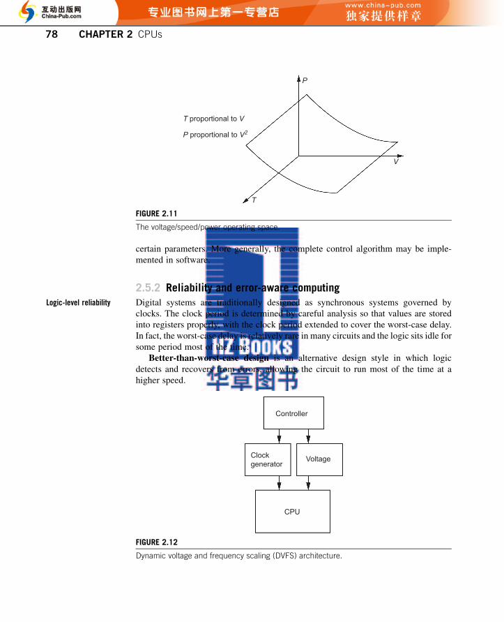
2.5.1 Dynamic voltage and frequency scalingDynamic voltage and frequency scaling (DVFS) [Wei94] is a popular technique forcontrolling CPU power consumption that takes advantage of the wide operating rangeof CMOS digital circuits.
Unlike many other digital circuit families, CMOS circuits can operate at a widerange of voltages [Wol02]. Furthermore, CMOS circuits operate more efficiently atlower voltages. The delay of a CMOS gate is a close to linear function of power supplyvoltage [Gon97]. The energy consumed during operation of the gate is proportional tothe square of the operating voltage:
E ¼ CV2 (EQ 2.2)
The speed-power product for CMOS (ignoring leakage) is also CV 2. Therefore, bylowering the power supply voltage, we can reduce energy consumption by V 2 whilereducing performance by only V.
Because we can operate CMOS logic at many different points, a CPU can be oper-ated within an envelope. Figure 2.11 illustrates the relationship between power supplyvoltage (V), operating speed (T), and power (P).
An architecture for dynamic voltage and frequency scaling operates the CPUwithin this space under a control algorithm. Figure 2.12 shows a DVFS architecture.The clock and power supply are generated by circuits that can supply a range ofvalues; these circuits generally operate at discrete points rather than continuouslyvarying values. Both the clock generator and voltage generator are operated by acontroller that determines when the clock frequency and voltage will change andby how much.
A DVFS controller must operate under constraints in order to optimize a designmetric. The constraints are related to clock speed and power supply voltage: notonly their minimum and maximum values, but how quickly clock speed or power sup-ply voltage can be changed. The design metric may be either to maximize perfor-mance given an energy budget or to minimize energy given a performance bound.
While it is possible to encode the control algorithm in hardware, the controlmethod is generally set at least in part by software. Registers may set the value of
DVFS
CMOS circuit
characteristics
DVFS architecture
DVFS control strategy
2.5 Variable-performance CPU architectures 77
certain parameters. More generally, the complete control algorithm may be imple-mented in software.
2.5.2 Reliability and error-aware computingDigital systems are traditionally designed as synchronous systems governed byclocks. The clock period is determined by careful analysis so that values are storedinto registers properly, with the clock period extended to cover the worst-case delay.In fact, the worst-case delay is relatively rare in many circuits and the logic sits idle forsome period most of the time.
Better-than-worst-case design is an alternative design style in which logicdetects and recovers from errors, allowing the circuit to run most of the time at ahigher speed.
T proportional to V
P proportional to V2
T
P
V
FIGURE 2.11
The voltage/speed/power operating space.
Controller
Clockgenerator
Voltage
CPU
FIGURE 2.12
Dynamic voltage and frequency scaling (DVFS) architecture.
Logic-level reliability
78 CHAPTER 2 CPUs

The Razor architecture [Ern03] is one architecture for better-than-worst-case per-formance. Razor uses a specialized register, shown in Figure 2.13, which measuresand evaluates errors. The system register holds the latched value and is clocked atthe higher-than-worst-case clock rate. A separate register is clocked separately andslightly behind the system register. If the results stored in the two registers aredifferent, then an error occurred, probably due to timing. The XOR gate measuresthat error and causes the later value to replace the value in the system register.
The Razor microarchitecture does not cause an erroneous operation to be recalcu-lated in the same stage. Rather, it forwards the operation to a later stage. This avoidshaving a stage with a systematic problem stall the pipeline with an indefinite numberof recalculations.
Hu et al. [Hu09] used a combination of architectural support and compiler en-hancements to support redundancy in VLIW processors. They duplicate instructionsand compare the results to check for transient errors. The compiler schedules twocopies of the instruction; a bit in the instruction identifies it as either an original ora duplicate. Queues hold the results of computations before either writing a registeror performing a load/store. Logic compares the original and duplicate values and flagsan error if necessary.
Many signal processing and control applications are tolerant of certain types oferrors. That tolerance can be exploited to reduce the energy consumption of logic cir-cuits: operating at low voltages changes the delays through gates, causing transienterrors in calculation, but also reducing the logic’s energy consumption. If the logicis not given enough settling time, the erroneous value is captured. Chakrapani et al.[Cha08] proposed a model for energy-accuracy trade-offs in CMOS. They observedthat errors in the low-order bits contribute less to error magnitude than do errors inhigh-order bits. They proposed dividing words into bins, each with a different powersupply voltage, depending on the contribution of the bits in that bin to total error. They
01
D
D
Q
Q
System clock
Razor clock
Error
FIGURE 2.13
A Razor latch.
Razor microarchitecture
VLIW error detection
Error-aware computing
2.5 Variable-performance CPU architectures 79

showed that this error-biased voltage scaling reduced error at a rate Uð2n=cÞ comparedto uniform voltage scaling where n is the number of bits per word and c is related tothe bin size.
Kim et al. [Kim11] argued that delay-induced error rates in adders depend not onlyon the current values but also the previous values. The delay along the adder’s criticalpath depends on whether a bit of the carry chain changes value, which depends onboth the previous and current values being added. They used simulation to showthat static error analysis overestimates errors. They also showed that ripple-carry ad-ders are less sensitive to delay-oriented errors than are Kogge-Stone adders and arraymultipliers; the ripple-carry adder has a single dominant critical path along the carrychain, while the Kogge-Stone and array multipliers have many subcritical paths thatcan be pushed into criticality with small changes to delay. They proposed adaptivetruncation as an effective method for energy savings with low quality degradationfor image compression [Kim10].
2.6 Processor memory hierarchyThe memory hierarchy is a critical determinant of overall system performance and po-wer consumption. In this section we will review some basic concepts in the design ofmemory hierarchies and how they can be exploited in the design of embedded proces-sors. We will start by introducing a basic model of memory components that we canuse to evaluate various hardware and software design strategies. We will then considerthe design of register files and caches. We will end with a discussion of scratch padmemory, which has been proposed as an adjunct to caches in embedded processors.
2.6.1 Memory component modelsIn order to evaluate some memory design methods, we need models for the physicalproperties of memory: area, delay, and energy consumption. Because a variety ofstructures at different levels of the memory hierarchy are built from the same compo-nents, we can use a single model throughout the memory hierarchy and for differenttypes of memory circuits.
Figure 2.14 shows a generic structural model for a two-dimensional memoryblock. This model does not depend on the details of the memory circuit and so appliesto various types of dynamic RAM, static RAM, and read-only memory. The basic unitof storage is the memory cell. Cells are arranged in a two-dimensional array. Thismemory model describes the relationships between the cells and their associatedaccess circuitry.
Within the memory core, cells are connected to row and bit lines that provide atwo-dimensional addressing structure. The row line selects a one-dimensional rowof cells, which then can be accessed (read or written) via their bit lines. When arow is selected, all the cells in that row are active. In general, there may be morethan one bit line, since many memory circuits use both the true and complement formsof the bit.
Transition-based error
analysis
Memory block structure
80 CHAPTER 2 CPUs

The row decoder circuitry is a demultiplexer that drives one of the n row lines inthe core by decoding the r bits of row address. A column decoder selects a b-bit widesubset of the bit lines based upon the c bits of column address. Some memory alsorequires precharge circuits to control the bit lines.
The area model of the memory block has components for the elements of theblock model:
A ¼ Ar þ Ax þ Ap þ Ac (EQ 2.3)
The row decoder area is
Ar ¼ arn (EQ 2.4)
where ar is the area of a one-bit slice of the row decoder.The core area is
Ax ¼ axmn (EQ 2.5)
where ax is the area of a one-bit core cell, including its share of the row and bit lines.The precharge circuit area is
Ap ¼ apn (EQ 2.6)
where ap is the area of a one-bit slice of the precharge circuit.The column decoder area is
Ac ¼ acn (EQ 2.7)
where ac is the area of a one-bit slice of the column decoder.
Row decoder
Core
Precharge circuits
Columndecoder
Cell Row line
Bit line
a r
c
b
n
m
FIGURE 2.14
Structural model of a memory block.
Area model
2.6 Processor memory hierarchy 81
The delay model of the memory block follows the flow of information in a mem-ory access. Some of its elements are independent of m and n while others depend onthe length of the row or column lines in the cell:
D ¼ Dsetup þ Dr þ Dx þ Dbit þ Dc (EQ 2.8)
Dsetup is the time required for the precharge circuitry. It is generally independent of thenumber of columns, but may depend on the number of rows due to the time required toprecharge the bit line. Dr is the row decoder time, including the row line propagationtime. The delay through the decoding logic generally depends upon the value ofm, butthe dependence may vary due to the type of decoding circuit used. Dx is the reactiontime of the core cell itself. Dbit is the time required for the values to propagate throughthe bit line. Dc is the delay through the column decoder, which once again may dependon the value of n.
The energy model must include both static and dynamic components. Thedynamic component follows the structure of the block to determine the total energyconsumption for a memory access:
ED ¼ Er þ Ex þ Ep þ Ec (EQ 2.9)
given the energy consumptions of the row decoder, core, precharge circuits, and col-umn decoder. The core energy depends on the values of m and n due to the row and bitlines. The decoder circuitry energy also depends on m and n, though the details ofthose relationships depend on the circuits used.
The static component ES models the standby energy consumption of the memory.The details vary for different types of memory but the static component can besignificant.
The total energy consumption is
E ¼ ED þ ES (EQ 2.10)
This model describes single-port memory, in which a single read or write can beperformed at any given time. Multiport memory accepts multiple addresses/data forsimultaneous accesses. Some aspects of the memory block model extend easily tomultiport memory. However, delay for multiport memory is a nonlinear function ofthe number of ports. The exact relationship depends on the detail of the core circuitdesign, but the memory cell core circuits introduce nonlinear delay as ports are addedto the cell.
Figure 2.15 shows the results of one set of simulation experiments that measuredthe delay of multiport SRAM as a function of the number of ports and memory size[Dut98].
Energy models for caches are particularly important in CPU and program design.Kamble and Ghose [Kam97] developed an analytical model of power consumption incaches. Given an m-way set associative cache with a capacity of D bytes, a tag size of
Delay model
Energy model
Multiport memory
Cache models
82 CHAPTER 2 CPUs

T bits, and a line size of L bytes, with St status bits per block frame, they divide thecache energy consumption into several components:
• Bit line energy
Ebit ¼ 1
2V2DD
�Nbit;pr$Cbit;pr þ Nbit;r$Cbit; r
wþ Nbit;w$Cbit; r
w
þ mð8Lþ t þ StÞ$CA$�Cg;Qpa þ Cg;Qpb þ Cg;Qp
��(EQ 2.11)
where Nbit,pr, Nbit,r, and Nbit,w are the number of bit line transitions due to precharg-ing, reads, and writes, Cbit,pr and Cbit,rw are the capacitance of the bit lines duringprecharging and read/write operations, and CA is the number of cache accesses.
• Word line energy
Eword ¼ V2DD$CA$ð8Lþ t þ StÞ�2Cg;Q1 þ Cwordwire
�(EQ 2.12)
where Cg,Q1 is the gate capacitance of the access transistor for the bit line andCwordwire is the capacitance of the word line.
• Output line energyTotal output energy is divided into address and data line dissipation and may occurwhen driving lines either toward the CPU or toward memory. The N values are the
16
14
12
10
8
6
4
22 4 6 8 10 12 14 16
Memory size
Mem
ory
dela
y (n
s)
1 port 2 ports 4 ports 6 ports 8 ports
FIGURE 2.15
Memory delay as a function of number of ports [Dut98] ©1998 IEEE.
2.6 Processor memory hierarchy 83

number of transitions (d2m for data to memory, d2c for data to CPU, for example)and the C values are the corresponding capacitive loads:
Eaoutput ¼ 1
2V2DD
�Nout;azm$Cout;azm þ Nout;azc$Cout;azc
�(EQ 2.13)
Edoutput ¼ 1
2V2DD
�Nout;dzm$Cout;dzm þ Nout;dzc$Cout;dzc
�(EQ 2.14)
• Address input lines
Eainput ¼ 1
2V2DDNainput
�ðmþ 1Þ$2$S$Cin;dec þ Cawire
�(EQ 2.15)
where Nainput is the number of transitions in the address input lines, Cin,dec is thegate capacitance of the first decoder level, and Cawire is the capacitance of thewires that feed the RAM banks.
Kamble and Ghose developed formulas to derive the number of transitions invarious parts of the cache based upon the overall cache activity.
Shiue and Chakrabarti [Shi99] developed a simpler cache model that they showedgave results similar to Kamble and Ghose’s model. Their model used several defini-tions: add_bs is the number of transitions on the address bus per instruction; data_bsis the number of transitions on the data bus per instruction, word_line_size is the num-ber of memory cells on a word line, bit_line_size is the number of memory cells in abit line, Em is the energy consumption of a main memory access, and a, b, and g aretechnology parameters. The energy consumption is given by
Energy ¼ hit_rate � energy_hit þ miss_rate � energy_miss (EQ 2.16)
Energy_hit ¼ E_decþ E_cell (EQ 2.17)
Energy_miss ¼ E_decþ E_cellþ E_ioþ E_main
¼ Energy_hit þ E_ioþ E_main(EQ 2.18)
E_dec ¼ a � add_bs (EQ 2.19)
E_þ dell ¼ b � word_line_size � bit_line_size (EQ 2.20)
E_io ¼ g � ðdata_bs � cache-line_sizeþ add_bsÞ (EQ 2.21)
E_main ¼ g � data_bs � cache_line_sizeþ Em � cache_line_size (EQ 2.22)
We may also want to model the bus that connects the memory to the remainder ofthe system. Buses present large capacitive loads that introduce significant delay andenergy penalties.
Larger memory structures can be built from memory blocks. Figure 2.16 shows asimple wide memory in which several blocks are accessed in parallel from the sameaddress lines. A set-associative cache could be constructed from this array, forexample, by a multiplexer that selects the data from the block that corresponds to
Buses
Memory arrays
84 CHAPTER 2 CPUs

the appropriate set. Parallel memory systems may be built by feeding separate ad-dresses to different memory blocks.
Many architectures use a memory controller to mediate memory accesses fromthe CPU. Given the complexity of modern DRAM components, a memory controllercan maximize performance of the memory system by properly scheduling memoryaccesses. McKee et al. [McK00] proposed a combination of compile-time detectionof streams with runtime scheduling. Compile-time analysis determines the baseaddress, stride, and vector length of streams, and the controller architecture uses aset of FIFOs to store streams. A memory scheduling unit uses the stream parametersdetermined by the compiler along with knowledge of the memory architecture tomake scheduling decisions. Rixner et al. [Rix00] used a buffer per bank to holdpending references. Precharge and row arbiters manage those functions per bankand row. A column arbiter arbitrates among column accesses, while an address arbiterperforms the final selection of an operation. Their architecture supports severaldifferent scheduling policies for precharging and row and column arbitration. Leeet al. [Lee05] proposed a layered architecture that separates performance-orientedscheduling from low-level SDRAM operations such as refresh. They support threetypes of access channels. Latency-sensitive channels require fast response and aregiven the highest priority. Bandwidth-sensitive channels require bandwidth but arenot sensitive to latency. Don’t-care channels have the lowest priority.
Cho et al. [Cho09] proposed an accuracy-aware SRAMarchitecture formobilemulti-media. They observed that errors in low-order bits in image and video data cause lessnoticeable image/video distortion than do errors in high-order bits. They designed anSRAMarchitecture inwhich power supplyvoltage could bemodified columnbycolumn.They found that their architecture provided 20% higher power savings at the same imagequality degradation as compared to blind voltage scaling of all bits in the memory.
2.6.2 Register filesThe register file is the first stage of the memory hierarchy. Although the size of theregister file is fixed when the CPU is predesigned, if we design our own CPUs then
Address
Memory block
Memory block
b b
FIGURE 2.16
A memory array built from memory blocks.
Memory controllers
Accuracy-aware SRAM
2.6 Processor memory hierarchy 85
we can select the number of registers based upon the application requirements. Reg-ister file size is a key parameter in CPU design that affects code performance and en-ergy consumption as well as the area of the CPU.
Register files that are either too large or too small relative to the application’sneeds incur extra costs. If the register file is too small, the program must spill valuesto main memory: the value is written to main memory and later read back from mainmemory. Spills cost both time and energy because main memory accesses are slowerand more energy-intensive than register file accesses. If the register file is too large,then it consumes static energy as well as taking extra chip area that could be usedfor other purposes.
The most important parameters in register file design are the number of wordsand the number of ports. Word width affects register file area and energy consump-tion, but is not closely coupled to other design decisions. The number of words moredirectly determines area, energy, and performance. The number of ports is importantbecause, as noted before, delay is a nonlinear function of the number of ports. Thisnonlinear dependency is the key reason that many VLIW machines use partitionedregister files.
Wehmeyer et al. [Weh01] studied the effects of varying register file size on a pro-gram’s dynamic behavior. They compiled a number of benchmark programs and usedprofiling tools to analyze the program’s behavior. Figure 2.17 shows performance andenergy consumption as a function of register file size. In both cases, overly small reg-ister files result in nonlinear penalties whereas large register files present little benefit.
2.6.3 CachesCache design has received a lot of attention in general-purpose computer design. Mostof those lessons apply to embedded computers as well, but because we may design theCPU to meet the needs of a particular set of applications, we can pay extra attention tothe relationship between the cache configuration and the programs that will use it.
As with register files, caches have a sweet spot that is neither too small nortoo large. Li and Henkel [Li98] measured the influence of caches on energyconsumption in detail. Figure 2.18 shows the energy consumption of a CPUrunning an MPEG encoder. Energy consumption has a global minimum: too-small caches result in excessive main memory accesses; too-large caches consumeexcess static power.
The most basic cache parameter is total cache size. Larger caches can hold moredata or instructions at the cost of increased area and static power consumption. Givena fixed number of bits in the cache, we can vary both the set associativity and the linesize. Splitting a cache into more sets allows us to independently reference morelocations that map onto similar cache locations at the cost of mapping more memoryaddresses into a given cache line. Longer cache lines provide more prefetching band-width, which is useful in some algorithms but not others.
Line size affects prefetching behaviordprograms that access successivememory locations can benefit from the prefetching induced by long cache lines.
Sweet spot in register file
design
Register file parameters
Sweet spot in cache
design
Cache parameters and
behavior
Cache parameter
selection
86 CHAPTER 2 CPUs

Long lines may also in some cases provide reuse for very small sets of loca-tions. Set-associative caches are most effective for programs with large workingsets or working sets made of several disjoint sections.
Panda et al. [Pan99] developed an algorithm to explore the memory hierarchydesign space and to allocate program variables within the memory hierarchy. They
3
2.5
2
1.5
1
0.5
03 4 5 6 7 8
Number of registers Performance vs. number of registers
0.035
0.03
0.025
0.02
0.015
0.01
0.005
03 4 5 6 7 8
Number of registersEnergy consumption vs. number of registers
biquad (x 650) lattice_init (x 1) matrix-mult (x 100)me_ivlin (x 1) bubble_sort (x 3) heap_sort (x 12)insertion_sort (x 5) selection_sort (x 6)
Ener
gy c
onsu
mpt
ion
(WS)
Num
ber o
f cyc
les
(mill
ions
)
FIGURE 2.17
Performance and energy consumption as a function of register file size [Weh01] ©2001 IEEE.
2.6 Processor memory hierarchy 87

allocated frequently used scalar variables to the register file. They used the classifica-tion of Wolfe and Lam [Wol91] to analyze the behavior of arrays:
• Self-temporal reuse means that the same array element is accessed in differentloop iterations.
• Self-spatial reuse means that the same cache line is accessed in different loopiterations.
• Group-temporal reuse means that different parts of the program access the samearray element.
• Group-spatial reuse means that different parts of the program access the samecache line.
This classification treats temporal reuse (the same data element) as a special caseof spatial reuse (the same cache line). Panda et al. divide memory references intoequivalence classes, with each class containing a set of references with self-spatialand group-spatial reuse. The equivalence classes allow them to estimate the numberof cache misses required by those references. They assume that spatial locality canresult in reuse if the number of memory references in the loop is less than the cachesize. Group-spatial locality is possible when a row fits into a cache and the other dataelements used in the loop are smaller than the cache size. Two sets of accesses arecompatible if their index expressions differ by a constant.
Energy [ ]joules
MPEG
1
0.1
9
910
1011
11121213
13141415 15
Dcache size[2** Val]Icache size[2** Val]
FIGURE 2.18
Energy consumption vs. instruction/data cache size for an MPEG benchmark program [Li98B]
©1998 ACM.
88 CHAPTER 2 CPUs

Gordon-Ross et al. [Gor04] developed a method to optimize multilevel cache hi-erarchies. They adjusted cache size, then line size, then associativity. They found thatthe configuration of the first-level cache affects the required configuration for thesecond-level cacheddifferent first-level configurations cause different elements tomiss the first-level cache, causing different behavior in the second-level cache.To take this effect into account, the alternately chose cache size for each level, thenline size for each level, and finally associativity for each level.
Several groups, such as Balasubramonian et al. [Bal03], have proposed configura-ble caches whose configuration can be changed at runtime. Additional multiplexersand other logic allow a pool of memory cells to be used in several different cache con-figurations. Registers hold the configuration values that control the configurationlogic. The cache has a configuration mode in which the cache parameters can beset; the cache acts normally in operation mode between configurations. The configu-ration logic incurs an area penalty as well as static and dynamic power consumptionpenalties. The configuration logic also increases the delay through the cache.However, it allows the cache configuration to be adjusted for different parts of the pro-gram in fairly small increments of time.
2.6.4 Scratch pad memoryA cache is designed to move a relatively small amount of memory close to the pro-cessor. Caches use hardwired algorithms to manage the cache contentsdhardware de-termines when values are added or removed from the cache. Software-orientedschemes are an alternative way to manage close-in memory.
As shown in Figure 2.19, scratch pad memory [Pan00] is located parallel to thecache. However, the scratch pad does not include hardware to manage its contents.
Main memory
Memory controllerCache hit
Cache
Scratch pad hit
Scratch pad
CPU
FIGURE 2.19
Scratch pad memory in a system.
Configurable caches
Scratch pads
2.6 Processor memory hierarchy 89

The CPU can address the scratch pad to read and write it directly. The scratch padappears in a fixed part of the processor’s address space, such as the lower range of ad-dresses. The scratch pad is sized to provide high-speed memory that will fit on-chip.The access time of a cache is predictable, unlike accesses to a cache. Predictability isthe key attribute of a scratch pad.
Because the scratch pad is part of the main memory space, standard read and writeinstructions can be used to manage the scratch pad. Management requires determiningwhat data is in the scratch pad and when it is removed from the cache. Software canmanage the cache using a combination of compile-time and runtime decision making.We will discuss management algorithms in more detail in Section 3.3.4.
2.7 Encoding and securityThis section covers two important topics in the design of embedded processors:encoding of instructions and data for efficiency and security architectures. We willstart with a discussion of algorithms to generate compressed representations of in-structions that can be dynamically decoded during execution. We will then expandthis discussion to include methods for combined code and data compression. Wewill then describe methods to encode bus traffic to reduce the power consumptionof address and data buses. We will end with a survey of security-related mechanismsin processors.
2.7.1 Code compressionCode compression is one way to reduce object code size. Compressed instruction setsare not designed by people, but rather by algorithms. We can design an instruction setfor a particular program, or we can use algorithms to design a program based on moregeneral program characteristics. Surprisingly, code compression can improve perfor-mance and energy consumption as well. As we saw previously, the Power Architec-ture provides support for variable-length instruction encodings.
The ARM Thumb instruction set [Slo04] is a manually designed compact instruc-tion set. It is an extension to the basic ARM instruction set; any implementation thatrecognizes Thumb instructions must also be able to interpret standard ARM instruc-tions. Thumb instructions are 16 bits long.
A series of studies have developed methods for the automatic generation of com-pressed instruction formats that are suitable for on-the-fly decompression duringexecution. Wolfe and Chanin [Wol92] proposed code compression and developedthe first method for executing compressed code. Relatively small modifications toboth the compilation process and the processor allow the machine to execute codethat has been compressed by lossless compression algorithms. Figure 2.20 shows theircompilation process. The compiler itself is not modified. The object code (or perhapsassembly code in text form) is fed into a compression program that uses losslesscompression to generate a new, compressed object file that is loaded into the
Synthesized compressed
code
90 CHAPTER 2 CPUs

processor’s memory. The compression program modifies the instruction but leavesdata intact. Because the compiler need not be modified, compressed code generationis relatively easy to implement.
Wolfe and Chanin used Huffman’s algorithm [Huf52] to compress code.Huffman’s algorithm was the first modern algorithm for code compression. It requiresan alphabet of symbols and the probabilities of occurrence of those symbols. Asshown in Figure 2.21, a coding tree is built based on those probabilities. Initially,we build a set of subtrees, each having only one leaf node for a symbol. The scoreof a subtree is the sum of the probabilities of all its leaf nodes. We repeatedly choosethe two lowest-score subtrees and combine them into a new subtree, with the lower-probability subtree taking the 0 branch and the higher-probability subtree taking the1 branch. We continue combining subtrees until we have formed a single large tree.The code for a symbol can be found by following the path from the root to the appro-priate leaf node, noting the encoding bit at each decision point.
Figure 2.22 shows the structure of a CPU modified to execute compressed codeusing the Wolfe and Chanin architecture. A decompression unit is added betweenthe main memory and the cache. The decompressor intercepts instruction reads(but not data reads) from the memory and decompresses instructions as they gointo the cache. The decompressor generates instructions in the CPU’s native instruc-tion set. The processor execution unit itself does not have to be modified because itdoes not see compressed instructions. The relatively small changes to the hardwaremake this scheme easy to implement with existing processors.
Source code Compiler Object
code Compressor Compressed object code
FIGURE 2.20
How to generate a compressed program.
abcdefgh
0.200.010.010.010.300.100.0960.300.01
Symbols and probabilities
00
00
0
0
11
11
1
1
0 1 0 1
c b d i g f a e h
.01 .01 .01 .01 .10 .20 .30 .30.096Coding tree
i
FIGURE 2.21
Huffman coding.
Huffman coding
Microarchitecture with
code decompression
2.7 Encoding and security 91

As illustrated in Figure 2.23, hand-designed instruction sets generally use a rela-tively small number of distinct instruction sizes and typically divide instructions onword or byte boundaries. Compressed instructions, in comparison, can be of arbitrarylength. Compressed instructions are generally generated in blocks. The compressedinstructions are packed bit by bit into blocks, but the blocks start on more naturalboundaries, such as bytes or words. This leaves empty space in the compressed pro-gram that is overhead for the compression process.
The block structure affects execution. The decompression engine decompressescode a block at a time. This means that several instructions become available in shortorder, although it generally takes several clock cycles to finish decompressing a block.Blocks effectively lengthen prefetch time.
Block structure also affects the compression process and the choice of a compres-sion algorithm. Lossless compression algorithms generally work best on long blocksof data. However, longer blocks impede efficient execution because programs are notexecuted sequentially from beginning to end. If the entire program were a singleblock, we would decompress the entire block before execution, which would nullifythe advantages of compression. If blocks are too short, the code will not be sufficientlycompressed to be worthwhile.
Memory Decompressor Cache Controller
Data path
FIGURE 2.22
The Wolfe/Chanin architecture for executing compressed code.
add r1,r2,r3
mov r1,a
bne r1,foo
Uncompressed Compressed
FIGURE 2.23
Compressed vs. uncompressed code.
Compressed code blocks
92 CHAPTER 2 CPUs

Figure 2.24 shows Wolfe and Chanin’s comparison of several compressionmethods. They compressed several benchmark programs in four different ways: usingthe UNIX compress utility; using standard Huffman encoding on 32-byte blocks ofinstructions; using a Huffman code designed specifically for that program; using abounded Huffman code, which ensures that no byte is coded in a symbol longerthan 16 bits, once again with a separate code for each program; and with a singlebounded Huffman code computed from several test programs and used for all thebenchmarks.
Wolfe and Chanin also evaluated the performance of their architecture on thebenchmarks using four different memory models: programs stored in EPROM with100 ns memory access time; programs stored in burst-mode EPROMwith three cyclesfor the first access and one cycle for subsequent sequential accesses; and static-column DRAM with four cycles for the first access and one cycle for subsequentsequential accesses, based on 70 ns access time. They found that system performanceimproved when compressed code was run from slow memory and that system perfor-mance slowed down about 10% when executed from fast memory.
If a branch is taken in the middle of a large block, we may not use some of theinstructions in the block, wasting the time and energy required to decompress thoseinstructions. As illustrated in Figure 2.25, branches and branch targets may be at arbi-trary points in blocks. The ideal size of a block is related to the distances betweenbranches and branch targets. Compression also affects jump tables and computedbranch tables [Lef97].
The locations of branch targets in the uncompressed code must be adjusted in thecompressed code because the absolute locations of all the instructions move as a resultof compression. Most instruction accesses are sequential, but branches may go to
100.0%
90.0%
80.0%
70.0%
60.0%
50.0%
40.0%
30.0%
20.0%
10.0%
0.0%lex53172 bytes
pswarp 61364 bytes
yacc49076bytes
who85940bytes
eightq4020 bytes
matrix25A36788 bytes
lloop014020 bytes
xlisp85940bytes
espresso176052bytes
spim147380bytes
Weighted averages 703752
UNIX compress Traditional Huffman Bounded Huffman Preselected bounded Huffman
Com
pres
sed
prog
ram
siz
e
FIGURE 2.24
Wolfe and Chanin’s comparison of code compression efficiency [Wol92] ©1992 IEEE.
Wolfe and Chanin’s
evaluation
Branches in compressed
code
Branch tables
2.7 Encoding and security 93

arbitrary locations given by labels. However, the location of the branch has moved inthe compressed program. Wolfe and Chanin proposed that branch tables be used tomap compressed locations to uncompressed locations during execution as shown inFigure 2.26. The branch table would be generated by the compression program andincluded in the compressed object code. It would be loaded into the processor atthe start of execution or after a context switch and used by the CPU every time anabsolute branch location needed to be translated.
An alternative to branch tables, proposed by Lefurgy et al. [Lef97], is branchpatching. This method first compresses the code, doing so in a way that branchinstructions can still be modified. After the locations of all the instructions are known,the compression system modifies the compressed code. It changes all the branch in-structions to include the address of the compressed branch target rather than theuncompressed location. This method uses a slightly less efficient encoding forbranches because the address must be modifiable, but it also eliminates the branch
Add r1, r2, r3jne r1, foo
Sub r2, r3, r4foo 1d, r1, a
FIGURE 2.25
Branches and blocks in compressed code.
Uncompressed location
Compressed location
CPU
FIGURE 2.26
Branch tables for branch target mapping.
Branch patching
94 CHAPTER 2 CPUs

table. The branch table introduces several types of overhead: it is large, with one entryfor each branch target; it consumes a great deal of energy; and accessing the branchtable slows down execution of branches. The branch patching scheme is generallyconsidered to be the preferred method.
We can judge code compression systems by several metrics. The first is code size,which we generally measure by compression ratio.
K ¼ Compressed code size
Uncompressed code size(EQ 2.23)
Compression ratio is measured independent of execution; in Figure 2.23, wewould compare the size of the uncompressed object code to the size of the compressedobject code. For this result to be meaningful, we must measure the entire object code,including data. It also includes artifacts in the compressed code itself, such as emptyspace and branch tables.
The choice of block size is a major decision in the design of a code compressionalgorithm. Lekatsas and Wolf [Lek99c] measured compression ratio as a function ofblock size. The results, shown in Figure 2.27, reveal that very small blocks do notcompress well, but that compression ratio levels off for even moderately sizedblocks. We can also judge code compression systems by performance and powerconsumption.
Lefurgy et al. [Lef97] used variable-length codewords. They used the first four bitsto define the length of the compressed sequence. They used code words of 8, 12, 16,and 36 bits. They found that they obtained the best results when they used a compres-sion method that could encode single instructions efficiently. They also comparedtheir method to the results of compiling for the ARM Thumb instruction set. Theyfound that Thumb code was superior to compressed ARM code for programs smallerthan 40 KB but that compressing ARM programs was superior for large programs.They surmised that small programs had insufficient repeated instructions to benefitfrom compression.
1.0
0.8
0.6
0.4
0.2
0.0bs = 4 bs = 8 bs = 16 bs = 32 bs = 64
Share-Model 1 ARM Thumb
Com
pres
sion
ratio
s
FIGURE 2.27
Compression ratio vs. block size (in bytes) for one compression algorithm [Lek99B] ©1999
IEEE.
Code compression
metrics
Block size vs.
compression ratio
Variable-length
codewords
2.7 Encoding and security 95

Ishiura and Yamaguchi [Ish98b] automatically extracted fields from the program’sinstructions to optimize encoding. Their algorithm breaks instructions into fields ofone bit, then combines fields to reduce the overall cost of the decoder.
Larin and Conte [Lar99] proposed tailoring the instruction format to the pro-gram’s utilization of instructions. They used fields defined in the original instructionset, but tailored the encodings of these fields to the range of values found in the pro-gram. Programs that used only a subset of possible values for a particular field coulduse fewer bits for that field. They found that this method resulted in a much smallerdecoder than was required for Huffman decoding. They also considered modifica-tions to the instruction cache controller to hold compressed instructions invariable-sized blocks.
The Wolfe and Chanin architecture compresses blocks as they come into thecache. This means that each block needs to be decompressed only once, but italso means that the cache is filled with uncompressed instructions. Larin andConte [Lar99] and Lekatsas et al. [Lek00a] proposed post-cache decompres-sion in which instructions are decompressed between the cache and CPU, as shownin Figure 2.28. This architecture requires instructions in a block to be decom-pressed many times if they are repeatedly executed, such as in a loop, but it alsoleaves compressed instructions in the cache. The post-cache architecture effec-tively makes the cache larger because the instructions take up less room. Architectscan use a smaller cache either to achieve the same performance or to achieve ahigher cache hit rate for a given cache size. This gives the architect trade-offsamong area, performance, and energy consumption (since the cache consumes alarge amount of energy). Surprisingly, the post-cache architecture can be consider-ably faster and consume less energy even when the overhead of repeated decom-pressions is taken into account.
Benini et al. [Ben01a] developed a combined cache controller and code decom-pression engine. They aligned instructions so that they do not cross cache line bound-aries and instructions at branch destinations are word-aligned. Their method gave acompression ratio of 72% and energy savings average of 30%.
Corliss et al. [Cor05] proposed dynamic instruction stream editing (DISE) forpost-cache decompression. DISE is a general facility for on-the-fly instruction edit-ing; it macroexpands instructions that match certain patterns into parameterizedsequences of instructions. Because this operation is performed after fetching the
Memory Cache Decompressionengine CPU
FIGURE 2.28
A post-cache decompression architecture.
Field-based encoding
Pre-cache vs. post-cache
decompression
96 CHAPTER 2 CPUs

instruction from the cache, it can be used for post-cache decompression. Some param-eters of the compressed instruction are saved as nonopcode bits of the codeword.
Many data compression algorithms were originally developed to compress text.Code decompression during execution imposes very different constraints: high perfor-mance, small buffers, and low energy consumption. Code compression research hasstudied many different compression algorithms to evaluate their compression perfor-mance in small blocks, decoding speed, and other important properties.
Yoshida et al. [Yos97] used a dictionary to encode ARM instructions. Their trans-form table mapped a compressed code for an instruction back to the original instruc-tion. The mapping included opcode and operand fields. They proposed this formulafor the power reduction ratio of their full instruction compression scheme:
Pf=0 ¼ 1� N½log n� þ knm
nm(EQ 2.24)
where N is the number of instructions in the original program, m is the bit width ofthose instructions, n is the number of compressed instructions, and k is the ratio ofthe power dissipation of on-chip memory to external memory.
Yoshida et al. also proposed subcode encoding that did not encode some operandvalues.
Arithmetic coding was proposed by Whitten et al. [Whi87] as a generalization ofHuffman coding, which can make only discrete divisions of the coding space. Arith-metic coding, in contrast, uses real numbers to divide codes into arbitrarily small seg-ments; this is particularly useful for sets of symbols with similar probabilities.As shown in Figure 2.29, the real number line [0,1] can be divided into segments cor-responding to the probabilities of the symbols. For example, the symbol a occupiesthe interval [0,0.4]. Any real number in a symbol’s interval can be used to represent
a b c d
0.0
0.0
0.4
0.4
0.7
0.7
0.85
0.85
1.0
1.0
Intervals for symbols
b 0.4
0.4
0.7
0.55
0.550.5275a
cString to be encoded
Encoding process
FIGURE 2.29
Arithmetic coding.
Data compression
algorithms and code
compression
Dictionary-based
encoding
Arithmetic coding
2.7 Encoding and security 97
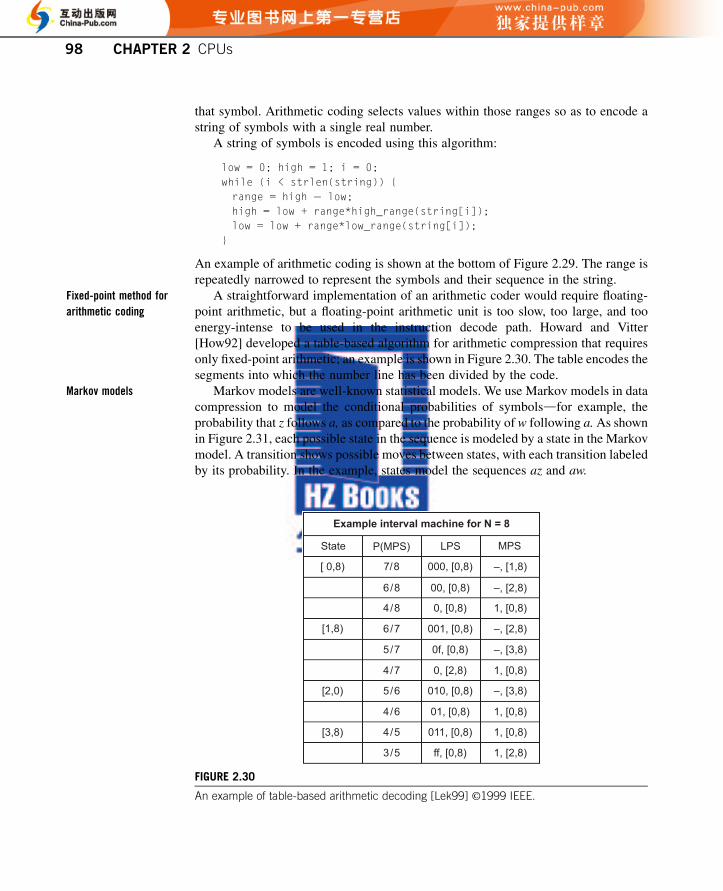
that symbol. Arithmetic coding selects values within those ranges so as to encode astring of symbols with a single real number.
A string of symbols is encoded using this algorithm:
low = 0; high = 1; i = 0;while (i < strlen(string)) {range = high e low;high = low + range*high_range(string[i]);low = low + range*low_range(string[i]);
}
An example of arithmetic coding is shown at the bottom of Figure 2.29. The range isrepeatedly narrowed to represent the symbols and their sequence in the string.
A straightforward implementation of an arithmetic coder would require floating-point arithmetic, but a floating-point arithmetic unit is too slow, too large, and tooenergy-intense to be used in the instruction decode path. Howard and Vitter[How92] developed a table-based algorithm for arithmetic compression that requiresonly fixed-point arithmetic; an example is shown in Figure 2.30. The table encodes thesegments into which the number line has been divided by the code.
Markov models are well-known statistical models. We use Markov models in datacompression to model the conditional probabilities of symbolsdfor example, theprobability that z follows a, as compared to the probability of w following a.As shownin Figure 2.31, each possible state in the sequence is modeled by a state in the Markovmodel. A transition shows possible moves between states, with each transition labeledby its probability. In the example, states model the sequences az and aw.
Example interval machine for N = 8
State P(MPS) LPS MPS
[ 0,8)
[1,8)
7/8
6/8
4/8
6/7
5/7
4/7
[2,0)
[3,8)
5/6
4/6
4/5
3/5
000, [0,8)
001, [0,8)
00, [0,8)
0, [0,8)
0f, [0,8)
0, [2,8)
010, [0,8)
01, [0,8)
011, [0,8)
ff, [0,8)
–, [1,8)
–, [2,8)
–, [2,8)
–, [3,8)
1, [0,8)
1, [0,8)
–, [3,8)
1, [0,8)
1, [0,8)
1, [2,8)
FIGURE 2.30
An example of table-based arithmetic decoding [Lek99] ©1999 IEEE.
Fixed-point method for
arithmetic coding
Markov models
98 CHAPTER 2 CPUs

The Markov model describes the relationship between the bits in an instruction.As shown in Figure 2.32, each state has two transitions, one for a 0 bit and one fora 1 bit. Any particular instruction defines a trajectory through the Markov model.Each state is marked with the probability of the most probable bit and whether thatbit is 0 or 1. The largest possible model for a block of b bits has 2b states, which istoo large. We can limit the size of the model in two ways: (1) limit the width by wrap-ping around transitions so that a state may have more than one incoming transition,and (2) limit the depth in a similar way by cutting off the bottom of the model andwrapping around transitions to terminate at existing states. The depth of the modelshould divide the instruction size evenly or be a multiple of the instruction size sothat the root state always falls on the start of an instruction.
a
az
aw
0.1
0.05
FIGURE 2.31
A Markov model for conditional character probabilities.
Subfieldop address
0110011101010110
Sample instruction
0.875
a
b c
0
0
00 0 0 0
0
1
1
1 11
1
1
12 3
4 5 6 7
8 9 10 11
0 2 20 1 3 31
Width
Model
Depth
FIGURE 2.32
A Markov model of an instruction.
2.7 Encoding and security 99

Lekatsas and Wolf compared SAMC to both ARM and Thumb. As shown inFigure 2.33, SAMC created smaller programs than Thumbdcompressed ARM pro-grams were smaller than Thumb, and compressed Thumb programs were also smaller.Lekatsas andWolf [Lek98, Lek99c] combined arithmetic coding andMarkovmodelsin the SAMC algorithm. Arithmetic coding provides more efficient codes than Huff-man coding but requires more careful coding. Markov models allow coding to takeadvantage of the relationships between strings of symbols.
Xie et al. [Xie02] used Tunstall coding [Tun67] to create fixed-sized code blocksfrom variable-sized segments of program text. Tunstall coding creates a coding treewith 2N leaf nodes and assigns an equal-length code to each leaf node. Because thedepth of the tree varies at different points, the input sequences that generate theleaf nodes, as described by paths from the root to leaves, can vary. This allows severalparallel decoders to independently decode different segments of the compressed datastream. Xie et al. added a Markov model to the basic Tunstall method to improve theresulting compression ratio. Variable-to-fixed encoding means that the decoder canfetch fixed-length blocks to decode into variable-length code segments. The parallelcoder cannot be used with Markov models since the current block must be decoded toknow which codebook to use for the next block. They also showed that the choice ofcodewords, which was arbitrary in Tunstall’s method, affects the energy consumptionof the decoder by reducing bit toggling on the compressed instruction bus. Figure 2.34shows the results of compressing code for a TI TMS320C6x processor using bothbasic Tunstall coding and a 32 � 4 Markov model. The compression ratio is not asgood as some other encoding methods but may be offset by the simplified decoder.
Several groups have proposed code compression schemes that use software rou-tines to decompress code. Liao et al. [Lia95] used dictionary-based methods. Theyidentified common code sequences and placed them into a dictionary. Instances ofthe compressed sequences were replaced by a call/return to a mini-subroutine thatexecuted the code. This method allowed code fragments to have branches as longas the block had a unique exit point. They also proposed a hardware implementation
0.8
0.6
0.4
0.2
0.0
DES Fft
Luca
s
Mpe
g2en
code
Mpe
g2de
code
Reed
Sol
omon
Xlisp
Thumb code size vs. ARM code size SAMC (ARM code) size vs. ARM code size SAMC (Thumb code) size vs. ARM code sizeSAMC (Thumb code) size vs. Thumb code size
Com
pres
sion
ratio
s
FIGURE 2.33
SAMC vs. ARM and Thumb [Lek99] ©1999 IEEE.
Arithmetic coding and
Markov models
Variable-to-fixed
encoding
Software-based
decompression
100 CHAPTER 2 CPUs

of this method that did not require an explicit return. They found instruction se-quences by dividing the code into basic blocks by comparing blocks against eachother and themselves at every possible region of overlap. They reported an averagecompression ratio of 70%.
0.95
0.9
0.85
0.8
0.75
0.7
adpc
mad
pcm
bloc
k_m
se
bloc
k_m
se
firfir
g721
g721
iiriir
mac
_vse
lpm
ac_v
selp
max
min
max
min
mod
emm
odem
mpe
gm
peg
n-bit Tunstall coding2-bit 3-bit 4-bit 6-bit5-bit
0.90.85
0.75
0.650.6
0.55
0.450.4
0.5
0.7
0.8
pegw
itpe
gwit
verti
bive
rtibi
2-bit-T 3-bit-T 4-bit-T32x4 Markov model and Tunstall coding
FIGURE 2.34
Code compression using variable-to-fixed coding for the TI TMS320C6x processor [Xie02]
©2002 IEEE.
2.7 Encoding and security 101

Kirovski et al. [Kir97] proposed a procedure cache for software-controlled codecompression. The procedure cache sits parallel to the instruction and data caches. Theprocedure cache is large enough to hold an entire decompressed procedure. Ratherthan directly embedding procedure addresses in subroutine call instructions, theyuse a table to map procedure identifiers in the code to the location of compressed pro-cedures in memory. In addition to decompressing procedures, their handler alsomanaged free space and reduced fragmentation in the procedure cache. This meansthat a calling procedure might be expunged from the procedure cache while it is wait-ing for a subroutine to return (consider, for example, a deep nest of procedure calls).The procedure call stores the identifier for the calling procedure, the address of thestart of the calling procedure at the time it was called, and the offset of the callfrom the start of the calling procedure.
Lefurgy et al. [Lef00] proposed adding a mechanism to allow software to writeinto the cache: an exception is raised on a cache miss; an instruction cache modifica-tion instruction allows the exception handler to write into the cache. They also pro-posed adding a second register file for the exception handler to reduce the overheadof saving and restoring registers. They use a simple dictionary-based compressionalgorithm. Every compressed instruction is represented by a 16-bit index. They alsoexperimented with the compression algorithm used by IBM CodePack. In addition,these authors developed an algorithm for selectively compressing programs bymeasuring the cache misses on sample executions and selecting the most frequentlymissing sections of code for compression.
Figure 2.35 shows the results of their experiments with instruction cache size.Lefurgy et al. tested both their dictionary compression algorithm and the CodePackalgorithm for several different cache sizes: 4KB, 16KB, and 64KB; they tested thesecache sizes both with a single register file and with the added register file for theexception handler. Figure 2.36 shows the performance of selectively compressed pro-grams relative to uncompressed code. The plots show relative performance as a func-tion of the percentage of the program that has been compressed for severalbenchmarks. In several cases (notably ijpeg, mpeg2enc, perl, and pegwit), the com-pressed program was somewhat faster, a fact that they attribute to changes in cachebehavior due to different procedure placement in the compressed versus uncom-pressed programs.
Chen et al. [Che02] proposed software-controlled code compression for Java. Thismethod compresses read-only data, which includes virtual machine binary code andJava class libraries. Read-only data is put in scratch pad memory on decompression.Compression allows some blocks in the on-chip memory system to be turned off andothers to be operated in low-power modes.
2.7.2 Code and data compressionGiven the success of code compression, it is reasonable to consider compressing bothcode and data and decompressing them during execution. However, maintaining com-pressed data in memory is more difficult. While instructions are (for the most part)
102 CHAPTER 2 CPUs

only read, data must be both read and written. This requires that we be able tocompress on the fly as well as decompress, leading to somewhat different trade-offsfor code/data compression than for code compression.
Lempel-Ziv coding [Ziv77] has been used for joint code/data compression. Itbuilds a dictionary for coding in a way that does not require sending the dictionaryalong with the compressed text. As shown in Figure 2.37, the transmitter uses a bufferto recognize repeated strings in the input text; the receiver keeps its own buffer to
6
5
4
3
2
1
00% 1% 2% 3% 4% 5% 6% 7% 8%
Exec
utio
n tim
e re
lativ
e to
nat
ive
code
Exec
utio
n tim
e re
lativ
e to
nat
ive
code
Instruction cache miss ratio
Instruction cache miss ratio
(a) Dictionary
D 4KB D 16KB D 64KBD+RF 16KB
40
35
30
25
20
15
10
5
00% 1% 2% 3% 5% 6% 7% 8%4%
(b) CodePackCP 4KB CP 16KB CP 64KBCP+RF 16KB
D+RF 4KBD+RF 64KB
CP+RF 64KBCP+RF 4KB
FIGURE 2.35
Execution time vs. instruction cache miss ratio [Lef00] ©2000 IEEE.
LempeleZiv coding
2.7 Encoding and security 103

record repeated strings as they are received so that they can be reused in later steps ofthe decoding process. The LempeleZiv coding process is illustrated in Figure 2.38.The compressor scans the text from first to last character. If the current string,including the current character, is in the buffer, then no text is sent. If the current string
201816141210
86420
50% 50%60% 60%70% 70%80% 80%90% 90%100% 100%
50% 60% 70% 80% 90% 100%
50% 60% 70% 80% 90% 100%
50% 60% 70% 80% 90% 100%
Compression ratioccI
Slow
dow
n
(a) (e)
(f)
(g)
(h)
(b)
(c)
(d)
43.5
2.5
1.5
0.50
1
2
3
50%
50%
50%
60%
60%
60%
70%
70%
70%
80%
80%
80%
90%
90%
90%
100%
100%
100%
ghostscript
121086450
go
1.61.51.41.31.21.1
10.9
ijpegCP exac CP miss D exac D miss
1.061.051.041.03
1.011.02
10.99
mpeg2enc
pegwit
perl
1.121.1
1.081.061.041.02
10.98
121086420
14121086420
vortex
FIGURE 2.36
Relative performance of selective compression [Lef00] ©2000 IEEE.
104 CHAPTER 2 CPUs

is not in the buffer, it is added to the buffer. The sender then transmits a token for thelongest recognized string (the current string minus the last character) followed by thenew character.
The LempeleZiveWelch (LZW) algorithm [Wel84] uses a fixed-size buffer forthe LempeleZiv algorithm. LZW coding was originally designed for disk drivecompression, in which the buffer is a small amount of RAM; it is also used for imageencoding using the GIF format.
Tremaine et al. [Tre01] developed the MXT memory system to make use of com-pressed data and code. A level 3 cache is shared among several processors; it talks tomain memory and to I/O devices. Data and code are uncompressed as they move frommain memory to the L3 cache and compressed when they move back to main memory.MXT uses a derivative of the 1977 LempeleZiv algorithm. A block to be compressedis divided into several equal-sized parts, each of which is compressed by an indepen-dent engine. All the compression engines share the same dictionaries. Typically,one-kilobyte blocks are divided into four 256-byte blocks for compression. Thedecompressor also uses four engines.
Benini et al. [Ben02] developed a data compression architecture with acompression/decompression unit between cache and main memory. They evaluatedseveral different compression algorithms and evaluated them for both compressionratio and energy savings. One algorithm they tested was a simple dictionary-basedcompression algorithm that stored the n most frequent words and their codes in adictionary. This algorithm gave an average of 35% less energy consumption.
Lekatsas et al. [Lek04] developed an architecture that combined compression andencryption of data and code. The encryption method must support random access ofdata so that large blocks do not need to be decrypted to allow access to a small piece ofdata. Their architecture modifies the operating system to place compression and
Sourcetext Coder Decoder
Dictionary Dictionary
Compressed text Uncompressed source
FIGURE 2.37
The Lempel-Ziv encoding/decoding process.
egegbaaa egegbaaa egegbaaa
Position Position Position
Table Table Table
a α aaa
αβ
aaaaaa
αβγ
FIGURE 2.38
An example of Lempel-Ziv encoding.
LempeleZiveWelch
coding
MXT memory system
Compression for energy
savings
Compression and
encryption
2.7 Encoding and security 105

encryption operations at the proper points in the memory access process; the systemdesigner can use a variety of different compression or encryption algorithms. A tablemaps uncompressed addresses to locations in compressed main memory.
2.7.3 Low-power bus encodingThe buses that connect the CPU to the caches and main memory account for a signif-icant fraction of all the energy consumed by the CPU. These buses are both wide andlong and have a large capacitance. They are also frequently used, with many switchingevents driving that large capacitance.
A number of bus encoding systems have been developed to reduce bus energyconsumption. As shown in Figure 2.39, information to be placed on the bus is firstencoded at the transmitting end and then decoded at the receiving end. The memoryand CPU do not know that the bus data is being encoded. Bus encoding schemes mustbe invertibledwe must be able to losslessly recover the data at the receiving end.Some schemes require side information, usually a small number of bits to helpdecode. Other schemes do not require side information to be transmitted alongsidethe bus.
The most important metric for a bus encoding scheme is energy savings. Becausethe energy itself depends on the physical and electrical design of the bus, we usuallymeasure energy savings using toggle counts. Because bus energy is proportional tothe number of transitions on each line in the bus, we can use toggle count as a relativeenergy measure. Toggle counts measure toggles between successive bits on a givenbus signal. Because crosstalk also reduces power consumption, some schemes alsolook at the values of physically adjacent bus signals. We are also interested in thetime, energy, and area overhead of the encoder and decoder. All these metrics mustinclude the toggle counts and other costs of any side information that is used forbus encoding.
Stan and Burleson proposed bus-invert coding [Sta95] to reduce the energy con-sumption of busses. This scheme takes advantage of the correlation between succes-sive values on the bus. Aword on the bus may be transmitted either in its original formor inverted form to reduce the number of transitions on the bus.
As shown in Figure 2.40, the transmitter side of the bus (for example, the CPU)stores the previous value of the bus in a register so that it can compare the currentbus value to the previous value. It then computes the number of bit-by-bit transitions
Cache/ memory Encoder
Side information
Decoder CPU
Bus
FIGURE 2.39
Microarchitecture of an encoded bus.
Bus encoding
Metrics
Bus-invert coding
106 CHAPTER 2 CPUs

using the function majority ðXORðBt;Bt�1ÞÞ, where Bt is the bus value at time t. Ifmore than half the bits of the bus change value from time t to time t � 1, then theinverted form of the bus value is transmitted; otherwise, the original form of thebus value is transmitted. One extra line of side information is used to tell the receiverwhether it needs to reinvert the value.
Stan and Burleson also proposed breaking the bus into fields and applying bus-invert coding to each field separately. This approach works well when data is naturallydivided into sections with correlated behavior.
Musoll et al. [Mus98] developed working-zone encoding for address buses(Figure 2.41). Their method is based on the observation that a large majority of theexecution time of programs is spent within small ranges of addresses, such as duringthe execution of loops. They divide program addresses into sets known as workingzones. When an address on the bus falls into a working zone, the offset from thebase of the working zone is sent in a one-hot code. Addresses that do not fall intoworking zones are sent in their entirety.
Benini et al. [Ben98] developed a method for address bus encoding. They clusteraddress bits that are correlated, create efficient codes for those clusters, then usecombinational logic to encode and decode those clustered signals.
They compute correlations of transition variables:
hðtÞi ¼
hxðtÞi $
�xðt�1Þi
�0i�h�
xðtÞi
�0$x
ðt�1Þi
i(EQ 2.25)
where hðtÞi is 1 if bit i makes a positive transition, �1 if it makes a negative transition,
and 0 if it does not change. They compute correlation coefficients of this function forthe entire address stream of the program.
In order to make sure that the encoding and decoding logic is not too large, wemust control the sizes of the clusters chosen. Benini et al. use a greedy algorithmto create clusters of signals with controlled maximum sizes. They use logic synthesistechniques to design efficient encoders and decoders for the clusters.
CPU
Majority
n1
nn Memory
FIGURE 2.40
The bus-invert coding architecture.
Working-zone encoding
Address bus encoding
2.7 Encoding and security 107

Table 2.1 shows the results of experiments by Benini et al., comparing theirmethod to working-zone encoding.
Lv et al. [Lv03] developed a bus encoding method that uses dictionaries. Thismethod is designed to consider both correlations between successive values and cor-relations between adjacent bits. They use a simple model of energy consumption for apair of lines: the function ENS(V t,V t-1) is 0 if both lines stay the same, 1 if one of the
for 1≤ i ≤ H + M do ∆1 = current Pref1if ∃∆r such that —n/2 ≤ ∆r ≤ n/2 — 1 thenoffset = ∆rPref _miss = 0ident = rif offset = prev_offr then
word = prev_sentelse word = transition—signaling[one-hot(offset)]Prefr = currentPrev_offr=offsetPref_ident = rif H + 1≤ r ≤ H + M then
prefj = current (1 ≤ j ≤ H)prev_offj = offset
elsePref_miss =1ident = prev_ identword = currentif M ≠ 0 then Prefj = current (H + 1≤ j ≤ H + M)else Prefj = current (1 ≤ j ≤ H)(leave prev_offj as before)
Prev_sent_word
(1) Active working zone search; in this work, fully associative(2) Replacement algorithum; in this work, LRU(3) ident is don’t care; its previous value is sent(4) prev_off is not modified since no previous offset is known
if pref_miss = 0 then xor = prev_received XOR word if xor = 0 then current = Prefident + prev_offident
(leave prev_offident as before)else current = Prefident + one-hot-retrieve(xor)
if ident > H thenPrefj = current, (1≤ j ≤ H)if xor = 0 then (leave prev_offj as before)else
prev_offj = one-hot-retrieve(xor)else
current = word Prefj = current(leave prev_offj as before)
prev_offident = one-hot-retrieve(xor)
(1)
(2) (2)
(3)
(2)
(2)(4)
(4)
Prefident = current
-
prev_received = word
FIGURE 2.41
Working-zone encoding and decoding algorithms [Mus98] ©1998 IEEE.
TABLE 2.1 Experimental evaluation of address encoding using the method of Benini et al. [Ben98]©1998
IEEE
Benchmark Length Binarytransitions
Benini et al.transitions
Beninisavings
Working-zonetransitions
Working-zonesavings
Dashboard 84,918 619,690 443,115 28.4% 452,605 26.9%
DCT 13,769 48,917 31,472 35.6% 36,258 25.8%
FFT 23,441 138,526 85,653 38.1% 99,814 27.9%
Matrix multiplication 22,156 105,947 60,654 42.7% 72,881 31.2%
Vector–vectormultiplication
19,417 133,272 46,838 64.8% 85,473 35.8%
Dictionary-based bus
encoding
108 CHAPTER 2 CPUs

two lines changes, and 2 if both lines change. They then model energy in terms oftransition (ET) and interwire (EI) effects:
ETðkÞ ¼ CLV2DD
X0�i�N�1
ENSðViðk � 1Þ;ViðkÞÞ (EQ 2.26)
EIðkÞ ¼ CLV2DDr
X0�i�N�2
ENI½Viðk � 1Þ;Viþ1ðkÞ;ViðkÞ;Viþ1ðkÞ� (EQ 2.27)
r ¼ inter � wire capacitance
CL(EQ 2.28)
EN(k) gives the total energy on the kth bus transaction.Dictionary encoding makes sense for buses because many values are repeated on
buses. Figure 2.42 shows the frequency of the ten most common patterns in a set ofbenchmarks. A very small number of patterns clearly accounts for a majority of thebus traffic in these programs. This means that a small dictionary can be used to encodemany of the values that appear on the bus.
Figure 2.43 shows the architecture of the dictionary-based encoding scheme. Boththe encoder and decoder have small dictionaries built from static RAM. Not all of theword is used to form the dictionary entry; only the upper bits of the word are used tomatch. The remaining bits of the word are sent unencoded. Lv et al. divide the bus intothree sections: the upper part of width Newiewo, the index part of width wi, and thebypassed part of width wo. If the upper part of the word to be sent is in the dictionary,the transmitter sends the index and the bypassed part. When the upper part is not used,those bits are put into a high-impedance state to save energy. Side information tells
100.00%
90.00%
80.00%
70.00%
60.00%
50.00%
40.00%
30.00%
20.00%
10.00%
0.00%bl
owfis
hdec
CRC3
2
FFT
gsmgo
ispel
l
jpeg
lam
e
qsor
trs
ynth
AVG
FIGURE 2.42
Frequency of the ten most frequent patterns in a set of benchmarks [Lv03] ©2003 IEEE.
2.7 Encoding and security 109

when a match is found. Some results are summarized in Figure 2.44; Lv et al. foundthat this dictionary-based encoding scheme saved about 25% of bus energy on datavalues. The hardware cost of this method was two additional bus lines for side infor-mation and about 4400 gates.
2.7.4 SecurityAs we saw in Section 1.5, security is composed of many different attributes: authen-tication, integrity, etc. Embedded processors require the same basic security featuresseen in desktop and server systems and they must guard against additional attacks.
Encoder
DictionaryUpper_part0Upper_part1
Upper_partn
DecoderBus
...
.
Status line
WR
wowi
Dictionary
Data[0:wo − 1]Data[wo:wo + wi − 1]
N−wi−wo]
Data[wo + wi:N − 1]
1
Upper_partn
Upper_part0Upper_part1
...
.
Tri
Data[wo + wi:N − 1]
1
Tri
=?
FIGURE 2.43
Architecture of the dictionary-based bus encoder of Lv et al. [Lv03] ©2003 IEEE.
4 5 6
34
56
3
0.3
0.2
0.1
0
4wi
wo
Ener
gy re
duct
ion
(1=
100%
)
FIGURE 2.44
Energy savings of dictionary-based code compression [Lv03] ©2003 IEEE.
110 CHAPTER 2 CPUs

Cryptographic operations are used in key-based cryptosystems. Cryptographic op-erations, such as key manipulation, are part of protocols that are used to authenticatedata, users, and transactions. Cryptographic arithmetic requires very long word oper-ations and a variety of bit- and field-oriented operations. A variety of instruction setextensions have been proposed to support cryptography. Co-processors may also beused to implement these operations.
Embedded processors must also guard against attacks. Attacks used againstdesktop and server systemsdTrojan horses, viruses, etc.dcan be used againstembedded systems. Because users and adversaries have physical access to theembedded processor, new types of attacks are also possible. Side channel attacksuse information leaked from the processor to determine what the processor is doing.
Smart cards are an excellent example of a widely used embedded system withstringent security requirements. Smart cards are used to carry highly sensitive datasuch as credit and banking information or personal medical data. Tens of millionsof smart cards are in use today. Because the cards are held by individuals, they arevulnerable to a variety of physical attacks, either by third parties or by the cardholder.
The dominant smart card architecture is called the self-programmable one-chipmicrocomputer (SPOM) architecture. The electrically programmable memoryallows the processor to change its own permanent program store.
SPOM architectures allow the processor to modify either data or code, includingthe code that is being executed. Such changes must be done carefully to be sure thatthe memory is changed correctly and CPU execution is not compromised. Ugon[Ugo83] proposed a self-reprogrammable architecture. The memory is divided intotwo sections: both may be EPROM or one may be ROM, in which case the ROM sec-tion of the memory cannot be changed. The address and data are divided among thetwo programs. Registers are used to hold the addresses during the memory operationas well as to hold the data to be read or written. One address register holds the addressto be read/written while the other holds the address of a program segment that controlsthe memory operation. Control signals from the CPU determine the timing of thememory operation. Segmenting the memory access into two parts allows arbitrary lo-cations to be modified without interfering with the execution of the code that governsthe memory modification. Because of the registers and control logic, even the loca-tions that control the memory operation can be overwritten without causing opera-tional problems.
The next example describes security features on ARM processors.
Example 2.5 ARM SecurCore�
SecurCore [ARM05B] is a series of processors designed for smart cards and related applica-tions. They support cryptographic operations using the SafeNet cryptographic co-processor.The SafeNet EIP-25 co-processor [ARM05C] can perform 1024-bit modular exponentiationand supports keys up to 2048 bits. The SecurCore processors provide memory managementunits that allow the operating system to manage access capabilities.
Cryptography and CPUs
Varieties of attacks
Smart cards
Self-reprogramming
architecture
2.7 Encoding and security 111

The SAFE-OPS architecture [Zam05] is designed to validate the state ofembedded software and protect against software modifications. The compiler embedsa watermarkda verifiable identifierdinto the code using register assignment. Ifeach register is assigned a symbol, then the sequence of registers used in a sectionof code represents the watermark for that code. A field-programmable gate array(FPGA) attached to the system bus can monitor the instruction stream and extractthe watermark during execution. If the watermark is invalid, then the FPGA can signalan exception or otherwise take action.
Side channel attacks, as mentioned above, use information emitted from theprocessor to determine the processor’s internal state. Electronic systems typi-cally emit electromagnetic energy that can be used to infer some of the circuit’sactivity. Similarly, the dynamic behavior of the power supply current can beused to infer internal CPU state. Kocher et al. [Koc99] showed that, using atechnique they call differential power analysis, measurements of the power sup-ply current into a smart card could be used to identify the cryptosystem key stored inthe smart card.
Countermeasures have been developed for power attacks. Yang et al. [Yan05] useddynamic voltage and frequency scaling to mask operations in processors as shown inFigure 2.45. They showed that proper design of a DVFS schedule can make it substan-tially harder for attackers to determine internal states from processor power consump-tion. Figure 2.46 shows traces without (a and c) and with (b and d) DVFS-basedprotection.
Several methods have been developed to generate a unique signature for eachmanufactured integrated circuit using manufacturing process variations. The ICmanufacturing process exhibits natural variations that cause variations in the param-eters of devices and wires on the chips. Many device variations can be observed be-tween chips, even on the same wafer. Those variations can be used as a signature forthe chip; if a given chip is swapped with a different chip, the tampering can bedetected through the change in device signatures. Lofstrom et al. [Lof00] used anarray of transistors and addressing circuitry that allowed a checker to selectively con-nect to the drain of one of those transistors. The checker uses the transistor’s drain
CPU
Clock
DVFS controllerDVFS scheduler
Voltage
FIGURE 2.45
A DVFS-based measure to protect against power attacks.
SAFE-OPS
Power attacks
Countermeasures
Device fingerprints and
PUFs
112 CHAPTER 2 CPUs

current to drive a load resistor; the sequence of voltages derived by testing each of thetransistors in the array serves as the chip’s signature. They showed that an array of 112identification cells could reliably distinguish over 1 million signatures with a less than10�1 10�0 error rate. Lim et al. [Lim05] used arbiters to build physically unclonablefunctions (PUFs) to create device signatures. They use an arbiter to compare thedelay of two copies of the same function. This structure minimizes the sensitivityof the delay measurement to temperature and other environmental factors that affectdelay.
2.8 CPU simulationCPU simulators are essential to computer system design. CPU architects use simula-tors to evaluate processor designs before they are built. System designers use simula-tors for a variety of purposes: analyzing the performance and energy consumption of
(a) DES Encryption DES Encryption
DES Encryption
Time (nanosecond) Time (nanosecond)
Time (nanosecond)Time (nanosecond)
DES Encryption
(b)
(c) (d)
0.05 0.04 0.03
0.02
0.01
0
0.01
0.02
0.03
0.04
0.05
0.05 0.04 0.03
0.02
0.01
0
0.01
0.02
0.03
0.04
0.05
0.05 0.04 0.03
0.02
0.01
0
0.01
0.02
0.03
0.04
0.05
0.05 0.04 0.03
0.02
0.01
0
0.01 0.02 0.03 0.04 0.05
0 1 2 3 4 5
0 1 2 3 4 50 0.5 1 1.5 2 2.5 3 3.5 4 4.5
0 0.5 1 1.5 2 2.5 3 3.5 4 4.5×103 ×103
×103×105
Pow
er d
iffer
ence
(Wat
t)P
ower
diff
eren
ce (W
att)
Pow
er d
iffer
ence
(Wat
t)P
ower
diff
eren
ce (W
att)
FIGURE 2.46
Traces without and with DVFS protection [Yan05] ©2005 ACM.
2.8 CPU simulation 113

programs; simulating multiprocessors before and after they are built; and systemdebugging.
The term “CPU simulator” is generally used broadly to mean any method ofanalyzing the behavior of programs on processors. We can classify CPU simulationmethods along several lines:
• Performance vs. energy/power/thermaldSimulating the energy or power con-sumption of a processor requires accurate simulation of its internal behavior. Sometypes of performance-oriented simulation, in contrast, can perform a less detailedsimulation and still provide reasonably accurate results. Thermal modeling isrelated to power modeling.
• Temporal accuracydBy simulating more details of the processor, we can obtainmore accurate timings. More accurate simulators take more time to execute.
• Trace vs. executiondSome simulators analyze a trace taken from a program thatexecutes on the processor, while others analyze the program execution directly.
• Simulation vs. direct executiondSome execution-based systems directlyexecute on the processor being analyzed while others use simulation programs.
Simulation is generally driven by programs and data. To obtain useful results fromsimulation, we need to simulate the right programs that are working on reasonableinput data. The application code itself is the best way to exercise an embedded system,but benchmark suites can help us evaluate architectures when we do not yet havethe code.
Engblom [Eng95] compared the SpecInt95 benchmarks with the properties ofseveral proprietary embedded programs (totaling 334,600 lines of C code) andconcluded that embedded software has very different characteristics than the SpecIntbenchmark set. The analysis was based upon static analysis of the program, using anintermediate representation of the programs to minimize differences introduced bycoding methods. Some of his results are summarized in Figure 2.47. He found thatdynamic data structures were more common in SpecInt95 and arrays and structswere more common in embedded programs. SpecInt95 used more 32-bit variables,while embedded programs used mostly smaller data; embedded programs also usedmany more unsigned variables. Embedded programs used more static and global vari-ables, and also used more logic operations than did SpecInt95. He also found thatembedded programs had more trial functions that made no decisions and fewer com-plex functions with loops.
The next two examples introduce two sets of benchmarks for embeddedcomputing applications.
Example 2.6 MediaBench IIMediaBench II [SLU13, Lee97] is a benchmark set designed to represent workloads for multi-media and communication applications. It includes several components, such as H.264,JPEG-2000, MPEG-2, H.263, and JPEG. The suite includes sample data as well as code.
114 CHAPTER 2 CPUs

Example 2.7 EEMBC DENBenchThe Embedded Microprocessor Benchmark Consortium (EEMBC) (http://www.eembc.org) de-velops and maintains benchmarks for a variety of embedded system application areas. TheDENBench suite [Lev05] is designed to characterize digital entertainment systems, both mo-bile and installed. DENBench is composed of four minisuites: MPEG EncodeMark, MPEGDecodeMark, CryptoMark, and ImageMark. The final score is the geometric mean of the fourminisuites.
This section surveys techniques for CPU simulation: first we cover trace-basedanalysis, then direct execution, then simulators that model the CPUmicroarchitecture.
Embedded
Distribution of lengths of integer typesDistribution of variables across types
Distribution of variables across scopes
Distribution of function complexity
Distribution of operator categories
Speclnt95
1.0%2.1%14.0%70.8%
2.7% 9.4%
longshortcharunsignedsigned
0%10%20%30%40%50%60%70%80%90%
100%
0%10%20%30%40%50%60%70%80%90%
100%
53.1%44.9%0.4%1.3%
0.0% 0.3%
longshortcharunsignedsigned
Code Pointer
Pointer
Array
Integer
Struct/Union
0.0%Float 0.5%
3.5%9.9%
10%0% 20% 30% 40% 50% 60%
0% 10% 15% 25% 35% 45%5% 20% 30% 40% 50% 0% 10% 20% 30% 40% 50% 60%
Trivial
Embedded Speclnt95
Non-looping Complex
60%
50%55%
45%40%35%30%
32.7%
16.2%
47.9% 48.1%
19.4%
36.7%
25%20%15%10%5%0%
43.55%
52.80%
25.77%
23.11%
29.0%
25.74%
11.39%
4.94%
12.70%
38.7%
0.8%
4.8%
7.5%
44.6%
47.1%
Global
Static
Auto
Parameters
Compares
Logic
Arithmetic
Pointer27.5%
3.1%
38.0%
11.8%
54.7%
22.0%
0.3%0.2%
56.1%
FIGURE 2.47
SpecInt 95 vs. embedded code characteristics [Eng99] ©1999 IEEE.
2.8 CPU simulation 115

2.8.1 Trace-based analysisTrace-based analysis systems do not directly operate on a program. Instead, they use arecord of the program’s execution, called a trace, to determine the characteristics ofthe processor.
As shown in Figure 2.48, trace-based analysis gathers information from a runningprogram. The trace is then analyzed after execution of the program being analyzed.The post-execution analysis is limited by the data gathered in the trace during pro-gram execution.
The trace can be generated in several different ways. The program can be instru-mented with additional code that writes trace information to memory or a file. Theinstrumentation is generally added during compilation or by editing the objectcode. The trace data can also be taken by a process that interrupts the program andsamples its program counter (PC); this technique is known as PC sampling. Thesetwo techniques are not mutually exclusive.
Execution
Instrumentedprogram
Trace
Analysis tool
Analysisresults
PC sampling
Code modificationtool
Program
Instrumentation-based
Sampling-based
FIGURE 2.48
The trace-based analysis process.
Tracing and analysis
116 CHAPTER 2 CPUs
Profiling information can be taken on a variety of types of program informationand at varying levels of granularity:
• Control flowdControl flow is useful in itself and a great deal of other informationcan be derived from control flow. The program’s branching behavior can generallybe captured by recording branches; behavior within the branches can be inferred.Some systems may record function calls but not branches within a function.
• Memory accessesdMemory accesses tell us about cache behavior. The behaviorof the instruction cache can be inferred from control flow. Data memory accessesare usually recorded by instrumentation code that surrounds each memory access.
An early and well-known trace-based analysis tool is the Unix prof command andits GNU cousin gprof [Fen98]. gprof uses a combination of instrumentation and PCsampling to generate the trace. The trace data can generate call-graph (procedure-level), basic-block-level, and line-by-line data.
Averydifferent typeof trace-basedanalysis tool is thewell-knownDinero tool [Edl03].Dinero is a cache simulator. It does not analyze the timing of a program’s execution,rather it only looks at the history of references to memory. The reference memory historyis captured by instrumentation within the program. After execution, the user analyzes theprogram behavior in the memory hierarchy using the Dinero tools. The user designs acache hierarchy in the form of a tree and sets the parameters for the caches for analysis.
Traces can be sampled rather than recorded in full [Lah88]. A useful executionmay require a great deal of data. Consider, for example, a video encoder that must pro-cess several frames to exhibit a reasonable range of behavior. The trace may besampled by taking data for a certain number of instructions and then not recording in-formation for another sequence of instructions. It is often necessary to warm up thecache before taking samples. The usual challenges of sampled data apply: an adequatelength of sample must be taken at each point and samples must be taken frequentlyenough to catch important behavior.
2.8.2 Direct executionDirect execution-style simulation makes use of the host CPU used for simulation inorder to help compute the state of the target machine. Direct execution is used primar-ily for functional and cache simulation, not for detailed timing.
The various registers of the computer comprise its state; we need to simulate thoseregisters in the target machine that are not defined in the host machine but we can usethe host machine’s native state where appropriate. A compiler generates code for thesimulation by adding instructions to compute the target state that needs to be simu-lated. Because much of the simulation runs as native code on the host machine, directexecution can be very fast.
2.8.3 Microarchitecture-modeling simulatorsWe can provide more detailed performance and power measurements by building asimulator that models the internal microarchitecture of the computer. Directly
prof
Dinero
Trace sampling
Emulating architectures
Modeling detail and
accuracy
2.8 CPU simulation 117

simulating the logic would provide even more accurate results but would be much tooslow, preventing us from running the long traces that we need to judge system perfor-mance. Logic simulation also requires us to have the logic design, which is not gener-ally available from the CPU supplier. But in many cases we can build a functionalmodel of the microarchitecture from publicly available information.
Microarchitecture models may vary in the level of detail they capture about themicroarchitecture. Instruction schedulers model basic resource availability butmay not be cycle-accurate. Cycle timers, in contrast, model the architecture inmore detail in order to provide cycle-by-cycle information about execution. Accuracygenerally comes at the cost of somewhat slower simulation.
A typical model for a three-stage pipelined machine is shown in Figure 2.49. Thismodel is not a register-transfer model in that it does not include the register file orbuses as first-class elements. Those elements are instead subsumed into the modelsof the pipeline stages. The model captures the main units and paths that contributeto data and control flow within the microarchitecture.
The simulation program consists of modules that correspond to the units in themicroarchitectural model. Because we want the simulator to run fast, these simulatorsare typically written in a sequential language such as C, not in a simulation languagelike Verilog or VHDL. Simulation languages have mechanisms to ensure that modulesare evaluated in the proper order when the simulation state changes; when we writesimulators in sequential languages, we must design the control flow in the programto ensure that all the implications of a given state change are properly evaluated.
DecodeFetch Execute
DMMUD$I$
Mainmemory
IMMU
FIGURE 2.49
A microarchitectural model for simulation.
Modeling for simulation
Simulator design
118 CHAPTER 2 CPUs

SimpleScalar [Sim05] is a well-known toolkit for simulator design. SimpleScalarprovides modules that model typical components of CPUs as well as tools for datacollection. These tools can be put together in various ways, modified, or added toin order to create a custom simulator. A machine description file describes the micro-architecture and is used to generate parts of the simulation engine as well as program-ming tools like disassemblers.
2.8.4 Power and thermal simulation and modelingPower simulators take cycle-accurate microarchitecture simulators one step furtherin detail. Determining the energy/power consumption of a CPU generally requireseven more accurate modeling than performance simulation. For example, a cycle-accurate timing simulator may not directly model the bus. But the bus is a major con-sumer of energy in a microprocessor, so a power simulator needs to model the bus, aswell as register files and other major structural components. In general, a power simu-lator most model all significant sources of capacitance in the processor since dynamicpower consumption is directly related to capacitance. However, power simulatorsmust trade-off accuracy for simulation performance just like other cycle-accurate sim-ulators. The two best-known power simulators are Wattch [Bro00] and SimplePower[Ye00]. Both are built on top of SimpleScalar and add capacitance models for themajor units in the microarchitecture.
Thermal modeling is related to powerdthe heat generated by a processor is deter-mined by its power consumption. However, materials exhibit thermal resistance andcapacitance with properties similar to electrical R and C. As a result, the temperatureof a chip can vary in space, depending on the relative power consumption of differentparts of the chip, and in time, as power consumption varies with activity and leakage.The relationship between power consumption and chip temperature can be modeledusing a differential equation [Ska04]:
CdT
dtþ T � Tamb
R¼ P (EQ 2.29)
where Tamb is the ambient temperature. The HotSpot 4.0 model [Hua08] is widelyused for thermal modeling. The model is implemented as a module to be integratedinto CPU simulators. The HotSpot block model analyzes heat flows using a modelderived from the block structure of the chip floorplan; it subdivides blocks withhigh aspect ratios to take into account the directional dominance of heat flow.It also models the package heat transfer characteristics.
2.9 Automated CPU designSystem designers have long used custom processors to run applications at higherspeeds. Custom processors were popular in the 1970s and 1980s thanks to bit-sliceCPU components. Chips for data paths and controllers, such as the AMD 2910 series,
SimpleScalar
Power simulation
Thermal modeling
2.9 Automated CPU design 119

could be combined and microprogrammed to implement a wide range of instructionsets. Today, custom integrated circuits and FPGAs offer complete freedom todesigners who are willing to put the effort into creating a CPU architecture for theirapplication. Custom CPUs are often known as application-specific instruction pro-cessors (ASIPs) or configurable processors.
Custom CPU design is an area that cries out for methodological and tool support.System designers need help determining what sorts of modifications to the CPU arefruitful. They also need help implementing those modifications. Today, system de-signers have a wide range of tools available to help them design their own processors.
We can customize processors in many different ways:
• Instruction sets can be adapted to the application.• New instructions can provide compound sets of existing operations, such as
multiply-accumulate.• Instructions can supply new operations, such as primitives for Viterbi encoding
or block motion estimation.• Instructions that operate on nonstandard operand sizes can be added to avoid
masking and reduce energy consumption.• Instructions not important to the application can be removed.
• Pipelines can be specialized to take into account the characteristics of function unitsused in new instructions, implement specialized branch prediction schemes, etc.
• The memory hierarchy can be modified by adding and removing cache levels,choosing a cache configuration, or choosing the banking scheme in a partitionedmemory system.
• Buses and peripherals can be selected and optimized to meet bandwidth and I/Orequirements.
ASIPs require customized versions of the tool chains that software developershave come to rely upon. Compilers, assemblers, linkers, debuggers, simulators, andIDEs (integrated development environments) must all be modified to match theCPU characteristics.
Tools to support customized CPU design come in two major varieties. Configura-tion tools take the microarchitecturedinstruction set, pipeline, memory hierarchy,etc.das a specification and create the logic design of the CPU (usually as register-transfer Verilog or VHDL) along with the compiler and other tools for the CPU.Architecture optimization tools help the designer select a particular instructionset and microarchitecture based upon application characteristics.
The MIMOLA system [Mar84] is an early example of both architecture optimi-zation and configuration. MIMOLA analyzed application programs to determineopportunities for new instructions. It then generated the structure of the CPU hard-ware and generated code for the application program for which the CPU wasdesigned.
We will defer our discussion of compilers for custom CPUs until the next chapter.In this section we will concentrate on architecture optimization and configuration.
Why automate CPU
design
Axes of customization
Software tools
Tool support
Early work
In this section
120 CHAPTER 2 CPUs

2.9.1 Configurable processorsCPU configuration spans a wide range of approaches. Relatively simple generatortools can create simple adjustments to CPUs. Complex synthesis systems can imple-ment a large design space of microarchitectures from relatively simple specifications.
Figure 2.50 shows a typical design flow for CPU configuration. The systemdesigner may specify instruction set extensions as well as other system parameterslike cache configuration. The system may also accept designs for function unitsthat will be plugged into the processor. Although it is possible to synthesize the micro-architecture from scratch, the CPU’s internal structure is often built around a proces-sor model that defines some basic characteristics of the generated processor. Theconfiguration process includes several steps, including allocation of the datapathand control, memory system design, and I/O and bus design. Configuration results
Instruction set specification
Parameters and components
CPU Configuration Data path
allocation
Controller synthesis
Memory system configuration
Interrupt systemgeneration
Bus generation
CPU RTL
RTL Synthesis
CPU core
Programming tools
Processor model
FIGURE 2.50
The CPU configuration process.
2.9 Automated CPU design 121

in both the CPU logic design and software tools (compiler, assembler, etc.) for theprocessor. Configurable processors are generally created in register-transfer formand used as soft IP. Standard register-transfer synthesis tools can be used to createa set of masks or an FPGA configuration for the processor.
Several processor configuration systems have been created over the years by bothacademic and industrial teams. The Synopsys Design Ware ARC family of configu-rable cores (https://www.synopsys.com/IP/PROCESSORIP/ARCPROCESSORS/) in-cludes several members: the HS family is a multicore processor; the 700 family has aseven-stage pipeline; the 600 family has a five-stage pipeline and DSP capabilities.
The next example describes a commercial processor configuration system.
Example 2.8 The Tensilica Xtensa Configurable ProcessorThe Tensilica Xtensa� configurable processor is designed to allow a wide range of CPUs to bedesigned from a very simple specification. An Xtensa core can be customized in many ways:
• The instruction set can be augmented with basic ALU-style operations, wide instructions,DSP-style instructions, or co-processors.
• The configuration of the caches can be controlled, memory protection and translation canbe configured, DMA access can be added, and addresses can be mapped into special-purpose memory.
• The CPU bus width, protocol, system registers, and scan chain can be optimized.• Interrupts, exceptions, remote debugging features, and standard I/O devices such as timers
can be added.
The following figure from Rowen [Row05] illustrates the range of features in the CPU thatcan be customized:
Trace
JTAG
Interrupts
Processor controls
ExtendedInstruction
align,decodeInstruction
MMU
Instruction ROM
Instruction RAM
Instructioncache
Instruction fetch/PCTRACE port
JTAG tap control
On-chip debug
Exception handlingregisters
Exception support
Userdefined registerfiles
Userdefined registerfiles
Userdefined executionunits User defined
execution unit
Floating pointWritebuffer
Base registerfile
Instruction addresswatch registers
Data addresswatch registers
Interrupt control
Timers
Base ISA feature Configurable function Optional function Optional and configurable
Userdefined executionunits andinterfaces
VLIW DSP VLIW DSPVLIW DSP
Used defined data load/store units
Dataload/storeunit
DataMMU
Data ROMsData RAMs
Datacache
Pifprocessorbusinterface
Xtensalocalmemoryinterface
Base ALU
MAC 16 DSP
MUL 16/32
External interface
Xtensaprocessorinterfacecontrol
Instructiondecode/dispatch
User defined features
122 CHAPTER 2 CPUs

Instructions are specified using the TIE language. TIE allows the designer to declarean instruction using state declarations, instruction encodings and formats, and operationdescriptions. For example, consider this simple TIE instruction specification (afterRowen):
Regfile LR 16 128 lOperation add128
{ out LR sr, in LR ss, in LR st } {}{ assign sr = st + ss; }
The Regfile declaration defines a large register file named LR with 16 entries, each 128bits wide. The add128 instruction description starts with a declaration of the arguments to theinstruction; each of the arguments is declared to be in the LR register file. It then defines theinstruction’s operation, which adds two elements of the LR register file and assigns it to a thirdregister in LR.
New instructions may be used in programs with intrinsic calls that map onto instructions.For example, the code out[i] = add128(a[i], b[i]) makes use of the new instruction.Optimizing compilers may also map onto the new instructions.
EEMBC compared several processors on benchmarks for consumer electronics, digitalsignal processing, and networking. These results [Row05] show that custom, configurableprocessors can provide much higher performance than standard processors:
0.5
0.5
0.4
0.4
0.3
0.2
0.2
0.3
2.02.0
1.5
1.0
0.5
0.0
0.10.0160.030.087 0.058 0.013 0.011
0.0 0.00
Optimized telemarks/MHzOptimized consumer marks/MHzExtensible optimized Extensible out-of-box MIPS64 20Kc
0.02
0.04
0.06
0.08
0.10
0.12
0.14
0.1
0.1230.473
0.018
0.03
0.017 0.016
0.010.080 0.059 0.039
DS
P
Net
wor
king
Con
sum
er E
lect
roni
cs
Optimized netmarks/MHz
MIPS32b (NEC VR4122)MIPS64b (NEC VR5000)ARM1020E
0.017
In order to evaluate the utility of configuration, Tensilica created customized processors forfour different benchmark programs:
• DotProd: Dot product of two 2048-element vectors• AES: Advanced Encryption Standard• Viterbi: Viterbi trellis decoder• FFT: 256-point fast Fourier transform
A different CPU was designed for each benchmark. The CPUs were implemented,measured, and compared to a baseline Xtensa processor without extensions. The performance,
2.9 Automated CPU design 123

power, and energy consumption of the processors show [Row05] that configuring customizedprocessors can provide large energy savings:
The design of a processor for a 256-point FFT computation illustrates how different typesof customizations contribute to processor efficiency. Here is the architecture for the proces-sor [Row05]:
DSP Data registers (66% active)
Processor-DSP overhead
Instruction fetch/decode
Instruction memory
Addressregisters
BaseALUpipeline
Data memory(83% active)
128bDSPload-storepipeline(83% active)
8 × 20bDSPALUpipeline(67% active)
4 × 16bDSPmultiplypipeline(100% active)
Configuration Metric DotProd AES Viterbi FFT
Reference processor Area (mm2) 0.9 0.4 0.5 0.4
Cycles (K) 12 283 280 326
Power (mW/MHz) 0.3 0.2 0.2 0.2
Energy (mJ) 3.3 61.1 65.7 56.6
Optimized processor Area (mm2) 1.3 0.8 0.6 0.6
Cycles (K) 5.9 2.8 7.6 13.8
Power(mW/MHz)
0.3 0.3 0.3 0.2
Energy (mJ) 1.6 0.7 2.0 2.5
Energyimprovement
2 82 33 22
Source: From Tensilica [Ten04] © 2004 Tensilica, Inc.
124 CHAPTER 2 CPUs

When we analyze the energy consumption of the subsystems in the processor, we find[Row05] that fine-grained clock gating contributed substantially to energy efficiency, followedby a reduction in processor-DSP overhead:
RTL Data pathwithoutfine-grainedclockgate
Processor withoutfine-grainedclock gate
Processor withfine-grainedclock gate
Engine implementation
W/M
Hz
pow
er (1
30 n
m 1
.0V)
Task engine power efficiency256 pt complex FFT (1078 cycles)
Instruction memoryData memory DSP data path
Base processor logic Processor-DSP overhead
700
600
500
400
300
200
100
0
The next example describes a configurable processor designed for media process-ing applications.
2.9 Automated CPU design 125
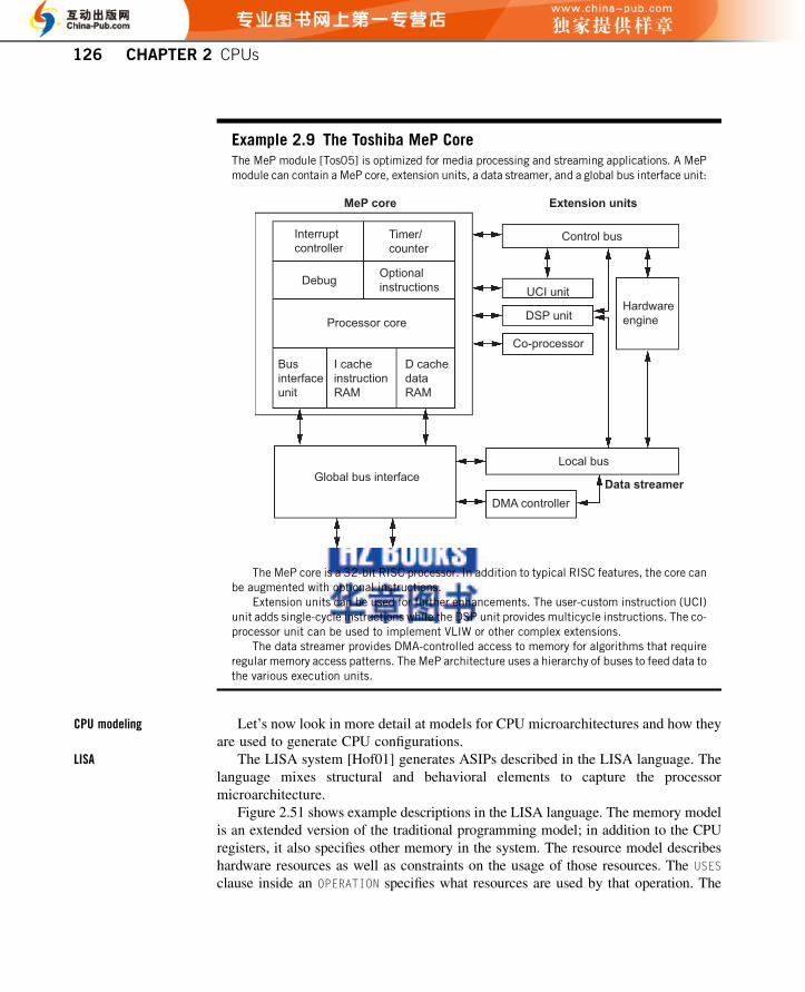
Example 2.9 The Toshiba MeP CoreThe MeP module [Tos05] is optimized for media processing and streaming applications. A MePmodule can contain a MeP core, extension units, a data streamer, and a global bus interface unit:
I cacheinstructionRAM
Businterfaceunit
Global bus interface
Processor core
Co-processor
Debug
DSP unit
UCI unit
Control bus
Hardwareengine
Optionalinstructions
Timer/counter
Interruptcontroller
D cachedataRAM
DMA controllerData streamer
Extension unitsMeP core
Local bus
The MeP core is a 32-bit RISC processor. In addition to typical RISC features, the core canbe augmented with optional instructions.
Extension units can be used for further enhancements. The user-custom instruction (UCI)unit adds single-cycle instructions while the DSP unit provides multicycle instructions. The co-processor unit can be used to implement VLIW or other complex extensions.
The data streamer provides DMA-controlled access to memory for algorithms that requireregular memory access patterns. The MeP architecture uses a hierarchy of buses to feed data tothe various execution units.
Let’s now look in more detail at models for CPU microarchitectures and how theyare used to generate CPU configurations.
The LISA system [Hof01] generates ASIPs described in the LISA language. Thelanguage mixes structural and behavioral elements to capture the processormicroarchitecture.
Figure 2.51 shows example descriptions in the LISA language. The memory modelis an extended version of the traditional programming model; in addition to the CPUregisters, it also specifies other memory in the system. The resource model describeshardware resources as well as constraints on the usage of those resources. The USESclause inside an OPERATION specifies what resources are used by that operation. The
CPU modeling
LISA
126 CHAPTER 2 CPUs
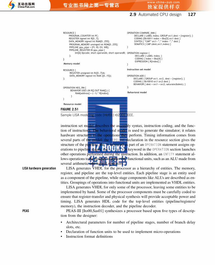
instruction set model describes the assembly syntax, instruction coding, and the func-tion of instructions. The behavioral model is used to generate the simulator; it relateshardware structures to the operations they perform. Timing information comes fromseveral parts of the model: the PIPELINE declaration in the resource section gives thestructure of the pipeline; the IN keyword as part of an OPERATION statement assigns op-erations to pipeline stages; the ACTIVATION keyword in the OPERATION section launchesother operations performed during the instruction. In addition, an ENTITY statement al-lows operations to be grouped together into functional units, such as an ALUmade fromseveral arithmetic and logical operators.
LISA generates VHDL for the processor as a hierarchy of entities. The memory,register, and pipeline are the top-level entities. Each pipeline stage is an entity usedas a component of the pipeline, while stage components like ALUs are described as en-tities. Groupings of operations into functional units are implemented as VHDL entities.
LISA generates VHDL for only some of the processor, leaving some entities to beimplemented by hand. Some of the processor components must be carefully coded toensure that register-transfer and physical synthesis will provide acceptable power andtiming. LISA generates HDL code for the top-level entities (pipeline/registers/memory), the instruction decoder, and the pipeline decoder.
PEAS-III [Ito00,Sas01] synthesizes a processor based upon five types of descrip-tion from the designer:
• Architectural parameters for number of pipeline stages, number of branch delayslots, etc.
• Declaration of function units to be used to implement micro-operations• Instruction format definitions
RESOURCE { PROGRAM_COUNTER int PC; REGISTER signed int R[0..7]; DATA_MEMORY signed int RAM[0..255];
RESOURCE { REGISTER unsigned int R([0..7])6; DATA_MEMORY signed int RAM ([0..15]);};
Memory model
Resource model
OPERATION COMPARE_IMM { DECLARE { LABEL index; GROUP src1,dest = {register}; } CODING {0b10011 index = 0bx[5] src1 dest } SYNTEX { “CMP” src1—”,” index—”,” dest } SEMATICS { CMP (dest,src1,index) }}
Instruction set model
OPERATION ADD { DECLARE { GROUP src1, src2, dest = {register}; } CODING { 0b10010 src1 src2 dest } BEHAVIOR { dest = src1 + src2; saturate(&dest); }};
Behavioral model
OPERATION register { DECLARE { LABEL index; } CODING { index = 0bx[4] } EXPRESSION { R[index] }}
OPERATION NEG_RM { BEHAVIOR USES (IN R[] OUT RAM[];) { RAM[address] = (—1) * R[index]; }}
PROGRAM_MEMORY unsinged int ROM[0..255];PIPELINE ppu_pipe = {FI; ID; EX; WB};PIPELINE_REGISTER IN ppu_pipe { bit[6] 0pcode; short operandA; short operandB;};
}
FIGURE 2.51
Sample LISA modeling code [Hof01] ©2001 IEEE.
LISA hardware generation
PEAS
2.9 Automated CPU design 127

• Definitions of interrupt conditions and timing• Descriptions of instructions and interrupts in terms of micro-operations
Figure 2.52 shows the model used by PEAS-III for a single pipeline stage. Thedatapath portion of a stage can include one or more function units that implement op-erations; a function unit may take one or more clock cycles to complete. Each stagehas its own controller that determines how the function units are used and when datamoves forward. The datapath and controller both have registers that present their re-sults to the next stage.
A pipeline stage controller may be in either the valid or invalid state. A stage maybecome invalid because of interrupts or other disruptions to the input of the instructionflow. A stage may also become invalid due to a multicycle operation, a branch, orother disruptions during the middle of instruction operation.
A pipeline model for the entire processor is built by concatenating several pipelinestages. The stages may also connect to other resources on both the datapath orcontroller side. Datapath stages may be connected to memory or caches. Controllerstages may be connected to an interrupt controller that coordinates activity duringexceptions.
PEAS-III generates two VHDL models, one for simulation and another for synthe-sis. The datapath is generated in three phases. First, the structures required for eachinstruction are generated independently: the function unit resources, the ports onthe resources, and the connections between those resources. The resource sets forthe instructions are then merged. Finally, multiplexers and pipeline registers are addedto control access to resources. After the datapath stages are synthesized, the control-lers can be generated. The controllers are synthesized in three stages: the control sig-nals required for the datapath multiplexers and registers are generated; the interlocksfor multicycle operations are then generated; and finally the branch control logic issynthesized. The interrupt controller is synthesized based upon the specificationsfor the allowed interrupts.
ASIP Meister [Kob03] is the follow-on system to PEAS. It generates Harvard ar-chitecture machines based upon estimations of area, delay, and power consumptionduring architecture design and micro-operation specification.
FU FU
Data path
Ctrl
Control
FIGURE 2.52
PEAS-III model of a pipeline stage.
PEAS pipeline structure
PEAS hardware synthesis
ASIP Meister
128 CHAPTER 2 CPUs

2.9.2 Instruction set synthesisInstruction set synthesis designs the instruction set to be implemented by the micro-architecture. This topic has not received as much attention as one might think. Manyresearchers in the 1970s studied instruction set design for high-level languages. Thatwork, however, tended to take the language as the starting point, not particular pro-grams. Instruction set synthesis requires, on the one hand, designers who are willingto create instructions that occupy a fairly small set of the static program size. Thisapproach is justified when that small static code set is executed many times to createa large static trace. Instruction set synthesis also requires the ability to automaticallygenerate a CPU implementation, which was not practical in the 1970s. CPU imple-mentation requires practical logic synthesis at a minimum as well as the CPU micro-architecture synthesis tools that we studied earlier in this section.
An experiment by Sun et al. [Sun04] demonstrates the size and complexity of theinstruction set design space. They studied a BYTESWAP() program that swaps the or-der of bytes in a word. They generated all possible instructions for this programdtheyfound 482 possible instructions. Figure 2.53 shows the execution time for the programwith each possible instruction; the instructions are ordered arbitrarily across thex-axis. Even in this simple program, different instructions result in very different per-formance results.
Holmer and Despain [Hol91] formulated instruction set synthesis as an optimiza-tion problem, which requires selecting an optimization function to guide the optimi-zation process. They observed that, when designing instruction sets manually,
12
10
8
6
4
2
0
–2
–40 50 100 150 200 300 400 500250 350 450
Candidate custom instruction
Num
ber o
f cyc
les
redu
ced
× 104
FIGURE 2.53
The instruction set design space for a small program [Sun04] ©2004 IEEE.
Instruction set design
space
Instruction set metrics
2.9 Automated CPU design 129

computer architects often apply a 1% ruledan instruction that provides less than a1% improvement in performance over the benchmark set is not a good candidatefor inclusion in the instruction set. They proposed this performance-oriented objectivefunction:
100 ln C þ I (EQ 2.30)
where C is the number of cycles used to execute the benchmark set and I is the totalnumber of instructions in the instruction set. The logarithm is the infinitesimal form ofDC/C and the I term provides some preference for adding a few high-benefit instruc-tions over many low-benefit instructions. They also proposed an objective functionthat incorporates code size:
100 ln C þ 20 ln Sþ I (EQ 2.31)
where S is the static number of instructions. This form imposes a 5% rule for code sizeimprovements.
Holmer and Despain identified candidate instructions using methods similar to themicrocode compaction algorithms used to schedule micro-operations. They compile abenchmark program into a set of primitive micro-operations. They then use a branch-and-bound algorithm to combine microoperations into candidate instructions. Combi-nations of microoperations are then grouped into instructions.
Huang and Despain [Hua95] also used an n% rule as a criterion for instructionselection. They proposed the use of simulated annealing to search the instructionset design space. Given a set of microoperations that can be implemented in thedatapath, they use move operators to generate combinations of micro-operations.A move may displace a micro-operation to a different time step, exchange twomicro-operations, insert a time step, or delete a time step. A move must be evaluatednot only for performance but also as to whether it violates design constraints, such asresource utilization.
Kastner et al. [Kas02] use clustering to generate instruction templates and coverthe program. Covering is necessary to ensure that the entire program can be imple-mented with instructions. Clustering finds subgraphs that occur frequently in the pro-gram graph and replaces those subgraphs with supernodes that correspond to newinstructions.
Atasu et al. [Ata03] developed algorithms to find complex instructions. Figure 2.54shows an operator graph from a section of the adpcmdecode benchmark.
Although theM2 graph is large, the operators within it are fairly small; the entireM2 subgraph implements a 16 � 3-bit multiplication, which is a good candidate forencapsulation in an instruction. Atasu et al. also argue that combining severaldisjoint graphs, such as M2 and M3, into a single instruction is advantageous.Disjoint operations can be performed in parallel and so offer significant speedups.They also argue that multioutput operations are important candidates for specializedinstructions.
A large operator graph must be convex to be mapped into an instruction. The graphidentified by the dotted line in Figure 2.55 is not convex: input b depends upon
Instruction formation
Instruction set search
algorithms
Template generation
130 CHAPTER 2 CPUs

delta 4
indexTable
LD
index
0
M3
SEL
SEL
88
4
indexstepsizeTable
LD
step
step
step
3 delta 7
4
0
SEL
+
>> &
&M0
1
2
M1
M0'>>
+ 0 &
=SEL
SEL
SEL
SEL
SEL
1
step 2
1>>
+ 0M0"
&
=valpred
valpred
delta 8
&–
32767
–32768
M2
>
<
+
<
>
+
+
+
+
×
×
1 output
outputST
=
FIGURE 2.54
Candidate instructions in the adpcmdecode benchmark [Ata03] ©2003 ACM.
2.9 Automated CPU design 131
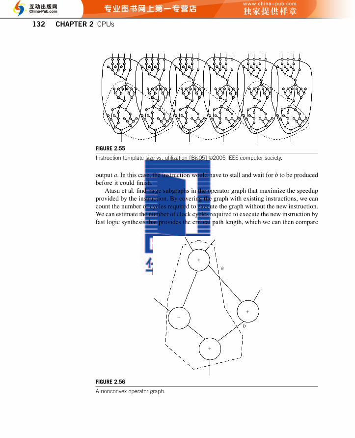
output a. In this case, the instruction would have to stall and wait for b to be producedbefore it could finish.
Atasu et al. find large subgraphs in the operator graph that maximize the speedupprovided by the instruction. By covering the graph with existing instructions, we cancount the number of cycles required to execute the graph without the new instruction.We can estimate the number of clock cycles required to execute the new instruction byfast logic synthesis that provides the critical path length, which we can then compare
FIGURE 2.55
Instruction template size vs. utilization [Bis05] ©2005 IEEE computer society.
a
b
+
+−
+
FIGURE 2.56
A nonconvex operator graph.
132 CHAPTER 2 CPUs

to the available cycle time. They use a branch-and-bound algorithm to identify cuts inthe operator graph that define new instruction subgraphs.
Biswas et al. [Bis05] use a version of the Kernighan-Lin partitioning algorithm tofind instructions. They point out that finding the maximum-size instruction does notalways result in the best result. In the example of Figure 2.56, the largest template,shown with the dotted line, can be used only three times in the computation, butthe smaller graph shown with the solid line can be used six times.
Sun et al. [Sun04] developed an instruction set synthesis system that used theTensilica Xtensa system to implement their choices. Their system generates TIEcode that can be used to synthesize processors. They generate instructions from pro-grams by combining microinstructions. They synthesize the register-transfer hard-ware for each candidate instruction, then synthesize logic and layout for thathardware to evaluate its performance and area. They select a subset of all possibleinstructions for further evaluation based upon their speedup and area potential.Based upon this set of candidate instructions, they select a combination of instruc-tions used to augment the processor instruction set. They use a branch-and-boundalgorithm to identify a combination of instructions that minimizes area while satis-fying the performance goal.
Pozzi and Ienne developed algorithms to extract large operations as instructions.Larger combinations of micro-operations provide greater speedups for many signal-processing algorithms. Because large blocks may require many memory accesses,they developed algorithms that generate multicycle operations from large data flowgraphs [Poz05]. They identify mappings that require more memory ports than areavailable in the register file and add pipelining registers and sequencing to performthe operations across multiple cycles.
Verma et al. developed an algorithm to optimize adder circuits [Ver09]. Theytransform ripple-carry adder structures to compressor tree structures (similar tothe Wallace tree adder) based on delay analysis. They define the rank of a circuitbased on its position in a carry chain: the rank of an adder carry output is oneplus the rank of its inputs; the rank of the sum output is the same as the rank ofits inputs; and the rank of all adder inputs are the same. The input signals of twofull adders are symmetric given two conditions: either the sum outputs of the fulladders are unused or there are paths from the full adders to another full adder viasum edges only; and the carry signals of all the full adders on the paths are symmet-ric. They find sets of symmetric signals and swap signals within each set to reducethe length of the critical delay path. They greedily swap signal pairs starting with theswap that maximizes the reduction in delay, stopping when no further reduction ispossible.
Athanasopoulos et al. developed methods to synthesize local memory, knownas architecturally visible storage (AVS), for custom instruction set extensions[Ath09]. They synthesize memory systems from a library of memory compo-nents, and formulate the data layout problem using Limited Improper Con-strained Color Assignment (LICCA); this problem is NP-complete. Theproblem is specified as a graph with nodes representing variables. Nodes are
Instructions in
combination
Large instructions
2.9 Automated CPU design 133
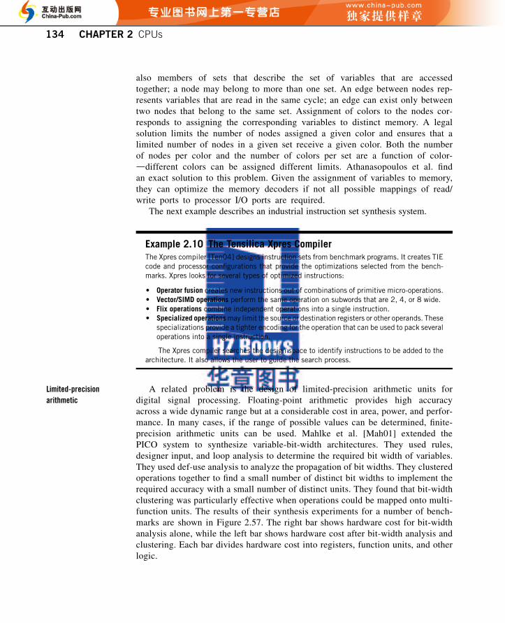
also members of sets that describe the set of variables that are accessedtogether; a node may belong to more than one set. An edge between nodes rep-resents variables that are read in the same cycle; an edge can exist only betweentwo nodes that belong to the same set. Assignment of colors to the nodes cor-responds to assigning the corresponding variables to distinct memory. A legalsolution limits the number of nodes assigned a given color and ensures that alimited number of nodes in a given set receive a given color. Both the numberof nodes per color and the number of colors per set are a function of color-ddifferent colors can be assigned different limits. Athanasopoulos et al. findan exact solution to this problem. Given the assignment of variables to memory,they can optimize the memory decoders if not all possible mappings of read/write ports to processor I/O ports are required.
The next example describes an industrial instruction set synthesis system.
Example 2.10 The Tensilica Xpres CompilerThe Xpres compiler [Ten04] designs instruction sets from benchmark programs. It creates TIEcode and processor configurations that provide the optimizations selected from the bench-marks. Xpres looks for several types of optimized instructions:
• Operator fusion creates new instructions out of combinations of primitive micro-operations.• Vector/SIMD operations perform the same operation on subwords that are 2, 4, or 8 wide.• Flix operations combine independent operations into a single instruction.• Specialized operationsmay limit the source or destination registers or other operands. These
specializations provide a tighter encoding for the operation that can be used to pack severaloperations into a single instruction.
The Xpres compiler searches the design space to identify instructions to be added to thearchitecture. It also allows the user to guide the search process.
A related problem is the design of limited-precision arithmetic units fordigital signal processing. Floating-point arithmetic provides high accuracyacross a wide dynamic range but at a considerable cost in area, power, and perfor-mance. In many cases, if the range of possible values can be determined, finite-precision arithmetic units can be used. Mahlke et al. [Mah01] extended thePICO system to synthesize variable-bit-width architectures. They used rules,designer input, and loop analysis to determine the required bit width of variables.They used def-use analysis to analyze the propagation of bit widths. They clusteredoperations together to find a small number of distinct bit widths to implement therequired accuracy with a small number of distinct units. They found that bit-widthclustering was particularly effective when operations could be mapped onto multi-function units. The results of their synthesis experiments for a number of bench-marks are shown in Figure 2.57. The right bar shows hardware cost for bit-widthanalysis alone, while the left bar shows hardware cost after bit-width analysis andclustering. Each bar divides hardware cost into registers, function units, and otherlogic.
Limited-precision
arithmetic
134 CHAPTER 2 CPUs

The traditional way to determine the dynamic range of an algorithm is by simula-tion, which requires careful design of the input data set as well as long run times. Fanget al. [Fan03] used affine arithmetic to analyze the numerical characteristics of algo-rithms. Affine arithmetic models the range of a variable as a linear equation. Terms inthe affine model can describe the correlation between the ranges of other variables;accurate analysis of correlations allows the dynamic range of variables to be tightlybounded.
2.10 SummaryCPUs are at the heart of embedded computing. CPUs may be selected from a catalogfor use or they may be custom-designed for the task at hand. A variety of architecturaltechniques are available to optimize CPUs for performance, power consumption, andcost; these techniques can be combined in a number of ways. Processors may bedesigned by hand; a variety of analysis and optimization techniques have been devel-oped to help designers customize processors.
0.9
0.8
0.6
0.5
0.4
0.3
0.2
0.1
0.7
0
Nor
mal
ized
cos
t
1
adpc
m cell
chai
nch
anne
lco
nv2d dct
edge
enco
de firise
dhe
athu
lfman
lines
cree
nlya
puno
rm
atm
ul rissh
arp
sobe
lta
ubvit
erbi
amea
n
FU Register Rest
FIGURE 2.57
Cost of bit-width clustering for multifunction units [Mah01] ©2001 IEEE.
2.10 Summary 135

What we learned• RISC and DSP approaches can be used in embedded CPUs. The design trade-offs
for embedded processors lead to some different conclusions than are typical forgeneral-purpose processors.
• A variety of parallel execution methods can be used; they must be matched to theparallelism available in the application.
• Embedded processors are prone to many attacks that are not realistic in desktop orserver systems.
• CPU simulation is an important tool for both processor design and softwareoptimization. Several techniques, varying in accuracy and speed, can be used tosimulate performance and energy consumption.
• CPUs can be designed to match the characteristics of the application for whichthey can be used. The instruction set, memory hierarchy, and other subsystems canall be specialized to the task at hand.
Further readingConte [Con92] describes both CPU simulation and its uses in computer design. Fisheret al. [Fis05] provides a detailed analysis of VLIW architectures for embeddedcomputing. The chapter by Rotenberg and Anantararaman [Rot04] provides an excel-lent introduction to embedded CPU architectures. This chapter has made reference toUnited States Patents; U.S. Patents are available online at http://www.uspto.gov.
QuestionsQ2-1 What are the basic characteristics of a digital signal processor?
Q2-2 Compare and contrast superscalar and VLIW execution.
Q2-3 Why might vector units be useful in embedded processors?
Q2-4 Draw a chart comparing the characteristics of several types of processors(RISC, DSP, VLIW, GPU) with regard to several application characteristics(flexibility, energy, performance).
Q2-5 What property of multimedia applications limits the available instruction-level parallelism?
Q2-6 Identify possible instructions in matrix multiplication.
Q2-7 Identify possible instructions in the fast Fourier transform.
Q2-8 Compare and contrast performing a matrix multiplication using subwordparallel instructions and vector instructions. How do the code fragments forthe two approaches differ? How do these differences affect performance?
136 CHAPTER 2 CPUs

Q2-9 Compare the opportunities for parallelism in a Viterbi decoder. Would asuperscalar CPU be able to find much more parallelism in a Viterbi decoderthan would be found by a VLIW compiler?
Q2-10 Identify the components in a memory block that contribute to the compo-nents of the memory block delay model.
Q2-11 Build a model for a two-way set-associative cache. The parameters of thecache are line size l (in bits) and number of lines n. Show the block-levelorganization of the cache. Create formulas describing the area A, delayD, and energy E of the cache based upon the formulas for the block-levelmodel.
Q2-12 Evaluate cache configurations for several block motion estimation algo-rithms. The motion estimation search uses a 16 � 16 macroblock and asearch area of 25 � 25. Each pixel is 8 bits wide. Consider full search andthree-step search. The cache size is fixed at 4096 bytes. Evaluate direct-mapped, two-way, and four-way set-associative caches at three differentline widths: 4 bytes, 8 bytes, and 16 bytes. Compute the cache miss ratefor each case.
Q2-13 Based on the data of Wehmeyer et al., what size register file provides goodperformance for most applications?
Q2-14 Why does code compression need to use branch tables? Do branch tablesrestrict the type of code that can be executed in the compressed codesystem?
Q2-15 Evaluate the energy savings of bus-invert coding on the address bus for theaddress sequences to the array a[10][10], where a starts at address 100.Changing one bit of the address bus consumes e energy. Give the totalsavings for bus-invert coding versus an unencoded bus.a. Row-major sequential accesses to the array a.b. Column-major sequential access to a.c. Diagonal accesses such as those used for JPEG DCTencoding (0,0 -> 1,0
-> 0,1 -> 2,0 -> 1,1 -> 0,2 -> ...).
Q2-16 How do branches affect the effectiveness of bus-invert coding?
Q2-17 How would you determine the proper dictionary size for a dictionary-basedbus encoder?
Q2-18 Illustrate the operation of Lempel-Ziv encoding on the string abcabd.
Q2-19 You are designing a configurable CPU for an embedded application. Howwould you choose the cache size and configuration?
Q2-20 Write TIE code for a multiply-accumulate instruction: acc ¼ acc þ a * b.
Q2-21 Design an algorithm to find convex subgraphs in an operator graph.
Questions 137

Lab exercisesL2-1 Develop a SimpleScalar model for a DSP with a Harvard architecture and
multiply-accumulate instruction.
L2-2 Use your SimpleScalar model to compare the performance of a matrixmultiplication routine with and without the multiply-accumulate instruction.
L2-3 Use simulation tools to analyze the effects of register file size on the perfor-mance of motion estimation. Compare full search and three-step search.
138 CHAPTER 2 CPUs