chapter 8 - center for environmental implications of nanotechnology
TRANSCRIPT

284
CHAPTER 8
APPLICATIONS: NANOELECTRONICS AND NANOMAGNETICS
Jeffrey Welser, Stu Wolf, Phaedon Avouris, Tom Theis31
8.1 VISION FOR THE NEXT DECADE
Changes in the Vision over the Last Ten Years
In the last ten years, the state of the art in nanoelectronics, including nanomagnetics, has rapidly gone from devices at or above 100 nm in size to the realm of 30 nm and below, with a well-defined pathway to devices (including transistors for logic and memory) of about 15 nm. In the process of reaching this size, the thickness of the critical layers in many structures is approaching 1 nm; the threshold voltage of a metal-oxide semiconductor field effect transistor (MOSFET) device is now controlled by fewer than 100 atoms, and the line edge roughness requirements are a few nanometers. All of these advances have resulted in an increased demand for near-atomic-level control for deposition, patterning, and characterization.
Vision for the Next Ten Years
In the coming decade the research community must focus on what happens at 10 nm and below for all devices. Moreover, there needs to be an increased focus on how to utilize the new physics offered at the nanoscale to increase device functionality. It is ironic that in the past 10 years, nanoelectronics has arguably been the primary driver (both economically and technologically) for increasing our ability to control material at the nanoscale, but the nanoelectronics community has largely used these increasing capabilities to shrink existing devices while attempting to maintain the microscale physics that has enabled exponential progress in miniaturization for the past half century. In the sub-10 nm world, there will be no choice but to embrace the new nanoscale phenomena and focus on how to utilize them for new functionality beyond the complementary metal oxide semiconductor (CMOS) device. This will not only mean taking advantage of new nanoelectronic phenomena, but increasingly it will also mean manipulating the magnetic, spintronic, and other properties of matter at the nanoscale as state variables for computation and new forms of data storage. Moreover, this new functionality will not only improve our existing products, but it will open up new application areas, including new sensors, new ultralow power devices, and new flexible electronics. The result will be ever more ubiquitous applications of semiconductor nanoelectronics—beyond those in today’s laptops and cell phones and those that are an increasingly integral part of appliances, cars, homes, and healthcare—in products and industries yet to be conceived by a new generation of entrepreneurs.
31For the institutional affiliations of authors, please see Appendix B, List of Participants and Contributors.
J. Welser, S. Wolf, P. Avouris, T. Theis
285
The expansion of nanoelectronic application areas will require an increased focus on research that considers from the beginning not just the device, but the circuit, architecture, and end application, as well as the societal implications of devices that may be embedded in our everyday world. While focused research on new materials and new scientific phenomena for novel devices will clearly need to continue, there will also be a shift toward increased research on nanosystems that not only takes advantage of the properties of the devices but also considers how to exploit the novel interactions between multiple devices in new architectures. This will drive an increased need for design tools and methodologies that can bridge from the materials level to the system level, as well as drive increased interaction between researchers in the basic sciences and those focused on applications. Hence, the next 10 years will see even more need for multidisciplinary teams to do the nanoelectronic and nanomagnetic research for the future.
8.2 ADVANCES IN THE LAST TEN YEARS, AND CURRENT STATUS
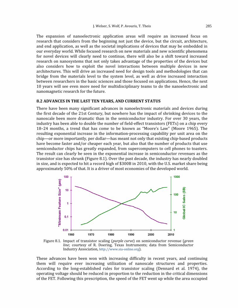
There have been many significant advances in nanoelectronic materials and devices during the first decade of the 21st Century, but nowhere has the impact of shrinking devices to the nanoscale been more dramatic than in the semiconductor industry. For over 30 years, the industry has been able to double the number of field-effect transistors (FETs) on a chip every 18–24 months, a trend that has come to be known as “Moore’s Law” (Moore 1965). The resulting exponential increase in the information-processing capability per unit area on the chip—or more importantly, per dollar—has meant not only that existing chip-based products have become faster and/or cheaper each year, but also that the number of products that use semiconductor chips has greatly expanded, from supercomputers to cell phones to toasters. The result can clearly be seen in the exponential increase in semiconductor revenues as the transistor size has shrunk (Figure 8.1). Over the past decade, the industry has nearly doubled in size, and is expected to hit a record high of $300B in 2010, with the U.S. market share being approximately 50% of that. It is a driver of most economies of the developed world.
Figure 8.1. Impact of transistor scaling (purple curve) on semiconductor revenue (green
line; courtesy of R. Doering, Texas Instruments; data from Semiconductor Industry Association, http://www.sia-online.org).
These advances have been won with increasing difficulty in recent years, and continuing them will require ever increasing utilization of nanoscale structures and properties. According to the long-established rules for transistor scaling (Dennard et al. 1974), the operating voltage should be reduced in proportion to the reduction in the critical dimensions of the FET. Following this prescription, the speed of the FET went up while the area occupied

8. Applications: Nanoelectronics and Nanomagnetics
286
by the device and power used by the device went down, so that the areal power density remained constant. In the past 10 years, as devices shrank below 100 nm in gate length, the rule governing reduction of voltage had to be abandoned, primarily because a minimum gate voltage swing is necessary to switch an FET from an “off” (low-current) state to an “on” (high-current) state. If that swing is too small, the device will have excessive leakage current (high passive power dissipation) in the nominally “off” state or low current (slow circuits) in the nominally “on” state. While it seems that devices can continue to be shrunk for the next 5–10 years, the designs utilizing them must increasingly trade density for speed in order to mitigate the increasing on-chip power density (Frank 2002). This will in limit the ability of further size reduction to achieve the full historical benefits of increasing computation/second/dollar/watt that has driven the industry up to now. Moreover, while the power-density challenge is affecting all applications (including large servers in datacenter environments), the overall energy consumption is even more problematic for the increasing number of mobile devices. These require not only finding a device with low operation energy, but also ultra-low (or zero) passive and standby energy needs. The trade-off between performance and leakage current is especially difficult in these applications, and finding novel non-volatile devices—potentially even for the logic devices—would offer major advantages. In addition, finding ultra-low power transistors not only increases traditional battery life, but opens the door to more exotic energy scavenging techniques to power these devices in the future.
In addition, as FETs have been shrunk to the tens of nanometers size range, rather than benefiting from new phenomena at the nanoscale, their performance has been challenged by increases in tunneling currents and the need for almost atomic-scale precision in fabrication. At the 90 nm node in the first part of the decade, for example, the gate insulator was approaching 1.5 nm in thickness—just a few atomic layers of silicon oxy-nitride—which not only resulted in unacceptably high tunneling leakage currents but also required monolayer control across a 200 mm wafer. The solution was to introduce an insulator with higher dielectric constant, which allowed for an increased thickness but in most cases also required changing the gate electrode process to a combination of polysilicon and metal (Lee et al. 2008). The result was decreased electrical thickness, which allowed further shrinking of the gate length. However, even with high-K material, the insulator thickness is still only a few nanometers, and with a lowered barrier height. Further improvements in gate dielectric materials will probably be limited, and therefore further reduction of gate length may depend on introduction of new device structures as discussed below.
The gate length for modern transistors is now about 30 nm. This is exceedingly difficult to achieve with current optical lithography, which utilizes 193 nm wavelength light to pattern the features. It is only possible through many tricks, including chemically active resists, restricted design rules, extensive use of optical proximity correction on the masks, and most recently, the introduction of immersion techniques to reduce the effective refractive index for the exposure (Sivakumar 2006). Moreover, since many of the electrical properties of the FET are exponentially dependent on gate length (including leakage currents), these dimensions must be controlled to just a few nanometers. Variations in line width across a wafer, and increasingly across a single die, are one of the major sources of variability that limit ultimate chip yield and performance, so it is crucial that new patterning solutions are found. The current approach for the industry is to push optical lithography to the extreme ultraviolet (EUV) range, but this continues to be a huge challenge, largely in finding suitable mask and resist materials (Wu and Kumar 2007), and significant research in this area is still required. Beyond optical lithography, emerging patterning processes such as nanoimprint lithography

J. Welser, S. Wolf, P. Avouris, T. Theis
287
(Schift 2008), scanning probe lithography (Pires et al. 2010), and various forms of self-assembly (Lu and Sastry 2008; Craig and Nealey 2007) are being explored. These are key areas of research for the coming decade.
It is important to note that both the gate oxide and lithography improvements were only possible due to the research in nanoscale fabrication and characterization that has taken place over the past 10 years. Continued scaling will require further fundamental advances in lithographic and other processes for precise fabrication of nanometer-scale structures. Advances in metrology will be necessary to attain the required precision. Furthermore, future devices must take direct advantage of nanoscale effects as well. One interesting example that has already reached the market is the use of nanocrystal floating gates (Tiwari et al. 1995) for nonvolatile FLASH memory (Chang 2006; Freescale Semiconductor 2010). Utilizing nanocrystals rather than continuous floating gates for storing charge should allow the use of thinner insulators and improve the scaling potential for future FLASH devices. Recent advances in nanoscale materials and device physics are also behind rapid progress in two other non-volatile memory devices that are entering the commercial arena. Phase Change Memory (PCM) has been in development for decades and is now considered to be a potential successor to silicon FLASH memory because of its superior potential to be scaled to small size. Extensive materials research shows that the phase change behavior is well defined in films as thin as 1 nanometer and exploratory device research suggests that devices with active material volumes of just a few cubic nanometers are feasible (Burr et al. 2010). Looking forward, advances in the understanding of oxygen vacancy transport in metal oxides and other effects which can induce resistance changes in material stacks may find potential application in other resistive memory devices, including novel “memristor” devices (Strukov et al. 2008; Yang et al. 2008; Chua 1971), that may be useful in memory (Vontobel et al. 2009), storage, and even circuits which mimic the synaptic function of the brain (Borghetti et al. 2009, 2010). The other emerging non-volatile memory technology is Magnetic Random Access Memory (MRAM). It has been in commercial development since the mid-nineties, and promises much greater speed, lower power, and far better durability than either FLASH memory or PCM. However, a path to very small devices became evident only after a scientific breakthrough—the experimental demonstration of the spin-torque transfer effect (Katine et al. 2000). See the discussion below of Nanomagnetics and Spintronics.
For FETs used in digital logic circuits, the most promising directions forward involve reduced-dimension structures, starting with ultrathin silicon-on-insulator (SOI) and double-gate or FinFET devices (Jurczak et al. 2009), ultimately leading to completely 1D structures such as nanowires (Lu 2009) and nanotubes (Avouris et al. 2003). All of these structures enable improved gate control of the FET channel current, allowing shorter channels and better performance. Carbon nanotubes (CNTs) in particular have been studied intensely for this over the past 10 years, and many interesting demonstrations have been done that take advantage of their high carrier mobility, high thermal conductivity, and unique physics (Avouris et al. 2003). The key remaining obstacle to the use of nanotubes and nanowires in high performance electronics is the lack of fabrication methods that allow dense packing of uniform diameter tubes/wires across a large area with low defects and identical electrical behavior. For flexible electronics or applications that currently utilize thin film transistors (TFTs), the requirements are greatly relaxed. Hence the first large-scale application of CNTs may be as a mesh structure for moderate-performance flexible electronics—an area of growing importance in the future.
Regardless of the material or structure used, all of the above-mentioned FETs are approaching some hard limits due to the basic physics of the device operation. Thus there is a

8. Applications: Nanoelectronics and Nanomagnetics
288
strong need to explore new device concepts that circumvent these limitations. Similar motivations drove the development of both the first solid state transistors, based on bipolar technology, when vacuum tubes and mechanical switches were reaching similar power constraints in the late 1940s, and the current FET, which replaced bipolar transistors in the majority of semiconductor applications in the late 1980s. The potential for yet another major device transition was recognized at the beginning of the decade, and the Semiconductor Research Corporation (SRC) and the National Science Foundation (NSF) jointly organized a set of industry-academia-government workshops (Cavin and Zhirnov 2004; Cavin et al. 2005; Cavin et al. 2006) to study the problem. In parallel, the Technology Strategy Committee of the Semiconductor Industry Association (SIA) conducted several workshops whose objective was to identify research initiatives to advance integrated circuit technology beyond currently identified scaling limits. These activities ultimately defined key research vectors considered to be important components of the search for the next switch and resulted in the formation of the Nanoelectronics Research Initiative (NRI, http://nri.src.org) by the SIA in 2005. Managed by the SRC, the NRI’s mission is to demonstrate novel computing devices capable of replacing the CMOS FET as a logic switch in the 2020 timeframe. These devices must show significant advantage over ultimate FETs in power, performance, density, and/or cost, and most importantly must enable the semiconductor industry to extend the historical cost and performance trends for information technology (Welser et al. 2008).
The NRI’s primary goal is to circumvent the power density issues that are currently limiting CMOS technology. To go beyond this limit, the physics of the device or the mode of its operation must be fundamentally changed so that much less energy is dissipated in each switching operation. To accomplish this, the primary focus is on switches that utilize alternative state variables to represent information (compared to the FET, which relies on the dissipative movement of charge), as well as on the corresponding interconnects and circuits needed to perform logic. Research is also being done on nanoscale phonon engineering, both to manage heat and potentially to isolate systems from thermal noise, and on directed self-assembly of key device structures. The challenge—and urgency—of finding a new switch to enable continued progress in nanoelectronics beyond 2020, similar to what has driven the economy for the past half century, should not be underestimated and should be one of the primary foci of nanoelectronics work in the coming decade.
While many of the nanoelectronic advances in the past decade have already had impact on mainstream electronics, many other breakthroughs show great promise for new innovations in the coming decade. A few examples include:
• The discovery of graphene and development of methods for controlled growth or synthesis (Novoselov et al. 2004).
• Elucidation of the electronic, optical and thermal properties of carbon nanotubes and graphene and establishment of a new class of electronic materials – carbon electronics.
• Discovery of magnetoelectric and multiferroic materials which promise voltage-control of magnetism (Wang et al. 2003).
• The experimental realization of spin torque switching (Katine et al. 2000). • Discovery of the Spin Hall Effect (Dyakonov and Perel 1971; Kato et al. 2004; Wunderlich
et al. 2005). • Demonstrations of spin injection into and spin readout from semiconductors. • The discovery of topological insulators, a new and topologically distinct electronic state in
matter with unique collective transport properties (Bernevig et al. 2006; Koenig et al. 2007; Chen et al. 2009).

J. Welser, S. Wolf, P. Avouris, T. Theis
289
• Advances in the understanding and development of dilute magnetic semiconductors (Ohno et al. 1996; Dietl et al. 2000).
• Fundamental understanding of the chemistry and physics of semiconductor nanowire growth.
• The exploration of nanoscale solid-state electrochemistry for a variety of potential applications in device technology (Terabe et al. 2005).
• Some of these breakthroughs have already developed into major new fields of technology exploration, with two of the largest areas currently being graphene electronics and spintronics.
Graphene Electronics
One of the most interesting developments for future nanoelectronics has been the rediscovery of graphene—a single monolayer of graphitic carbon—as a potential substrate with unique physics. This material has almost all of the same advantages of CNTs (as well as other attributes), but it is a planar material, making device fabrication more straightforward. However, producing the initial substrate of graphene is still very challenging. While the electronic structure of graphene was calculated back in 1945 (Wallace 1947), and ways to produce graphene on metals (May 1969), SiC (Van Bommel, Crombeen, and Van Tooren 1975), and graphene oxide (Boem et al. 1962) were demonstrated early on, research on the electronic properties of graphene did not start earnestly until 2004, when single-layer graphene was exfoliated from graphite and deposited on SiO2 (Novoselov et al. 2004). Early experimental and theoretical work was focused on the 2D electron gas properties, particularly on the study of graphene’s quantum Hall effect (Novoselov et al. 2005; Zhang et al. 2005) and its minimum conductivity (Geim and Novoselov 2007). Transport measurements firmly established its excellent electrical properties: mean-free paths of hundreds of nanometers to a micrometer and mobilities of the order of 10,000 cm2/Vs in the supported state and over 200,000 cm2/Vs in the suspended state (Geim and Novoselov 2007; Bolotin et al. 2008). Additionally, graphene possesses extremely high current-carrying capability and excellent thermal conductivity and mechanical strength.
Graphene was incorporated early on as the channel of field-effect transistors, and the device current could be modestly modulated by the gate field due to the linear variation of the graphene density-of-states with energy (Geim 2009). However, because of the lack of a bandgap (graphene is a zero bandgap semiconductor), the achieved current on/off ratios have been, in general, below 10. Thus, although, graphene was hailed in the popular press as a successor to Si-MOSFETs, the lack of a bandgap currently precludes its use in digital electronics. On the other hand, in bilayer graphene with the layers stacked in the so-called AB or Bernal stacking configuration, the interaction between the two layers was shown theoretically in 2006 to lead to the opening of a bandgap on application of a strong vertical electrical field (McCann 2006). Early experiments failed to reveal a significant bandgap opening (Oostinga et al. 2008), most likely because of the quality of the bilayer sample used. In more recent experiments using a better dielectric gate stack, the opening of an electrical bandgap >140 meV was demonstrated (Xia et al. 2010), and further improvements are expected.
The initial graphene experiments were performed using exfoliated graphite. Soon, however, synthetic techniques for growing monolayer and multilayer graphenes appeared. Currently, the key synthetic techniques involve the thermal decomposition of SiC (Berger et al. 2004) and chemical vapor deposition on metals such as Ni (Reina et al. 2009) or Cu (Li et al. 2009).

8. Applications: Nanoelectronics and Nanomagnetics
290
While digital electronic applications are not currently possible for graphene, its extremely high carrier mobility at room temperature, ultimate body thinness, high transconductance, and modest field tuning of the current recommend graphene for high-frequency analog electronic applications. In particular, radio-frequency field-effect transistors (RF-FETs) could find use in wireless communications, radar, security and medical imaging, vehicle navigation systems, and a host of other applications. Currently, the record cutoff frequency (fT) achieved by RF graphene transistors based on exfoliated graphite stands at 50 GHz (Lin, Chiu et al. 2010 ). Of course, for commercial applications, wafer-scale graphene is required. This can be achieved using the above-mentioned graphene synthetic techniques. In particular, the SiC-based approach has yielded wafer-sized samples of graphene. Graphene wafers from the Si-face of SiC show good layer thickness control and morphology and have mobilities that currently are in the range of 1,000 to 3,000 cm2/Vs. C-face SiC yields graphene with higher mobilities but with thicker layers and less controlled morphology. RF transistors have been fabricated on Si-face SiC-derived 2-inch graphene wafers (Lin, Chiu et al. 2010; Moon et al. 2009). The current record involves 240 nm gate length transistors from IBM with cutoff frequencies of 100 GHz (Lin, Dimitrakopoulos et al. 2010). This is already remarkable since Si-CMOS transistors with the same gate length achieve cutoff frequencies of 40 GHz. The currently achieved fT x (gate length) product of 22 GHz ∙ µm is higher than that of most semiconductors, and both scaling of the devices and improvements in the graphene mobility are expected to yield much higher-frequency performance (Figure 8.2).
Another possible area for applications of graphene that can utilize its exceptional transport properties for both electrons and holes, as well as its strong optical absorption over a very wide wavelength range (about 2% per atomic layer), is optoelectronics. Ultrafast (>40 GHz) metal-graphene-metal photodetectors have been demonstrated (Xia et al. 2009), and these photodetectors have been used recently to detect reliably optical data streams at 10 Gbits/s (Mueller et al. 2010). THz radiation emitters from monolayer and bilayer graphene are also very likely to emerge soon.
Finally, beyond the traditional electron transport and optical devices, the physics of graphene could offer new possibilities for devices with unique functionality. The two-dimensional honeycomb lattice of graphene gives rise to a conical band structure, which leads to electrons behaving as massless Dirac fermions. Some proposed devices take advantage of the resulting photon-like behavior of electrons in graphene and utilize p-n junctions to create programmable interconnects or Veselago lens devices (Chelanov, Fal’ko, and Altshuler 2007).
A completely different approach is taken by another new transistor concept, the bilayer pseudospin FET (BiSFET) (Banerjee et al. 2009). In this device, two metal oxide gates sandwich two separately contacted graphene monolayers separated by a tunnel oxide. This device takes advantage of the pseudospin property (Min et al. 2008), which predicts that under certain gate conditions an exciton condensate forms between the graphene layers, leading to the possibility of a collective many-body current between the two layers (Su and MacDonald 2008). This could potentially enable a very low-energy switch, even at room temperature (Banerjee et al. 2009).

J. Welser, S. Wolf, P. Avouris, T. Theis
291
Figure 8.2. (A) Scanning electron microscope image and the schematic cross-sectional
view of a top-gated graphene field-effect transistor. The optical image of the two-inch graphene/SiC wafer with arrays of graphene devices is on the right. The transistors possess dual-gate channels to increase the drive current and lower the gate resistance. The scale bar is 2 µm. (B) Drain current ID of a 240-nm gate length graphene transistor as a function of gate voltage VG at drain bias of 1 V. The current shown was normalized with respect to the total channel width. The device conductance gm = dID/dVG is shown on the right axis. (C) Measured drain current ID as a function of drain bias of a graphene FET with a gate length Lg of 240 nm for various top-gate voltages. (D) Measured small signal current gain |h21| as a function of frequency f for a 240-nm gate and a 550-nm gate graphene FET, represented by () and (), respectively. The current gain for both devices exhibits 1/f dependence, where a well-defined cutoff frequency fT can be determined to be 53 GHz and 100 GHz for the 550-nm and 240-nm devices, respectively (Lin, Dimitrakopoulos et al. 2010).
Nanomagnetics and Spintronics
While electronics and semiconductors have traditionally formed the basis for the chip industry, magnetics has formed the basis for the storage industry. During the past 10 years, though, advances in nanometer-sized magnetic devices as well as new methods for
8. Applications: Nanoelectronics and Nanomagnetics
292
controlling spin properties in general have enabled increased usage of nanomagnetics, including on chip. There have been significant advances in spintronics, particularly in areas based on a nanoscale multilayer structure, that is, a magnetic tunnel junction (MTJ) (Moodera et al. 1995; Miyazaki and Tezuka 1995). Magnetic tunnel junctions are already ubiquitous in that they are the key component in the sensor that reads the information stored on a magnetic disk. In 2006, a new type of nonvolatile, infinite-endurance computer memory was introduced to the marketplace called magnetic random access memory or MRAM (Tehrani et al. 1999). This memory is now manufactured and sold by a spinoff of Freescale Semiconductor called Everspin, which has been introducing MRAM into more and more markets over the last few years. MRAM is also going to be a key component in defense systems that require radiation-hard, nonvolatile memory; Honeywell has teamed with Everspin to provide just such a product that is now going into production. The MTJ can also be used as a sensor, and this has found several applications in industrial sensing as well as in cell phones to provide directional information (a 3D magnetic compass).
Several key discoveries led to the successful development of MRAM, including a novel method of switching the bit, called toggle-switching (Engel et al. 2005), and the discovery of a new tunnel barrier (MgO) that enabled an order-of-magnitude increase in the tunneling magnetoresistive ratio (TMR) (Butler et al. 2001). In the beginning of the last decade, another major hurdle for MRAM was overcome with the discovery of magnetization reversal due to scattering of a spin-polarized current (Katine et al. 2000). This discovery, called spin torque transfer (ST or STT) switching, will allow MRAM to scale to well under 10 nanometers, dimensions that traditional switching methods using current-generated magnetic fields will never allow. Spin torque transfer also enables the generation of spin wave radiation due to the rapidly precessing magnetization of the “free layer” of a tunnel junction in a magnetic field. These nano-oscillators may find many uses in signal generation and processing as well as in phased arrays for RF detection and radiation. Finally, spin torque transfer provides a means to move magnetic domain walls in a magnetic nanowire (Parkin, Hayashi, and Thomas 2008). This provides an alternate path for information storage and perhaps even processing. Prior to the discovery of spin torque transfer, magnetic domain walls were moved using changing magnetic fields, which are cumbersome and power-hungry.
Another major direction for spintronics was enabled by the realization that traditional semiconductors could be made magnetic by adding dilute amounts of magnetic ions, particularly manganese (Wolf et al. 2001). These materials, by virtue of the fact that in most cases the magnetism is mediated by carriers—and carrier concentrations can be controlled electrically—offer the unprecedented ability for the magnetism to be controlled with an electric field. The field of semiconductor spintronics has grown exponentially in the last decade but has been hindered by the absence of a magnetic semiconductor with a Curie temperature well above room temperature. However, proof-of-principle demonstrations of various spin-injection and FET-like devices show that if the right material is found, then adding the spin degree of freedom to semiconducting devices will enable a broad spectrum of applications spanning many diverse fields of electronics and photonics (Wolf et al. 2001).

J. Welser, S. Wolf, P. Avouris, T. Theis
293
8.3 GOALS, BARRIERS, AND SOLUTIONS FOR THE NEXT 5–10 YEARS
While there are many fruitful areas to be explored in nanoelectronics in the next 10 years, six primary goals and directions are highlighted as particularly important in the areas of fabrication, devices, and architectures, as described below.
Fabrication: Achieve 3D Near-Atomic-Level Control of Reduced Dimensional Materials
This includes not only the growth of nanotubes and nanowires with control of diameter, chirality, and placement across a wafer, but also the growth of large-area monolayer (or multilayer) graphene. It also includes the production of layered structures and interfaces, key to some emerging areas like topological insulators, multiferroic materials, and complex metal oxides, as well as more complex structures such as lattices of ferroelectric material with embedded ferromagnetic particles to create artificial magneto-electric structures. While there are specific barriers involved with different materials, all of these require increased control of both thickness and lateral dimensions during growth and/or etching, as well as metrology tools with sufficient resolution in multiple dimensions to measure the structures. It also requires continued advances in predictive modeling of materials to guide the design of new materials and interfaces with unique functionality.
Fabrication: Combine Lithography and Self-Assembly to Pattern Semi-Arbitrary Structures Down to 1 nm Precision
While self-assembly can potentially offer solutions for creating exceedingly small patterns, the number of defects is currently too high to be useful for most applications, and simple self-assembly processes can only produce repetitive structures. Defect rates in self-assembly must be improved, and efficient mechanisms for integrating self-assembly with lithographic patterning (templated self-assembly) must be developed to allow arbitrary pattern formation (Saavedra et al. 2010). Given the current rate and pace of scaling, 1-nm precision will soon be necessary for fabrication of devices in complex circuits and systems. It is very important, therefore, to continue research investments in the science and engineering of precision patterning. At the same time, architectures and circuits must also evolve to work with imperfect structures and more regular layouts of devices. More communication between the various research areas will be necessary to achieve balance.
Devices: Discover Devices for Logic and Memory that Operate with Greatly Reduced Energy Dissipation
Power is the key barrier to continuing scaling of almost all nanoelectronic devices, so finding devices that can operate at room temperature with as little energy dissipation as possible is imperative. Logic devices are particularly challenging, since they must maintain adequate speed to allow continued scaling of overall computation / second / area / watt. It is unlikely this can be achieved solely through geometric scaling of the FET, as has been done in the past, so the focus must be on devices and device concepts that maintain distinguishability of logic state with less stored energy than the FET, or on devices that can do more complex functions and/or multibit calculations at a given energy dissipation and area. Beyond the speed consideration, the biggest barrier to low-energy devices of any kind is robustness to thermal noise. To address these challenges, collective effects and alternative state variables must be considered for future device candidates. This means finding new methods of representing information with material properties or parameters that can be manipulated into distinguishable states. Condensed matter theory offers many materials with broken symmetries that result in distinguishable regions characterized by different order

8. Applications: Nanoelectronics and Nanomagnetics
294
parameters. These include ferroelectric, antiferroelectric, ferromagnetic, antiferromagnetic, ferrotorodic, ferroelastic, and ferrimagnetic materials, among others (Eerenstein, Mathur, and Scott 2006). In many cases, these order parameters are coupled together by the atomic structure of the crystalline lattice structure. Examples of order coupling include magnetoelectric, piezoelectric, piezomagnetic, electrostrictive, and magnetostrictive effects. The key is to identify which of these can be manipulated at reasonable speed at low energy—while remaining thermally robust—to do computations at room temperature. In addition, consideration must also be given to the using these devices in circuits that can operate out of equilibrium with the ambient for a period of time or that can recover the switching energy as part of the computation cycle. This leads to the need for research also in the area of phonon engineering, to better control thermal interactions with nanodevices. Finally, for mobile applications, it’s important to pay particular attention to reducing (or eliminating) standby power and leakage, potentially with non-volatile device solutions.
Devices: Exploit Spin for Memory, Logic, and New Functionality
While many potential state variables should be explored, an area that is particularly ripe for exploitation over the coming decade is spintronics. Spin and magnetics have already proven valuable for storage devices and increasingly are showing promise for memory, but they offer many other potential opportunities in sensors, oscillators, and logic devices as well. Finding energy-efficient ways to manipulate spin—potentially with electric fields using multiferroic and dilute magnetic semiconductor materials—is imperative to this, as is studying the behavior of both single-spin and collective-spin states. This requires advances both in the materials and in the characterization tools for measuring individual spins and nanoscale magnets—and in particular, the dynamics of their behavior in novel materials.
Architecture: Integrate Architecture and Nanoscale Device Research for Unique Computation Functionality
While the past 10 years have largely seen demonstrations of individual nanoelectronic devices and new science phenomena, the next 10 must focus on how these are integrated on a large scale and how they can be used to perform a useful function. For integration, that includes research on large-scale, reproducible fabrication of nanostructures; interconnects—potentially non-charge-based—between devices (and the impact they have on power and speed); consideration of nanostructure-environment and nanostructure-nanostructure interactions; and dealing with stochastic processes, noise, and thermal management. On the function side, rather than forcing new devices to fit into the current charge-based, Boolean systems, architecture researchers should look for novel architectures to take advantage of the unique functionality of a given device to implement important algorithms or applications, such as pattern matching, fast Fourier transform (FFT) computation, encryption, etc. In particular, they should consider how to work with the realities of most nanoscale devices (e.g., dense, slow, sea-of-gate structures with high levels of defects) while taking advantage of some of their assets (e.g., the prospect of merging memory and logic or making programmable architectures by taking advantage of the nonvolatile switches). Conversely, architects should also be thinking abstractly about entirely different approaches to doing even general-purpose computation, with a particular eye towards stochastic or “almost-right” computation, and giving feedback to device researchers on what kind of functionality would be needed in a new device to enable implementation of the architecture.

J. Welser, S. Wolf, P. Avouris, T. Theis
295
Architecture: Increase Focus on Emerging, Non-IT Applications
The major future market for electronics is likely to be outside of the traditional information technology (IT) space and instead geared for embedded applications in vehicles, appliances, homes, and even human bodies. Yet the research is still largely focused on traditional computer chip applications. Breakthroughs in the areas of low-power devices, sensors, transmitters, receivers, and flexible substrates are key components for these embedded applications, and to enable this, more research is needed on nanostructures specifically. At the same time, an increased emphasis is needed on understanding the environmental impacts of nanoelectronic components as they become more ubiquitous. Since each of these non-IT applications has unique requirements (e.g., high temperature, ultra-low power, biologically friendly packaging, etc.) it is important that research be more focused on the final application from the beginning, rather than just on the general problem of improving computation or memory in traditional environments.
8.4 SCIENTIFIC AND TECHNOLOGICAL INFRASTRUCTURE NEEDS
The primary need to enable the nanoelectronic and nanomagnetic research necessary to achieve the goals listed in Section 8.3 is readily accessible tools—at low cost—to fabricate, characterize, and model active structures at the atomic scale. For fabrication, the ability to pattern reliably down to the 1 nm scale is crucial and will likely require a combination of tools for integrating both top-down (lithographic) and bottom-up (self-assembly) techniques. For characterization, the primary needs are for tools that can measure static structures (vertically and laterally) down to an atomic layer, as well as tools that can characterize the growth and patterning of these structures in situ to enable better understanding and control of the dynamics of the material growth. In addition, the ability to characterize the dynamics of single-carrier transport, spin precession, magnetic and ferroelectric domain reorientation, and a host of other material state transitions will become increasingly important as alternative state variables are explored. For modeling, an increased focus on tools that can scale-up atomic, first-principles simulations to macroscopic, device- (and circuit-) relevant structures is a major goal. Finally, the infrastructure and tools development for these areas should focus not only on tools that can accomplish this resolution for “single devices” in a research lab, but also on tools that enable the scale-up of the work to the “billion devices” needed for cost-effective nanomanufacturing. And this is not limited to just scaling up the fabrication tools, but also finding efficient, noninvasive characterization techniques for key parameters to use in monitoring and controlling inline manufacturing processes, and developing multiscale modeling tools that can facilitate rapid device and circuit design for product development while not sacrificing accuracy.
Although the number of materials being incorporated expands every year, the majority are still inorganic semiconductors, metals, and insulators, including an increasing number of ferroelectric, ferromagnetic, and even multiferroic materials. Therefore, the required tools are similar to what is already available in the national nanofabrication and characterization facilities, both at universities and at NIST and the DOE national laboratory user facilities. The National Nanotechnology Infrastructure Network (NNIN; http://www.nnin.org/) is a good model for this, but it needs to be greatly expanded both in terms of the number of facilities it supports across the country as well as in terms of updating the tools themselves. The NNIN facilities were largely built in the 1980s and 1990s for the microelectronic generations, so they aren’t necessarily suitable for the nanoelectronics era. In addition, the current NNIN model, which largely invests only in the initial tool purchase and relies on user fees to cover the operations costs, is not practical for many of the modern tools. Many of these tools can

8. Applications: Nanoelectronics and Nanomagnetics
296
cost upwards of $5–10 million, and typical warranty costs are 10% of the tool cost per year; in addition, there are the costs of a staff person dedicated to operating and maintaining the tool. Since user fees, particularly for university researchers or start-up companies, need to be kept to a level that can be contained in typical grants and angel funding, a significant portion of this ongoing operating cost should be built into the NNIN program.
The focus on tool investments in the universities should be on tools that are needed almost daily for effectively fabricating nanoscale devices. While many of these tools exist at the national labs and at a handful of universities in the NNIN, it is unrealistic to assume graduate students will be able to either travel to these as often as needed or to relocate there for the extended time needed to build a complicated structure. It is much more valuable for them to be working with their professors and fellow graduate students daily, so expanding the number of NNIN locations is vital. The tools needed include not just the fabrication tools, such as advanced e-beam, nano-imprint lithography, and integration tools, but also the characterization tools such as aberration-corrected TEM and nanoscale focused ion beam (FIB) instruments. It does no good to have a lithography and etching tool that is capable of sub-1 nm precision if it is necessary to fly back and forth to another location to measure the structure after each step in the process. With the increased focus on studying magnetic properties, advanced tools are increasingly necessary for magnetometry, magnetic force microscopy, and for studying susceptibility and transport in a magnetic field. Lastly, there should be increased support for experimental tool development, in some cases in conjunction with the tool vendors themselves, as is common in the semiconductor industry guided by the International Technology Roadmap for Semiconductors (ITRS). The focus at universities to support new tool development should be on areas where breakthroughs could enable a whole new innovation platform, such as wafer-scale directed self-assembly with improved fidelity, precision, and capability for nonregular structures—as well as the metrology tools to assess the quality of the structures, with a focus on making these techniques manufacturable.
The national labs should have continued investment in world-class user facilities as well. These can not only serve as some of the hub facilities mentioned above for various geographic areas, but also should focus on having large, one-of-a-kind tools that only need to be utilized for specialized measurements on a nonregular basis and/or are too expensive and impractical to maintain at multiple locations. The NIST neutron source and the various DOE light sources are good examples of these, but other examples include the kind of experimental cutting-edge metrology tools that NIST develops as part of its mission. Maintaining investment for these and for cost-effective access is vital for pushing the edge of nanoelectronics.
Finally, nanoelectronics continues to rely heavily on advanced modeling and simulation tools, so resources such as the nanoHub (http://nanohub.org/) are crucial. While the model for many of these has been an initial multiyear investment by NSF, after which they are expected to become self-sufficient, ongoing funding by NSF or another government source is a much better model to ensure that they have sufficient support to remain on the cutting edge and be accessible to all researchers.
8.5 R&D INVESTMENT AND IMPLEMENTATION STRATEGIES
Given the increased need to consider multiple aspects of a problem from the beginning, e.g., the need to have circuit and architecture experts actively involved in materials and device research early on, funding of large, sustainable, multidisciplinary teams at virtual centers that work together on the next big technological advances will become even more important to understanding how new phenomena can be utilized effectively. For example, involving

J. Welser, S. Wolf, P. Avouris, T. Theis
297
material scientists, physicists, device designers, modelers, and circuit and system design specialists at the onset of a project will definitely provide a more realistic assessment of how a new device will really perform compared to CMOS. In order to be effective, these virtual centers must of course have a very clear mission—even for basic research—if the working groups at the centers are ever to function as teams rather than as just a collection of individual researchers. In building these teams, it is also important to balance getting the best researchers in any given field (which often requires geographically distributed, multi-institution teams) with enabling the most effective collaboration (which is often easier to obtain at a single institution). A good balance can be achieved by investing adequate funds to support at least 2–3 students or post-docs per principal investigator (PI), and to fund at least 2–3 PIs per university. This ensures that the center mission gets sufficient mindshare of each of the PIs, and that it has a critical mass of collaborators at each university. The total number of universities in the center will depend on the scope of the project and number of disciplines needed.
While large efforts will play an increasingly important role in encouraging innovations that cross boundaries, it is important to also continue robust funding for small, high-risk projects that consist of only one or two PIs in a new area. These often get overlooked, particularly in the peer-review process, but can result in breakthroughs that drive much larger research efforts in the future. It is important when funding these smaller projects to not burden them with the same level of additional non-research goals expected of larger centers. Education, outreach, and broad impact requirements are laudable contributions that the large centers should make as part of their missions, but smaller projects should be focused on the research itself for maximum value from a small group.
Regardless of the size of the research project, it is also crucial to increase the interaction between university and industrial researchers, even for basic research. At a minimum, it is important to increase the utilization of industrial scientists as evaluators for new proposals, particularly in the area of nanoelectronics and nanomagnetic devices, since often the academic community cannot evaluate them properly without knowing the actual needs or the current state of established technologies in production. There is also an inherent conflict in the purely academic peer review process, where the experts are also potential competitors for the funding. Heightened risk-aversion at the agencies due to tightened budgets can often lead to funding of less innovative, more evolutionary proposals. Industry can serve as a catalyst for pushing studies to areas that are more potentially game-changing, because they are less likely to choose evolutionary studies that they could potentially do more expediently themselves in-house. Beyond just proposal review, real collaboration should involve actual exchange of personnel, for example, graduate students spending time in industrial settings or industrial researchers on assignment at university labs. This facilitates not only the sharing of resources but more importantly the sharing of expertise. For example, working on devices in a university without knowing if something is actually manufacturable can waste both time and money; at the same time, the trial-and-error approach that is sometimes employed for expediency in industry can greatly benefit from input from an academic research perspective.
The best R&D partnerships involve government, university, and industry each playing to their own strengths. An example of this, which has been highlighted in various National Nanotechnology Initiative (NNI) strategic reports, is the Nanoelectronics Research Initiative (NRI). The NRI has set up four regional centers for doing research on post-CMOS devices across the country. Each center receives significant funding from the primary state—and in some cases, city—where it is headquartered, as well as from industry and NIST. In addition, NRI co-funds individual projects at existing NSF Nanoscale Science and Engineering Centers.

8. Applications: Nanoelectronics and Nanomagnetics
298
While the industry funding itself is smaller than the government contributions (about 20% of the total), it is large enough to ensure that industry actively engages with all the centers, not only in the proposal selection process at the NRI centers, but also by sending assignees to the universities and NSF centers and bringing graduate students back to the member companies for internships and ultimately as permanent hires after graduation. Despite the long-term nature of the mission, this collaboration has created a goal-oriented, basic science research program that has already accelerated the pace of device-relevant scientific advancements and will ultimately result in accelerated technology transfer back to the companies for commercialization.
A new model to consider that would take this collaboration a step further would be a true government-university-industry (GUI) innovation center. In the United States, the GUI would likely be located at one of the DOE National Science Resources Centers (NSRCs; http://www.science.doe.gov/nano/), the NIST Nanofab (http://cnst.nist.gov/nanofab/ nanofab.html), or at a mixed academic-industry research facility such as Albany Nanotech. Other countries have similar facilities that could be utilized. The GUI would be funded largely by a Federal agency, with some small cost-share by industry and facility support by the host lab. It would focus a small team of academic, industrial, and government researchers on a specific nanoelectronics “hard problem.” This should be a challenge that addresses barriers to progress in technology for which no known solutions exist; requires fundamental advances in understanding, prediction, and control of processes and materials, leading to a proof-of-concept demonstration; is achievable with a multidisciplinary team of approximately 10–15 researchers working for 3–4 years; aligns with the national laboratories’ mission to promote U.S. innovation and industrial competitiveness and with lab expertise and facility capabilities; and if successful, will have a significant potential economic impact by creating a new innovation platform to enable the industry to advance in an important product area. An example would be the creation of a low-power, room-temperature multiferroic material to allow the electrical manipulation of magnetic domains and/or spins, or the creation of a large-area graphene bilayer that demonstrates a room-temperature exciton condensate for ultralow energy device and interconnect applications.
The key for these kinds of partnerships is for each party to contribute based on its own assets: e.g., the Federal agencies contribute the bulk of the funding for the basic research; the state governments contribute infrastructure support both on-campus for research facilities as well as adjacent to campus for incubator labs and technology parks to encourage rapid uptake of (and economic development from) the technologies developed; and industry contributes sufficient funds to keep its attention, but more importantly, to foster the active involvement and guidance of its personnel in the research process and the technology transfer.
While the kinds of partnerships and multidisciplinary approaches to research mentioned here have always been important, they take on an increasing urgency in the coming decade as nanoelectronics converges with other application areas. For example, nanosensors will be deployed in increasing numbers and in a wider variety of environments, driving new requirements on the nanoelectronics that must be included in the research from the beginning: RFID tags must be flexible, robust, energy-scavenging, and dirt-cheap; chemical sensors to detect toxic gases (either in industrial settings or in Times Square) must be increasingly sensitive but also increasingly specific to only the target molecules; and sensors to be embedded into the human body must be able to withstand the chemical environment, measure, record and transmit the desired information, and be completely harmless to the biological system itself. Balancing this increasing number of (often conflicting) requirements

J. Welser, S. Wolf, P. Avouris, T. Theis
299
drives the need for increased investment in multidisciplinary teams that are focused from the beginning on specific systems and application areas for the basic science research.
8.6 CONCLUSIONS AND PRIORITIES
In nanoelectronics and nanomagnetics, the focus must continue to be on increasing functionality per dollar, to both improve existing products and enable entirely new product areas. The major barriers to this are not necessarily in just making devices smaller, but in reducing the power of the devices to allow increased density and in controlling the variability of the structures to allow large-scale integration. With this in mind, the key priorities for funding in the next 10 years should focus on achieving the following six goals:
• Fabrication: Achieve 3D near-atomic-level control of reduced-dimensional materials • Fabrication: Combine lithography and self-assembly to pattern semi-arbitrary structures
down to 1 nm precision • Devices: Discover devices for logic and memory that operate with greatly reduced energy
dissipation • Devices: Exploit spin for memory, logic, and new functionality • Architecture: Integrate architecture and nanoscale device research for unique
computation functionality • Architecture: Increase focus on emerging, non-IT applications When pursuing these priorities, it is important that a balance be struck between pursuing the fundamental science and materials research—vital to enabling the breakthroughs needed for advancing current technology and discovering new areas for nanoelectronic exploitation—and pursuing the ultimate goal of integrating these discoveries into real products and innovations in the future. Closer connections must be established between the research and the development communities, and between the academic and the industry labs, to be sure that issues related to large-scale manufacturing are included as a natural part of the research process, mitigating the chances of unpleasant surprises cropping up after several years of effort. The increasing diversity of potential applications for nanoelectronics—including the areas of medicine, energy, sensors, and the entire gamut of “smart” products and infrastructure for improving our lives and protecting the planet—requires better connections between research disciplines. In particular, it is important to think from the beginning at a systems level, rather than at the level of a single device or material, to let the application drive the research in the most effective directions. This cross-disciplinary, systems approach, as well as the closer relationship between research and manufacturing, should foster accelerated transfer of the technologies—including unforeseen spin-off technologies—out of the research labs and into the development and manufacturing world.
8.7 BROADER IMPLICATIONS OF NANOTECHNOLOGY R&D ON SOCIETY
Nanoelectronics has clearly been the major driver of the economy for arguably the last 50 years. It has been estimated that IT-producing and intensive IT-using industries currently account for over a quarter of the U.S. Gross Domestic Product (GDP) and drive 50% of U.S. economic growth (Jorgenson 2005). This remarkable impact has largely been due to the power of scaling to increase the function/dollar of semiconductor chips each year, and hence there is an urgent need to find nanoelectronic devices that will continue to drive this economic engine. At the same time, future nanoelectronic semiconductors will be crucial for solving many of the other major challenges facing society today.

8. Applications: Nanoelectronics and Nanomagnetics
300
For example, finding a lower-energy device will help tackle many energy-related challenges facing the world. First, conversion to low-energy devices could significantly reduce energy consumption of IT-based systems, such as the growing number of data centers, which collectively accounted for 1.5 percent of electricity use in 2006 and are on track to double in five years (U.S. EPA 2007). Despite enormous efficiency advances made in the past, the switching energy of today’s transistor is still 10,000 times the theoretical lower limit (Cavin et al. 2006), indicating that significant efficiency gains are still to be made. Second, semiconductor chips enable almost all of the energy-efficiency solutions envisioned today. They will be in advanced sensors that monitor and control everything from small appliances to “smart buildings” and will be the brains of the smart grid, tracking the intelligent and efficient generation, transmission, and use of energy across the country. A recent report by the American Council for an Energy-Efficient Economy (2009) estimated that broadly implementing semiconductor-enabled technologies for energy efficiency could save the United States 1.2 trillion kWh of energy and reduce carbon dioxide emissions by 733 MMT by 2030. Lastly, continued scaling is crucial to high-performance computing (HPC), which is an invaluable tool for understanding materials and phenomena that are fundamental to energy solutions, including modeling complex nanostructured catalysts, fuel cell components, and transport of carbon during sequestration on geologic scales.
HPC has been behind nearly every major scientific advance and innovation in the past decade, not only in energy, but also in materials science, engineering, life sciences, climate and environment, and defense and security. In biology in particular, the sequencing of the human genome was arguably as much a triumph of computing technology as it was of medical science. And increased computational capability is crucial for advancing microbiology and chemistry, from the study of protein folding to new drug discovery.
In addition to improvements in computation, the bioengineering community continues to develop new instrumentation and sensors that can be implanted in the body for continuous health monitoring. Many of these sensors require sophisticated control electronics, power sources, and transmit/receive modules. Nanoelectronics technology promises more functionality in smaller devices, allowing ever-increasing complexity in the in vivo sensors. Targeted applications include new forms of drug delivery and DNA sequencing, tagging of bio-molecules with semiconductor quantum dots, and other nano-actuators and sensors at the cellular and molecular level. By enabling new diagnostic and treatment options for healthcare providers, nanoelectronics will undoubtedly have a profound effect on medical practice in the near future and will be a potent driver of growth in the biotechnology sector.
The increasing proliferation of mobile electronic devices and access to high-speed connections is changing the entire nature of how we interact as a society and a planet. In the next decade, it is foreseeable—perhaps inevitable—that the majority of the people in the world will have constant access to the world’s information, and each other, through both the traditional web-based interfaces we see today and, increasingly, through forms of virtual and augmented reality. This will accelerate the move to more remote business interactions, more globalization of the workforce, and more remote delivery of entertainment, legal guidance, and education, as well as services once thought to be immune from “outsourcing,” such as healthcare (including surgery). The ubiquitous access to information will continue to raise privacy concerns as individuals balance their desire to take full advantage of the online world with maintaining control over information they consider sensitive. This will inevitably lead to new social definitions of what is “private” and what is “public” and new cultural norms for what is acceptable interaction, made even more interesting by the increasing global, multicultural, multiethnic, multi-religious nature of online interaction. Imagine how

J. Welser, S. Wolf, P. Avouris, T. Theis
301
accelerated this global interaction will become if real-time, natural language translation becomes accessible to the everyday person, which it will, if not in the coming decade then in the next. All of these changes will inevitably present new challenges to the current business models of corporations, as well as to the current economic models of nations, as both struggle to take advantage of the vast new opportunities offered by truly globally accessible information, workforce, and supply chain, while maintaining their own competitive advantages and the well-being of their employees and citizens.
8.8 EXAMPLES OF ACHIEVEMENTS AND PARADIGM SHIFTS
8.8.1 Nanomagnetics
Contact person: S. Wolf, University of Virginia
Magnetic field-switched MRAM does not scale very well below about 90 nm because the writing of the bit requires producing a magnetic field using two perpendicular wires (word and bit line), and as the bit size shrinks, the magnetic anisotropy energy to maintain the information stored has to increase, causing the write current to increase—counter scaling (see Figure 8.3). Thus, spin torque transfer switching as described above needs to be perfected. The new MRAM (STT-RAM or ST-MRAM, depending on who is developing it) will scale perfectly, provided the switching current densities can be reduced below 106 A/cm2 (Figure 8.3). In order to accomplish these goals there needs to be considerable research in new magnetic materials and novel magnetic structures. However, if STT-RAM is successful, it can be a universal memory that can ultimately replace most or all of the existing semiconducting memory technologies (see Table 8.1). There are other unique ways to utilize the MTJ in novel memories, such as race track memory (Katine et al. 2000), which requires considerable research focused on understanding magnetic domain walls and domain wall motion. In fact, there is a type of MRAM that utilizes a movable domain wall to write the information to the free layer. This also involves spin torque, but the details of how domain walls are driven is still of significant scientific interest.
Figure 8.3. Comparison of writing current scaling trends between MRAM and STTRAM
(Wolf et al. n.d. [2010]).
0
5
10
0 50 100 150 200
I (m
A)
Magnetic Cell Width (nm)
MRAM
STTRAM Jc0=5x10⁶ A/cm2
Jc0=1x10⁶
1Gb/cm2 100Mb/cm2

8. Applications: Nanoelectronics and Nanomagnetics
302
Table 8.1 Memory technology performance comparison
Source: Wolf et al. n.d. [2010].
Another potentially fruitful goal for the next decade is the exploitation of spin torque nano-oscillators for signal generation and detection. These oscillators can be tuned over a very wide range (many octaves), but require large magnetic fields for the highest frequencies (approaching 100 GHz). Theoretically, these oscillators can utilize internal or exchange fields, but this has not yet been demonstrated. Further research on the potential and limitations of these oscillators will ultimately determine their utility.
Magnetic cellular automata have recently emerged as a potentially very-low-power logic paradigm (Orlov et al. 2008). These structures take advantage of the collective nature of magnetism and dipolar and exchange coupling between nanoscale magnets to provide low-power switching and information transfer. Some recently proposed structures utilize ferroelastic coupling at a ferroelectric/ferromagnetic interface to control the direction of the easy axis of the ferromagnet and provide a means for reconfiguring a magnetic cellular automata array on the fly (Wolf et al. n.d. [2010]). The ability to reconfigure the array also allows the array to be very regular and amenable to self-assembly techniques (see Section 8.4, Infrastructure Needs).
If semiconductor spintronics is to succeed as a potential supplement/replacement for non-magnetic semiconductor classical electronics, robust high-Curie-temperature dilute magnetic semiconductors must be discovered or proven. In addition, single spins in semiconductors have emerged as one of the potential sources for qubits for quantum information processing. In particular, nitrogen-vacancy (NV) centers in diamond are a very promising potential spin qubit, but there still needs to be considerable research into controlling the location of and interactions between these “defects” (Hanson and Awschalom 2008).

J. Welser, S. Wolf, P. Avouris, T. Theis
303
8.8.2 Spin-Transfer Torques Yield New Nanoscale Magnetic Technologies
Contact person: Dan C. Ralph, Cornell University
The ability to fabricate nanometer-scale devices is enabling new magnetic technologies by allowing the use of a recently-discovered mechanism called spin-transfer torque to achieve efficient electrical control over the orientation of magnetic components. This new technique can apply torques to a magnet that are hundreds of times stronger per unit current compared to older methods that rely on magnetic fields. This innovative type of magnetic control is being developed rapidly to produce new magnetic memory technologies and also high-frequency devices for signal processing.
The idea behind spin-transfer torque relies on the fact that every electron possesses a built-in spin as well as electrical charge. In most existing electronics technologies this spin does not affect device function because when an electron moves through a metal or semiconductor the axis of the spin can be reoriented randomly, so that on average the spin orientation is not preserved over length scales longer than a few hundred nanometers. However, with recent advances that allow the production of devices smaller than 100 nm, it has now become possible to develop new technologies which utilize spin-polarized electrical currents that maintain a well-defined spin axis.
Spin-transfer torque is implemented using devices consisting of stacks of magnetic and non-magnetic materials with nanometer-scale thicknesses (see Figure 8.4), with an electrical current flowing perpendicular to the layers in the stack. The first step in operation is to orient the spin axes of the flowing electrons so that on average their spins point in the same direction. This is done by having the electrons pass through a first layer of magnetic material, which acts as a filter to align electron spins in the same direction as its magnetization. These spin-polarized electrons then flow through a non-magnetic spacer material until they reach a second magnetic layer. As long as the thickness of the spacer layer is less than about 100 nm, the spin direction of the electrons is preserved through the spacer. When the spin-polarized electrons reach the second magnetic layer, they undergo a second stage of spin filtering and in the process they can transfer some of their spin to the second magnetic layer, thereby applying a torque that can be strong enough to reorient the magnetization of this layer. Depending on the device design, this torque can be used either to switch the magnetic orientation of the second layer between two different angles, providing the basis of a magnetic memory, or it can be used to excite the magnetic layer into a dynamical state in which its magnetization precesses at gigahertz-scale frequencies.
Figure 8.4. Spin-polarized electrons produced by spin filtering from one magnetic layer can apply
a strong torque to a second magnetic layer downstream (courtesy of D. Ralph.)
The first theoretical predictions of spin transfer torque were made in 1996 (Slonczewski 1996), and the first experiments which showed that the torque is strong enough to produce

8. Applications: Nanoelectronics and Nanomagnetics
304
magnetic switching were performed in 2000 (Katine et al., 2000). In the ten years since, the science and technology of the effect have advanced very rapidly. Both large companies (Hitachi Ltd., Hynix, Intel, IBM, Micron, Qualcomm, Sony, Toshiba) and newer start-ups (Avalanche, Crocus, Everspin, Grandis, MagIC, Spin Transfer Technologies) have active development programs. Several have already demonstrated multi-megabit random access memory circuits in which spin torque is used to write and erase magnetic information. These memories can provide excellent performance in regard to speed, low cost, high density, and no wear-out, and have the added advantages that they are non-volatile (they retain information when power is off) and it should be possible to scale their device size to the same smallest dimensions possible for silicon processing. No silicon-based memory can combine all of these virtues.
While the companies are somewhat secretive about recent progress, the first commercial spin-torque memory products are likely just 2-3 years from market. They are expected to be aimed initially at specialized applications, e.g., replacing battery-backed SRAM and providing radiation-hard nonvolatile memories for aerospace equipment. As companies grow more confident in the technology, the expectation is that spin-torque memories will spread to larger markets, with a particular focus on embedding memory in microprocessors to increase their performance and reduce power consumption. If successful in this area, spin-torque memories could acquire a several billion dollar per year share of the semiconductor memory market.
Other spin-torque-based devices may also enable entirely new types of technology. Based on the ability of spin torque to excite magnetic layers into dynamically-precessing states (Kiselev 2003), it is possible to make microwave-signal sources that are unique in being only a few nanometers in size and frequency tunable. Spin-torque devices have also exhibited performance better than existing technologies for microwave detection and high-speed signal-processing functions. Research is underway to develop these capabilities to make spin-torque-based microwave sources and detectors for short-distance chip-to-chip communications and other applications.
Figure 8.5. Schematic of spin-torque memory circuit, and a cross section of an individual
40 nm wide memory element (images courtesy of Daniel Worledge, IBM)
20 nm
Electrode
Electrode
Word Line
MemoryElement

J. Welser, S. Wolf, P. Avouris, T. Theis
305
8.8.3 High-Performance Electronic Device Applications on Carbon Nanotubes
Contact person: J. Appenzeller, Purdue University
While many different applications have been explored based on carbon nanotubes (CNTs), this section will exclusively comment on major accomplishments, key applications and challenges in the area of high performance electronics which—in the author’s opinion—utilizes the unique aspects of carbon nanotubes in the most promising way. The emphasis of the following sections is on high-speed switching at low-power consumption levels with carbon nanotubes as the key building block for future nanoelectronics.
Major Accomplishments
Ballistic transport: Electronic transport in condensed matter is typically impeded by scattering events that ultimately limit the switching speed of conventional field-effect transistor (FET) applications. Ideally, scattering free transport allows for ballistic transport conditions – the most desirable situation for high-performance device applications. Carbon nanotubes are to the best of my knowledge the only class of materials that have shown ballistic transport at room-temperature (Wind, Appenzeller, and Avouris 2003, Javey et al. 2003, Durkop et al. 2004, Franklin et al. 2009) as a result of the reduced phase space available for backscattering events. This property and the fact that CNTs are “natural” ultra-thin body channels are critical ingredients of the high-performance devices discussed in the next section.
Potential for low-power applications:
• Band-to-band tunneling transistor: The most effective way to reduce power consumption in electronic devices is to reduce the supply voltage. Ideally, this is accomplished without sacrificing on-state performance. A device concept that is discussed by many groups worldwide to accomplish this task is the band-to-band tunneling transistor (T-FET). Carbon nanotubes were the first material that showed experimentally that the T-FET can indeed operate with an inverse subthreshold slope well below 60mV/dec (Appenzeller, et al. 2004). Figure 8.6 illustrates the operation principle and the impact of the gate voltage on the band structure. Detailed simulation work further highlights the potential of carbon nanotubes for ultra-low power device applications (Appenzeller et al. 2005, Koswatta, Nikonov, and Lundstrom 2004).
Figure 8.6. Conduction and valence band for a p-type T-CNTFET in the on- and off-state. Holes
are injected from the source for sufficiently negative gate voltages (Appenzeller et al. 2004).
• Operation in the quantum capacitance limit (1D): The above aspect is further supported by the critical finding that carbon nanotubes—an ideal implementation of a one-

8. Applications: Nanoelectronics and Nanomagnetics
306
dimensional (1D) system at room temperature—can operate in the so-called quantum capacitance limit (QCL). Unlike conventional FETs, 1D systems allow controlling the band movement (i.e., the position of the conduction and valence band relative to the source and drain Fermi level) rather than the charge by means of the gate voltage (Knoch and Appenzeller 2006) for thin but achievable gate dielectrics. This change in device operation has important implications for the power consumption of future generations of carbon nanotube devices. In fact, simulations (Knoch, Riess, and Appenzeller 2008) clearly show that while the gate delay scales with channel length as in classical devices the power delay product benefits substantially from the QCL regime. Since the quantum capacitance scales with the channel length L but is independent of the gate oxide thickness tox, shorter channel lengths translate into a smaller total capacitance – an effect that is normally compensated by the thinner gate oxide required to prevent short-channel effects in scaled FETs. This means that 1D CNTFETs (if properly scaled) will allow for a substantial reduction in power consumption if compared to their conventional counterparts.
Ring oscillator: In addition to the above device-related major accomplishments, the most critical breakthrough in terms of circuit implementations in the field of carbon nanotubes is certainly the experimental realization of a 5-stage ring oscillator on an individual carbon nanotube (Figure 8.7). The experimental demonstration not only shows that CMOS-type architectures can be combined with carbon nanotubes but also that work-function tuning of the metal gates is an option to adjust threshold voltages for CNTFETs.
Key Application Areas
Low-power electronics: The above discussed findings that carbon nanotubes are ballistic, one-dimensional conductors that can operate in the quantum capacitance limit and can be utilized to create novel devices—such as the band-to-band tunneling transistor—are the key for the author’s conclusion about CNTs’ particular usefulness for low-power device applications. Combining the intrinsic advantages of carbon nanotubes in future generations of devices and circuits is believed to be the most beneficial application realm.
Figure 8.7. Implementation of a CMOS-type 5-stage ring oscillator on a single carbon
nanotube (Chen et al. 2006).
Ultimate CMOS: Because of their ultra-small body and their excellent transport properties, CNTs also naturally lend themselves to ultimately scaled CMOS applications. While the demonstration of a CNT-based field-effect transistor with a channel length of <10 nm is lacking today (2010), CNTs are believed to be scalable into this channel length regime while providing long channel-type device characteristics. Ideal electrostatic conditions translate into a superior suppression of short channel effects.

J. Welser, S. Wolf, P. Avouris, T. Theis
307
Key challenges
Densely aligned nanotube arrays: For all of the above electronic applications to become reality, the use of individual CNTs is insufficient. Instead, it is mandatory to arrange large numbers of CNTs into parallel arrays with a pitch in the ~10 nm range. A densely packed array of semiconducting CNTs will allow for the required current scaling that is typically accomplished in conventional circuits by adjusting the channel width of the individual devices. In order to recover this width-scaling without sacrificing performance by utilizing “too few” CNTs, a high packing density of CNTs is highly desirable and—despite great progress in this area—not yet state-of-the-art. Consequently, improvements and further invention will be needed to facilitate the formation of dense CNT arrays through the controlled synthesis of nanotubes of given diameter and chirality.
Low-power circuit implementation: To go beyond demonstrations on the device level and simple circuit implementations, there is the clear need to develop novel low-power circuits based on nanotubes' unique tunneling properties. Since it is to date unclear how far parasitics and interconnects will impact the total performance of future CNT-based circuits, it is important to study CNTs in this context in much greater detail to make future high-performance low-power electronic applications become a reality.
8.8.4 Graphene Electronics
Contact person: P. Avouris, IBM
The graphene field is barely five years old, and fundamental understanding of the science is still incomplete. For example, there are still uncertainties with respect to the nature of the scattering mechanisms that determine electrical transport in graphene. The nature of the interactions of graphene with insulating substrates and metal contacts is still not well understood.
A clear avenue for graphene applications is RF devices. The advantage lies not only in the achievement of extremely high operating frequencies that will enable new types of applications in communications and imaging, but also in the possibility of a simpler and cheaper fabrication technology than that required by present III-V semiconductor-based technologies. For this to be accomplished, a number of advances are needed, particularly in graphene synthesis. There is a need to develop graphene growth techniques on a large scale (for 8-inch to 12-inch wafers). Currently, the homogeneity of the synthesized graphene is not adequate, and strict control of layer thickness over large (wafer-scale) areas is not yet realized. Structural defects and impurities are not under full control, and their effect on the electrical properties of graphene is not well understood. Correspondingly, diagnostic techniques need to be developed for measuring homogeneity of growth, mobility, and sample purity on a large scale. This is likely to require integration of a variety of existing technologies, e.g., electron microscopy, interferometry, and Raman imaging in single tools.
Development of chemical vapor deposition (CVD) methods that could replace the expensive SiC approach is highly desirable. CVD on copper is particularly promising because copper does not dissolve carbon, and thus the graphene growth is self-limiting at the monolayer level. Dissolution of the copper substrate can be used to transfer graphene onto polymer substrates utilizing roll-to-roll technology, and the graphene can be used in applications requiring transparent conductive electrodes, such as photovoltaics and displays (Bae et al. 2010). Further purification to remove dopants may enable the use of this approach in device applications.

8. Applications: Nanoelectronics and Nanomagnetics
308
While carriers in free graphene have very high mobilities, the deposition of insulating gate films on it—usually inorganic oxides such as SiO2, HfO2, and Al2O3—strongly degrades this mobility. Seeding layers between graphene and these oxides are needed to foster proper nucleation and prevent this degradation; research on such appropriate layers is needed (Farmer et al. 2009).
Another area that needs attention is the thermal management of the devices. Since graphene is bonded to substrates by van der Waals forces, phonon flow and power dissipation are impeded; as a result, self-heating by current flow in graphene devices can be significant (Freitag et al. 2009; Chae et al. 2010).
Advances in device architecture are expected. Device scaling and minimization of parasitics would drastically improve performances, particularly power gain. High-breakdown-threshold, high-k dielectrics are needed. Such dielectrics would also allow the opening of larger bandgaps in bilayer graphene by applying higher E-fields. Such devices can potentially be used in digital devices and also as THz emitters and photodetectors.
For optoelectronic applications of graphene, increases in photoresponsivity are highly desirable. This may, for example, involve multilayer assemblies with separators to minimize current screening effects, integration with silicon waveguides, or plasmonic enhancement.
8.8.5 Heterogeneous Nanowire Devices
Contact person: T. Picraux, Center for Integrated Nanotechnologies (CINT), Sandia National Laboratories
Just as the major advances in planar-technology-based Si microelectronics over the last two decades have been largely based on the introduction of new materials, nanomaterials synthesis approaches are opening up new classes of electronic-quality heterogeneous materials for advanced device exploration. Bottom-up assembly of semiconducting nanowires opens the possibility to create new materials combinations and to achieve electronic and optoelectronic devices not possible by conventional planar processing. Examples include the CVD growth of Si, Ge, InAs, InGaP, AlGaN, ZnO, and other semiconductor nanowires based on the vapor-liquid-solid technique. Single crystalline combinations of these materials in both core-shell and axial heterostructured form (Figure 8.8) can be synthesized to create new band offsets and strain-induced band modifications for bandgap-engineered device structures not previously imagined.
Figure 8.8. Heterogeneous nanowire growth, showing structures with different materials
introduced both vertically and radially during growth.
The lack of lateral constraint and strain sharing for these nanostructures means they can be fabricated without strain-relieving misfit dislocations, opening new opportunities for high-performance electronic and optoelectronic devices. As an example, Si-Ge axial heterostructured tunneling field-effect transistors with better performance (higher drive

J. Welser, S. Wolf, P. Avouris, T. Theis
309
currents and better subthreshold slopes) than possible with top-down homogeneous devices may be possible. Other possibilities include integrating optical emitters and detectors with logic and memory devices, and creating new spin-based devices. While the methods to grow such materials have been established, controlled device structures and electrical doping of new heterogeneous materials combinations and device possibilities remain to be explored.
A major challenge that nanoscience must address in order to exploit such new heterogeneous nanoscale devices is to develop methods to integrate these structures onto Si wafers, 3D flexible circuits, or other device platforms (see also Chapter 3). Methods to achieve high registry and reproducible structures for large arrays of heterogeneous devices will be essential for their eventual use. New methods to integrate bottom-up and top-down fabrication in large, highly reproducible arrays must be developed. Development of new approaches to device architectures and new combinations of processes for improved patterning and integration of the devices into overall structures is a grand challenge for nanoscience.
8.8.6 Biologically-Inspired Intelligent Physical Systems for Computing
Contact person: Kang Wang, University of California, Los Angeles (UCLA)
Nanoscience and nanoengineering offer the promise of new properties and improved materials. Yet with these new potentials comes challenges. The next wave of electronic systems beyond today’s CMOS-dominated electronics needs to emerge from completely different concepts in order to further information systems beyond the limit of CMOS scaling. One possibility is intelligent physical systems using new nanoscale physical concepts and properties.
Our current understanding of the natural world lacks an effective description of the evolution of complexity evident in all living systems. The self-organized criticality (SOC) of nanoscale systems with an almost infinite correlation length (scale-invariant) may be explored to understand the emergence of intelligence, and it may be used to understand and solve some of the most highly interactive, complex problems. If realized, this approach may lead to an entirely new paradigm of information processing beyond today’s computers. This new processing capability might be applied to understand complex problems as diverse as the complexity of living systems, the nature of human intelligence, and complex physical worlds and social issues. This capability would find broad utility in many applications, such as autonomous systems, decision making for complex problems (e.g., in finance), improved situational awareness and decision support in complex military engagements, internet traffic management, earth quake prediction, and other areas. New research directions should be directed to the study of SOC and its properties, as well as the utilization of SOC for information processing.

8. Applications: Nanoelectronics and Nanomagnetics
310
8.9 INTERNATIONAL PERSPECTIVES FROM SITE VISITS ABROAD
8.9.1 United States-European Union Workshop (Hamburg, Germany)
Panel members/discussants
Clivia Sotomayor Torres (co-chair), Centre d'Investigació en Nanociencia i Nanotecnologia, Spain Jeffrey Welser (co-chair), IBM, United States, J-P Bourgouin Alternative Energies and Atomic Energy Commission (CEA), France D. Dascalu, IMT Bucharest, Romania Jozef Devreese, University of Antwerp, Belgium M. Dragoman , IMT Bucharest, Romania Mark Lundstrom, Purdue University, United States A. Mueller, IMT Buchares, Romania E. Nommiste, University of Tartu, Estonia H. Pedersen, European Commission, Belgium M. Penn, Future Horizons Ltd., UK John Schmitz, NXP Semiconductors, Germany Wolfgang Wenzel, Karlsruhe Institute for Technology, Germany
Overall, the workshop reinforced many of the same priorities as the previous U.S. workshop, but with additional emphasis being place on the use of nanoelectronics to augment current—the so-called “More than Moore” approach (Figure 8.9). A more thorough review of the European nanoelectronics research strategy can be found in the proceedings from the EU Nanoelectronics Workshop 2009 (FP7 2009).
Listed below are the top 10 research priorities—expanded from the six developed by the US workshop—that resulted from the meeting, with the EU additions in bold:
• Fabrication: Achieve 3D near-atomic-level control of reduced-dimensional materials. • Fabrication: Combine lithography and self-assembly to pattern semi-arbitrary structures
with 1 nm precision, possibly learning from and using biology and supramolecular chemistry.
• Theory and Simulations: Concurrent development of multi-physics and multi-scale models with predictive capability for devices and circuits up to non-equilibrium systems.
• Devices: Discover devices for logic and memory that operate with greatly reduced energy dissipation, exploring also sub-kBT information processes and stochastic processes.
• Devices: Exploit spin for memory, logic and new functionality. • Devices: Develop phonon physics and noise in physical systems applied to a single device
and or function, towards reliable circuits and systems with lower switching energy and less energy demand for data transfer, for an overall superior thermal management.
• Devices: Exploit charge transfer and functions based on the Si-biology (Si-protein and Si-molecule) interfaces for heterogeneous integration at the nm-scale.
• Devices and systems: Incorporate analogue functionality, essential for sensors and actuator products. New architecture concepts to partition and integrate analogue and digital functions or blocks while meeting requirements concerning e.g. noise, linearity and energy.
• Architecture: Integrate architecture and nanoscale device research for unique computation functionality and develop theory of information for computing.

J. Welser, S. Wolf, P. Avouris, T. Theis
311
• Architecture: Increase focus on emerging, non-IT applications.
Figure 8.9. Importance of pursuing alternate technologies to enable “More than Moore”
(courtesy of John Schmitz, “Reliability in the More than Moore Landscape”, IEEE International Integrated Reliability Workshop; October 18, 2009; S. Lake Tahoe, California. http://www.iirw.org/09/IIRW_keynote_final_posting.pdf).
In addition to seeking new functionality through More than Moore research, these added priorities also indicate a strong focus on integrating fundamental science with the more technology-based work. There is a strong emphasis on learning from the biological / natural world to help advance not only fabrication technology, but also methods to manage noise and variability and even new methods of doing computation. There is also more emphasis placed on the need for improving analogue technology, both for current applications which do not scale well (e.g., RF transistors) and for interfacing to the non-digital world through sensors and actuators. All of this leads to an increased need for interdisciplinary teams that can link from materials & physics to technology & system design (Figure 8.10), as well as modeling tools that can span all of these areas.
Lastly, there is increasing concern in the EU (shared in the United States) on how to ensure access to the facilities needed for this work. The increasing costs of maintaining a state-of-the-art research laboratory in nanoelectronics should be mitigated by a research infrastructure policy that includes access to both technology and simulation tools, thus bridging the gap between proof of concept and a potential viable technology. It is unlikely that there is a single type of infrastructure suitable for all research in Nanoelectronics. Coordination at regional and global levels is needed.

8. Applications: Nanoelectronics and Nanomagnetics
312
Figure 8.10. Relationship between Design and Technology in Nanoelectronics (from EP FP7
project NANO-TEC, Coordinator CM Sotomayor Torres, http://www.fp7-nanotec.eu).
This cross-disciplinary, systems approach, as well as the closer relationship between research and manufacturing, should foster accelerated transfer of results—including unforeseen spin-off technology—out of the research labs and into the development and manufacturing world. Given the importance of nanoelectronics as not only the growth engine for the world economy over the past half century, but also its critical role in almost every major scientific and engineering discipline working to solve challenges in all parts of society, the US and EU researchers agreed it is crucial that both the research and resulting product innovations continue to progress.
8.9.2 United States-Japan-Korea-Taiwan Workshop (Tokyo/Tsukuba, Japan)
Panel members/discussants
Ming-Huei Hong (co-chair), National Tsing Hua University (NTHU), Taiwan, ROC Stu Wolf (co-chair), University of Virginia, United States Masashi Kawasaki, Tohuku University, Japan Yoshihige Suzuki, Osaka University, Japan Kyounghoon Yang, KAIST, Korea Naoki Yokoyama, Fujitsu Laboratories, Ltd., Japan Iwao Ohdomari, JST, Japan Tetsuji Yasuda, AIST, Japan Shinji Yuasa, AIST, Japan
In many ways this workshop reinforced many of the same priorities of the U.S. workshop, including spintronics and spin torque devices for memory and logic, but like the European workshop there was a large focus on the “More than Moore” aspect of continuing the development of CMOS and CMOS related devices, moving ultimately to devices that are “beyond CMOS” like nano resonant tunneling diodes (nRTDs) for low power electronics utilizing non-Boolean multi-valued logic and neural networks. Some other areas that were discussed in some detail were directions for dissipationless electronics, including superconductivity and topological insulators, state variables beyond charge and spin using Mott transitions, i.e., Mottronics, and orbital degrees of freedom (Orbitronics). There was also more of an emphasis on quantum information than in the prior workshops, and this became one of the research goals (see below). There was also an emphasis on other areas of
R&D Design
R&D Technology
Link between function and (new)
logic
Function Materials and or structures
Ideas on design and architectures
R&D Design
R&D Technology
Link between function and (new)
logic
Link between function and (new)
logic
FunctionFunction Materials and or structures
Materials and or structures
Ideas on design and architecturesIdeas on design
and architectures

J. Welser, S. Wolf, P. Avouris, T. Theis
313
electronics beyond just logic and memory, and this included things such as photovoltaics and batteries, which were probably more thoroughly covered in other sessions.
There were 5 specific research goals for the next five to ten years that were emphasized in this workshop:
• Achieving 10 nm or below CMOS • Low voltage CMOS (0.1-0.3 V) • Logic with non-volatile architectures • Demonstration of a 10 solid-state qubit quantum processor operating at room
temperature using novel materials like NV centers in diamond • Demonstration of a non-Boolean, prototype RTD IC for neuromorphic processing with
power reductions of factors of 10-100 Another area that was discussed rather extensively was on the infrastructure needs for some of the problems related to the advancement of technologies as they mature. The need for large integrated centers was clearly emphasized. One of the major recommendations was for stable and continuing support for the large processing/characterization facilities that represent rather large investments. Also emphasized was the need for a continuing and stable supply of scientists, engineers, and technicians to support the research and the large facilities. Finally, it was recommended that an incentive should be provided to students from the lowest grade through high school to support the pursuit of nano endeavors and to encourage them to become scientists and engineers.
The final topic for discussion that related to overall strategies emphasized two key areas:
• Increase efforts to ensure the globalization of research, so that key results are properly disseminated throughout the community and that tools for education are also globalized.
• Assure that nanoelectronics remains a key technology area for research, because it provides a foundation for many other areas including biomedical, energy, information and communication technologies.
8.9.3 United States-Australia-China-India-Saudi Arabia-Singapore Workshop (Singapore)
Panel members/discussants
Andrew Wee (co-chair), National University of Singapore Stu Wolf (co-chair), University of Virginia, United States Michelle Simmons, University of New South Wales, Australia Wei Huang, Nanjing University of Posts and Telecommunications, China Yong Lim Foo, Institute of Materials Research & Engineering (IMRE), Singapore
The main additions to the Chicago workshop vision for the next 10 years were threefold:
• New approaches to molecular electronics • Increased integration of disparate materials, e.g., Ge and III-V’s on Si and inorganic-
organic hybrids • Increased focus on Quantum information including developing multi-qubit, scalable
architectures and coupling optical, microwave and solid state systems The following chart (Figure 8.11) was discussed in some detail despite the fact that it came from the International Technology Roadmap for Semiconductors (2009).

8. Applications: Nanoelectronics and Nanomagnetics
314
The goals for 2020 were discussed using the Chicago meeting as the template, and the goal of achieving 3D near-atomic level control of reduced dimensional material was validated, but with the following additions: One of the perceived barriers, in addition to the control and characterization of materials at the atomic scale, was the ability to integrate tools at different length scales for fast, cheap fabrication. For solutions, we added the use of controlled chemical synthesis of atomic scale structures, with the example of growth and integration of graphene nano-ribbons and inorganic nanowires. The fabrication and device goals from the Chicago meeting were discussed and validated, but there was an important goal that was added: exploiting the quantum state for computation and secure communication. The barriers to this included the lack of a current pathway to scale-up to a size that would outperform conventional computation, the inability to transport a quantum state, and a lack of multi-scale modeling and simulation. The solution, of course, would be to investigate different architectures, integrate solid state, optical and microwave approaches, and develop improved modeling and simulation tools.
Figure 8.11. International Roadmap for Semiconductors: A taxonomy for emerging
research in nanoinformation processing devices (the technology entries are representative but not comprehensive) (from International Roadmap for Semiconductors, 2009).
Michelle Simmons presented a slide (Figure 8.12) that depicted the development of a quantum information processor at the University of New South Wales that has been making significant progress over the last decade. This slide represents a very nice nanoscale tour de force.

J. Welser, S. Wolf, P. Avouris, T. Theis
315
Figure 8.12. Quantum information processing approaches (courtesy of M. Simmons).
A final addition to the Chicago meeting was the development of a new global R&D strategy that would emphasize the formation of international networks to leverage complementary strengths.
8.10 REFERENCES
American Council for an Energy-Efficient Economy. 2009. Semiconductor technologies: The potential to revolutionize U.S. energy productivity. Washington, D.C.: ACEEE. Available online: http://www.aceee.org/pubs/e094.htm.
Appenzeller, J., Y.-M. Lin, J. Knoch, and Ph. Avouris. 2004. Band-to-band tunneling in carbon nanotube field-effect transistors. Phys. Rev. Lett. 93:196805-1–196805-4.
—————. 2005. Comparing carbon nanotube transistors—The ideal choice: A novel tunneling device design. IEEE Trans. Electron. Devices 52, 2568–2576.
Avouris, P., J. Appenzeller, R. Martel, and S. Wind. 2003. Carbon nanotube electronics. Proceedings of the IEEE 91(11): 1772–1784, doi: 10.1109/JPROC.2003.818338.
Bae, S., H.K. Kim, Y. Lee, X. Xu, J.-S. Park, Y. Zheng, J. Balakrishnan, D. Im, T. Lei, Y.I. Song, Y.J. Kim, K.S. Kim, B. Özyilmaz, J.-H. Ahn, B.H. Hong, and S. Iijima. 2010. 30-inch roll-based production of high-quality graphene films for flexible transparent electrodes. Mater. Sci., doi: arXiv:0912.5485 [cond-mat.mtrl-sci]. Forthcoming.
Banerjee, S.K., L.F. Register, E. Tutuc, D. Reddy, and A.H. MacDonald. 2009. Bilayer pseudospin field-effect transistor (BiSFET): A proposed new logic device. IEEE Electron Dev. Lett. 30(2):158–160.
Berger, C., Z. Song, T. Li, X. Li, A.Y. Ogbazghi, R. Feng, Z. Dai, A.N. Marchenkov, E.H. Conrad, P.N. First, and W.A. de Heer. 2004. Ultrathin epitaxial graphite: 2D electron gas properties and a route toward graphene-based nanoelectronics. J. Phys. Chem. B 108:19912–19916, doi: 10.1021/jp040650f.
Berger, L. 1996. Emission of spin waves by a magnetic multilayer traversed by a current. Phys. Rev. B 54:9353–9358.
Bernevig, B.A., T.L. Hughes, and S.-C. Zhang. 2006. Quantum spin hall effect and topological phase transition in HgTe quantum wells. Science 314(5806):1757, doi: 10.1126/science.1133734.
Boem, H.P., A. Clauss, G. O. Fischer, and U. Hofmann. 1962. Thin carbon leaves. Z. Naturforschung 17b:150–153. Bolotin, K.I., K.J. Sikes, Z. Jiang, G. Fundenberg, J. Hone, P. Kim, and H.L. Stormer. Ultrahigh electron mobility in
suspended graphene. 2008. Solid State Commun. 146:351–355, doi:10.1016/j.ssc.2008.02.024. Borghetti, J., G.S. Snider, P.J. Kuekes, J.J. Yang, D.R. Stewart, and R.S. Williams. 2010. ‘Memristive’ switches enable
‘stateful’ logic operations via material implication. Nature 464, 873–876, doi:10.1038/nature08940.

8. Applications: Nanoelectronics and Nanomagnetics
316
Borghetti, J., Z. Li, J. Strasnicky, X. Li, D.A.A. Ohlberg, W. Wu, D.R. Stewart, and R.S. Williams. 2009. A hybrid nanomemristor/transistor logic circuit capable of self-programming. Proc. Natl. Acad. Sci. U. S. A. 106, 1699–1703.
Burr, G. W., M.J. Breitwisch, M.F Franceschini, D. Garetto, K. Gopalakrishnan, B. Jackson, B. Kurdi, C. Lam, L.A. Lastras, A. Padilla, B. Rajendran, S. Raoux, and R.S. Shenoy. 2010. Phase change memory technology. J. Vac. Sci. Technol. B 28:223–262, doi: 10.1116/1.3301579.
Butler, W.H., X.G. Zhang, T.C. Shulthess, and J.M. MacLaren. 2001. Spin-dependent tunneling conductance of Fe/MgO.Fe sandwiches. Phys. Rev. B 63:0544416.
Cavin, R.K., and V.V. Zhirnov. 2004. Silicon nanoelectronics and beyond: Reflections from a semiconductor industry-government workshop. J. Nanoparticle Res. 8:137–147.
Cavin, R.K., V.V. Zhirnov, G.I. Bourianoff, J.A. Hutchby, D.J.C. Herr, H.H. Hosack, W.H. Joyner, and T.A. Wooldridge. 2005. A long-term view of research targets in nanoelectronics. J. Nanoparticle Res. 7: 573–586.
Cavin, R.K., V.V. Zhirnov, D.J.C. Herr, A. Avila, and J. Hutchby. 2006. Research directions and challenges in nanoelectronics. J. Nanoparticle Res. 8:841–858.
Chae, D.H., B. Krauss, K. von Klitzing, and J.H. Smet. 2010. Hot phonons in an electrically biased graphene constriction. Nano Lett.10:466–471, doi: 10.1021/nl903167f.
Chang, K.-M. 2006. Silicon nanocrystal memory: Technology and applications. International Solid-State and Integrated Circuit Technology, ICSICT ’06:25–728, doi: 10.1109/ICSICT.2006.306469.
Chelanov, V.V., V. Fal’ko, and B. Altshuler. 2007. The focusing of electron flow and a Veselago lens in graphene p-n junctions. Science 315:1252–1255.
Chen, Y.L., J.G. Analytis, J.-H. Chu, Z.K. Liu, S.-K. Mo, X.L. Qi, H. J. Zhang, D.H. Lu, X. Dai, Z. Fang, S.C. Zhang, I.R. Fisher, Z. Hussain, and Z.-X. Shen. 2009. Experimental realization of a three-dimensional topological insulator, Bi2Te3. Science 325:178–181, doi: 10.1126/science.1173034.
Chen, Z., J. Appenzeller, Y.-M. Lin, J.S. Oakley, A.G. Rinzler, J. Tang, S. Wind, P. Solomon, and Ph. Avouris. 2006. An integrated logic circuit assembled on a single carbon nanotube. Science 311:1735.
Chua, L.O. 1971. Memristor: The missing circuit element. IEEE Trans. on Circuit Theory CT18:507–519, doi: 10.1109/TCT.1971.1083337.
Craig, G.S., and P.F. Nealey. 2007. Exploring the manufacturability of using block copolymers as resist materials in conjunction with advanced lithographic tools. J. Vac. Sci. Technol. B 25(6):1969–1975, doi: 10.1116/1.2801888.
Dennard, R.H., F.H. Gaensslen, H.-N. Yu, V.L. Rideout, E. Bassous, and A.R. LeBlanc. 1974. Design for ion-implanted MOSFET’s with very small physical dimensions. IEEE J Solid-State Circuits SC-9(5):256–268.
Dietl, T., H. Ohno, F. Matsukura, J. Cibert, D. Ferrand. 2000. Zener model description of ferromagnetism in zinc-blend magnetic semiconductors. Science 287:1019.
Durkop, T., S.A. Getty, E. Cobas, and M.S. Fuhrer. 2004. Extraordinary mobility in semiconducting carbon nanotubes. Nano Lett. 4:35–39.
D’yakonov M.I., and V. I. Perel’. 1971. Possibility of orientating electron spins with current. JETP Lett. 13:467–469. Eerenstein, W., N.D. Mathur, and J.F. Scott. 2006. Multiferroic and magnetoelectric materials. Nature 442(17):759–
765, doi:10.1038/nature05023. Engel, B.N., J. Akerman, B. Butcher, R. W. Dave, M. DeHerrera, M. Durlam, G. Grynkewich, J. Janesky, S.V.
Pietambaram, N.D. Rizzo, J.M. Slaughter, K. Smith, J.J. Sun, and S. Tehrani. 2005. A 4-Mb toggle MRAM based on a novel bit and switching method. IEEE Trans. Magn. 41:132–136.
Farmer, D.B., R. Golizadeh-Mojarad, V. Perebeinos, Y.-M. Lin, G.S. Tulevski, J.C. Tsang, and P. Avouris. 2009. Chemical doping and electron−hole conduction asymmetry in graphene devices. Nano Lett. 9:388–392, doi: 10.1021/nl803214a.
Frank, D.J. 2002. Power-constrained device and technology design for the end of scaling. International Electronic Devices Meeting (IEDM) 2002 Digest:643–646, doi: 10.1109/IEDM.2002.1175921.
Franklin, A.D., G. Tulevski, J.B. Hannon, and Z. Chen. 2009. Can carbon nanotube transistors be scaled without performance degradation? IEEE IEDM Technical Digest:561–564.
Freescale Semiconductor, Inc. 2010. Thin film storage (TFS) with flex memory technology. Available at: http://www.freescale.com/webapp/sps/site/overview.jsp?nodeId=0ST287482188DB3. Accessed 14 May 2010.
Freitag, M., M. Steiner, Y. Martin, V. Perebeinos, Z. Chen, J.C. Tsang, and P. Avouris. 2009. Energy dissipation in graphene field-effect transistors. Nano Lett. 9:1883–1888, doi: 10.1021/nl803883h.
Geim, A.K. 2009. Graphene: Status and prospects. Science 324:1530–1534, doi: 10.1126/science.1158877.

J. Welser, S. Wolf, P. Avouris, T. Theis
317
Geim, A.K., and A.K. Novoselov. 2007. The rise of graphene. Nat. Mater. 6:183–191, doi:10.1038/nmat1849. Hanson, R., and D.D. Awschalom. 2008. Coherent manipulation of single spins in semiconductors. Nature
453:1043–1049. Javey, A., J. Guo, Q. Wang, M. Lundstrom, and H. Dai. 2003. Ballistic carbon nanotube field-effect transistors. Nature
424:654–657. Jorgenson, D. 2005. Moore’s law and the emergence of the new economy. In Semiconductor Industry Association
2005 annual report: 2020 is closer than you think: 16–20. Available online: http://www.sia-online.org/galleries/annual_report/Annual%20Report%202005.pdf.
Jurczak, M., N. Collaert, A. Veloso, T. Hoffmann, and S. Biesemans. 2009. Review of FINFET technology. IEEE International SOI Conference:1–4, doi: 10.1109/SOI.2009.5318794.
Katine, J.A., F.J. Albert, R.A. Buhrman, E.B. Myers, and D.C. Ralph. 2000. Current-driven magnetization reversal and spin-wave excitations in Co/Cu/Co pillars. Phys. Rev. Lett. 84:3149–3152.
Kato, Y.K., R.C. Myers, A.C. Gossard, and D.D. Awschalom. 2004. Observation of the spin Hall effect in semiconductors. Science 306:1910.
Kiselev, S.I., J.C. Sankey, I.N. Krivorotov, N.C. Emley, R.J. Schoelkopf, R.A. Buhrman, and D.C. Ralph. 2003. Microwave oscillations of a nanomagnet driven by a spin-polarized current. Nature 425:380–383.
König, M., S. Wiedmann, C. Brüne, A. Roth, H. Buhmann, L.W. Molenkamp, X.-L. Qi, and S.-C. Zhang. 2007. Quantum spin hall insulator state in HgTe quantum wells. Science 318(5851):766–770, doi: 10.1126/science.1148047.
Knoch, J., and J. Appenzeller. 2006. Carbon nanotube field-effect transistors—The importance of being small. In AmIware, hardware technology drivers of ambient intelligence, eds. S. Mukherjee, E. Aarts, R. Roovers, F. Widdershoven, and M. Ouwerkerk. New York: Springer:371–402.
Knoch, J., W. Riess, and J. Appenzeller. 2008. Outperforming the conventional scaling rules in the quantum capacitance limit. IEEE Electron Device Letters 29:372–374.
Koswatta, S.O., D.E. Nikonov, and M.S. Lundstrom. 2004. Computational study of carbon nanotube p-i-n tunneling FETs. IEDM Technical Digest Dec. 2005:518–521.
Lee, B.H., S.C. Song, R. Choi, and P. Kirsch. 2008. Metal electrode/high-k dielectric gate-stack technology for power management. IEEE Trans. Electron. Devices 55(1):8–20, doi: 10.1109/TED.2007.911044.
Li, X., W. Cai, J. An, S. Kim, J. Nah, D. Yang, R. Piner, A. Velamakanni, I. Jung, E. Tutuc, S.K. Banerjee, L. Colombo, and R. Ruoff. 2009. Large-area synthesis of high-quality and uniform graphene films on copper foils. Science 324:1312–1314, doi: 10.1126/science.1171245.
Lin, Y.-M., H.-Y. Chiu, K.A. Jenkins, D.B. Farmer, P. Avouris, and A. Valdes-Garcia. 2010a. Dual-gate graphene FETs with of 50 GHz. IEEE Electron. Device Lett. 31:68–70, doi: 0.1109/LED.2009.2034876.
Lin, Y.-M., C. Dimitrakopoulos, K.A. Jenkins, D.B. Farmer, H.-Y. Chiu, A. Grill, and Ph. Avouris. 2010b. 100-GHz transistors from wafer-scale epitaxial graphene. Science 327(5966):662, doi: 10.1126/science.1184289.
Lu, W. 2009. Nanowire based electronics: Challenges and prospects. IEDM 2009:1–4, doi: 10.1109/IEDM.2009.5424283.
Lu, W., and A.M. Sastry. 2007. Self-assembly for semiconductor industry. IEEE Transactions on Semiconductor Manufacturing 20(4):421–431, doi: 10.1109/TSM.2007.907622.
May, J.W. 1969. Platinum surface LEED rings. Surf. Sci. 17:267–270, doi: 10.1016/0039-6028(69)90227-1. McCann, E. 2006. Asymmetry gap in the electronic band structure of bilayer graphene. Phys. Rev. B 74:161403(R),
doi: 10.1103/PhysRevB.74.161403. Min, H., G. Borghi, M. Polini and A.H. MacDonald. 2008. Pseudospin magnetism in graphene. Phys. Rev. B 77(17
Jan):041407-1, doi: 10.1103/PhysRevB.77.041407. Miyazaki, T., and N. Tezuka. 1995. Giant magnetic tunneling effect in Fe/Al2O3/Fe junction. J. Magn. Magn. Mater.
139:L231–L234. Moodera, J.S., L.R. Kinder, T.M. Wong, and R. Meservey. 1995. Large magnetoresistance at room-temperature in
ferromagnetic thin-film tunnel-junctions. Phys. Rev. Lett. 74:3273–3276. Moon, J.S., D. Curtis, M. Hu, D. Wong, C. McGuire, P.M. Campbell, G. Jernigan, J.L. Tedesco, B. VanMil, R. Myers-Ward,
C. Eddy, and D.K. Gaskill. 2009. Epitaxial-graphene RF rield-effect transistors on Si-face 6H-SiC substrates. IEEE Electron. Device Lett. 30:650–652, doi: 10.1109/LED.2009.2020699.
Moore, G.E. 1965. Cramming more components onto integrated circuits. Electronics 38(8):114–117. Mueller, T., F. Xia, and P. Avouris. 2010. Graphene photodetectors for high-speed optical communications [Letter].
Nat. Photonics 4:297–301, doi: 10.1038/nphoton.2010.40.

8. Applications: Nanoelectronics and Nanomagnetics
318
Novoselov, K.S., A.K. Geim, S.V. Morozov, D. Jiang, M.I. Katsnelson, I.V. Grigorieva, S.V. Dubonos, and A.A. Firsov. 2005. Two-dimensional gas of massless Dirac fermions in graphene. Nature 438:197–200, doi: 10.1038/nature04233.
Novoselov, K.S., A.K. Geim, S.V. Morozov, D. Jiang, Y. Zhang, S.V. Dubonos, I.V. Grigorieva, and A.A. Firsov. 2004. Electric field effect in atomically thin carbon films. Science 306:666–669, doi: 10.1126/science.1102896.
Ohno, H., A. Shen, F. Matsukura, A. Oiwa, A. Endo, S. Katsumoto, and Y. Iye. 1996. (Ga,Mn)As: A new diluted magnetic semiconductor based on GaAs. Appl. Phys. Lett. 69, 363, doi:10.1063/1.118061.
Oostinga, J.B., H.B. Heersche, X. Liu, A.F. Morpurgo, and L.M.K. Vandersypen. 2008. Gate-induced insulating state in bilayer graphene devices. Nature Mater. 7:151–157, doi: 10.1038/nmat2082.
Orlov, A., A. Imre, G. Csaba, L. Ji, W. Porod, and G.H. Bernstein. 2008. Magnetic quantum-dot cellular automata: Recent developments and prospects. Journal of Nanoelectronics and Optoelectronics 3:55–68.
Parkin, S.S.P., M. Hayashi, and L. Thomas. 2008. Magnetic domain wall racetrack memory. Science 320:209–211. Pires, D., J.L. Hedrick, A. De Silva, J. Frommer, B. Gotsmann, H. Wolf, Michel Despont, U. Duerig, and A.W. Knoll.
2010. Nanoscale three-dimensional patterning of molecular resists by scanning probes. Science 328:732–735. Reina, A., X. Jia, J. Ho, D. Nezich, H. Son, V. Bulovic, M.S. Dresselhaus, and J. Kong. 2009. Large area, few-layer
graphene films on arbitrary substrates by chemical vapor deposition. Nano Lett. 9:30–35, doi: 10.1021/nl801827v.
Saavedra, H.M., T.J. Mullen, P.P. Zhang, D.C. Dewey, S.A. Claridge, and P.S. Weiss. 2010. Hybrid approaches in nanolithography. Rep. Prog. Phys. 73:036501, doi: 10.1088/0034-4885/73/3/036501.
Schift, H. 2008. Nanoimprint lithography: An old story in modern times? A review. J. Vac. Sci. Technol. B: Microelectronics and Nanometer Structures 26(2):458–480, doi: 10.1116/1.2890972.
Sivakumar, S. 2006. Lithography challenges for 32nm technologies and beyond. International Electronic Devices Meeting 2006:1–4, doi: 10.1109/IEDM.2006.346952.
Slonczewski, J.C. 1996. Current-driven excitation of magnetic multilayers. J. Magn. Magn. Mater. 159, L1–L7. Strukov, D.B., G.S. Snider, D.R. Stewart, and R.S. Williams. 2008. The missing memristor found [Letter]. Nature
453(7191):80–83, doi: 10.1038/nature06932. Su, J.-J., and A.H. MacDonald. 2008. How to make a bilayer exciton condensate flow. Nature Phys. 4:799–802. Tehrani, S., J.M. Slaughter, E. Chen, M. Durlam, J. Shi, and M. DeHerrera. 1999. Progress and outlook for MRAM
technology. IEEE Trans. Magn. 35:2814–2819. Terabe, K., Hasegawa T., Nakayama T. and Aono M. 2005. Quantized conductance atomic switch. Nature 433:47–49. Tiwari, S., F. Rana, K. Chan, H. Hanafi, Wei Chan, and D. Buchanan. 1995. International Electronic Devices Meeting:
521–524, doi: 10.1109/IEDM.1995.499252. U.S. Environmental Protection Agency (U.S. EPA). 2007 (August 2). Report to Congress on server and data center
energy efficiency Public Law 109-431. Available online: http://www.energystar.gov/. Van Bommel, A.J., J.E. Crombeen, and A. Van Tooren. 1975. LEED and Auger electron observations of the SiC(0001)
surface. Surf. Sci. 48:463–472, doi: 10.1016/0039-6028(75)90419-7. Vontobel, P., W. Robinett, J. Straznicky, P.J. Kuekes, and R.S. Williams. 2009. Writing to and reading from a nano-
scale crossbar memory based on memristors. Nanotechnology 20:425204. Wallace, P.R. 1947. The band theory of graphite. Phys. Rev. 71:622–634, doi: 10.1103/PhysRev.71.622. Wang, J., J.B. Neaton, H. Zheng, V. Nagarajan, S.B. Ogale, B. Liu, D. Viehland, V. Vaithyanathan, D.G. Schlom, U.V.
Waghmare, N.A. Spaldin, K.M. Rabe, M. Wuttig, R. Ramesh. 2003. Epitaxial BiFeO3 multiferroic thin film heterostructures. Science 299, 1719.
Welser, J.J., G.I. Bourianoff, V.V. Zhirnov, and R.K. Cavin. 2008. The quest for the next information processing technology. J. Nanoparticle Res. 10(1):1–10.
Wind, S. J. Appenzeller, and Ph. Avouris. 2003. Lateral scaling in carbon nanotube field-effect transistors. Phys. Rev. Lett. 91:058301-1–058301-4.
Wolf, S.A., D.D. Awschalom, R.A. Buhrman, J.M. Daughton, S. Von Molnar, M.L. Roukes, A.Y Chelkanova, and D.M. Treger. 2001. Spintronics: A spin based electronics vision for the future. Science 294:1488–1495.
Wolf, S.A., J. Lu, M. Stan, E. Chen, and D.M. Treger. (2010). The promise of nanomagnetics and spintronics for future logic and universal memory. Proceedings of the IEEE. Forthcoming.
Wu, B., and A. Kumar. 2007. Extreme ultraviolet lithography: A review. J. Vac. Sci. Technol. B: Microelectronics and Nanometer Structures 25(6):1743–1761, doi: 10.1116/1.2794048.
Wunderlich, J., B. Kaestner, J. Sinova, and T. Jungwirth. 2005. Experimental observation of the spin-Hall effect in a two-dimensional spin-orbit coupled semiconductor system. Phys. Rev. Lett. 94:047204.

J. Welser, S. Wolf, P. Avouris, T. Theis
319
Xia, F., D.B. Farmer, Y.-M. Lin, and P. Avouris. 2010. Graphene field-effect transistors with high on/off current ratio and large transport band gap at room temperature Nano Lett. 10:715–718, doi: 10.1021/nl9039636.
Xia, F., T. Mueller, Y.-M. Lin, A. Valdes-Garcia, and Ph. Avouris. 2009. Ultrafast graphene photodetector [Letter]. Nature Nanotech. 4:839–843, doi: 10.1038/nnano.2009.292.
Yang, J.J., M.D. Pickett, X. Li, D.A.A. Ohlberg, D.R. Stewart, and R.S. Williams. 2008. Memristive switching mechanism for metal-oxide-metal nanodevices. Nature Nanotech. 3:429–433.
Zhang, Y., Y.-W. Tan, H.L. Stormer, P. Kim. Experimental observation of the quantum Hall effect and Berry’s phase in graphene. 2005. Nature 438:201–204.