chapter 7. ac equivalent circuit modeling
TRANSCRIPT
Fundamentals of Power Electronics Chapter 7: AC equivalent circuit modeling2
Chapter 7. AC Equivalent Circuit Modeling
7.1. Introduction
7.2. The basic ac modeling approach
7.3. Example: A nonideal flyback converter
7.4. State-space averaging
7.5. Circuit averaging and averaged switch modeling
7.6. The canonical circuit model
7.7. Modeling the pulse-width modulator
7.8. Summary of key points
Fundamentals of Power Electronics Chapter 7: AC equivalent circuit modeling3
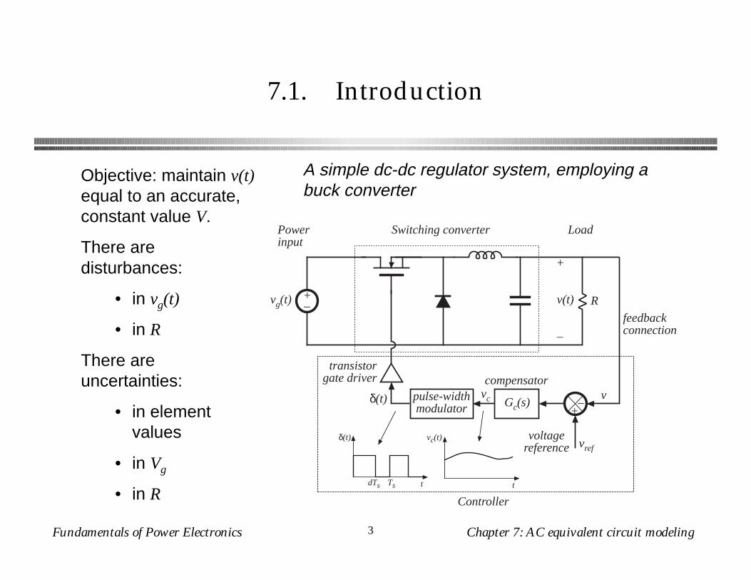
7.1. Introduction
+–
+
v(t)
–
vg(t)
Switching converterPowerinput
Load
–+
R
compensator
Gc(s)
vrefvoltage
reference
v
feedbackconnection
pulse-widthmodulator
vc
transistorgate driver
δ(t)
δ(t)
TsdTs t t
vc(t)
Controller
A simple dc-dc regulator system, employing a buck converter
Objective: maintain v(t) equal to an accurate, constant value V.
There are disturbances:
• in vg(t)
• in R
There are uncertainties:
• in element values
• in Vg
• in R
Fundamentals of Power Electronics Chapter 7: AC equivalent circuit modeling4
Applications of control in power electronics
Dc-dc converters
Regulate dc output voltage.
Control the duty cycle d(t) such that v(t) accurately follows a reference signal vref.
Dc-ac inverters
Regulate an ac output voltage.
Control the duty cycle d(t) such that v(t) accurately follows a reference signal vref (t).
Ac-dc rectifiers
Regulate the dc output voltage.
Regulate the ac input current waveform.
Control the duty cycle d(t) such that ig (t) accurately follows a reference signal iref (t), and v(t) accurately follows a reference signal vref.

Fundamentals of Power Electronics Chapter 7: AC equivalent circuit modeling5
Objective of Part II
Develop tools for modeling, analysis, and design of converter control systems
Need dynamic models of converters:
How do ac variations in vg(t), R, or d(t) affect the output voltage v(t)?
What are the small-signal transfer functions of the converter?
• Extend the steady-state converter models of Chapters 2 and 3, to include CCM converter dynamics (Chapter 7)
• Construct converter small-signal transfer functions (Chapter 8)
• Design converter control systems (Chapter 9)
• Model converters operating in DCM (Chapter 10)
• Current-programmed control of converters (Chapter 11)

Fundamentals of Power Electronics Chapter 7: AC equivalent circuit modeling6
Modeling
• Representation of physical behavior by mathematical means
• Model dominant behavior of system, ignore other insignificant phenomena
• Simplified model yields physical insight, allowing engineer to design system to operate in specified manner
• Approximations neglect small but complicating phenomena
• After basic insight has been gained, model can be refined (if it is judged worthwhile to expend the engineering effort to do so), to account for some of the previously neglected phenomena

Fundamentals of Power Electronics Chapter 7: AC equivalent circuit modeling7
Neglecting the switching ripple
t
t
gatedrive
actual waveform v(t)including ripple
averaged waveform <v(t)>Tswith ripple neglected
d(t) = D + Dm cos ωmt
Suppose the duty cycle is modulated sinusoidally:
where D and Dm are constants, | Dm | << D , and the modulation frequency ωm is much smaller than the converter switching frequency ωs = 2πfs.
The resulting variations in transistor gate drive signal and converter output voltage:

Fundamentals of Power Electronics Chapter 7: AC equivalent circuit modeling8
Output voltage spectrumwith sinusoidal modulation of duty cycle
spectrumof v(t)
ωm ωs ω
{modulationfrequency and its
harmonics {switchingfrequency and
sidebands {switchingharmonics
Contains frequency components at:• Modulation frequency and its
harmonics
• Switching frequency and its harmonics
• Sidebands of switching frequency
With small switching ripple, high-frequency components (switching harmonics and sidebands) are small.
If ripple is neglected, then only low-frequency components (modulation frequency and harmonics) remain.

Fundamentals of Power Electronics Chapter 7: AC equivalent circuit modeling9
Objective of ac converter modeling
• Predict how low-frequency variations in duty cycle induce low-frequency variations in the converter voltages and currents
• Ignore the switching ripple
• Ignore complicated switching harmonics and sidebands
Approach:
• Remove switching harmonics by averaging all waveforms over one switching period

Fundamentals of Power Electronics Chapter 7: AC equivalent circuit modeling10
Averaging to remove switching ripple
Ld iL(t) Ts
dt= vL(t) Ts
Cd vC(t)
Ts
dt= iC(t)
Ts
xL(t) Ts= 1
Tsx(τ) dτ
t
t + Ts
where
Average over one switching period to remove switching ripple:
Note that, in steady-state,
vL(t) Ts= 0
iC(t)Ts
= 0
by inductor volt-second balance and capacitor charge balance.

Fundamentals of Power Electronics Chapter 7: AC equivalent circuit modeling11
Nonlinear averaged equations
Ld iL(t) Ts
dt= vL(t) Ts
Cd vC(t)
Ts
dt= iC(t)
Ts
The averaged voltages and currents are, in general, nonlinear functions of the converter duty cycle, voltages, and currents. Hence, the averaged equations
constitute a system of nonlinear differential equations.
Hence, must linearize by constructing a small-signal converter model.

Fundamentals of Power Electronics Chapter 7: AC equivalent circuit modeling12
Small-signal modeling of the BJT
iBβFiB
βRiBB
C
E
iB
B
C
E
βFiB
rE
Nonlinear Ebers-Moll model Linearized small-signal model, active region

Fundamentals of Power Electronics Chapter 7: AC equivalent circuit modeling13
Buck-boost converter:nonlinear static control-to-output characteristic
D
V
–Vg
0.5 100
actualnonlinear
characteristic
linearizedfunction
quiescentoperatingpoint Example: linearization
at the quiescent operating point
D = 0.5

Fundamentals of Power Electronics Chapter 7: AC equivalent circuit modeling14
Result of averaged small-signal ac modeling
+– I d(t)vg(t)
+–
LVg – V d(t)
+
v(t)
–
RCI d(t)
1 : D D' : 1
Small-signal ac equivalent circuit model
buck-boost example

Fundamentals of Power Electronics Chapter 7: AC equivalent circuit modeling15
7.2. The basic ac modeling approach
+–
LC R
+
v(t)
–
1 2
i(t)vg(t)
Buck-boost converter example

Fundamentals of Power Electronics Chapter 7: AC equivalent circuit modeling16
Switch in position 1
vL(t) = Ldi(t)dt
= vg(t)
iC(t) = Cdv(t)
dt= –
v(t)R
iC(t) = Cdv(t)
dt≈ –
v(t)Ts
R
vL(t) = Ldi(t)dt
≈ vg(t) Ts
Inductor voltage and capacitor current are:
Small ripple approximation: replace waveforms with their low-frequency averaged values:
+– L C R
+
v(t)
–
i(t)
vg(t)

Fundamentals of Power Electronics Chapter 7: AC equivalent circuit modeling17
Switch in position 2
Inductor voltage and capacitor current are:
Small ripple approximation: replace waveforms with their low-frequency averaged values:
+– L C R
+
v(t)
–
i(t)
vg(t)vL(t) = L
di(t)dt
= v(t)
iC(t) = Cdv(t)
dt= – i(t) –
v(t)R
vL(t) = Ldi(t)dt
≈ v(t)Ts
iC(t) = Cdv(t)
dt≈ – i(t)
Ts–
v(t)Ts
R

Fundamentals of Power Electronics Chapter 7: AC equivalent circuit modeling18
7.2.1 Averaging the inductor waveforms
Inductor voltage waveform
t
vL(t)
dTs Ts0
v(t)Ts
vg(t) Ts
vL(t)Ts
= d vg(t) Ts+ d' v(t)
Ts
Low-frequency average is found by evaluation of
xL(t) Ts= 1
Tsx(τ)dτ
t
t + Ts
Average the inductor voltage in this manner:
vL(t) Ts= 1
TsvL(τ)dτ
t
t + Ts
≈ d(t) vg(t) Ts+ d'(t) v(t)
Ts
Insert into Eq. (7.2):
Ld i(t)
Ts
dt= d(t) vg(t) Ts
+ d'(t) v(t)Ts
This equation describes how the low-frequency components of the inductor waveforms evolve in time.

Fundamentals of Power Electronics Chapter 7: AC equivalent circuit modeling19
7.2.2 Discussion of the averaging approximation
t
vL(t)
dTs Ts0
v(t)Ts
vg(t) Ts
vL(t)Ts
= d vg(t) Ts+ d' v(t)
Ts
vg Ts
L
v Ts
L
t
i(t)
i(0)
i(dTs)
i(Ts)
dTs Ts0
Inductor voltage and current waveforms
Use of the average inductor voltage allows us to determine the net change in inductor current over one switching period, while neglecting the switching ripple.
In steady-state, the average inductor voltage is zero (volt-second balance), and hence the inductor current waveform is periodic: i(t + Ts) = i(t). There is no net change in inductor current over one switching period.
During transients or ac variations, the average inductor voltage is not zero in general, and this leads to net variations in inductor current.

Fundamentals of Power Electronics Chapter 7: AC equivalent circuit modeling20
Net change in inductor current is correctly predicted by the average inductor voltage
Ldi(t)dt
= vL(t)Inductor equation:
Divide by L and integrate over one switching period:
dit
t + Ts
= 1L vL(τ)dτ
t
t + Ts
Left-hand side is the change in inductor current. Right-hand side can be related to average inductor voltage by multiplying and dividing by Ts as follows:
i(t + Ts) – i(t) = 1L
Ts vL(t) Ts
So the net change in inductor current over one switching period is exactly equal to the period Ts multiplied by the average slope ⟨ vL ⟩Ts /L.

Fundamentals of Power Electronics Chapter 7: AC equivalent circuit modeling21
Average inductor voltage correctly predicts average slope of iL(t)
The net change in inductor current over one switching period is exactly equal to the period Ts multiplied by the average slope ⟨ vL ⟩Ts /L.
vg(t)L
v(t)L
t
i(t)
i(0) i(Ts)
dTs Ts0
d vg(t) Ts+ d' v(t)
Ts
L
i(t)Ts
Actual waveform,including ripple
Averaged waveform

Fundamentals of Power Electronics Chapter 7: AC equivalent circuit modeling22
d i(t)Ts
dt
We have
i(t + Ts) – i(t) = 1L
Ts vL(t) Ts
Rearrange:
Li(t + Ts) – i(t)
Ts= vL(t) Ts
Define the derivative of ⟨ i ⟩Ts as (Euler formula):
d i(t)Ts
dt=
i(t + Ts) – i(t)Ts
Hence,
Ld i(t)
Ts
dt= vL(t) Ts

Fundamentals of Power Electronics Chapter 7: AC equivalent circuit modeling23
Computing how the inductor current changes over one switching period
vg Ts
L
v Ts
L
t
i(t)
i(0)
i(dTs)
i(Ts)
dTs Ts0
With switch in position 1:
i(dTs) = i(0) + dTs
vg(t) Ts
L
(final value) = (initial value) + (length of interval) (average slope)
i(Ts) = i(dTs) + d'Ts
v(t)Ts
L
(final value) = (initial value) + (length of interval) (average slope)
With switch in position 2:
Let’s compute the actual inductor current waveform, using the linear ripple approximation.

Fundamentals of Power Electronics Chapter 7: AC equivalent circuit modeling24
Net change in inductor current over one switching period
Eliminate i(dTs), to express i(Ts) directly as a function of i(0): i(Ts) = i(0) +
Ts
L d(t) vg(t) Ts+ d'(t) v(t)
Ts
vL(t) Ts
vg(t)L
v(t)L
t
i(t)
i(0) i(Ts)
dTs Ts0
d vg(t) Ts+ d' v(t)
Ts
L
i(t)Ts
Actual waveform,including ripple
Averaged waveformThe intermediate step of computing i(dTs) is eliminated.
The final value i(Ts) is equal to the initial value i(0), plus the switching period Ts multiplied by the average slope ⟨ vL ⟩Ts /L.
Fundamentals of Power Electronics Chapter 7: AC equivalent circuit modeling25
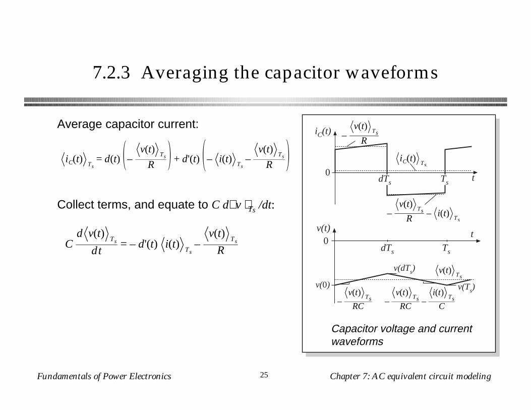
7.2.3 Averaging the capacitor waveforms
t
iC(t)
dTs Ts0
–v(t)
Ts
R– i(t)
Ts
–v(t)
Ts
R
iC(t)Ts
Capacitor voltage and current waveforms
tv(t)
dTs Ts
0
v(0)
v(dTs)
v(Ts)
v(t)Ts
–v(t)
Ts
RC –v(t)
Ts
RC –i(t)
Ts
C
Average capacitor current:
iC(t)Ts
= d(t) –v(t)
Ts
R+ d'(t) – i(t)
Ts–
v(t)Ts
R
Collect terms, and equate to C d⟨ v ⟩Ts /dt:
Cd v(t)
Ts
dt= – d'(t) i(t)
Ts–
v(t)Ts
R

Fundamentals of Power Electronics Chapter 7: AC equivalent circuit modeling26
7.2.4 The average input current
t
ig(t)
dTs Ts
00
i(t)Ts
ig(t) Ts
0
Converter input current waveform
We found in Chapter 3 that it was sometimes necessary to write an equation for the average converter input current, to derive a complete dc equivalent circuit model. It is likewise necessary to do this for the ac model.
Buck-boost input current waveform is
ig(t) =i(t)
Tsduring subinterval 1
0 during subinterval 2
Average value:
ig(t) Ts= d(t) i(t)
Ts
Fundamentals of Power Electronics Chapter 7: AC equivalent circuit modeling27
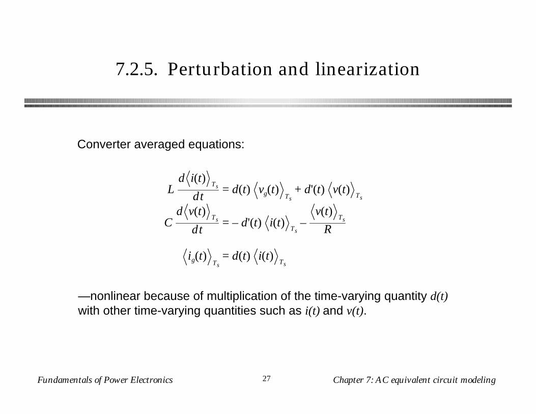
7.2.5. Perturbation and linearization
Ld i(t)
Ts
dt= d(t) vg(t) Ts
+ d'(t) v(t)Ts
Cd v(t)
Ts
dt= – d'(t) i(t)
Ts–
v(t)Ts
R
ig(t) Ts= d(t) i(t)
Ts
Converter averaged equations:
—nonlinear because of multiplication of the time-varying quantity d(t) with other time-varying quantities such as i(t) and v(t).

Fundamentals of Power Electronics Chapter 7: AC equivalent circuit modeling28
Construct small-signal model:Linearize about quiescent operating point
If the converter is driven with some steady-state, or quiescent, inputs
d(t) = D
vg(t) Ts= Vg
then, from the analysis of Chapter 2, after transients have subsided the inductor current, capacitor voltage, and input current
i(t)Ts
, v(t)Ts
, ig(t) Ts
reach the quiescent values I, V, and Ig, given by the steady-state analysis as
V = – DD'
Vg
I = – VD' R
Ig = D I

Fundamentals of Power Electronics Chapter 7: AC equivalent circuit modeling29
Perturbation
So let us assume that the input voltage and duty cycle are equal to some given (dc) quiescent values, plus superimposed small ac variations:
vg(t) Ts= Vg + vg(t)
d(t) = D + d(t)
In response, and after any transients have subsided, the converter dependent voltages and currents will be equal to the corresponding quiescent values, plus small ac variations:
i(t)Ts
= I + i(t)
v(t)Ts
= V + v(t)
ig(t) Ts= Ig + ig(t)

Fundamentals of Power Electronics Chapter 7: AC equivalent circuit modeling30
The small-signal assumption
vg(t) << Vg
d(t) << D
i(t) << I
v(t) << V
ig(t) << Ig
If the ac variations are much smaller in magnitude than the respective quiescent values,
then the nonlinear converter equations can be linearized.
Fundamentals of Power Electronics Chapter 7: AC equivalent circuit modeling31
Perturbation of inductor equation
Insert the perturbed expressions into the inductor differential equation:
Ld I + i(t)
dt= D + d(t) Vg + vg(t) + D' – d(t) V + v(t)
note that d’(t) is given by
d'(t) = 1 – d(t) = 1 – D + d(t) = D' – d(t) with D’ = 1 – D
Multiply out and collect terms:
L dIdt➚
0
+d i(t)
dt= DVg+ D'V + Dvg(t) + D'v(t) + Vg – V d(t) + d(t) vg(t) – v(t)
Dc terms 1 st order ac terms 2nd order ac terms(linear) (nonlinear)
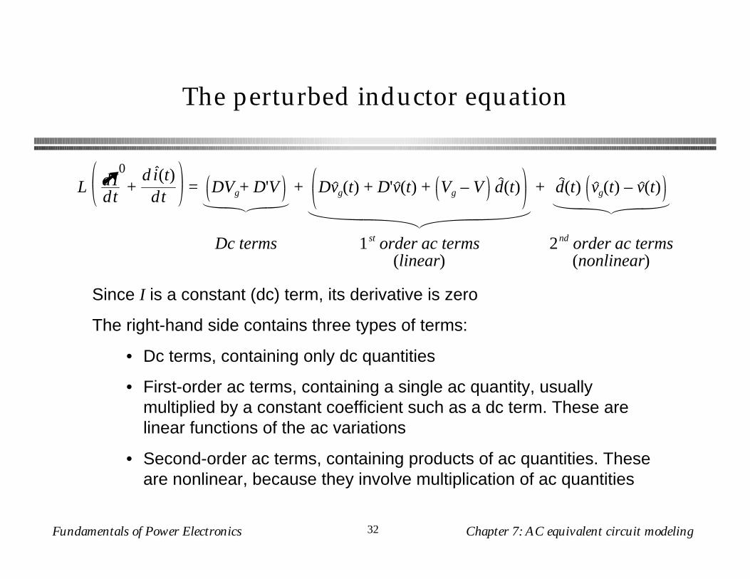
Fundamentals of Power Electronics Chapter 7: AC equivalent circuit modeling32
The perturbed inductor equation
L dIdt➚
0
+d i(t)
dt= DVg+ D'V + Dvg(t) + D'v(t) + Vg – V d(t) + d(t) vg(t) – v(t)
Dc terms 1 st order ac terms 2nd order ac terms(linear) (nonlinear)
Since I is a constant (dc) term, its derivative is zero
The right-hand side contains three types of terms:
• Dc terms, containing only dc quantities
• First-order ac terms, containing a single ac quantity, usually multiplied by a constant coefficient such as a dc term. These are linear functions of the ac variations
• Second-order ac terms, containing products of ac quantities. These are nonlinear, because they involve multiplication of ac quantities

Fundamentals of Power Electronics Chapter 7: AC equivalent circuit modeling33
Neglect of second-order terms
L dIdt➚
0
+d i(t)
dt= DVg+ D'V + Dvg(t) + D'v(t) + Vg – V d(t) + d(t) vg(t) – v(t)
Dc terms 1 st order ac terms 2nd order ac terms(linear) (nonlinear)
vg(t) << Vg
d(t) << D
i(t) << I
v(t) << V
ig(t) << Ig
Provided then the second-order ac terms are much smaller than the first-order terms. For example,
d(t) vg(t) << D vg(t) d(t) << Dwhen
So neglect second-order terms.Also, dc terms on each side of equation
are equal.

Fundamentals of Power Electronics Chapter 7: AC equivalent circuit modeling34
Linearized inductor equation
Upon discarding second-order terms, and removing dc terms (which add to zero), we are left with
Ld i(t)
dt= Dvg(t) + D'v(t) + Vg – V d(t)
This is the desired result: a linearized equation which describes small-signal ac variations.
Note that the quiescent values D, D’, V, Vg, are treated as given constants in the equation.

Fundamentals of Power Electronics Chapter 7: AC equivalent circuit modeling35
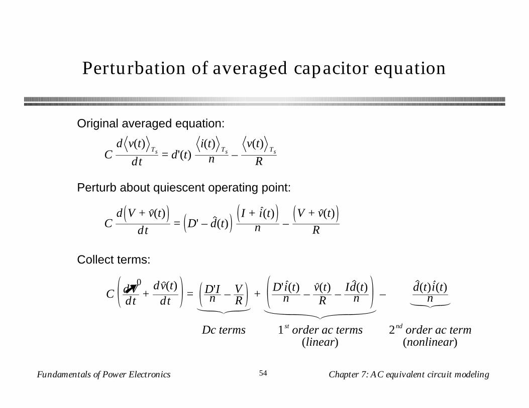
Capacitor equation
Perturbation leads to
C dVdt➚
0+
dv(t)dt
= – D'I – VR + – D'i(t) –
v(t)R + Id(t) + d(t)i(t)
Dc terms 1 st order ac terms 2nd order ac term(linear) (nonlinear)
Neglect second-order terms. Dc terms on both sides of equation are equal. The following terms remain:
Cdv(t)
dt= – D'i(t) –
v(t)R + Id(t)
This is the desired small-signal linearized capacitor equation.
Cd V + v(t)
dt= – D' – d(t) I + i(t) –
V + v(t)
R
Collect terms:

Fundamentals of Power Electronics Chapter 7: AC equivalent circuit modeling36
Average input current
Perturbation leads to
Ig + ig(t) = D + d(t) I + i(t)
Collect terms:
Ig + ig(t) = DI + Di(t) + Id(t) + d(t)i(t)
Dc term 1 st order ac term Dc term 1 st order ac terms 2nd order ac term(linear) (nonlinear)
Neglect second-order terms. Dc terms on both sides of equation are equal. The following first-order terms remain:
ig(t) = Di(t) + Id(t)
This is the linearized small-signal equation which described the converter input port.

Fundamentals of Power Electronics Chapter 7: AC equivalent circuit modeling37
7.2.6. Construction of small-signalequivalent circuit model
The linearized small-signal converter equations:
Ld i(t)
dt= Dvg(t) + D'v(t) + Vg – V d(t)
Cdv(t)
dt= – D'i(t) –
v(t)R + Id(t)
ig(t) = Di(t) + Id(t)
Reconstruct equivalent circuit corresponding to these equations, in manner similar to the process used in Chapter 3.
Fundamentals of Power Electronics Chapter 7: AC equivalent circuit modeling38
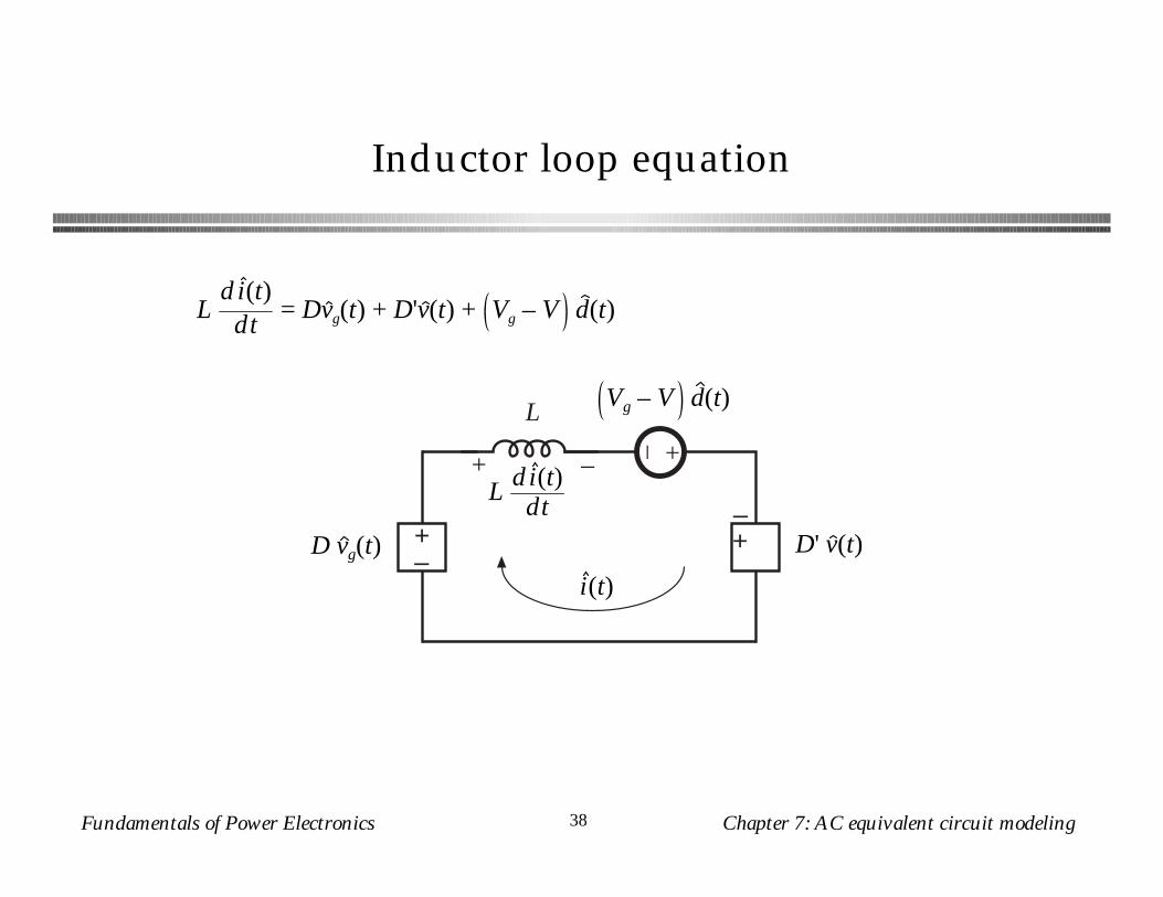
Inductor loop equation
Ld i(t)
dt= Dvg(t) + D'v(t) + Vg – V d(t)
+–
+–
+–
L
D' v(t)
Vg – V d(t)
Ld i(t)
dt
D vg(t)
i(t)
+ –
Fundamentals of Power Electronics Chapter 7: AC equivalent circuit modeling39
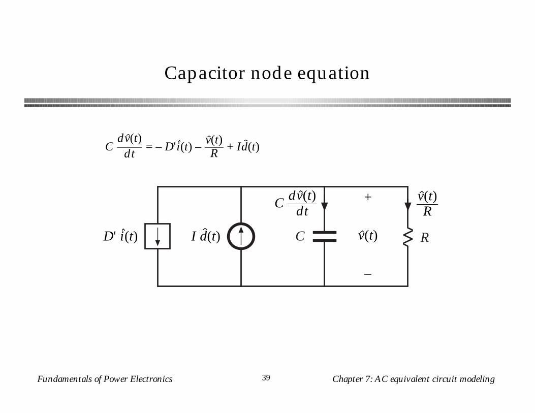
Capacitor node equation
+
v(t)
–
RC
Cdv(t)
dt
D' i(t) I d(t)
v(t)R
Cdv(t)
dt= – D'i(t) –
v(t)R + Id(t)

Fundamentals of Power Electronics Chapter 7: AC equivalent circuit modeling40
Input port node equation
ig(t) = Di(t) + Id(t)
+– D i(t)I d(t)
i g(t)
vg(t)

Fundamentals of Power Electronics Chapter 7: AC equivalent circuit modeling41
Complete equivalent circuit
Collect the three circuits:
+– D i(t)I d(t)vg(t) +
–
+–
+–
L
D' v(t)
Vg – V d(t)
D vg(t)
i(t)
+
v(t)
–
RCD' i(t) I d(t)
Replace dependent sources with ideal dc transformers:
+– I d(t)vg(t)
+–L
Vg – V d(t)
+
v(t)
–
RCI d(t)
1 : D D' : 1
Small-signal ac equivalent circuit model of the buck-boost converter
Fundamentals of Power Electronics Chapter 7: AC equivalent circuit modeling42
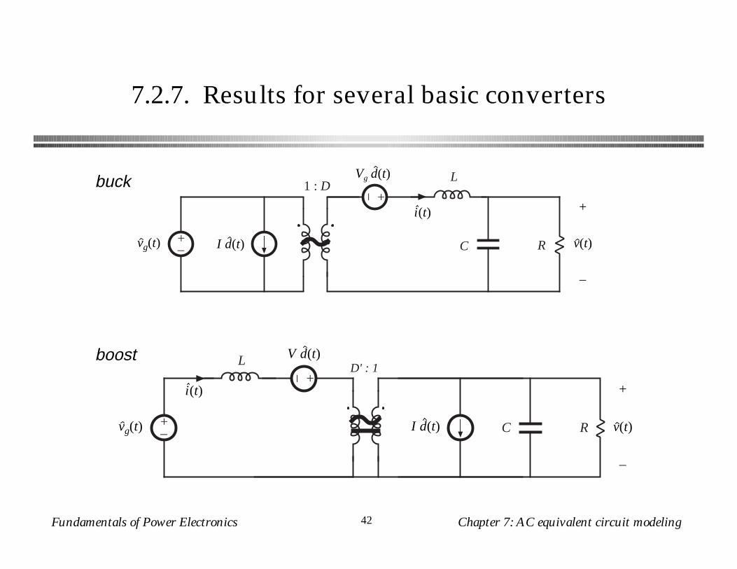
7.2.7. Results for several basic converters
+– I d(t)vg(t)
+–
LVg d(t)
+
v(t)
–
RC
1 : D
i(t)
+–
L
C Rvg(t)
i(t) +
v(t)
–
+–
V d(t)
I d(t)
D' : 1
buck
boost
Fundamentals of Power Electronics Chapter 7: AC equivalent circuit modeling43
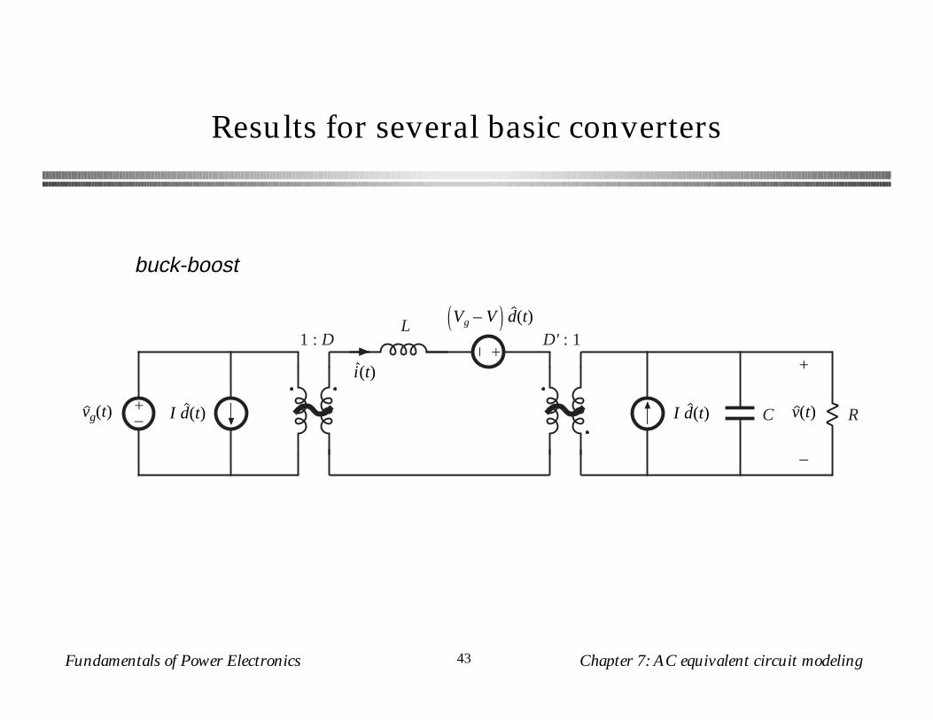
Results for several basic converters
+– I d(t)vg(t)
+–
LVg – V d(t)
+
v(t)
–
RCI d(t)
1 : D D' : 1
i(t)
buck-boost
Fundamentals of Power Electronics Chapter 7: AC equivalent circuit modeling44
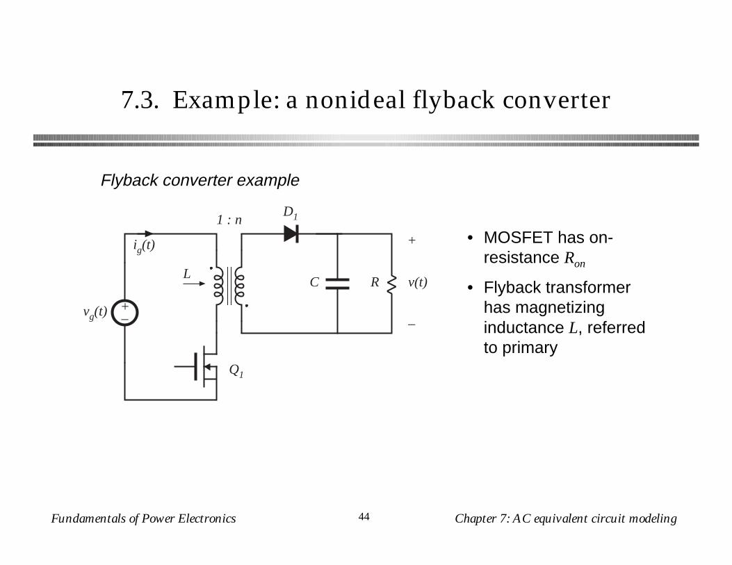
7.3. Example: a nonideal flyback converter
+–
D1
Q1
C R
+
v(t)
–
1 : n
vg(t)
ig(t)
L
Flyback converter example
• MOSFET has on-resistance Ron
• Flyback transformer has magnetizing inductance L, referred to primary
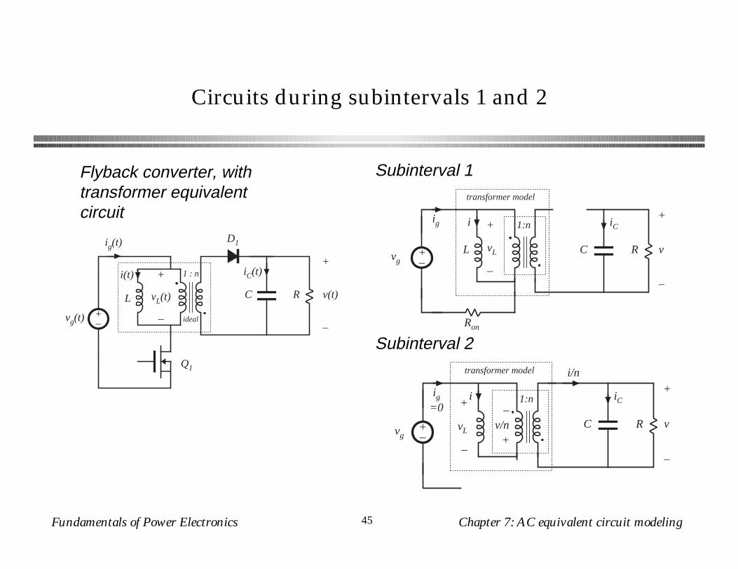
Fundamentals of Power Electronics Chapter 7: AC equivalent circuit modeling45
Circuits during subintervals 1 and 2
+–
D1
Q1
C R
+
v(t)
–vg(t)
ig(t)
L
i(t) iC(t)+
vL(t)
–
1 : n
ideal
+–
L
+
v
–
vg
1:n
C
transformer model
iig
R
iC+
vL
–
Ron
+–
+
v
–
vg
1:n
C
transformer model
i
R
iC
i/n
–v/n
+
+
vL
–
ig=0
Flyback converter, with transformer equivalent circuit
Subinterval 1
Subinterval 2

Fundamentals of Power Electronics Chapter 7: AC equivalent circuit modeling46
Subinterval 1
+–
L
+
v
–
vg
1:n
C
transformer model
iig
R
iC+
vL
–
Ron
vL(t) = vg(t) – i(t) Ron
iC(t) = –v(t)R
ig(t) = i(t)
Circuit equations:
Small ripple approximation:
vL(t) = vg(t) Ts– i(t)
TsRon
iC(t) = –v(t)
Ts
Rig(t) = i(t)
Ts
MOSFET conducts, diode is reverse-biased
Fundamentals of Power Electronics Chapter 7: AC equivalent circuit modeling47
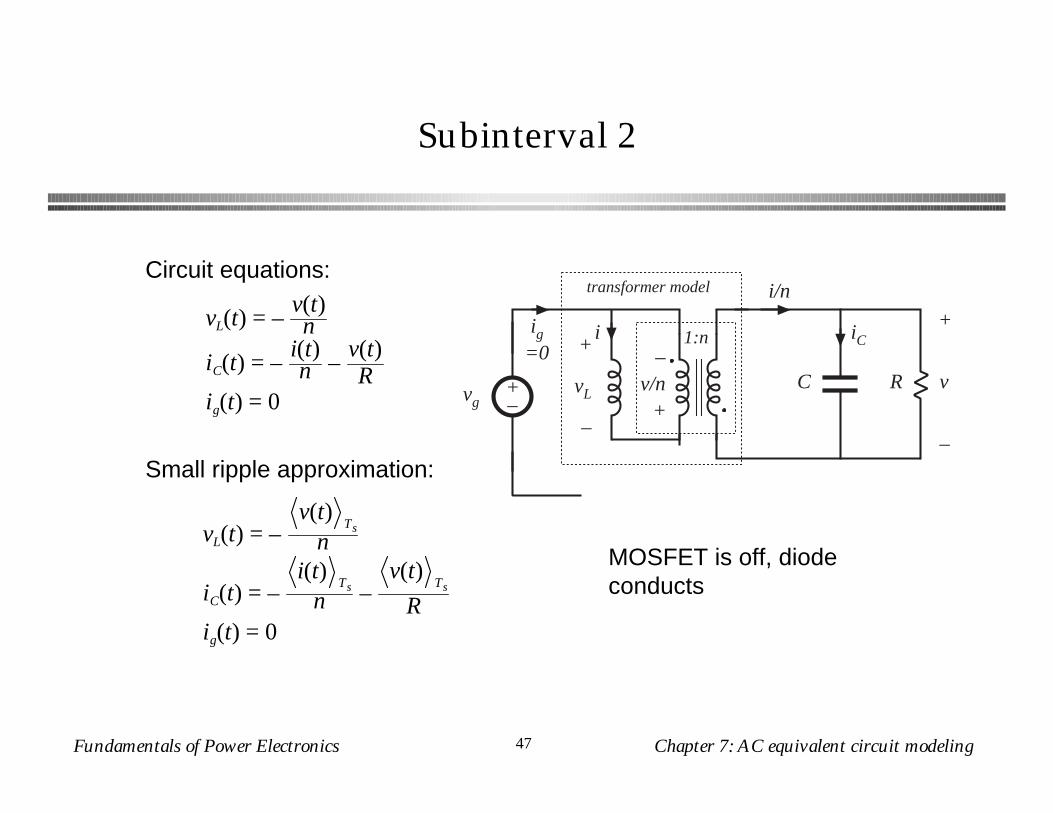
Subinterval 2
Circuit equations:
Small ripple approximation:
MOSFET is off, diode conducts
vL(t) = –v(t)n
iC(t) = –i(t)n –
v(t)R
ig(t) = 0
vL(t) = –v(t)
Ts
n
iC(t) = –i(t)
Ts
n –v(t)
Ts
Rig(t) = 0
+–
+
v
–
vg
1:n
C
transformer model
i
R
iC
i/n
–v/n
+
+
vL
–
ig=0
Fundamentals of Power Electronics Chapter 7: AC equivalent circuit modeling48
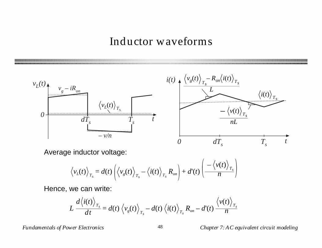
Inductor waveforms
t
vL(t)
dTs Ts0
vg – iRon
– v/n
vL(t)Ts
t
i(t)
dTs Ts0
i(t)Ts
– v(t)Ts
nL
vg(t) Ts– Ron i(t)
Ts
L
vL(t) Ts= d(t) vg(t) Ts
– i(t)Ts
Ron + d'(t)– v(t)
Ts
n
Ld i(t)
Ts
dt= d(t) vg(t) Ts
– d(t) i(t)Ts
Ron – d'(t)v(t)
Ts
n
Average inductor voltage:
Hence, we can write:
Fundamentals of Power Electronics Chapter 7: AC equivalent circuit modeling49
Capacitor waveforms
Average capacitor current:
Hence, we can write:
t
iC(t)
dTs Ts0
– v/R
iC(t)Ts
in – v
R
t
v(t)
dTs Ts0
v(t)Ts
–v(t)
Ts
RC
i(t)Ts
nC –v(t)
Ts
RC
iC(t)Ts
= d(t)– v(t)
Ts
R + d'(t)i(t)
Ts
n –v(t)
Ts
R
Cd v(t)
Ts
dt= d'(t)
i(t)Ts
n –v(t)
Ts
R

Fundamentals of Power Electronics Chapter 7: AC equivalent circuit modeling50
Input current waveform
Average input current:
t
ig(t)
dTs Ts
00
i(t)Ts
ig(t) Ts
0
ig(t) Ts= d(t) i(t)
Ts

Fundamentals of Power Electronics Chapter 7: AC equivalent circuit modeling51
The averaged converter equations
Ld i(t)
Ts
dt= d(t) vg(t) Ts
– d(t) i(t)Ts
Ron – d'(t)v(t)
Ts
n
Cd v(t)
Ts
dt= d'(t)
i(t)Ts
n –v(t)
Ts
R
ig(t) Ts= d(t) i(t)
Ts
— a system of nonlinear differential equations
Next step: perturbation and linearization. Let
vg(t) Ts= Vg + vg(t)
d(t) = D + d(t)
i(t)Ts
= I + i(t)
v(t)Ts
= V + v(t)
ig(t) Ts= Ig + ig(t)

Fundamentals of Power Electronics Chapter 7: AC equivalent circuit modeling52
L dIdt➚
0
+d i(t)
dt= DVg– D'Vn – DRonI + Dvg(t) – D'
v(t)n + Vg + V
n – IRon d(t) – DRoni(t)
Dc terms 1 st order ac terms (linear)
+ d(t)vg(t) + d(t)v(t)n – d(t)i(t)Ron
2nd order ac terms (nonlinear)
Perturbation of the averaged inductor equation
Ld i(t)
Ts
dt= d(t) vg(t) Ts
– d(t) i(t)Ts
Ron – d'(t)v(t)
Ts
n
Ld I + i(t)
dt= D + d(t) Vg + vg(t) – D' – d(t)
V + v(t)n – D + d(t) I + i(t) Ron

Fundamentals of Power Electronics Chapter 7: AC equivalent circuit modeling53
Linearization of averaged inductor equation
Dc terms:
Second-order terms are small when the small-signal assumption is satisfied. The remaining first-order terms are:
0 = DVg– D'Vn – DRonI
Ld i(t)
dt= Dvg(t) – D'
v(t)n + Vg + V
n – IRon d(t) – DRoni(t)
This is the desired linearized inductor equation.
Fundamentals of Power Electronics Chapter 7: AC equivalent circuit modeling54
Perturbation of averaged capacitor equation
Cd v(t)
Ts
dt= d'(t)
i(t)Ts
n –v(t)
Ts
R
Cd V + v(t)
dt= D' – d(t)
I + i(t)n –
V + v(t)
R
C dVdt➚
0+
dv(t)dt
= D'In – V
R +D'i(t)
n –v(t)R –
Id(t)n –
d(t)i(t)n
Dc terms 1 st order ac terms 2nd order ac term(linear) (nonlinear)
Original averaged equation:
Perturb about quiescent operating point:
Collect terms:

Fundamentals of Power Electronics Chapter 7: AC equivalent circuit modeling55
Linearization of averaged capacitor equation
0 = D'In – V
R
Cdv(t)
dt=
D'i(t)n –
v(t)R –
Id(t)n
Dc terms:
Second-order terms are small when the small-signal assumption is satisfied. The remaining first-order terms are:
This is the desired linearized capacitor equation.

Fundamentals of Power Electronics Chapter 7: AC equivalent circuit modeling56
Perturbation of averaged input current equation
Original averaged equation:
Perturb about quiescent operating point:
Collect terms:
ig(t) Ts= d(t) i(t)
Ts
Ig + ig(t) = D + d(t) I + i(t)
Ig + ig(t) = DI + Di(t) + Id(t) + d(t)i(t)
Dc term 1 st order ac term Dc term 1 st order ac terms 2nd order ac term(linear) (nonlinear)

Fundamentals of Power Electronics Chapter 7: AC equivalent circuit modeling57
Linearization of averaged input current equation
Dc terms:
Second-order terms are small when the small-signal assumption is satisfied. The remaining first-order terms are:
This is the desired linearized input current equation.
Ig = DI
ig(t) = Di(t) + Id(t)
Fundamentals of Power Electronics Chapter 7: AC equivalent circuit modeling58
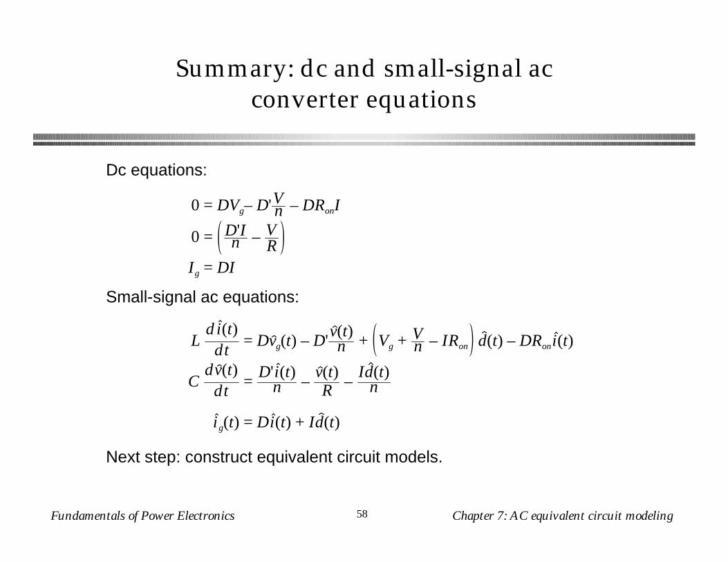
Summary: dc and small-signal acconverter equations
0 = DVg– D'Vn – DRonI
0 = D'In – V
RIg = DI
Ld i(t)
dt= Dvg(t) – D'
v(t)n + Vg + V
n – IRon d(t) – DRoni(t)
Cdv(t)
dt=
D'i(t)n –
v(t)R –
Id(t)n
ig(t) = Di(t) + Id(t)
Dc equations:
Small-signal ac equations:
Next step: construct equivalent circuit models.

Fundamentals of Power Electronics Chapter 7: AC equivalent circuit modeling59
Small-signal ac equivalent circuit:inductor loop
Ld i(t)
dt= Dvg(t) – D'
v(t)n + Vg + V
n – IRon d(t) – DRoni(t)
+–
+–
+–
L
D' v(t)n
d(t) Vg – IRon + Vn
Ld i(t)
dt
D vg(t)i(t)
+ –
DRon
Fundamentals of Power Electronics Chapter 7: AC equivalent circuit modeling60
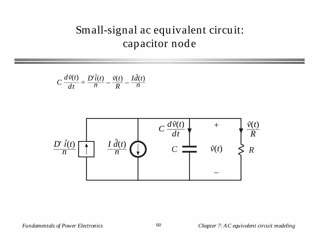
Small-signal ac equivalent circuit:capacitor node
Cdv(t)
dt=
D'i(t)n –
v(t)R –
Id(t)n
+
v(t)
–
RC
Cdv(t)
dtD' i(t)
nI d(t)
n
v(t)R
Fundamentals of Power Electronics Chapter 7: AC equivalent circuit modeling61
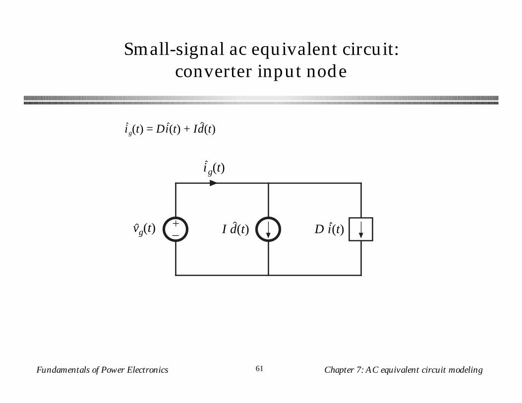
Small-signal ac equivalent circuit:converter input node
ig(t) = Di(t) + Id(t)
+– D i(t)I d(t)
i g(t)
vg(t)
Fundamentals of Power Electronics Chapter 7: AC equivalent circuit modeling62
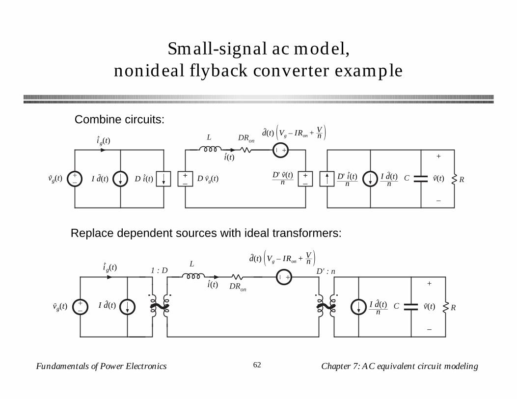
Small-signal ac model,nonideal flyback converter example
Combine circuits:
Replace dependent sources with ideal transformers:
+– D i(t)I d(t)
i g(t)
vg(t) +–
+–
+–
L
D' v(t)n
d(t) Vg – IRon + Vn
D vg(t)
i(t)
DRon
+
v(t)
–
RCD' i(t)n
I d(t)n
+–
I d(t)
i g(t)
vg(t)
Ld(t) Vg – IRon + V
n
i(t) DRon+
v(t)
–
RCI d(t)n
1 : D +– D' : n

Fundamentals of Power Electronics Chapter 7: AC equivalent circuit modeling63
7.4. State Space Averaging
• A formal method for deriving the small-signal ac equations of a switching converter
• Equivalent to the modeling method of the previous sections
• Uses the state-space matrix description of linear circuits
• Often cited in the literature
• A general approach: if the state equations of the converter can be written for each subinterval, then the small-signal averaged model can always be derived
• Computer programs exist which utilize the state-space averaging method

Fundamentals of Power Electronics Chapter 7: AC equivalent circuit modeling64
7.4.1. The state equations of a network
• A canonical form for writing the differential equations of a system
• If the system is linear, then the derivatives of the state variables are expressed as linear combinations of the system independent inputs and state variables themselves
• The physical state variables of a system are usually associated with the storage of energy
• For a typical converter circuit, the physical state variables are the inductor currents and capacitor voltages
• Other typical physical state variables: position and velocity of a motor shaft
• At a given point in time, the values of the state variables depend on the previous history of the system, rather than the present values of the system inputs
• To solve the differential equations of a system, the initial values of the state variables must be specified

Fundamentals of Power Electronics Chapter 7: AC equivalent circuit modeling65
State equations of a linear system, in matrix form
x(t) =x1(t)x2(t) ,
dx(t)dt
=
dx1(t)dt
dx2(t)dt
A canonical matrix form:
State vector x(t) contains inductor currents, capacitor voltages, etc.:
Input vector u(t) contains independent sources such as vg(t)
Output vector y(t) contains other dependent quantities to be computed, such as ig(t)
Matrix K contains values of capacitance, inductance, and mutual inductance, so that K dx/dt is a vector containing capacitor currents and inductor winding voltages. These quantities are expressed as linear combinations of the independent inputs and state variables. The matrices A, B, C, and E contain the constants of proportionality.
K dx(t)dt
= A x(t) + B u(t)
y(t) = C x(t) + E u(t)
Fundamentals of Power Electronics Chapter 7: AC equivalent circuit modeling66
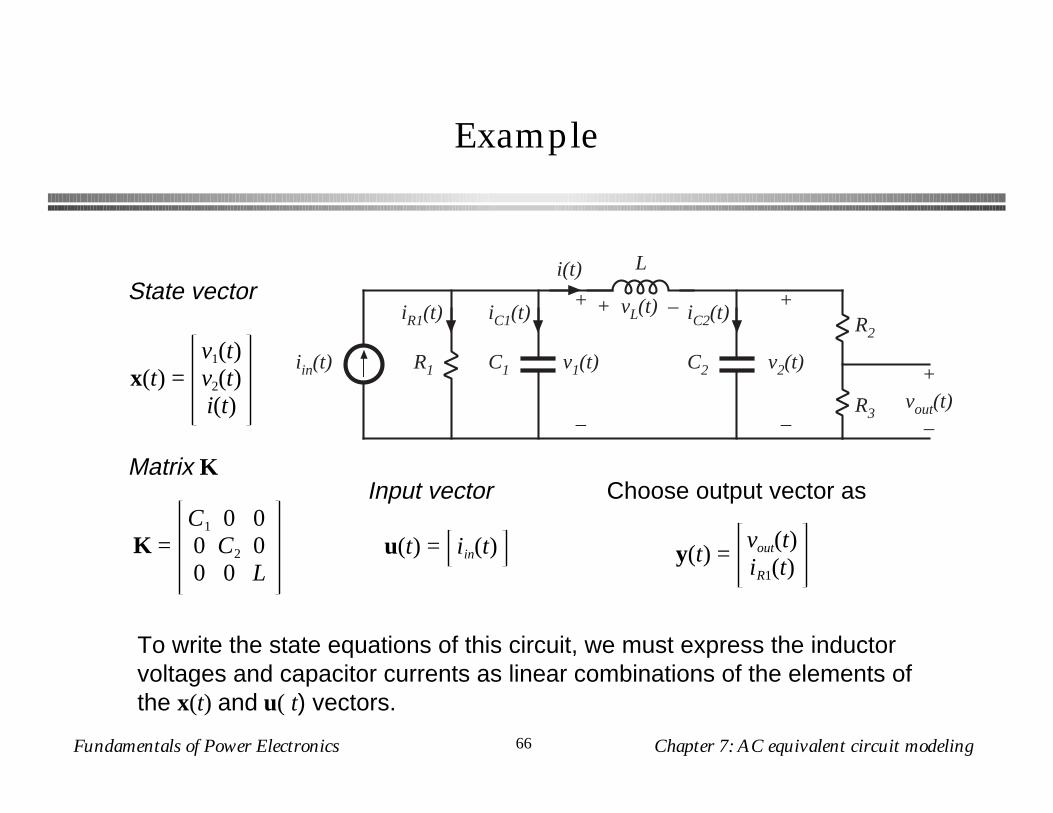
Example
iin(t) R1 C1
L
C2
R3
R2
+
v1(t)
–
+
v2(t)
–
+vout(t)
–
+ vL(t) –iR1(t) iC1(t) iC2(t)
i(t)State vector
x(t) =v1(t)v2(t)i(t)
Matrix K
K =C1 0 00 C2 00 0 L
Input vector
u(t) = iin(t)
Choose output vector as
y(t) =vout(t)iR1(t)
To write the state equations of this circuit, we must express the inductor voltages and capacitor currents as linear combinations of the elements of the x(t) and u( t) vectors.

Fundamentals of Power Electronics Chapter 7: AC equivalent circuit modeling67
Circuit equations
iin(t) R1 C1
L
C2
R3
R2
+
v1(t)
–
+
v2(t)
–
+vout(t)
–
+ vL(t) –iR1(t) iC1(t) iC2(t)
i(t)
iC1(t) = C1
dv1(t)dt
= iin(t) –v1(t)
R – i(t)
iC2(t) = C2
dv2(t)dt
= i(t) –v2(t)
R2 + R3
vL(t) = Ldi(t)dt
= v1(t) – v2(t)
Find iC1 via node equation:
Find iC2 via node equation:
Find vL via loop equation:

Fundamentals of Power Electronics Chapter 7: AC equivalent circuit modeling68
Equations in matrix form
C1 0 00 C2 00 0 L
dv1(t)dt
dv2(t)dt
di(t)dt
=
– 1R1
0 – 1
0 – 1R2 + R3
1
1 – 1 0
v1(t)v2(t)i(t)
+100
iin(t)
K dx(t)dt
= A x(t) + B u(t)
iC1(t) = C1
dv1(t)dt
= iin(t) –v1(t)
R – i(t)
iC2(t) = C2
dv2(t)dt
= i(t) –v2(t)
R2 + R3
vL(t) = Ldi(t)dt
= v1(t) – v2(t)
The same equations:
Express in matrix form:

Fundamentals of Power Electronics Chapter 7: AC equivalent circuit modeling69
Output (dependent signal) equations
iin(t) R1 C1
L
C2
R3
R2
+
v1(t)
–
+
v2(t)
–
+vout(t)
–
+ vL(t) –iR1(t) iC1(t) iC2(t)
i(t)
Express elements of the vector y as linear combinations of elements of x and u:
y(t) =vout(t)iR1(t)
vout(t) = v2(t)R3
R2 + R3
iR1(t) =v1(t)
R1

Fundamentals of Power Electronics Chapter 7: AC equivalent circuit modeling70
Express in matrix form
The same equations:
Express in matrix form:
vout(t) = v2(t)R3
R2 + R3
iR1(t) =v1(t)
R1
vout(t)iR1(t)
=0
R3
R2 + R30
1R1
0 0
v1(t)v2(t)i(t)
+ 00 iin(t)
y(t) = C x(t) + E u(t)

Fundamentals of Power Electronics Chapter 7: AC equivalent circuit modeling71
7.4.2. The basic state-space averaged model
K dx(t)dt
= A 1 x(t) + B1 u(t)
y(t) = C1 x(t) + E1 u(t)
K dx(t)dt
= A 2 x(t) + B2 u(t)
y(t) = C2 x(t) + E2 u(t)
Given: a PWM converter, operating in continuous conduction mode, with two subintervals during each switching period.
During subinterval 1, when the switches are in position 1, the converter reduces to a linear circuit that can be described by the following state equations:
During subinterval 2, when the switches are in position 2, the converter reduces to another linear circuit, that can be described by the following state equations:
Fundamentals of Power Electronics Chapter 7: AC equivalent circuit modeling72
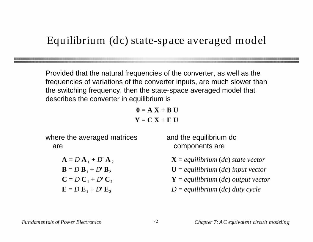
Equilibrium (dc) state-space averaged model
Provided that the natural frequencies of the converter, as well as the frequencies of variations of the converter inputs, are much slower than the switching frequency, then the state-space averaged model that describes the converter in equilibrium is
0 = A X + B UY = C X + E U
where the averaged matrices are
A = D A 1 + D' A 2
B = D B1 + D' B2
C = D C1 + D' C2
E = D E1 + D' E2
and the equilibrium dc components are
X = equilibrium (dc) state vector
U = equilibrium (dc) input vector
Y = equilibrium (dc) output vector
D = equilibrium (dc) duty cycle

Fundamentals of Power Electronics Chapter 7: AC equivalent circuit modeling73
Solution of equilibrium averaged model
X = – A– 1 B U
Y = – C A– 1 B + E U
0 = A X + B UY = C X + E U
Equilibrium state-space averaged model:
Solution for X and Y:

Fundamentals of Power Electronics Chapter 7: AC equivalent circuit modeling74
Small-signal ac state-space averaged model
K dx(t)dt
= A x(t) + B u(t) + A 1 – A 2 X + B1 – B2 U d(t)
y(t) = C x(t) + E u(t) + C1 – C2 X + E1 – E2 U d(t)
where
x(t) = small – signal (ac) perturbation in state vector
u(t) = small – signal (ac) perturbation in input vector
y(t) = small – signal (ac) perturbation in output vector
d(t) = small – signal (ac) perturbation in duty cycle
So if we can write the converter state equations during subintervals 1 and 2, then we can always find the averaged dc and small-signal ac models

Fundamentals of Power Electronics Chapter 7: AC equivalent circuit modeling75
The low-frequency components of the input and output vectors are modeled in a similar manner.
By averaging the inductor voltages and capacitor currents, one obtains:
7.4.3. Discussion of the state-space averaging result
As in Sections 7.1 and 7.2, the low-frequency components of the inductor currents and capacitor voltages are modeled by averaging over an interval of length Ts. Hence, we define the average of the state vector as:
x(t)Ts
= 1Ts
x(τ) dτt
t + Ts
Kd x(t)
Ts
dt= d(t) A 1 + d'(t) A 2 x(t)
Ts+ d(t) B1 + d'(t) B2 u(t)
Ts
Fundamentals of Power Electronics Chapter 7: AC equivalent circuit modeling76
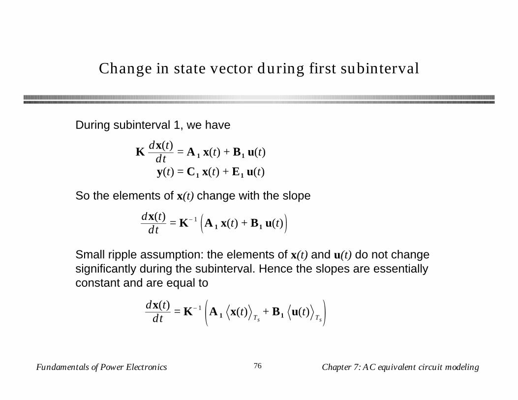
Change in state vector during first subinterval
K dx(t)dt
= A 1 x(t) + B1 u(t)
y(t) = C1 x(t) + E1 u(t)
During subinterval 1, we have
So the elements of x(t) change with the slope
dx(t)dt
= K– 1 A 1 x(t) + B1 u(t)
Small ripple assumption: the elements of x(t) and u(t) do not change significantly during the subinterval. Hence the slopes are essentially constant and are equal to
dx(t)dt
= K– 1 A 1 x(t)Ts
+ B1 u(t)Ts
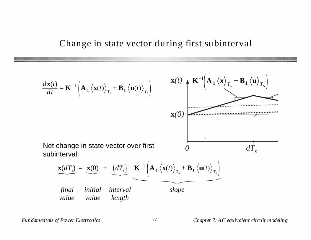
Fundamentals of Power Electronics Chapter 7: AC equivalent circuit modeling77
Change in state vector during first subinterval
dx(t)dt
= K– 1 A 1 x(t)Ts
+ B1 u(t)Ts
x(dTs) = x(0) + dTs K– 1 A 1 x(t)Ts
+ B1 u(t)Ts
final initial interval slopevalue value length
K–1 A 1 xTs
+ B1 uTs
x(t)
x(0)
dTs0
K–1 dA 1 + d'A 2 x Ts+ dB
Net change in state vector over first subinterval:

Fundamentals of Power Electronics Chapter 7: AC equivalent circuit modeling78
Change in state vector during second subinterval
Use similar arguments.
State vector now changes with the essentially constant slope
dx(t)dt
= K– 1 A 2 x(t)Ts
+ B2 u(t)Ts
The value of the state vector at the end of the second subinterval is therefore
x(Ts) = x(dTs) + d'Ts K– 1 A 2 x(t)Ts
+ B2 u(t)Ts
final initial interval slopevalue value length

Fundamentals of Power Electronics Chapter 7: AC equivalent circuit modeling79
Net change in state vector over one switching period
We have:
x(dTs) = x(0) + dTs K– 1 A 1 x(t)Ts
+ B1 u(t)Ts
x(Ts) = x(dTs) + d'Ts K– 1 A 2 x(t)Ts
+ B2 u(t)Ts
Eliminate x(dTs), to express x(Ts) directly in terms of x(0) :
x(Ts) = x(0) + dTsK– 1 A 1 x(t)
Ts+ B1 u(t)
Ts+ d'TsK
– 1 A 2 x(t)Ts
+ B2 u(t)Ts
Collect terms:
x(Ts) = x(0) + TsK– 1 d(t)A 1 + d'(t)A2 x(t)
Ts+ TsK
– 1 d(t)B1 + d'(t)B2 u(t)Ts

Fundamentals of Power Electronics Chapter 7: AC equivalent circuit modeling80
Approximate derivative of state vector
d x(t)Ts
dt≈ x(Ts) – x(0)
Ts
Kd x(t)
Ts
dt= d(t) A 1 + d'(t) A 2 x(t)
Ts+ d(t) B1 + d'(t) B2 u(t)
Ts
Use Euler approximation:
We obtain:
K–1 A 1 xTs
+ B1 uTs
K–1 A 2 xTs
+ B2 uTs
t
x(t)
x(0) x(Ts)
dTs Ts0
K–1 dA 1 + d'A 2 x Ts+ dB1 + d'B2 u Ts
x(t) Ts

Fundamentals of Power Electronics Chapter 7: AC equivalent circuit modeling81
Low-frequency components of output vector
t
y(t)
dTs Ts
00
C1 x(t)Ts
+ E1 u(t)Ts
C2 x(t)Ts
+ E2 u(t)Ts
y(t)Ts
Remove switching harmonics by averaging over one switching period:
y(t)Ts
= d(t) C1 + d'(t) C2 x(t)Ts
+ d(t) E1 + d'(t) E2 u(t)Ts
y(t)Ts
= d(t) C1 x(t)Ts
+ E1 u(t)Ts
+ d'(t) C2 x(t)Ts
+ E2 u(t)Ts
Collect terms:

Fundamentals of Power Electronics Chapter 7: AC equivalent circuit modeling82
Averaged state equations: quiescent operating point
Kd x(t)
Ts
dt= d(t) A 1 + d'(t) A 2 x(t)
Ts+ d(t) B1 + d'(t) B2 u(t)
Ts
y(t)Ts
= d(t) C1 + d'(t) C2 x(t)Ts
+ d(t) E1 + d'(t) E2 u(t)Ts
The averaged (nonlinear) state equations:
The converter operates in equilibrium when the derivatives of all elements of < x(t) >Ts
are zero. Hence, the converter quiescent operating point is the solution of
0 = A X + B UY = C X + E U
where A = D A 1 + D' A 2
B = D B1 + D' B2
C = D C1 + D' C2
E = D E1 + D' E2
X = equilibrium (dc) state vector
U = equilibrium (dc) input vector
Y = equilibrium (dc) output vector
D = equilibrium (dc) duty cycle
and
Fundamentals of Power Electronics Chapter 7: AC equivalent circuit modeling83
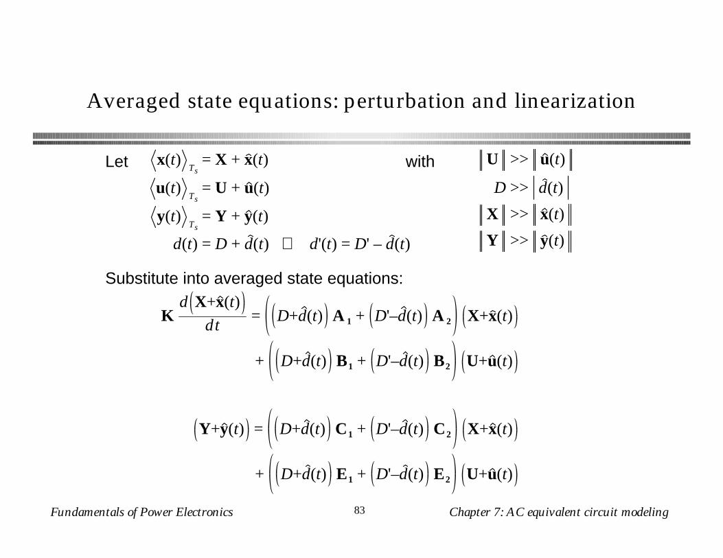
Averaged state equations: perturbation and linearization
Let x(t)Ts
= X + x(t)
u(t)Ts
= U + u(t)
y(t)Ts
= Y + y(t)
d(t) = D + d(t) ⇒ d'(t) = D' – d(t)
with U >> u(t)
D >> d(t)
X >> x(t)
Y >> y(t)
Substitute into averaged state equations:
Kd X+x(t)
dt= D+d(t) A 1 + D'–d(t) A 2 X+x(t)
+ D+d(t) B1 + D'–d(t) B2 U+u(t)
Y+y(t) = D+d(t) C1 + D'–d(t) C2 X+x(t)
+ D+d(t) E1 + D'–d(t) E2 U+u(t)
Fundamentals of Power Electronics Chapter 7: AC equivalent circuit modeling84
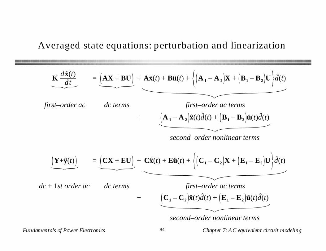
Averaged state equations: perturbation and linearization
K dx(t)dt
= AX + BU + Ax(t) + Bu(t) + A 1 – A 2 X + B1 – B2 U d(t)
first–order ac dc terms first–order ac terms
+ A 1 – A 2 x(t)d(t) + B1 – B2 u(t)d(t)
second–order nonlinear terms
Y+y(t) = CX + EU + Cx(t) + Eu(t) + C1 – C2 X + E1 – E2 U d(t)
dc + 1st order ac dc terms first–order ac terms
+ C1 – C2 x(t)d(t) + E1 – E2 u(t)d(t)
second–order nonlinear terms
Fundamentals of Power Electronics Chapter 7: AC equivalent circuit modeling85
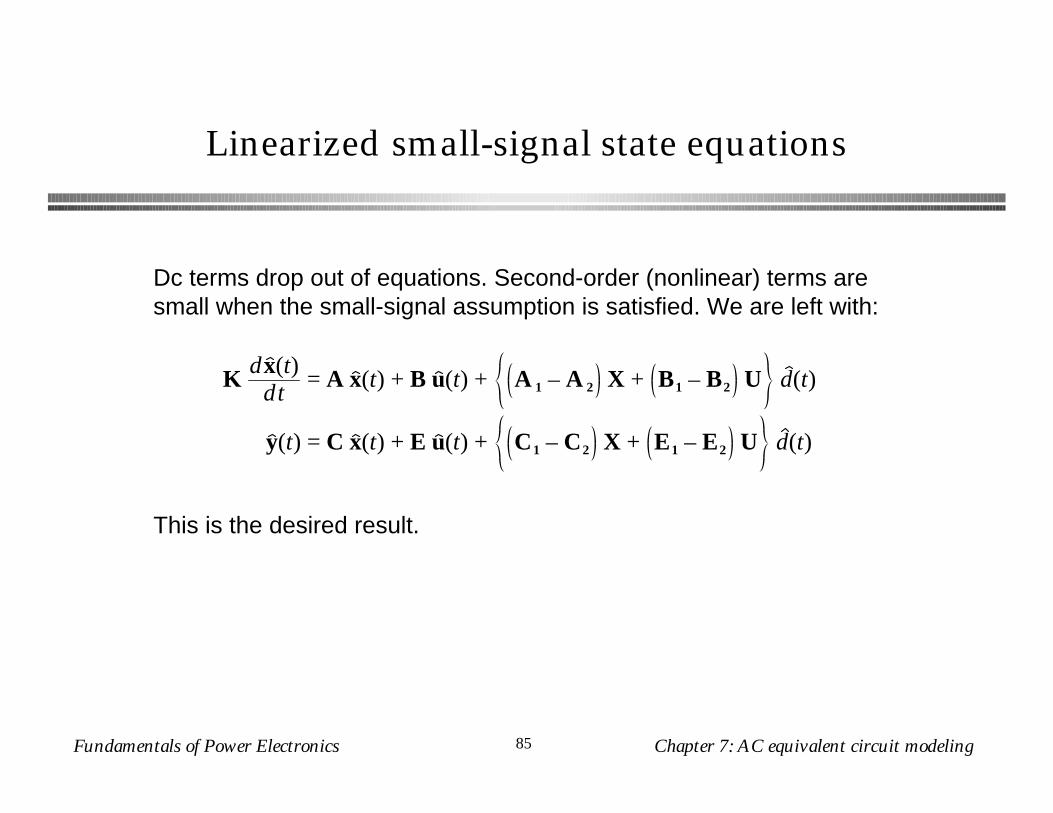
Linearized small-signal state equations
K dx(t)dt
= A x(t) + B u(t) + A 1 – A 2 X + B1 – B2 U d(t)
y(t) = C x(t) + E u(t) + C1 – C2 X + E1 – E2 U d(t)
Dc terms drop out of equations. Second-order (nonlinear) terms are small when the small-signal assumption is satisfied. We are left with:
This is the desired result.

Fundamentals of Power Electronics Chapter 7: AC equivalent circuit modeling86
7.4.4. Example: State-space averaging of a nonideal buck-boost converter
+– L C R
+
v(t)
–
vg(t)
Q1 D1
i(t)
ig(t) Model nonidealities:
• MOSFET on-resistance Ron
• Diode forward voltage drop VD
x(t) =i(t)v(t) u(t) =
vg(t)VD
y(t) = ig(t)
state vector input vector output vector
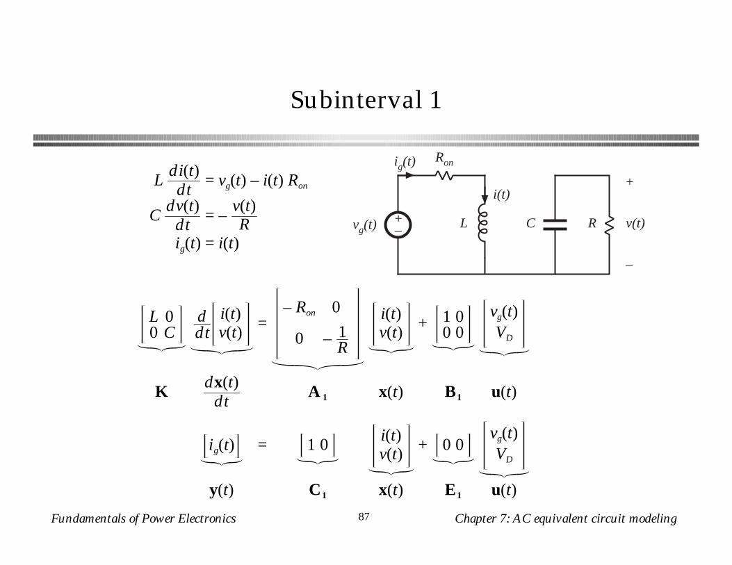
Fundamentals of Power Electronics Chapter 7: AC equivalent circuit modeling87
Subinterval 1
+– L C R
+
v(t)
–
i(t)
vg(t)
Ronig(t)
Ldi(t)dt
= vg(t) – i(t) Ron
Cdv(t)
dt= –
v(t)R
ig(t) = i(t)
L 00 C
ddt
i(t)v(t) =
– Ron 0
0 – 1R
i(t)v(t) + 1 0
0 0vg(t)VD
K dx(t)dt
A 1 x(t) B1 u(t)
ig(t) = 1 0i(t)v(t) + 0 0
vg(t)VD
y(t) C1 x(t) E1 u(t)
Fundamentals of Power Electronics Chapter 7: AC equivalent circuit modeling88
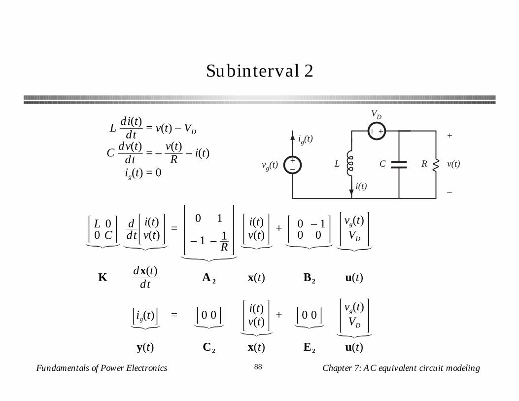
Subinterval 2
+– L C R
+
v(t)
–i(t)
vg(t)
+–
VD
ig(t)L
di(t)dt
= v(t) – VD
Cdv(t)
dt= –
v(t)R – i(t)
ig(t) = 0
L 00 C
ddt
i(t)v(t) =
0 1
– 1 – 1R
i(t)v(t) + 0 – 1
0 0vg(t)VD
K dx(t)dt
A 2 x(t) B2 u(t)
ig(t) = 0 0i(t)v(t) + 0 0
vg(t)VD
y(t) C2 x(t) E2 u(t)

Fundamentals of Power Electronics Chapter 7: AC equivalent circuit modeling89
Evaluate averaged matrices
A = DA 1 + D'A 2 = D– Ron 0
0 – 1R
+ D'0 1
– 1 – 1R
=– DRon D'
– D' – 1R
B = DB1 + D'B2 = D – D'0 0
C = DC1 + D'C2 = D 0
E = DE1 + D'E2 = 0 0
In a similar manner,
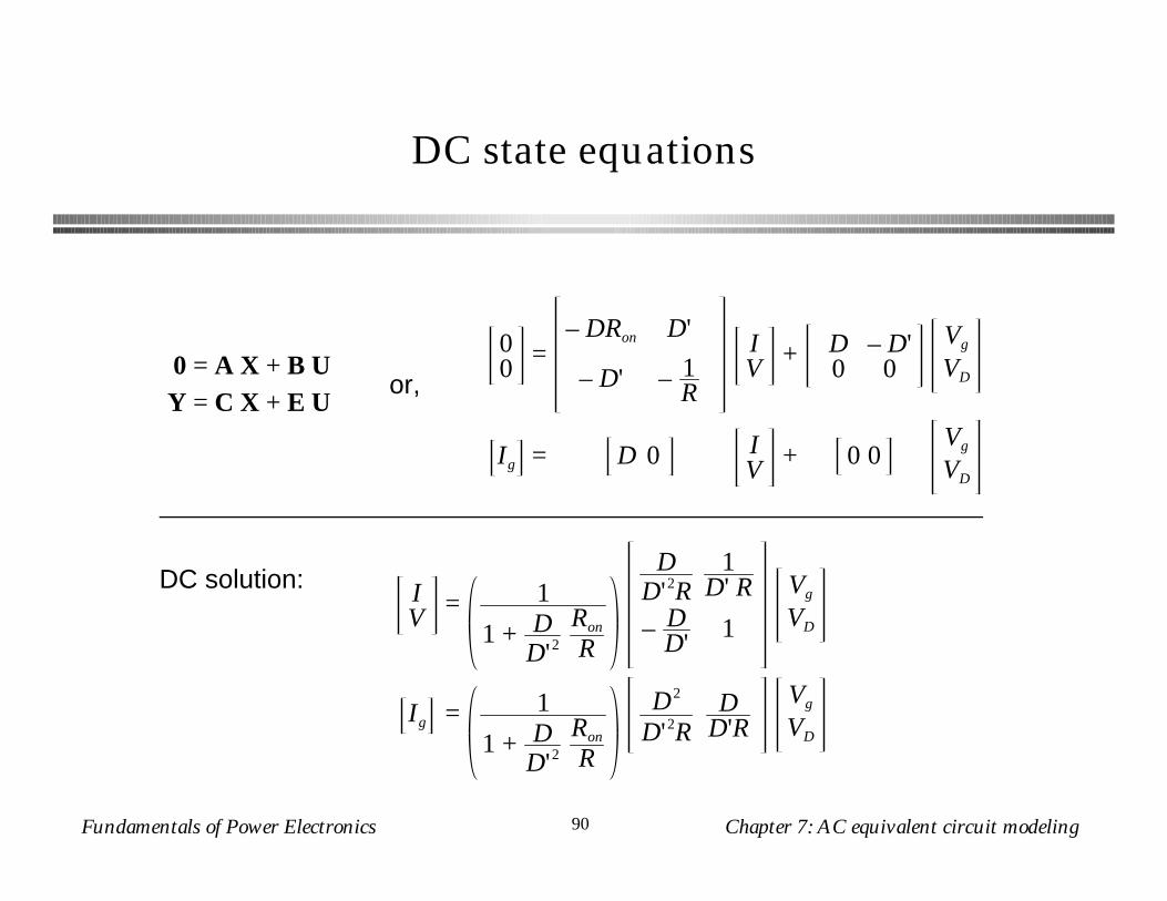
Fundamentals of Power Electronics Chapter 7: AC equivalent circuit modeling90
DC state equations
00 =
– DRon D'
– D' – 1R
IV + D – D'
0 0Vg
VD
Ig = D 0 IV + 0 0
Vg
VD
0 = A X + B UY = C X + E U
or,
IV = 1
1 + DD'2
Ron
R
DD'2R
1D' R
– DD'
1
Vg
VD
Ig = 1
1 + DD'2
Ron
R
D2
D'2RD
D'RVg
VD
DC solution:
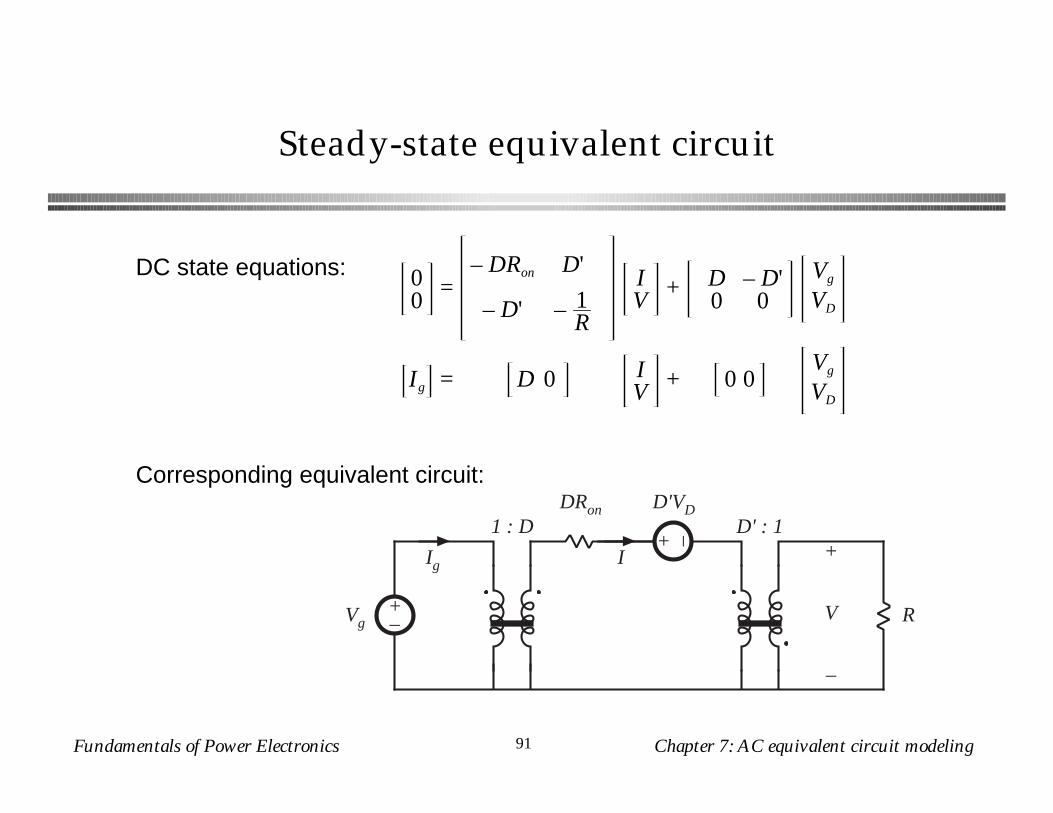
Fundamentals of Power Electronics Chapter 7: AC equivalent circuit modeling91
Steady-state equivalent circuit
+–
+ –
Vg
Ig I
R
1 : D D' : 1DRon D'VD
+
V
–
00 =
– DRon D'
– D' – 1R
IV + D – D'
0 0Vg
VD
Ig = D 0 IV + 0 0
Vg
VD
DC state equations:
Corresponding equivalent circuit:
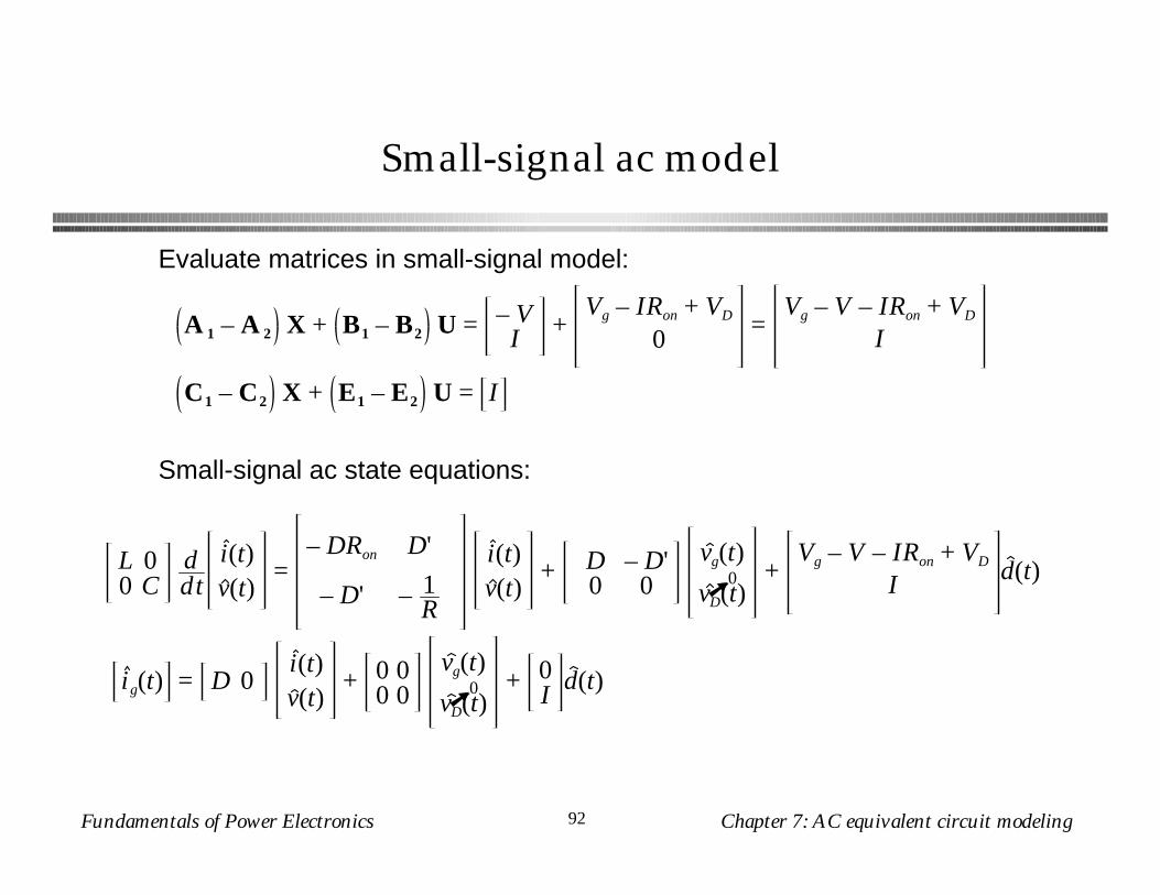
Fundamentals of Power Electronics Chapter 7: AC equivalent circuit modeling92
Small-signal ac model
Evaluate matrices in small-signal model:
A 1 – A 2 X + B1 – B2 U = – VI +
Vg – IRon + VD
0 =Vg – V – IRon + VD
I
C1 – C2 X + E1 – E2 U = I
Small-signal ac state equations:
L 00 C
ddt
i(t)v(t)
=– DRon D'
– D' – 1R
i(t)v(t)
+ D – D'0 0
vg(t)
vD(t)➚0 +
Vg – V – IRon + VD
I d(t)
ig(t) = D 0i(t)v(t)
+ 0 00 0
vg(t)
vD(t)➚0 + 0
I d(t)

Fundamentals of Power Electronics Chapter 7: AC equivalent circuit modeling93
Construction of ac equivalent circuit
Ldi(t)dt
= D' v(t) – DRon i(t) + D vg(t) + Vg – V – IRon + VD d(t)
Cdv(t)
dt= –D' i(t) –
v(t)R + I d(t)
ig(t) = D i(t) + I d(t)
Small-signal ac equations, in scalar form:
+–
+–
+–
L
D' v(t)
d(t) Vg – V + VD – IRon
Ld i(t)
dt
D vg(t)i(t)
+ –
DRon
+
v(t)
–
RC
Cdv(t)
dt
D' i(t) I d(t)
v(t)R
+– D i(t)I d(t)
i g(t)
vg(t)
Corresponding equivalent circuits:
inductor equation
input eqn
capacitor eqn
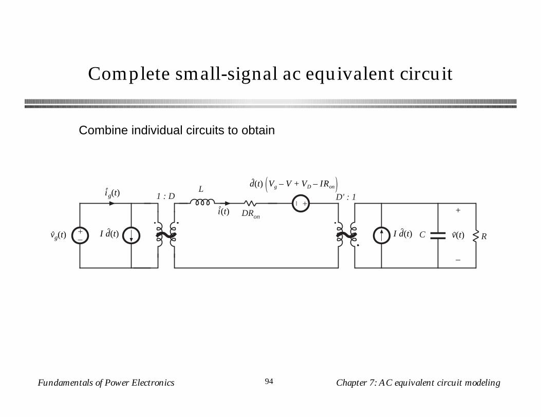
Fundamentals of Power Electronics Chapter 7: AC equivalent circuit modeling94
Complete small-signal ac equivalent circuit
+–
I d(t)
i g(t)
vg(t)
Ld(t) Vg – V + VD – IRon
i(t) DRon+
v(t)
–
RCI d(t)
1 : D +– D' : 1
Combine individual circuits to obtain

Fundamentals of Power Electronics Chapter 7: AC equivalent circuit modeling95
7.5. Circuit Averaging and Averaged Switch Modeling
● Historically, circuit averaging was the first method known for modeling the small-signal ac behavior of CCM PWM converters
● It was originally thought to be difficult to apply in some cases● There has been renewed interest in circuit averaging and its
corrolary, averaged switch modeling, in the last decade● Can be applied to a wide variety of converters
● We will use it to model DCM, CPM, and resonant converters
● Also useful for incorporating switching loss into ac model of CCM converters
● Applicable to 3ø PWM inverters and rectifiers
● Can be applied to phase-controlled rectifiers
● Rather than averaging and linearizing the converter state equations, the averaging and linearization operations are performed directly on the converter circuit

Fundamentals of Power Electronics Chapter 7: AC equivalent circuit modeling96
Separate switch network from remainder of converter
+–
Time-invariant networkcontaining converter reactive elements
C L
+ vC(t) –iL(t)
R
+
v(t)
–
vg(t)
Power input Load
Switch network
po
rt 1
po
rt 2
d(t)Controlinput
+
v1(t)
–
+
v2(t)
–
i1(t) i2(t)

Fundamentals of Power Electronics Chapter 7: AC equivalent circuit modeling97
Boost converter example
+–
L
C R
+
v(t)
–
vg(t)
i(t)
+
v1(t)
–
+
v2(t)
–
i1(t) i2(t)
+
v1(t)
–
+
v2(t)
–
i1(t) i2(t)
Ideal boost converter example
Two ways to define the switch network
(a) (b)
Fundamentals of Power Electronics Chapter 7: AC equivalent circuit modeling98
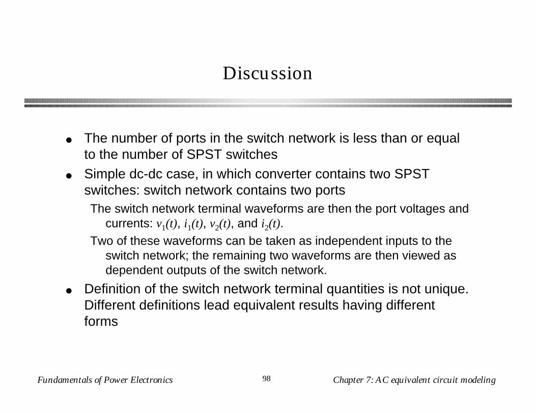
Discussion
● The number of ports in the switch network is less than or equal to the number of SPST switches
● Simple dc-dc case, in which converter contains two SPST switches: switch network contains two portsThe switch network terminal waveforms are then the port voltages and
currents: v1(t), i1(t), v2(t), and i2(t). Two of these waveforms can be taken as independent inputs to the
switch network; the remaining two waveforms are then viewed as dependent outputs of the switch network.
● Definition of the switch network terminal quantities is not unique. Different definitions lead equivalent results having different forms

Fundamentals of Power Electronics Chapter 7: AC equivalent circuit modeling99
Boost converter example
Let’s use definition (a):
+–
L
C R
+
v(t)
–
vg(t)
i(t)+
v1(t)
–
+
v2(t)
–
i1(t) i2(t)
Since i1(t) and v2(t) coincide with the converter inductor current and output voltage, it is convenient to define these waveforms as the independent inputs to the switch network. The switch network dependent outputs are then v1(t) and i2(t).

Fundamentals of Power Electronics Chapter 7: AC equivalent circuit modeling100
Obtaining a time-invariant network:Modeling the terminal behavior of the switch network
Replace the switch network with dependent sources, which correctly represent the dependent output waveforms of the switch network
+–
+–
L
C R
+
v(t)
–
vg(t)
i(t)
v1(t)
+
v2(t)
–
i1(t)
i2(t)
Switch network
Boost converter example

Fundamentals of Power Electronics Chapter 7: AC equivalent circuit modeling101
Definition of dependent generator waveforms
t
v1(t)
dTs Ts
00
0
v2(t)
t
i2(t)
dTs Ts
00
0
i1(t)
⟨v1(t)⟩Ts
⟨i2(t)⟩Ts
+–
+–
L
C R
+
v(t)
–
vg(t)
i(t)
v1(t)
+
v2(t)
–
i1(t)
i2(t)
Switch network
The waveforms of the dependent generators are defined to be identical to the actual terminal waveforms of the switch network.
The circuit is therefore electrical identical to the original converter.
So far, no approximations have been made.
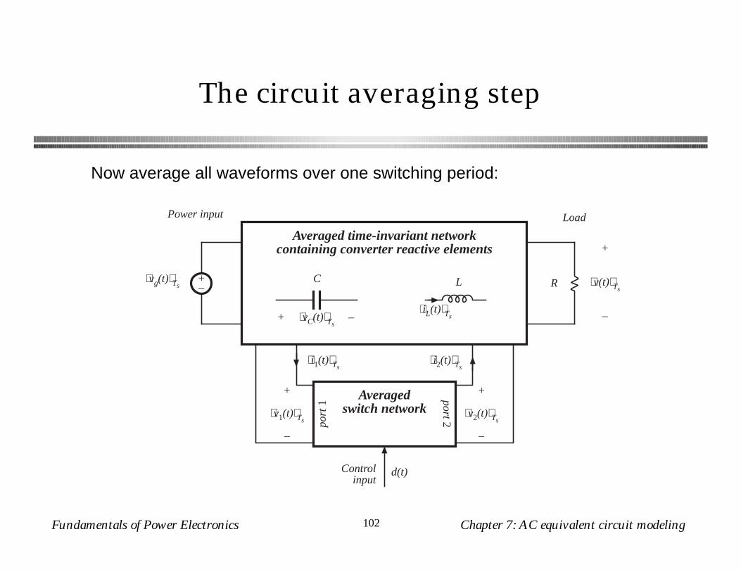
Fundamentals of Power Electronics Chapter 7: AC equivalent circuit modeling102
The circuit averaging step
+–
Averaged time-invariant networkcontaining converter reactive elements
C L
+ ⟨vC(t)⟩Ts –
⟨iL(t)⟩Ts
R
+
⟨v(t)⟩Ts
–
⟨vg(t)⟩Ts
Power input Load
Averagedswitch network
po
rt 1
po
rt 2
d(t)Controlinput
+
⟨v2(t)⟩Ts
–
⟨i1(t)⟩Ts⟨i2(t)⟩Ts
+
⟨v1(t)⟩Ts
–
Now average all waveforms over one switching period:

Fundamentals of Power Electronics Chapter 7: AC equivalent circuit modeling103
The averaging step
The basic assumption is made that the natural time constants of the converter are much longer than the switching period, so that the converter contains low-pass filtering of the switching harmonics. One may average the waveforms over an interval that is short compared to the system natural time constants, without significantly altering the system response. In particular, averaging over the switching period Ts removes the switching harmonics, while preserving the low-frequency components of the waveforms.
In practice, the only work needed for this step is to average the switch dependent waveforms.
Fundamentals of Power Electronics Chapter 7: AC equivalent circuit modeling104
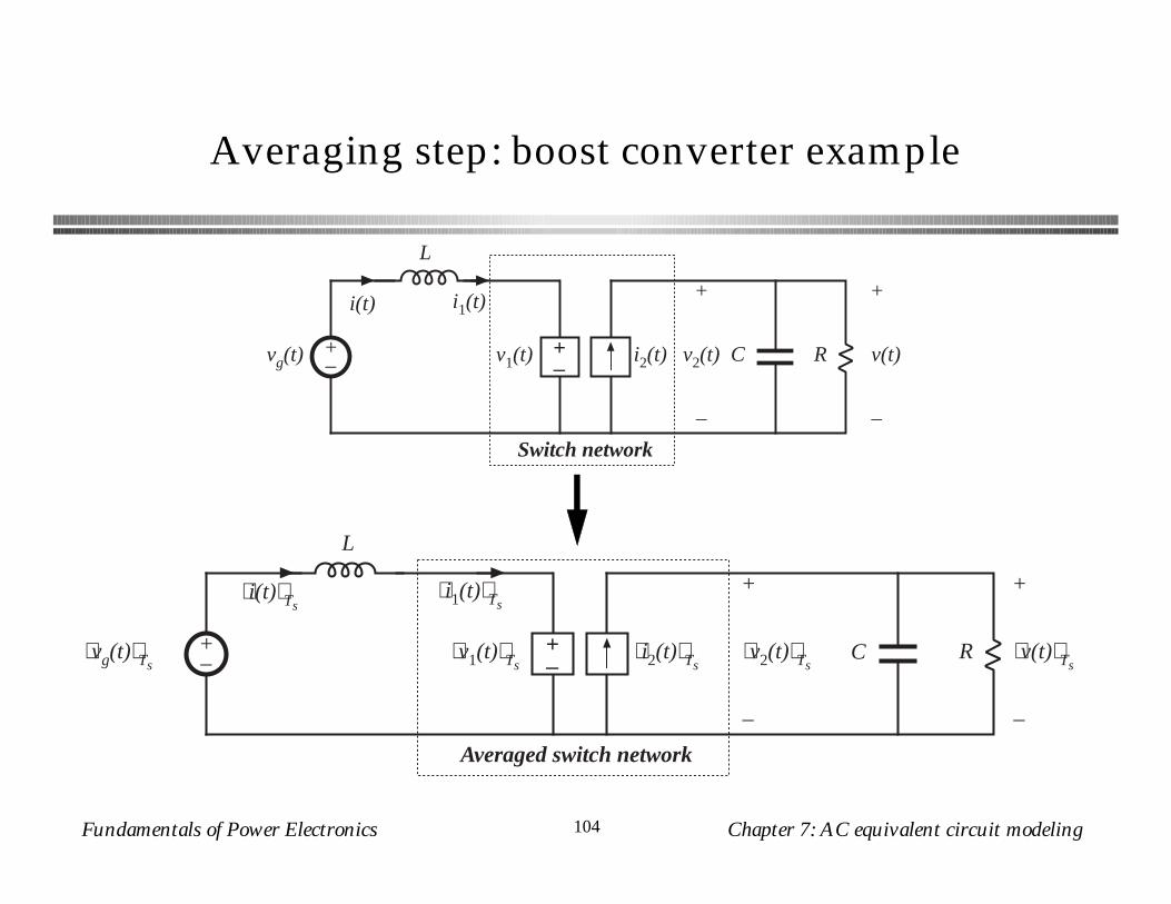
Averaging step: boost converter example
+–
+–
L
C R
+
v(t)
–
vg(t)
i(t)
v1(t)
+
v2(t)
–
i1(t)
i2(t)
Switch network
+–
+–
L
C R
+
⟨v(t)⟩Ts
–
⟨vg(t)⟩Ts⟨v1(t)⟩Ts
⟨i2(t)⟩Ts
⟨i(t)⟩Ts
+
⟨v2(t)⟩Ts
–
⟨i1(t)⟩Ts
Averaged switch network
Fundamentals of Power Electronics Chapter 7: AC equivalent circuit modeling105
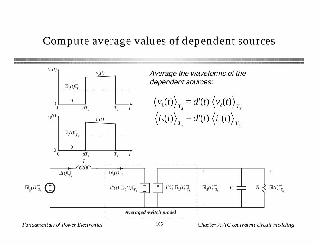
Compute average values of dependent sources
t
v1(t)
dTs Ts
00
0
v2(t)
t
i2(t)
dTs Ts
00
0
i1(t)
⟨v1(t)⟩Ts
⟨i2(t)⟩Ts
+–
+–
L
C R
+
⟨v(t)⟩Ts
–
⟨vg(t)⟩Tsd'(t) ⟨v2(t)⟩Ts
d'(t) ⟨i1(t)⟩Ts
⟨i(t)⟩Ts
+
⟨v2(t)⟩Ts
–
⟨i1(t)⟩Ts
Averaged switch model
v1(t) Ts= d'(t) v2(t) Ts
i2(t) Ts= d'(t) i1(t) Ts
Average the waveforms of the dependent sources:

Fundamentals of Power Electronics Chapter 7: AC equivalent circuit modeling106
Perturb and linearize
vg(t) Ts= Vg + vg(t)
d(t) = D + d(t) ⇒ d'(t) = D' – d(t)
i(t)Ts
= i1(t) Ts= I + i(t)
v(t)Ts
= v2(t) Ts= V + v(t)
v1(t) Ts= V1 + v1(t)
i2(t) Ts= I2 + i2(t)
+–
+–
L
C R
+
–
Vg + vg(t)
I + i(t)
D' – d(t) V + v(t) D' – d(t) I + i(t) V + v(t)
As usual, let:
The circuit becomes:

Fundamentals of Power Electronics Chapter 7: AC equivalent circuit modeling107
Dependent voltage source
+–
+–
V d(t)
D' V + v(t)
D' – d(t) V + v(t) = D' V + v(t) – V d(t) – v(t)d(t)
nonlinear,2nd order

Fundamentals of Power Electronics Chapter 7: AC equivalent circuit modeling108
Dependent current source
D' – d(t) I + i(t) = D' I + i(t) – Id(t) – i(t)d(t)
nonlinear,2nd order
D' I + i(t) I d(t)

Fundamentals of Power Electronics Chapter 7: AC equivalent circuit modeling109
Linearized circuit-averaged model
+–
L
C R
+
–
Vg + vg(t)
I + i(t)
V + v(t)+–
+–
V d(t)
D' V + v(t) D' I + i(t) I d(t)
+–
L
C R
+
–
Vg + vg(t)
I + i(t)
V + v(t)
+–
V d(t)
I d(t)
D' : 1

Fundamentals of Power Electronics Chapter 7: AC equivalent circuit modeling110
Summary: Circuit averaging method
Model the switch network with equivalent voltage and current sources, such that an equivalent time-invariant network is obtained
Average converter waveforms over one switching period, to remove the switching harmonics
Perturb and linearize the resulting low-frequency model, to obtain a small-signal equivalent circuit

Fundamentals of Power Electronics Chapter 7: AC equivalent circuit modeling111
Averaged switch modeling: CCM
I + i(t)
+–
V d(t)
I d(t)
D' : 1
+
–
V + v(t)
+
v(t)
–
1
2
i(t)
Switchnetwork
Circuit averaging of the boost converter: in essence, the switch network was replaced with an effective ideal transformer and generators:

Fundamentals of Power Electronics Chapter 7: AC equivalent circuit modeling112
Basic functions performed by switch network
I + i(t)
+–
V d(t)
I d(t)
D' : 1
+
–
V + v(t)
+
v(t)
–
1
2
i(t)
Switchnetwork
For the boost example, we can conclude that the switch network performs two basic functions:
• Transformation of dc and small-signal ac voltage and current levels, according to the D’:1 conversion ratio
• Introduction of ac voltage and current variations, drive by the control input duty cycle variations
Circuit averaging modifies only the switch network. Hence, to obtain a small-signal converter model, we need only replace the switch network with its averaged model. Such a procedure is called averaged switch modeling.
Fundamentals of Power Electronics Chapter 7: AC equivalent circuit modeling113
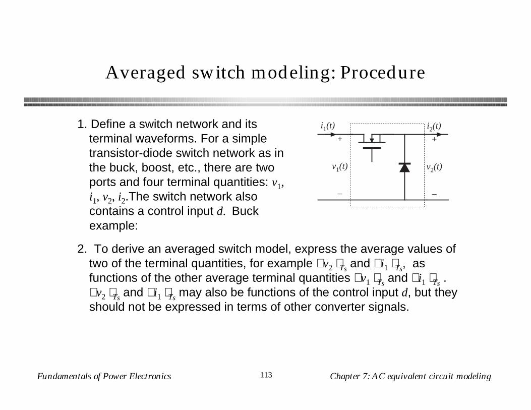
Averaged switch modeling: Procedure
+
v2(t)
–
i1(t) i2(t)
+
v1(t)
–
1. Define a switch network and its terminal waveforms. For a simple transistor-diode switch network as in the buck, boost, etc., there are two ports and four terminal quantities: v1, i1, v2, i2.The switch network also contains a control input d. Buck example:
2. To derive an averaged switch model, express the average values of two of the terminal quantities, for example ⟨ v2 ⟩Ts and ⟨ i1 ⟩Ts, as functions of the other average terminal quantities ⟨ v1 ⟩Ts and ⟨ i1 ⟩Ts . ⟨ v2 ⟩Ts and ⟨ i1 ⟩Ts may also be functions of the control input d, but they should not be expressed in terms of other converter signals.

Fundamentals of Power Electronics Chapter 7: AC equivalent circuit modeling114
The basic buck-type CCM switch cell
+–
L
C R
+
v(t)
–
vg(t)
i(t)
+
v2(t)
–
i1(t) i2(t)
Switch network
+
v1(t)
–
iC+ vCE –
t
i1(t)
dTs Ts
00
i1(t) T2
0
i2
i2 T2
t
v2(t)
dTs Ts
00
v2(t) T2
0
v1i1(t) Ts= d(t) i2(t) Ts
v2(t) Ts= d(t) v1(t) Ts
Fundamentals of Power Electronics Chapter 7: AC equivalent circuit modeling115
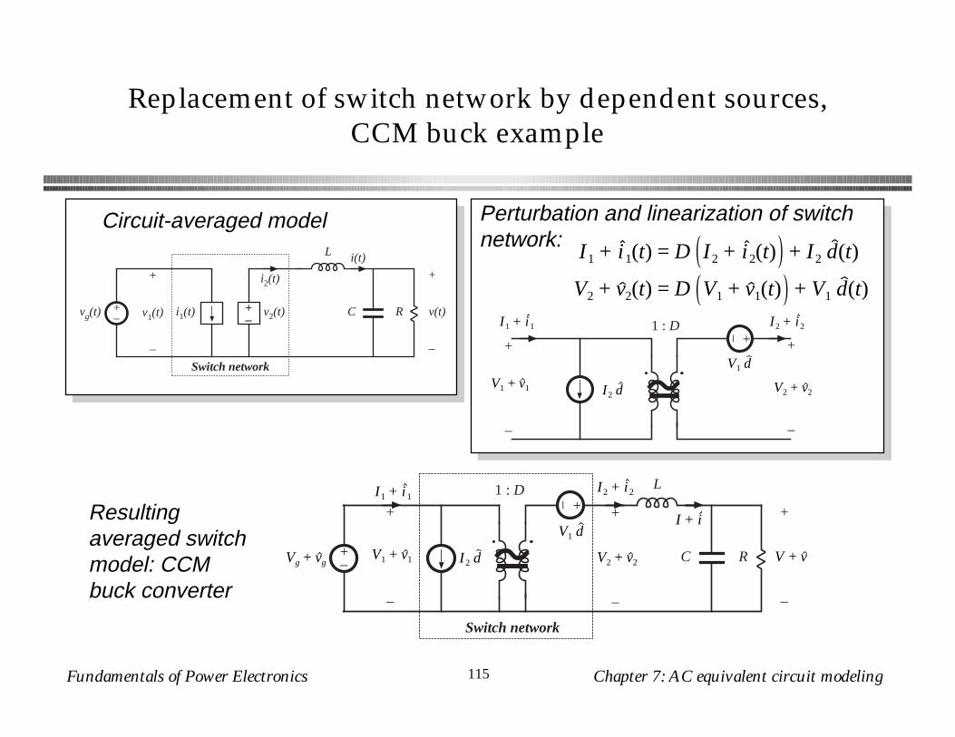
Replacement of switch network by dependent sources, CCM buck example
I1 + i1(t) = D I2 + i2(t) + I2 d(t)
V2 + v2(t) = D V1 + v1(t) + V1 d(t)
Perturbation and linearization of switch network:
+–1 : DI1 + i1 I2 + i2
I2 dV1 + v1
V1 d
V2 + v2
+
–
+
–
+–
L
C R
Switch network
+–1 : DI1 + i1I2 + i2
I2 dV1 + v1
V1 d
V2 + v2
+
–
+
–
I + i
V + v
+
–
Vg + vg
+–
L
C R
+
v(t)
–
vg(t)
i(t)
i1(t)
i2(t)+
v1(t)
–
+–
v2(t)
Switch network
Circuit-averaged model
Resulting averaged switch model: CCM buck converter
Fundamentals of Power Electronics Chapter 7: AC equivalent circuit modeling116
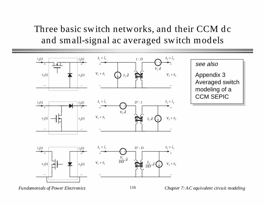
Three basic switch networks, and their CCM dc and small-signal ac averaged switch models
+
v2(t)
–
i1(t) i2(t)
+
v1(t)
–
+–1 : DI1 + i1 I2 + i2
I2 dV1 + v1
V1 d
V2 + v2
+
–
+
–
+– D' : 1I1 + i1 I2 + i2
I1 dV1 + v1
V2 d
V2 + v2
+
–
+
–
+
v2(t)
–
i1(t) i2(t)
+
v1(t)
–
+
v2(t)
–
i1(t) i2(t)
+
v1(t)
–
+– D' : DI1 + i1 I2 + i2
I2
DD'dV1 + v1
V1
DD'd
V2 + v2
+
–
+
–
see also
Appendix 3 Averaged switch modeling of a CCM SEPIC

Fundamentals of Power Electronics Chapter 7: AC equivalent circuit modeling117
Example: Averaged switch modeling of CCM buck converter, including switching loss
+–
L
C R
+
v(t)
–
vg(t)
i(t)
+
v2(t)
–
i1(t) i2(t)
Switch network
+
v1(t)
–
iC+ vCE –
t
iC(t)
Ts
0
i2
vCE(t)
v1
0
t1 t2tir tvf tvr tif
i1(t) = iC(t)v2(t) = v1(t) – vCE(t)
Switch network terminal waveforms: v1, i1, v2, i2. To derive averaged switch model, express ⟨ v2 ⟩Ts and ⟨ i1 ⟩Ts as functions of ⟨ v1 ⟩Ts and ⟨ i1 ⟩Ts . ⟨ v2 ⟩Ts and ⟨ i1 ⟩Ts may also be functions of the control input d, but they should not be expressed in terms of other converter signals.

Fundamentals of Power Electronics Chapter 7: AC equivalent circuit modeling118
Averaging i1(t)
i1(t) Ts= 1
Tsi1(t) dt
0
Ts
= i2(t) Ts
t1 + tvf + tvr + 12
tir + 12
tif
Ts
t
iC(t)
Ts
0
i2
vCE(t)
v1
0
t1 t2tir tvf tvr tif

Fundamentals of Power Electronics Chapter 7: AC equivalent circuit modeling119
Expression for ⟨ i1(t) ⟩
d =t1 + 1
2tvf + 1
2tvr + 1
2tir + 1
2tif
Ts
dv =tvf + tvr
Ts
di =tir + tif
Ts
i1(t) Ts= 1
Tsi1(t) dt
0
Ts
= i2(t) Ts
t1 + tvf + tvr + 12
tir + 12
tif
Ts
Let
Given
i1(t) Ts= i2(t) Ts
d + 12
dv
Then we can write

Fundamentals of Power Electronics Chapter 7: AC equivalent circuit modeling120
Averaging the switch network output voltage v2(t)
t
iC(t)
Ts
0
i2
vCE(t)
v1
0
t1 t2tir tvf tvr tif
v2(t) Ts= v1(t) – vCE(t)
Ts= 1
Ts– vCE(t) dt
0
Ts
+ v1(t) Ts
v2(t) Ts= v1(t) Ts
t1 + 12
tvf + 12
tvr
Ts
v2(t) Ts= v1(t) Ts
d – 12
di

Fundamentals of Power Electronics Chapter 7: AC equivalent circuit modeling121
Construction of large-signal averaged-switch model
v2(t) Ts= v1(t) Ts
d – 12
dii1(t) Ts= i2(t) Ts
d + 12
dv
+–
d(t) ⟨i2(t)⟩Tsd(t) ⟨v1(t)⟩Ts
+
⟨v2(t)⟩Ts
–
⟨i1(t)⟩Ts
+
⟨v1(t)⟩Ts
–
+ – ⟨i2(t)⟩Ts
dv(t) ⟨i2(t)⟩Ts
12
di(t) ⟨v1(t)⟩Ts
12
+
⟨v2(t)⟩Ts
–
⟨i1(t)⟩Ts
+
⟨v1(t)⟩Ts
–
+ – ⟨i2(t)⟩Ts1 : d(t)
dv(t) ⟨i2(t)⟩Ts
12
di(t) ⟨v1(t)⟩Ts
12

Fundamentals of Power Electronics Chapter 7: AC equivalent circuit modeling122
Switching loss predicted by averaged switch model
+
⟨v2(t)⟩Ts
–
⟨i1(t)⟩Ts
+
⟨v1(t)⟩Ts
–
+ – ⟨i2(t)⟩Ts1 : d(t)
dv(t) ⟨i2(t)⟩Ts
12
di(t) ⟨v1(t)⟩Ts
12
Psw = 12 dv + di i2(t) Ts
v1(t) Ts

Fundamentals of Power Electronics Chapter 7: AC equivalent circuit modeling123
Solution of averaged converter model in steady state
+
V2
–
I1
Dv I212
+
V1
–
+ – I21 : D
+–
L
C RVg
I
+
V
–
Averaged switch network model
Di V112
V = D – 12 Di Vg = DVg 1 –
Di
2D
Pin = VgI1 = V1I2 D + 12Dv
Pout = VI2 = V1I2 D – 12Di
η =Pout
Pin
=D – 1
2 Di
D + 12 Dv
=1 –
Di
2D
1 +Dv
2D
Output voltage: Efficiency calcuation:

Fundamentals of Power Electronics Chapter 7: AC equivalent circuit modeling124
7.6. The canonical circuit model
All PWM CCM dc-dc converters perform the same basic functions:
• Transformation of voltage and current levels, ideally with 100% efficiency
• Low-pass filtering of waveforms
• Control of waveforms by variation of duty cycle
Hence, we expect their equivalent circuit models to be qualitatively similar.
Canonical model:
• A standard form of equivalent circuit model, which represents the above physical properties
• Plug in parameter values for a given specific converter

Fundamentals of Power Electronics Chapter 7: AC equivalent circuit modeling125
7.6.1. Development of the canonical circuit model
+–
1 : M(D)
R
+
–
Controlinput
Powerinput
Load
D
VVg
Converter model1. Transformation of dc voltage and current levels
• modeled as in Chapter 3 with ideal dc transformer
• effective turns ratio M(D)
• can refine dc model by addition of effective loss elements, as in Chapter 3
Fundamentals of Power Electronics Chapter 7: AC equivalent circuit modeling126
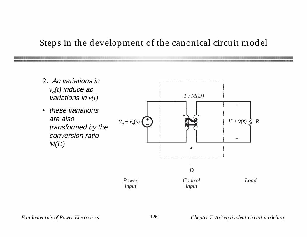
Steps in the development of the canonical circuit model
+–
1 : M(D)
RVg + vg(s)
+
–
V + v(s)
Controlinput
Powerinput
Load
D
2. Ac variations in vg(t) induce ac variations in v(t)
• these variations are also transformed by the conversion ratio M(D)

Fundamentals of Power Electronics Chapter 7: AC equivalent circuit modeling127
Steps in the development of the canonical circuit model
+–
1 : M(D)
RVg + vg(s)
+
–
V + v(s)
Effective
low-pass
filter
He(s)
Zei(s) Zeo(s)
Controlinput
Powerinput
Load
D
3. Converter must contain an effective low-pass filter characteristic
• necessary to filter switching ripple
• also filters ac variations
• effective filter elements maynot coincide with actual element values, but can also depend on operating point
Fundamentals of Power Electronics Chapter 7: AC equivalent circuit modeling128
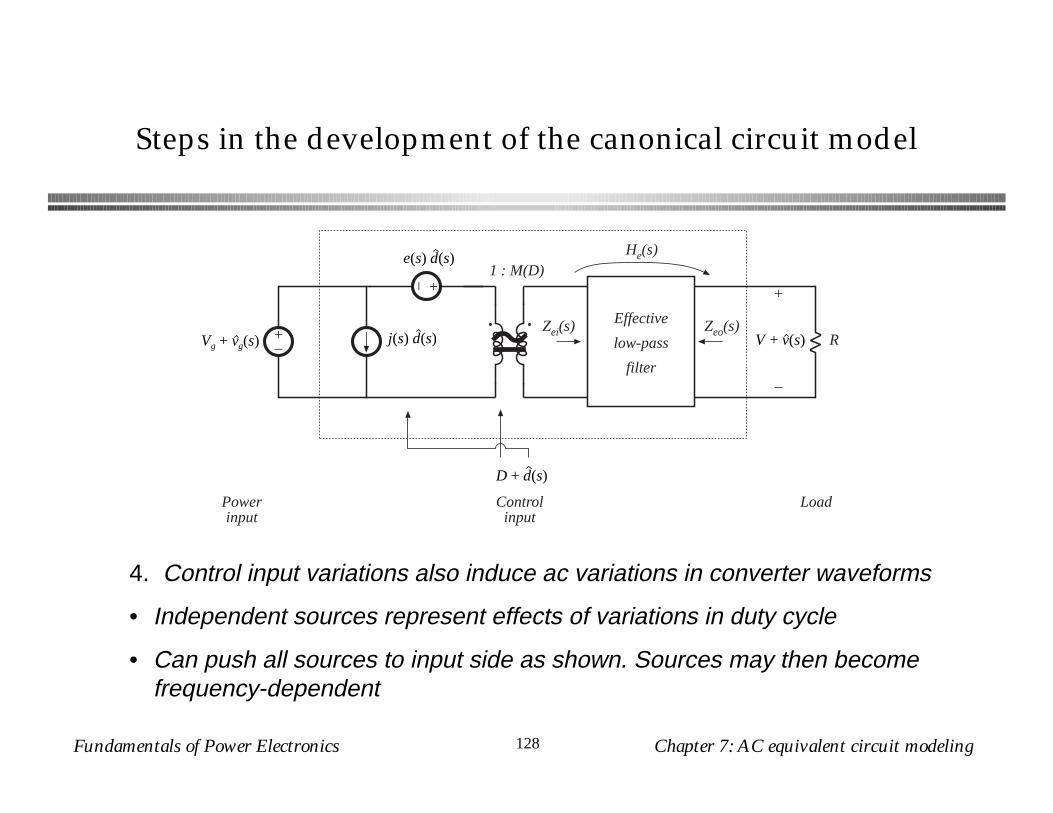
Steps in the development of the canonical circuit model
+–
+– 1 : M(D)
RVg + vg(s)
+
–
V + v(s)
e(s) d(s)
j(s) d(s)Effective
low-pass
filter
He(s)
Zei(s) Zeo(s)
Controlinput
D + d(s)
Powerinput
Load
4. Control input variations also induce ac variations in converter waveforms
• Independent sources represent effects of variations in duty cycle
• Can push all sources to input side as shown. Sources may then become frequency-dependent

Fundamentals of Power Electronics Chapter 7: AC equivalent circuit modeling129
Transfer functions predicted by canonical model
+–
+– 1 : M(D)
RVg + vg(s)
+
–
V + v(s)
e(s) d(s)
j(s) d(s)Effective
low-pass
filter
He(s)
Zei(s) Zeo(s)
Controlinput
D + d(s)
Powerinput
Load
Gvg(s) =v(s)vg(s)
= M(D) He(s)
Gvd(s) =v(s)d(s)
= e(s) M(D) He(s)
Line-to-output transfer function:
Control-to-output transfer function:
Fundamentals of Power Electronics Chapter 7: AC equivalent circuit modeling130
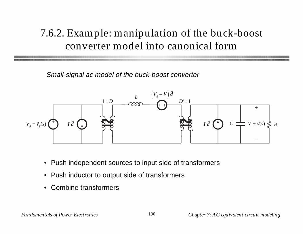
7.6.2. Example: manipulation of the buck-boost converter model into canonical form
+– I dVg + vg(s)
+–
LVg – V d
RCI d
1 : D D' : 1
V + v(s)
+
–
Small-signal ac model of the buck-boost converter
• Push independent sources to input side of transformers
• Push inductor to output side of transformers
• Combine transformers
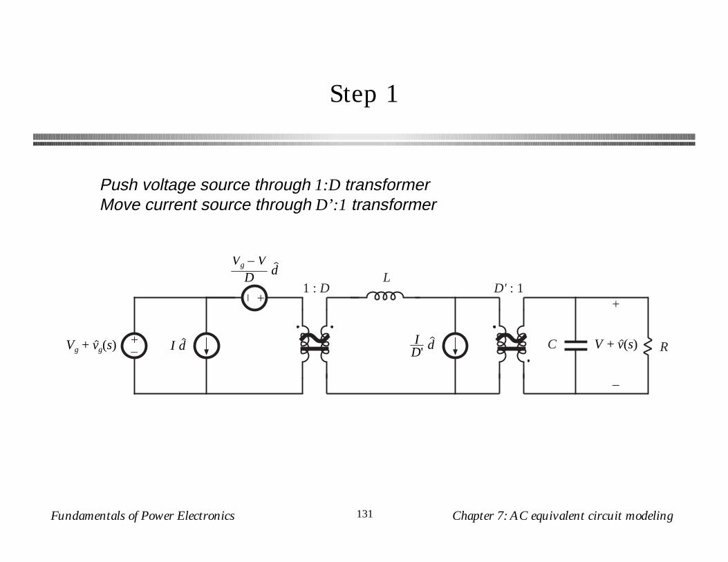
Fundamentals of Power Electronics Chapter 7: AC equivalent circuit modeling131
Step 1
+– I dVg + vg(s)
+–
L
RC
1 : D D' : 1
Vg – VD
d
ID'
d V + v(s)
+
–
Push voltage source through 1:D transformerMove current source through D’:1 transformer

Fundamentals of Power Electronics Chapter 7: AC equivalent circuit modeling132
Step 2
+– I dVg + vg(s)
+–
L
RC
1 : D D' : 1
Vg – VD
d
ID'
dV + v(s)
+
–
ID'
d
nodeA
How to move the current source past the inductor:Break ground connection of current source, and connect to node A
instead.Connect an identical current source from node A to ground, so that
the node equations are unchanged.

Fundamentals of Power Electronics Chapter 7: AC equivalent circuit modeling133
Step 3
+– I dVg + vg(s)
+–
L
RC
1 : D D' : 1
Vg – VD
d
V + v(s)
+
–
ID'
d
+ –
sLID'
d
The parallel-connected current source and inductor can now be replaced by a Thevenin-equivalent network:

Fundamentals of Power Electronics Chapter 7: AC equivalent circuit modeling134
Step 4
+–
I dVg + vg(s)+–
L
RC
1 : D D' : 1
Vg – VD
d
V + v(s)
+
–
+ –
sLID'
d
DID'
d
nodeB
DID'
d
Now push current source through 1:D transformer.
Push current source past voltage source, again by:Breaking ground connection of current source, and connecting to
node B instead.Connecting an identical current source from node B to ground, so
that the node equations are unchanged.Note that the resulting parallel-connected voltage and current
sources are equivalent to a single voltage source.

Fundamentals of Power Electronics Chapter 7: AC equivalent circuit modeling135
Step 5: final result
+–
+– D' : D
C RVg + vg(s)
+
–
V + v(s)
Vg – VD
– s LIDD'
d(s)
ID'
d(s)
LD'2
Effectivelow-pass
filter
Push voltage source through 1:D transformer, and combine with existing input-side transformer.
Combine series-connected transformers.

Fundamentals of Power Electronics Chapter 7: AC equivalent circuit modeling136
Coefficient of control-input voltage generator
e(s) =Vg + V
D – s LID D'
e(s) = – VD2 1 – s DL
D'2 R
Voltage source coefficient is:
Simplification, using dc relations, leads to
Pushing the sources past the inductor causes the generator to become frequency-dependent.

Fundamentals of Power Electronics Chapter 7: AC equivalent circuit modeling137
7.6.3. Canonical circuit parameters for some common converters
+–
+– 1 : M(D) Le
C RVg + vg(s)
+
–
V + v(s)
e(s) d(s)
j(s) d(s)
Table 7.1. Canonical model parameters for the ideal buck, boost, and buck-boost converters
Converter M(D) Le e(s) j(s)
Buck D L VD2 V
R
Boost 1D'
LD'2
V 1 – s LD'2 R
VD'2 R
Buck-boost – DD'
LD'2
– VD2 1 – s DL
D'2 R – VD'2 R
Fundamentals of Power Electronics Chapter 7: AC equivalent circuit modeling138
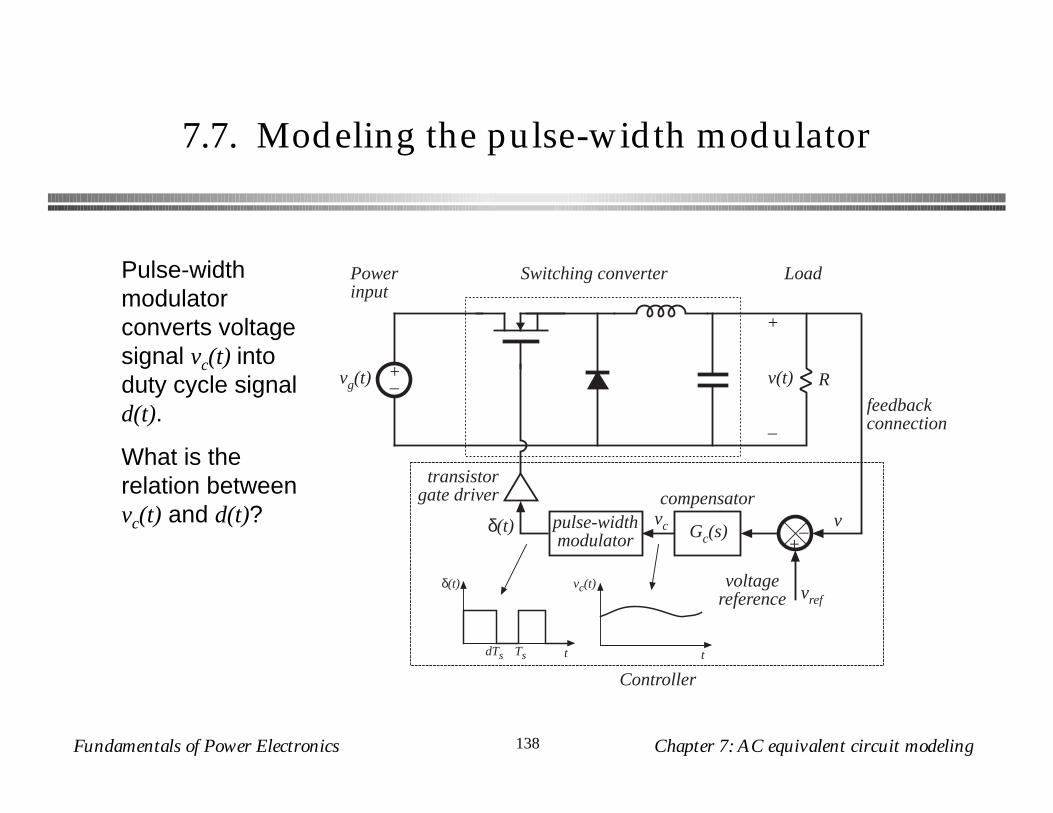
7.7. Modeling the pulse-width modulator
+–
+
v(t)
–
vg(t)
Switching converterPowerinput
Load–+
R
compensator
Gc(s)
vrefvoltage
reference
v
feedbackconnection
pulse-widthmodulator
vc
transistorgate driver
δ(t)
δ(t)
TsdTs t t
vc(t)
Controller
Pulse-width modulator converts voltage signal vc(t) into duty cycle signal d(t).
What is the relation between vc(t) and d(t)?
Fundamentals of Power Electronics Chapter 7: AC equivalent circuit modeling139
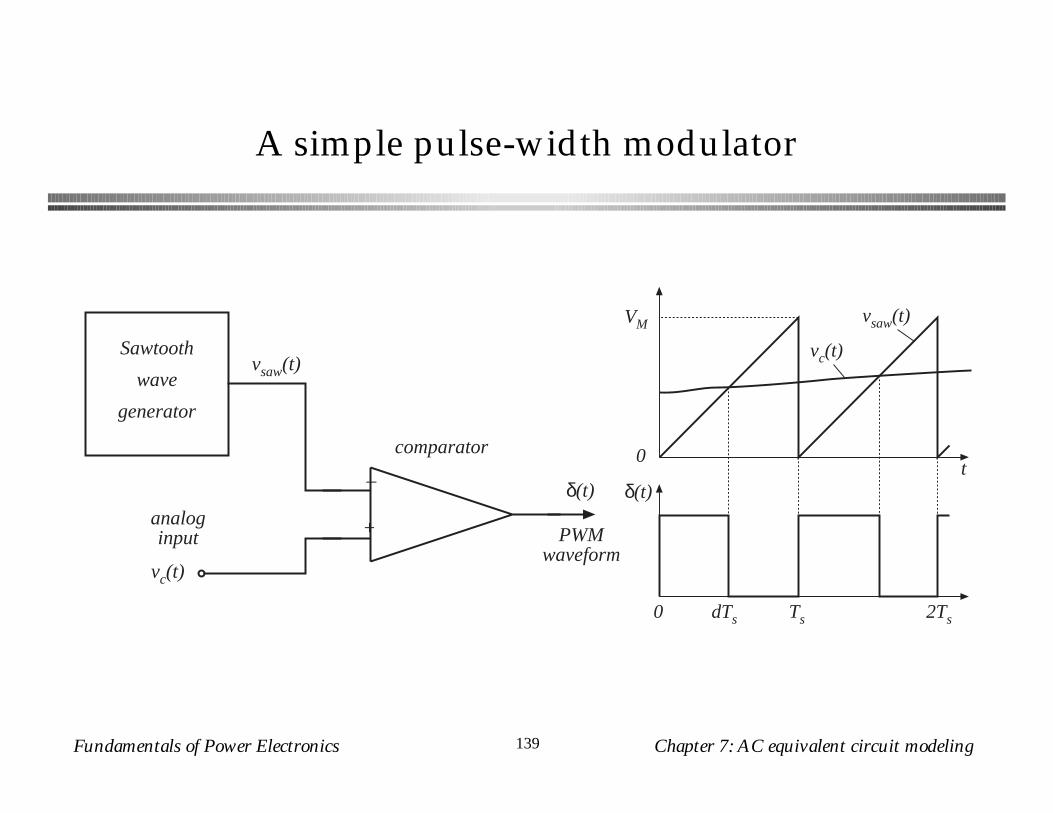
A simple pulse-width modulator
Sawtooth
wave
generator
+–
vsaw(t)
vc(t)
comparator
δ(t)
PWMwaveform
analoginput
vsaw(t)VM
0
δ(t)t
TsdTs
vc(t)
0 2Ts

Fundamentals of Power Electronics Chapter 7: AC equivalent circuit modeling140
Equation of pulse-width modulator
vsaw(t)VM
0
δ(t)t
TsdTs
vc(t)
0 2Ts
For a linear sawtooth waveform:
d(t) =vc(t)VM
for 0 ≤ vc(t) ≤ VM
So d(t) is a linear function of vc(t).

Fundamentals of Power Electronics Chapter 7: AC equivalent circuit modeling141
Perturbed equation of pulse-width modulator
vc(t) = Vc + vc(t)
d(t) = D + d(t)
d(t) =vc(t)VM
for 0 ≤ vc(t) ≤ VM
PWM equation:
Perturb:
D + d(t) =Vc + vc(t)
VM
Result:
D =Vc
VM
d(t) =vc(t)VM
pulse-widthmodulator
D + d(s)Vc + vc(s)1
VM
Block diagram:
Dc and ac relations:

Fundamentals of Power Electronics Chapter 7: AC equivalent circuit modeling142
Sampling in the pulse-width modulator
pulse-width modulator
1VM
vc dsampler
fs
The input voltage is a continuous function of time, but there can be only one discrete value of the duty cycle for each switching period.
Therefore, the pulse-width modulator samples the controlwaveform, with sampling rate equal to the switching frequency.
In practice, this limits the useful frequencies of ac variations to values much less than the switching frequency. Control system bandwidth must be sufficiently less than the Nyquist rate fs/2. Models that do not account for sampling are accurate only at frequencies much less than fs/2.
Fundamentals of Power Electronics Chapter 7: AC equivalent circuit modeling143
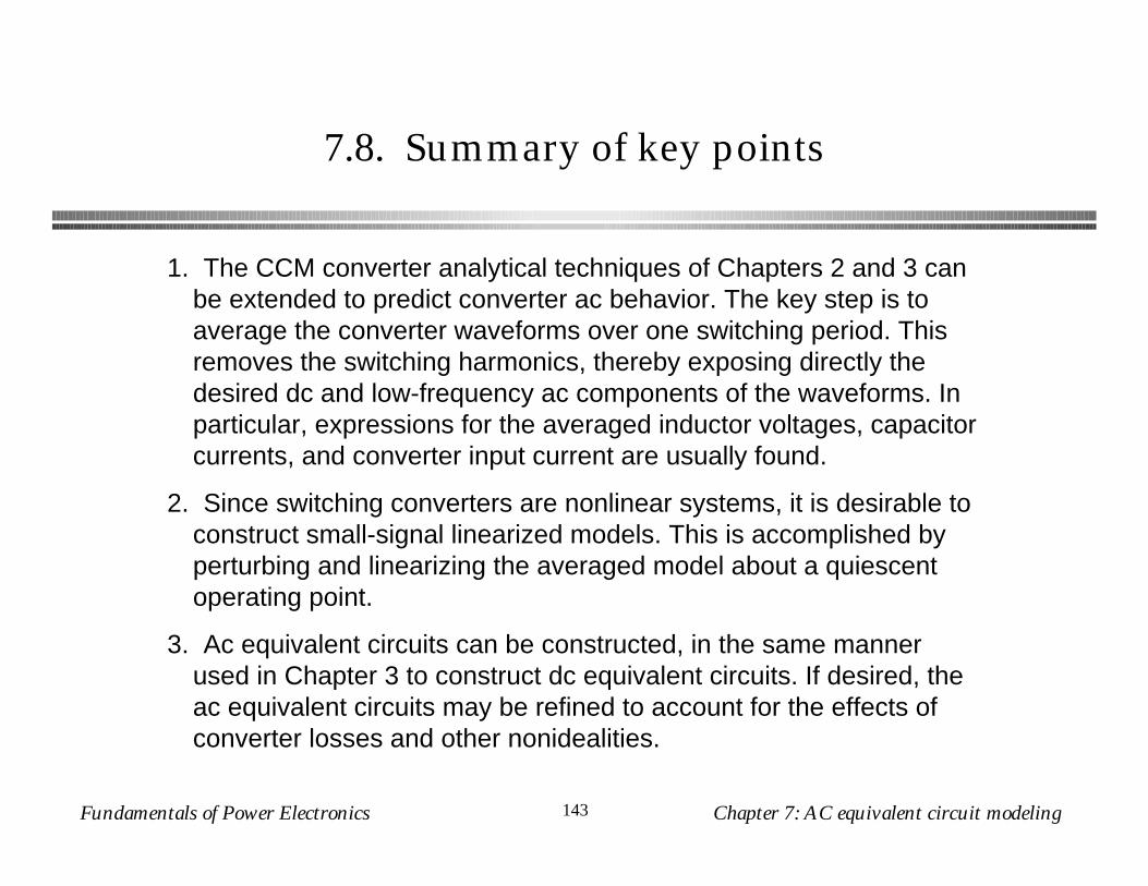
7.8. Summary of key points
1. The CCM converter analytical techniques of Chapters 2 and 3 can be extended to predict converter ac behavior. The key step is to average the converter waveforms over one switching period. This removes the switching harmonics, thereby exposing directly the desired dc and low-frequency ac components of the waveforms. In particular, expressions for the averaged inductor voltages, capacitor currents, and converter input current are usually found.
2. Since switching converters are nonlinear systems, it is desirable to construct small-signal linearized models. This is accomplished by perturbing and linearizing the averaged model about a quiescent operating point.
3. Ac equivalent circuits can be constructed, in the same manner used in Chapter 3 to construct dc equivalent circuits. If desired, the ac equivalent circuits may be refined to account for the effects of converter losses and other nonidealities.

Fundamentals of Power Electronics Chapter 7: AC equivalent circuit modeling144
Summary of key points
4. The state-space averaging method of section 7.4 is essentially the same as the basic approach of section 7.2, except that the formality of the state-space network description is used. The general results are listed in section 7.4.2.
5. The circuit averaging technique also yields equivalent results, but the derivation involves manipulation of circuits rather than equations. Switching elements are replaced by dependent voltage and current sources, whose waveforms are defined to be identical to the switch waveforms of the actual circuit. This leads to a circuit having a time-invariant topology. The waveforms are then averaged to remove the switching ripple, and perturbed and linearized about a quiescent operating point to obtain a small-signal model.

Fundamentals of Power Electronics Chapter 7: AC equivalent circuit modeling145
Summary of key points
6. When the switches are the only time-varying elements in the converter, then circuit averaging affects only the switch network. The converter model can then be derived by simply replacing the switch network with its averaged model. Dc and small-signal ac models of several common CCM switch networks are listed in section 7.5.4. Switching losses can also be modeled using this approach.
7. The canonical circuit describes the basic properties shared by all dc-dc PWM converters operating in the continuous conduction mode. At the heart of the model is the ideal 1:M(D) transformer, introduced in Chapter 3 to represent the basic dc-dc conversion function, and generalized here to include ac variations. The converter reactive elements introduce an effective low-pass filter into the network. The model also includes independent sources which represent the effect of duty cycle variations. The parameter values in the canonical models of several basic converters are tabulated for easy reference.
Fundamentals of Power Electronics Chapter 7: AC equivalent circuit modeling146
Summary of key points
8. The conventional pulse-width modulator circuit has linear gain, dependent on the slope of the sawtooth waveform, or equivalently on its peak-to-peak magnitude.