chapter 6 part - concordia universityrabinr/web_elec_312/past year... · created by: r. raut, ph.d....
TRANSCRIPT

Created by: R. Raut, Ph.D. Page 1 of 21 11/21/2012
Chapter 6
ELECTRONIC FILTERS, TUNED AMPLIFIERS and OSCILLATORS
6.1 Filter types, characteristics, parameters1 An electronic filter is a system which transmit signals in a specified frequency band to pass through with very little loss, while signals at some other frequency bands are severely attenuated through the system. An ideal low-pass filter will have a brick-wall type of transmission characteristics
Frequency
p
oK
Gain
0
Thus, the gain is constant over the frequency range 0 < w < wp and the gain abruptly reduces to zero at w = wp. The frequency range 0 wp is called the pass-band, the frequency wp is called the pass-band edge frequency. The band w > wp of frequencies is known as the stop- band. When the pass-band is 0 < w < wp and stop-band is w > wp, the filter is termed as a low- pass filter. Other types of filters are defined as follows. Passband Stopband Filter type wp < w < infinite 0 < w < wp High- pass wp1 < w < wp2 0 < w < wp1, wp2 < w < ∞ Band-pass 0 < w < wp1, wp2 < w < ∞ wp1 < w < wp2 Band -stop 0 < w < ∞ - All- pass An ideal characteristic such as the brick-wall type is seldom achievable in practice. Thus the ideal characteristic is approximated by suitable mathematical function. This is known as filter approximation problem. In this approximation, the loss in the pass-band is held
1 R. Raut and M.N.S. Swamy, Modern Analog Filter Analysis and Design, A Practical Approach , WILEY-VCH, ISBN 978-3-527-40766-8, © 2010.

Created by: R. Raut, Ph.D. Page 2 of 21 11/21/2012
to below an worst case limit Amax (or Ap), while the loss in the stop-band is held above an worst case minimum limit Amin (or Aa ). These losses are measured in decibels (db). The band of frequencies over which the loss changes gradually from Ap to Aa is known as the transition band. Narrower this transition band is, sharper is the gain characteristics of the filter and closer it is to ideal brick-wall characteristics. But more complex and expensive it becomes to realize such near ideal filters in practice. Before implementing a filter, one must know at least the following four parameters: Ap = Amax maximum loss (in decibels) in the pass- band Aa = Amin minimum loss (in decibels) in the stop-band wp = pass-band edge (i.e. frequency after which the loss becomes > Amax) wa = stop-band edge (frequency where the loss > Amin)
6.2 Transfer function, poles, zeros The filter transfer function is the ratio of an output quantity to an input quantity. Both of these will, in general, be functions of frequency. There can be four different kinds of transfer functions such as: Vo/Vi (voltage gain), Vo/Ii (trans-impedance gain), Io/Ii (current gain), and Io/Vi (trans-conductance gain) functions. In majority of the cases we shall assume the voltage gain function as the desired transfer function. Since these are functions of frequency one can readily write:
1 2
1 2
( ) ( )( )...( )( ) , , radian frequency.
( ) ( )( )...( )o M M
i N
V s a s z s z s zT s s j
V s s p s p s p
At the frequencies s = jw = z1, z2,….|T(s)| becomes = 0. So z1, z2…. are called transmission zeros. At the frequencies s = jw = p1, p2,….|T(s)| becomes = infinite. So p1, p2…. are called transmission poles or simply, the poles of the transfer function. If no transmission zeros are cited for finite values of the frequency w, it is assumed that the transmission zeros are located at infinity (i.e. for w infinity). When all the
Created by: R. Raut, Ph.D. Page 3 of 21 11/21/2012
transmission zeros are at infinity, the transfer function is known as an all- pole transfer function. Then
1 2
( )( ) , , radian frequency.
( ) ( )( )...( )o M
i N
V s aT s s j
V s s p s p s p
6.3 Maximally Flat, Butterworth and Chebyshev Filter functions Classically, it has been the practice to define a given filter response characteristics in terms of an associated low pass filter with a pass-band edge at wp =1 rad/sec. This reference filter is called the normalized low-pass filter. The actual filter transfer function can be obtained from this normalized low pass function by appropriately scaling the frequency variable ‘s’ or by transforming the frequency variable ‘s’ to other frequency function. For an all- pole filter function, two types of approximating functions are principally used to define the normalized low-pass function. These are:
1) Maximally flat magnitude approximation: In this function, the response is a continuous curve beginning at w = 0 and passes through a loss of Amax at w = wp. The functional form for a filter of order N (i.e., N number of poles) is:
2 2
1| ( ) |
1 ( ) N
p
T j
When = 1, the loss at w = wp is 120 log 3
1 1
(db). For this special case the
filter approximation is known as Butterworth approximation and the filter satisfying this characteristic is called a Butterworth filter. This is an all-pole filter function. In general, for maximally flat magnitude approximation
2 2 2max min20 log 1 , 20log 1 ( )a
p ap
A A A A
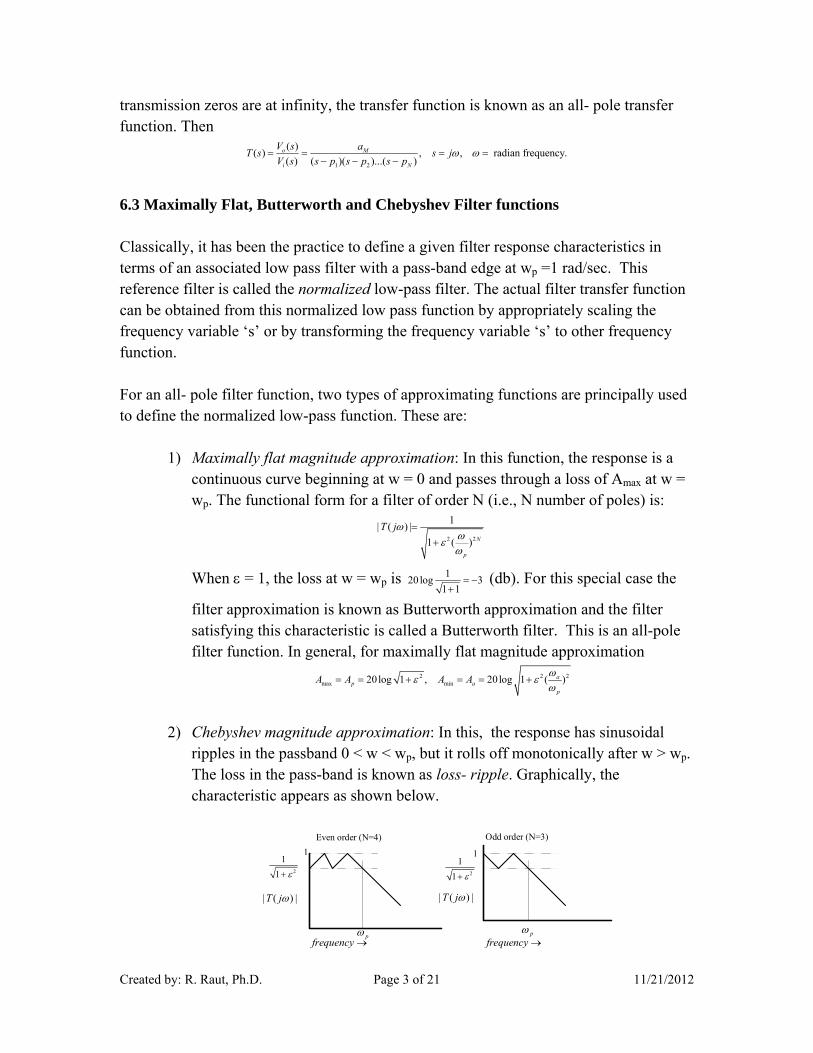
2) Chebyshev magnitude approximation: In this, the response has sinusoidal
ripples in the passband 0 < w < wp, but it rolls off monotonically after w > wp. The loss in the pass-band is known as loss- ripple. Graphically, the characteristic appears as shown below.
frequency frequency p p
| ( ) |T j | ( ) |T j
2
1
1 2
1
1
1 1
Even order (N=4) Odd order (N=3)

Created by: R. Raut, Ph.D. Page 4 of 21 11/21/2012
6.4 First order functions The order of the filter is represented by the degree of the denominator polynomial D(s) in the transfer function ( ) ( ) / ( )T s N s D s .Thus a first order transfer function can be given by
11 2
1
( ) , ( )o o
o o
A a s aT s T s
s b s
, and so on. The function T1(s) is an all-pole function with a gain
of Ao/wo at dc (i.e. w = 0), a pole at w = wo and represents a low -pass characteristic.The Second function T2(s) is a bilinear first order function since both the numerator N(s) and denominator D(s) have first order (i.e., exponent of ‘s’ is unity) terms in the complex frequency ‘s’. This function has a pole at 1/p o b , a zero at 1/z oa a , a low frequency (w
= 0, s = 0) gain of ao/wo and a high frequency (i.e., ) gain of a1/b1. Further reading suggestion (Sedra and Smith’s book, 5th edn. p.1098-1100, 6th edn. p. 1271-1273). A general second order transfer function is given by:
22 1
2 2( )
( / )o
o o
a s a s aT s
s Q s
Since both the numerator and denominator contain second order terms in ‘s’, this function is also known as a bi-qudratic (biquad) transfer function. The numerator function decide the type of the filter i.e., for a2, a1 = 0, T(s) becomes a low- pass filter. The denominator determines the pole frequency wo and the frequency selectivity (i.e., narrowness of the transition band of the filter) in terms of wo and Q. Q is called the pole-Q (pole quantity factor). The two poles of T(s) (i.e. zeros of D(s), D(s) = 0)) are given by:
21 2, / 2 1 1/ 4o op p Q j Q
A graphical plot reveals that for Q > 0.5, the poles become complex conjugate pair in the two dimensional (Re- and Im- axes) s-plane. This implies frequency selectivity. –wo/2Q is the real part of the poles. When Q is high, the real part becomes smaller, the poles become closer to the jw axis – this implies higher frequency selectivity.
2o
Q
21 1/ 4o Q
21 1/ 4o Q
S-planeleft-half right-half
Real-axis

Created by: R. Raut, Ph.D. Page 5 of 21 11/21/2012
Note that the real part of the poles is negative. If the real part becomes > 0 (i.e. equivalently Q < 0), the poles move to the right-half of the complex S- plane. This implies a response that grows with time ( from inverse Laplace transform on S, producing terms of the form te ) This represents an unstable system. In filter design this situation must be avoided. 6.5 Standard Biqudratic filter functions Seven possible types of second order filter can be defined for special values of the numerator coefficients. These are (i) Low-pass, (ii) High-pass, (iii) Band-pass, (iv) All-pass, (v) Low-pass notch, (vi) High-pass notch, and (vii) Notch filters. Further reading suggestion (Sedra and Smith’s book, 5th edn. p.1103-1105, 6th edn. 1276-1278). 6.5.1 Analysis of a typical second order filter network Consider the network below, which uses three operational amplifiers (as VCVS elements). Two of the OP-AMPs are connected as integrators and one as an inverting amplifier. This is known as Tow-Thomas filter network (after the inventor’s names) .
iV/R K
CC
R
R
r
r
QR
1oV
2oV3oV
#1OA
#2OA#3OA
The OA#2 is an integrator with only one input. We can readily write: 2 1 /o oV V sCR .
Similarly, for OA#3, 3 2 2o o o
rV V V
r . For OA#1, if one inspects carefully, it is possible to
figure out that this stage is functioning as an integrator with several inputs. These inputs are from Vi, Vo1, and V03. Then we can write:
1 1 3
1 1 1
( / )o i o oV V V VsC R K sCQR sCR

Created by: R. Raut, Ph.D. Page 6 of 21 11/21/2012
On substituting for Vo2 and Vo3, 1 1 1
1 1 1( )o i o o
KV V V V
sCR sCQR sCR sCR . Simplifying and changing
sides, we get: 1 2
1 1[1 ]
( )i
o
KVV
sCQR sCR sCR . On further simplification, we can get the voltage
transfer function 12 2 2 2
( ) ( / )/( )
( ) / (1/ ) ( / )o o
BPi o o
V s s Qs CRT s K H
V s s s QCR CR s s Q
.
The above represents a band-pass filter function. Thus, if we let s = jw, w 0, 1/CR and infinity successively, the magnitude | T(s) | becomes, respectively, zero, QK and zero. This response is that of a band pass filter. If we calculate Vo3 / Vi, it will show a low-pass filter characteristic. Design Example: Consider the design case for a second order band-pass filter with fo=1 kHz, Q=5. Use C in microfarads range. 6.6 Tuned Amplifiers Tuned amplifiers are amplifiers with a tuned circuit as its load. The tuned circuit is realized from a band-pass filter network. For high frequency application this is comprised of parallel LC elements.. The reason is that with small values (and hence small sizes) of L, C elements, the resonant frequency 1/o LC can be very high i.e., 100 KHz – 100
MHz. Further the tuned load circuit does not consume any DC power. The response of a tuned amplifier resembles a band-pass characteristic. The parallel L, C network imparts this band-pass filter characteristic. By virtue of amplification, one can achieve a band pass filtering function with enhancement of power in the desired signal frequency band. In studying tuned amplifiers, we shall assume that in the frequency range of tuning, the amplifying device (i.e. the BJT on MOS) is operating in the mind-band range. Thus the device ac equivalent circuit is purely resistive with a linear controlled source. Then, the voltage gain is given by the simple formula like –gm ZL where gm is the transconductance of the device and ZL is the impedance of the tuned circuit load. There are few special terms associated with a tuned amplifier. These are
a) Center frequency wo i.e. frequency at which gain vs. frequency curve shows maximum magnitude.
b) Bandwidth: B, the frequency values at which the gain is 3dB down relative to the gain at the center frequency. Quite often a selectivity factor is associated with a tuned amplifier response. This is designated by Q which is = wo /B .
Created by: R. Raut, Ph.D. Page 7 of 21 11/21/2012
c) Skirt selectivity: ratio of BW for -30 dB response to the BW for -3dB response relative to the response at wo, the center frequency
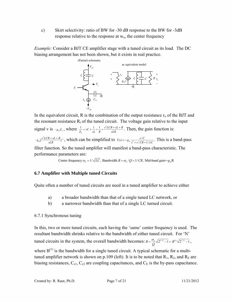
Example: Consider a BJT CE amplifier stage with a tuned circuit as its load. The DC biasing arrangement has not been shown, but it exists in real practice.
CCV
EEV
iVoV
ECEI
L CL C
_
v
mg v
rR
(Partial) schematicac equivalent model
ov
In the equivalent circuit, R is the combination of the output resistance ro of the BJT and the resonant resistance Rt of the tuned circuit. The voltage gain relative to the input
signal v is m Lg Z , where 21 1 1
L
s LCR sL RsC
Z sL R sLR
. Then, the gain function is:
21[ ]m
s LCR sL Rg
sLR
, which can be simplified to 2
/( )
/ 1/m
s CT s g
s s CR LC
. This is a band-pass
filter function. So the tuned amplifier will manifest a band-pass characteristic. The performance parameters are:
Center frequency 1/ , Bandwidth / 1/ , Mid-band gain=- R o o mLC B Q CR g
6.7 Amplifier with Multiple tuned Circuits Quite often a number of tuned circuits are need in a tuned amplifier to achieve either
a) a broader bandwidth than that of a single tuned LC network, or b) a narrower bandwidth than that of a single LC turned circuit.
6.7.1 Synchronous tuning In this, two or more tuned circuits, each having the ‘same’ center frequency is used. The resultant bandwidth shrinks relative to the bandwidth of either tuned circuit. For ‘N’
tuned circuits in the system, the overall bandwidth becomes: 1/ (1) 1/2 1 2 1N NoB BQ
,
where B(1) is the bandwidth for a single tuned circuit. A typical schematic for a multi-tuned amplifier network is shown on p.109 (left). It is to be noted that R1, R2, and RE are biasing resistances, Cc1, Cc2 are coupling capacitances, and CE is the by-pass capacitance.

Created by: R. Raut, Ph.D. Page 8 of 21 11/21/2012
The two LC networks have some resonant frequency, i.e.,1 1 2 2
1 1o
L C L C .
Example: Given fo = 10.7 MHz, two synchronous tuned stages. Overall 3 dB bandwidth is 200 kHz. L = 3µH. What will be C and R?
Use the relation 1/ (1) 1/2 1 2 1N NoB BQ
, with B200kHz, N=2, gives
B(1)310.83kHz. Since fo=10.7MHz, wo=2fo=1
LC. With L=3H, C=
2
1
oL=73.7pF.
Then, since the stage bandwidth (1) 1B
CR , and C=73.7pF. R=6.95 k.
6.7.2. Stagger Tuned System In this the two tuned circuits used have different center frequencies. As a result the overall response becomes more flat near the system center frequency. Consider the figure on p.113 (on left). Analysis shows that if ‘B’ is the system bandwidth and wo is the system center frequency, the center frequencies and BW of the constituent tuned circuit, for maximally flat band-pass response, are given by:
1 2 1 2 1 2, , , 22 2 2 2 2
oo o o o
B B BB B Q Q
B
These formulae are used to determine the design of the constituent band-pass tuned circuits. Examples: Sedra and Smith’s book, 5th edn. p.1148-1152 Exercises :D12.35, D12.36
Sedra and Smith’s book, 6th edn. p.1322-1327 Exercises :D16.35, D16.36 6.8 Sinusoidal Oscillators 6.8.1 Berkhausen Conditions for Oscillation In an oscillator an amplifier is connected with a feedback network in much the same way as in negative feedback system. But the difference is that now the feedback is positive. Thus, considering the feedback system diagram, one deduces, the feedback gain
s
of x
x
A
AA
1.
Considering frequency dependence of A and and letting
L(s) = A(s) (s), the loop gain, oscillation will occur when
L(s) = 0, i.e., Af infinite. Thus, A(s) (s) = 1 i.e. | A(jω)(jω) | = 1, and 0)]()(ATan[( jjA .
Created by: R. Raut, Ph.D. Page 9 of 21 11/21/2012
Thus when the magnitude of the loop gain is unity and phase of loop gain is 0 degrees with positive feedback, the system will oscillate i.e. xo will be finite although xs = 0. On putting s = jw, there can be only one frequency w = wo where the network will
simultaneously satisfy the two conditions . | A(s)(s) | = 1, and ( ) ( ) 0A s s . These
conditions are known as Berkhausen conditions. In this case, oscillation will occur at a single frequency wo and the wave shape will be sinusoidal. If the two conditions are not satisfied at a single frequency, there will be mixtures of frequencies in the oscillation and the oscillator wave form will be non-sinusoidal. It is convenient to assume that |A(jwo)| =
Am constant, so (wo) will determine the frequency of oscillation. 6.8.2: Oscillation Amplitude Control Attendant with the concept of infinite gain arises the question – will the amplitude of oscillation become infinite? It appears that the oscillation will grow beyond limits. But in reality no oscillator provides infinite output. The dilemma is solved by understanding that the concept of infinite gain arises under the assumption of a linear system with small signal input. As the signal level rises, the linearity assumption does not hold any more (why?, the transfer characteristic of a typical amplifier is non-linear). Thus, considering the devices that make up the amplifier, when signals are large, the operation goes into the non-linear region of the transfer characteristics. The result is a reduction in the gain
which thus tends to slow down the increase in |A| thereby limiting it to remain close to unity. Apart from the basic amplifier additional limiter circuit or certain voltage
dependent network element can be included in the feedback loop. This will facilitate |A| = 1 when the amplitude of the signal goes up. In any case, each practical system operates with finite valued power supplies and the oscillation amplitude can never exceed these values. If it tends to do so, distortions will set in and the oscillating waveform will no longer remain sinusoidal. 6.9 Active RC Oscillators (OP-AMP Based) 6.9.1. Wien-Bridge oscillator ( Sedra and Smith’s book, 5th edn., section 13.2, p.1171-1174; 6th edn., section 17.2, pp.1342-1344). Example: Sedra and Smith’s book, 5th edn. p.1174, Exercises :13.3
Sedra and Smith’s book, 6th edn. p.1344, Exercises :17.3
Note that the loop gain L(s) is: 2
1
, where 1p
p s
Z RK K
Z Z R
. For oscillation, Berkhausen
condition requires L(s)=1. That is KZp=Zp+Zs. Substituting for Zp and Zs, we get:

Created by: R. Raut, Ph.D. Page 10 of 21 11/21/2012
/( 1) 1/ .
1/
R sCK R sC
R sC
On simplifying, we get the quadratic equation
2 2 2 (2 1 ) 1 0s C R sRC K . The poles are the roots of the above equation, that is, 2 2 2 2 2
21 2 2 2
(3 ) (3 ) 4 3 1, (3 ) 4
2 2 2
RC K R C K R C Ks s K
R C RC RC
. With K=1+(20.3/10)=3.03
and RC=10k.16.10-9=16.10-5, one can get 5
1 2 5 5
.03 10, (0.015 )
32 10 16 10 16
js s j
.
(a) Frequency of oscillation 1o CR
, giving fo=994.718 Hz.
(b) At va node, the KCL is: 1 1 10.7 15 0.7 3.030.
3 1
v v v
K K
This gives v1=-3.36V.
Then vo=Kv1=3.03.(-3.36)V=-10.18 Volts. (c)
Demonstration by circuit simulation Figure WB Osc.1(a) shows the PSpice schematic for the oscillator with an OP-AMP set for a gain of +3. Since this satisfies the condition of oscillation, oscillatory signal is generated (Fig. WB Osc. (b)) but with only a small amplitude (i.e., 50 milli volts). This is because a gain of K=3 is just on the borderline of making the system unstable, i.e., oscillatory. In figure WB Osc.2(a), the OP-AMP is arranged to provide a non-inverting gain of +3.3. The growth of oscillation from a small value (~ noise floor level) to about the DC supply

Created by: R. Raut, Ph.D. Page 11 of 21 11/21/2012
WB Osc 1(a)
WB Osc. 1(b)

Created by: R. Raut, Ph.D. Page 12 of 21 11/21/2012
rail values of 10 V is visible (Fig. WB Osc.2(b)).
WB Osc. 2(a)
WB Osc. 2(b)

Created by: R. Raut, Ph.D. Page 13 of 21 11/21/2012
6.9.2. Phase Shift Oscillator (Sedra and Smith’s book, 5th edn., section 13.2.2, p.1174-1175) (Sedra and Smith’s book, 6th edn., section 17.2.2, p.1344-1346) The fundamental principle behind the operation of phase shift oscillator is the phase shift of 180o produced by several L-sections of R,C elements followed by an inverting gain amplifier (i.e., phase shift of 180o) which compensates for the attenuation produced in the signal by the chain of R,C elements. Thus the loop gain magnitude becomes unity while the total phase shift around the loop becomes 360o. Since a single L-section of R,C elements can produce a phase shift of at most 90o only when the frequency is infinite, while the infinite frequency is of no practical significance (it is just a mathematical concept), it is not possible to build any practical oscillator with two L-section of R,C elements, and an inverting amplifier. In practice, a minimum of three L-sections of R,C elements are employed to build the simplest possible oscillator. Figure PS Osc.1 shows this configuration, where a VCVS (i.e., a voltage amplifier) of gain –K is used to enable the total phase shift of 360o (equivalently zero degree) around the positive feedback loop.
C
R
C C
R R
Figure: PS Osc 1 Analysis using nodal admittance matrix (NAM): If we carefully review the results of analysis using NAM, it becomes clear that the transfer (i.e., gain) function for any of the nodal voltages (which are the objects of evaluation) has a denominator which is the determinant of the admittance matrix pertaining to the circuit on hand. For the same circuit, the denominator is fixed. From the principle of operation of an oscillator, which produces a signal without injection of any input signal (i.e., zero input signal), it is also understood that the voltage (or current) signal gain at any node of such system is infinity ,i.e., the denominator function in the gain expression as T(s)=N(s)/D(s) is zero.

Created by: R. Raut, Ph.D. Page 14 of 21 11/21/2012
The above observation provides a straightforward method to investigate the frequency of oscillation and the gain requirement in an oscillator by using the NAM analysis technique. The method involves (i) setting up the NAM, and then (ii)equate the determinant of the admittance matrix to zero. Since the determinant is a function of the complex variable s=jω, equating the real part and the imaginary part of the expression of the determinant to zero will lead to results related to the frequency of oscillation and the required gain of the amplifier to generate and sustain an oscillation. Considering Fig. PS Osc 1, the NAM equation can be written as (using a dummy source Ix at node 1, and G =1/R)
0
0
0
00
00
02
02
4
3
2
1 XI
V
V
V
V
sCsC
sCGsC
sCGsCsC
sCsCGsC
..PS Osc (1)
It is also understood that each row (say row#1) of the NAM equation represents the KCL at that node (i.e., node#1). Further the presence of the voltage amplifier forces a constraint equation between the input and output nodes of the amplifier. Thus, in case of Fig. PS Osc 1, we have V4 =-KV3. Incorporation of the constraint equation facilitates elimination of the dependent variable, which, in this case is the voltage at node 3 or at node 4. Using this information we can deduce an algorithm to re-write PS Osc (1) in a more compact form. The algorithm is (considering Yij as the admittance element in row i and column j) :
oldioldicurrenti YYY ||| 433 for al i=1,2,3,4 where KVV 34 / (in this case).
Further, since the KCL at the output node of a voltage amplifier (i.e., ideal VCVS) is arbitrary, the row associated with that node can be discarded from the NAM equation written in PS OSC (1). Hence, the reduced (in size) NAM equation becomes
0
0
0
2
2
3
2
1 XI
V
V
V
sCGsC
sCGsCsC
KsCsCGsC
..PS Osc (2)
The determinant of the matrix is
1),5(6 33332223 jKCCCGjCGG
Equating the real and imaginary parts to zero individually, we can get RC
o6
1 as
the frequency of oscillation, and K =29. This is the gain required of the inverting amplifier.

Created by: R. Raut, Ph.D. Page 15 of 21 11/21/2012
Demonstration by circuit simulation Figure PD Osc 1(a) shows the schematic of a phase shift oscillator where the inverting gain (of 30, i.e., actual gain -30) amplifier made from an OP-AMP is isolated from the
Figure: PS Osc 1(a) R,C network by an ideal unity gain buffer stage. This isolation is necessary for proper validation of the theoretical analysis. Figure PS Osc 1(b) shows the gradual growth of the oscillatory signal. Figure PS Osc 2(a) shows the circuit with an inverting gain of 33. Figure PS Osc 2(b) shows fully grown oscillation with amplitudes near the power supply values used for the OP-AMP.

Created by: R. Raut, Ph.D. Page 16 of 21 11/21/2012
Figure PS Osc 1(b)
Figure PS Osc 2(a):

Created by: R. Raut, Ph.D. Page 17 of 21 11/21/2012
Figure PS Osc 2(b):
6.10 LC Oscillators (Hartley and Colpitts Oscillator) (Sedra and Smith’s book, 5th edn., section 13.3, p.1179-1182) (Sedra and Smith’s book, 6th edn., section 17.3, p.1349-1353) Active R,C oscillators are efficient over a small range of frequencies (up to few kHz) especially because the active device (i.e., an OP-AMP) is severely limited in its high frequency response. At higher than few kHz, the parasitic capacitances of an OP-AMP can be included together with several resistances connected around the OP-AMP to build oscillators which are specifically known as active R oscillators. Oscillations in the range of few hundred kHz can be obtained from such systems, but the performance depends very much on the accuracy with which the internal characteristic of the OP-AMP is known to the designer. For oscillators with applications in MHz to few hundred MHz frequencies, the efficient choice is a pair of reactive elements (L, C – the inductance and the capacitor, together with a wide band amplifier. The wideband amplifier can be built from one or several transistor amplifier stages.

Created by: R. Raut, Ph.D. Page 18 of 21 11/21/2012
6.10.1 Colpitts Oscillators Colpitts oscillator is an L,C oscillator where the capacitor in the L,C tank circuit is split into two parts and the signal across one of the capacitors is fed back to compete the positive feedback loop. The active device is usually a single wide band transistor configured as a CE or CB BJT amplifier stage. Figures 1(a)-(b) show two possible configurations using respectively a CE and a CB BJT amplifier.
Figure Colpit Osc 1: Analysis using nodal admittance matrix: 6.10.1(a): Analysis for CE BJT-based Colpitts oscillator Consider the ac equivalent circuit, Fig. Colpit Osc 2, pertaining to the CE –Colpitts oscillator. The NAM (by inspection) equation is (with IX as a dummy source):
011
11
2
2
1
22
12
22
2VgI
V
V
gGsL
sCsL
sLsC
sLg
mXo
..Colpit Osc (1)
After re-arranging the dependent source gmV2, the NAM equation becomes
011
11
2
1
22
12
22
2 Xmo I
V
V
gGsL
sCsL
gsL
sCsL
g
..Colpit Osc (2)

Created by: R. Raut, Ph.D. Page 19 of 21 11/21/2012
Figure Colpit Osc 2: The determinant of the matrix is:
])([][ 21222222
222212
1222 moooo gggLCgLCGLCGgjCLCCCLggLGg In the above expression rgRGrg oo /1,/1,/1 22 . The real part of the expression is
][ 22212
1222 CLCCCLggLGg oo , while the imaginary part is
])([ 21222222
2 moo gggLCgLCGLCGg .
The determinant of the matrix has to be zero for oscillations to occur. Equating the real part to zero, we can get the frequency of oscillation as:
212
21222
CCL
CCgLgGLg ooo
, which is (approximately) =
212
21
CCL
CC , if we assume
go =0, i.e., ro = infinity.

Created by: R. Raut, Ph.D. Page 20 of 21 11/21/2012
Equating the imaginary part (i.e., coefficient of j) to zero and substituting ω=ωo will generate the design value of gm which will enable the oscillation to begin. On neglecting
go and gπ in comparison with gm, we can arrive at 12
2
CR
Cgm as a design equation
(approximate) for the oscillation. The detail is left as an exercise to the student. Note that gm is related to the DC bias current in the BJT device. 6.10.1(b): Analysis for CB BJT-based Colpitts oscillator Consider the ac equivalent circuit, Fig. Colpit Osc 3, pertaining to the CB –Colpitts oscillator. The NAM (by inspection) equation is (with IX as a dummy source):
Figure Colpit Osc 3:
vg
vgI
V
V
sLsCgsCg
sCgsCsCgGg
m
mX
oo
oo
2
1
488
8856
1 ..Colpit Osc (3)
Recognizing that 1Vv , and rearranging the dependent source gmV1, the NAM
equation becomes
Created by: R. Raut, Ph.D. Page 21 of 21 11/21/2012
01
2
1
488
8856X
omo
omo I
V
V
sLsCggsCg
sCggsCsCgGg ..Colpit Osc (4)
The determinant of the matrix is:
])([)[ 48454862
654852
8464 moooo gggLCgLCgLCGGjCLCCCLGgLgg In the above expression, rgRGrg oo /1,/1,/1 66 . The determinant of the matrix has
to be zero for oscillations to occur. The real part equated to zero gives the oscillation frequency
854
85464
CCL
CCLGgLgg ooo
, which approximates to (assuming go =0, i.e., ro =
infinity) 854
85
CCL
CCo
.
The imaginary part equated to zero leads to
0)( 48454862
6 moo gggLCgLCgLCGG . On substitution for ω=ωo,
neglecting go and gπ in comparison with gm, we can arrive at 56
8
CR
Cgm as a design
equation (approximate) for the oscillator. Note that gm is related to the DC bias current in the BJT device. 6.11: Crystal Oscillator (Reading suggestion: Sedra and Smith’s book, 5th edn., section 13.3.2, p.1182-1184) (Sedra and Smith’s book, 6th edn., section 17.3.2, p.1353-1355)