chapter 5 phase shifted carrier based pulse width...
TRANSCRIPT

103
CHAPTER 5
PHASE SHIFTED CARRIER BASED PULSE WIDTH
MODULATION
5.1 INTRODUCTION
In this chapter performance analysis of phase shifted carrier based
pulse width modulation techniques is presented. The reference voltage is
continuously compared with each of the shifted carrier signals. Each cell is
modulated independently using the PWM, which provides an even power
distribution among the cells. A carrier phase shift of 180°/m for the cascaded
inverter is introduced across the cells to generate a stepped multilevel output
waveform with lower distortion, where ‘m’ is the number of full bridge
inverters in a multilevel phase leg. The PSCPWM technique is divided into
two types, such as SH and SFO PWM techniques.
For n-level converter, (n-1) phase shifted carrier signals are
generated. The carriers between the full bridge inverters are phase shift
180º/m. If the reference is greater than carrier signal, then the active device
corresponding to that carrier is switched off.
The operating rules for PSC PWM when the number of level n = 5
are given below:
• The n – 1 = 4 carrier waveforms are arranged. The carriers
between the full bridge inverters are phase shifted 90º.

104
• The converter switches to + Vdc when the reference is greater
than all the carrier waveforms.
• The converter switches to Vdc / 2 when the reference is less
than the uppermost carrier waveform and greater than all
other carriers.
• The converter switches to 0 when the reference is less than
the two uppermost carrier waveform and greater than two
lowermost carriers.
• The converter switches to - Vdc / 2 when the reference is
greater than the lowermost carrier waveform and lesser than
all other carriers.
• The converter switches to -Vdc when the reference is lesser
than all the carrier waveforms.
5.2 SUBHARMONIC PWM
In SHPWM technique the reference voltage is continuously
compared with each of the shifted carrier signals. Figure 5.1 shows the
sinusoidal phase shifted pulse width modulation. Each cell is modulated
independently using sinusoidal unipolar pulse width modulation and bipolar
pulse width modulation respectively, which provides an even power
distribution among the cells. A carrier phase shift of 180°/m for cascaded
inverter is introduced across the cells to generate the stepped multilevel
output waveform with lower distortion.

105
Figure 5.1 PSC SHPWM
Phase shifting for carrier is given by,
n)1K(Pcr∏−
= (5.1)
Where, K is the Kth bridge.
n is the number of series connected single phase inverter.
21LN −
= (5.2)
Where, L is the number of switched DC levels that can be achieved
in each phase Leg.
The average output voltage for a phase shifted pulse width
modulation to a particular power cell ‘i’ is given by
106
∫= (t)dtVT1V oicr
oi (5.3)
dccr
onoi .V
TTV =
(5.4)
VVoi = (5.5)
Where, Voi is the output voltage of cell i, and Ton is the time
interval, determined by the comparison between the reference and the carrier
signals.
The phase shifted carrier SHPWM generator is shown in Figure 5.2.
The three phase sinusoidal modulating signals are generated by using phase
shift oscillator. This signal is compared with (n-1) phase shifted carrier waves
and PWM pulses are generated. These PWM pulses are applied to three phase
five level inverter.
The PSC SHPWM signal generation is shown in Figure 5.3.
• It is noted that when the sinusoidal reference signal is greater
than all carrier waves, +Vdc is obtained.
• When the sinusoidal reference signal is greater than carrier
wave except upper most carrier wave, +Vdc/2 is obtained.
• When the sinusoidal reference signal is greater than lower most
carrier and less than all carrier, –Vdc/2 is obtained.
• When the sinusoidal reference signal is lesser than all carrier
waves, –Vdc is obtained.

107
Figu
re 5
.2 S
imul
ink
diag
ram
ofP
SC S
HPW
M g
ener
atio
n

108
Figure 5.3 PSC SHPWM signal generation
5.2.1 Results
The simulation and hardware parameters for PSC SHPWM are as
follows:
• Three-phase load R = 100 Ohms & L = 20 mH
• Voltage level of each source Vdc = 100V
• Fundamental frequency = 50Hz
• Switching frequency = 5 kHz
The simulation and hardware output voltage for PSC SHPWM is
shown in Figures 5.4 and 5.5.

109
Figure 5.4 Simulation output voltage for PSC SHPWM
Figure 5.5 Hardware output voltage for PSC SHPWM
110
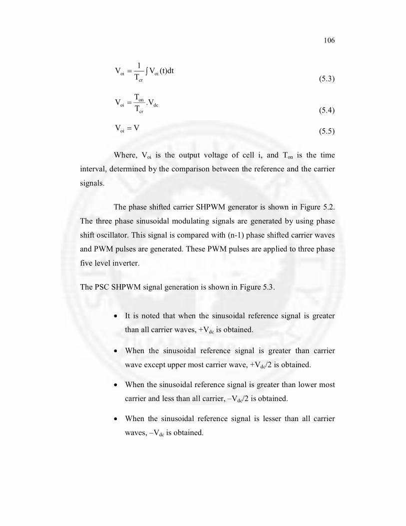
Figure 5.6 PSC SHPWM frequency spectrum
Figure 5.8 PSC SHPWM harmonic spectrum
The PSC SHPWM frequency spectrum is shown in Figure 5.6. In
frequency spectrum the switching frequency is 5 KHz with fundamental
frequency 50 Hz. The output voltage obtained by PSC SHPWM is about
212.9V for input voltage of 100V from each source. As switching frequency
is 5 KHz and fundamental frequency is 50Hz so harmonic order is about 100
which is shown in Figure 5.7. The THD value is about 3.84%.

111
5.3 SWITCHING FREQUENCY OPTIMAL PWM
This method takes the instantaneous average of the maximum and
minimum of the three reference voltages (Va, Vb, Vc) and subtracts the value
from each of the individual reference voltages to obtain the modulation
waveforms, which is shown in Figure 5.8.
Figure 5.8 PSC SFOPWM
From the above criteria we obtain the following equation.
⎭⎬⎫
⎩⎨⎧ +
=2
)V,V,Vmin()V,V,Vmax(V cbacbaoff
(5.6)
carrieraa VVSFOV −= (5.7)
carrierbb VVSFOV −= (5.8)
carriercc VVSFOV −= (5.9)

112
The carrier voltage is the average of maximum and minimum value
of Va,Vb,Vc. The phase voltage using SFO is the difference between reference
voltages to carrier voltage. The zero sequence modification made by the SFO
PWM technique restricts its use to three phase three wire system, however it
enables the modulation index to be increased by 15% before over modulation
or pulse dropping occurs.
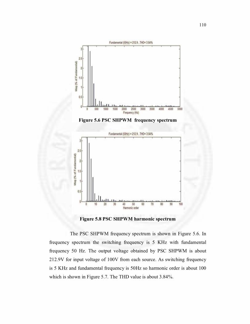
The phase shifted carrier SFOPWM generator is shown in
Figure 5.9. The three phase third harmonic modulating signals are generated.
This signal is compared with (n-1) phase shifted carrier waves and PWM
pulses are generated. These PWM pulses are applied to three phase five level
inverter.
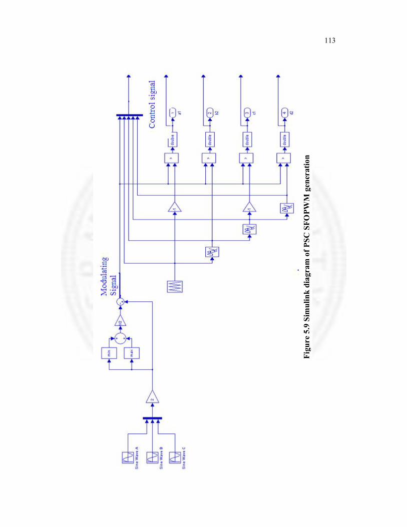
The PSC SFO-PDPWM signal generation is shown in Figure 5.10.
• It is noted that when the third harmonic reference signal is
greater than all carrier waves, +Vdc is obtained.
• When the third harmonic reference signal is greater than
carrier wave except upper most carrier wave, +Vdc/2 is
obtained.
• When the third harmonic reference signal is greater than
lower most carrier and less than all carrier, –Vdc/2 is obtained.
• When the third harmonic reference signal is lesser than all
carrier waves, –Vdc is obtained.
113
Figu
re 5
.9 S
imul
ink
diag
ram
ofP
SC S
FOPW
M g
ener
atio
n
114
Figure 5.10 Phase shifted carrier SFOPWM signal generation
5.3.1 Results
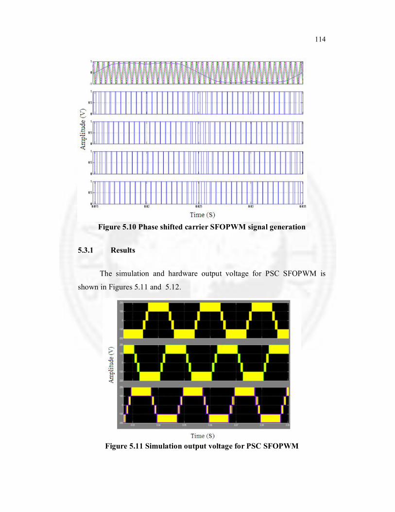
The simulation and hardware output voltage for PSC SFOPWM is
shown in Figures 5.11 and 5.12.
Figure 5.11 Simulation output voltage for PSC SFOPWM

115
Figure 5.12 Hardware output voltage for PSC SFOPWM
Figure 5.13 PSC SFOPWM frequency spectrum
Figure 5.13 PSC SFOPWM harmonic spectrum

116
The phase shifted carrier SFOPWM frequency spectrum is shown
in Figure 5.13. In frequency spectrum the switching frequency is 5000Hz with
fundamental frequency 50 Hz. The output voltage obtained by PSC
SFOPWM is about 220.2V for input voltage of 100V from each source. As
switching frequency is 5000Hz and fundamental frequency is 50Hz so
harmonic order is about 100 which is shown in Figure 5.14. The THD value is
about 20.65%.
The result confines that the output voltage in SH-PWM is 180.1V
and for SFO-PWM it is about 200V. It reveals, the THD for SH-PWM is
10.10% and for SFO-PWM it is 22.45%. From the above investigation, it
reveals that SH-PWM reduces THD and SFO-PWM enhances the output
voltage.
5.4 COMPARISON OF CSF, VSF AND PSC PWM
TECHNIQUES
The results of CSF, VSF and PSC PWM techniques using SH and
SFO methods are analyzed and THD as well as output voltage values are
compared as shown in Table 5.1, Figures 5.15 and 5.16.
The THD value and output voltage values are small in SH PWM
technique whereas the values are high in SFO PWM technique. It is observed
finally that with minimised THD, SH PWM method gives better results and
the SFO PWM technique is the most suitable in achieving the increased
output voltage.

117
Table 5.1 Output voltage and THD for CSF, VSF and PSC PWM
techniques
Figure 5.15 % of THD value for CSF, VSF and PSC PWM techniques

118
Figure 5.16 Output voltage for CSF, VSF and PSC PWM techniques
It is observed that the SH-PWM and SFO-PWM in PSC PWM
gives better result compared to the other methods. Here, the SH-PWM
strategy reduces the THD and SFO-PWM strategy enhances the output
voltage. The output voltage Vac is maintained between 180V to 200V. In CSF
SH-PWM, the THD value is 6.70% whereas in VSF PWM, it is 10.10% and
in PSC-PWM, it is about 3.84%. In CSF SFO-PWM the output voltage is
200V, THD value is 21.40% whereas it is about 22.45% in VSF PWM and in
PSC-PWM, output voltage is 220.2V and THD value is 20.65%.
5.5 HARDWARE DESCRIPTION
The Figure 5.17 shows the hardware setup for three phase cascaded
multilevel inverter. The hardware setup consists of six single phase inverter
sets using FSBB20CH60 Smart Power Module (SPM), six 100V DC power
supplies and Digital storage oscilloscope. The inverter topology is based on
the series connection of single phase inverters with separate DC sources. The
details of FSBB20CH60 SPM Data sheet is given in Appendix 1.

119
Figure 5.17 Experimental setup for three phase cascaded multilevel
inverter
The resulting phase voltage is synthesized by the addition of the
voltages generated by the different cells. In five level cascaded inverter each
single phase full-bridge inverter generates five voltages at the output side
+Vdc, +Vdc/2, 0, -Vdc/2, -Vdc. The staircase waveform is nearly sinusoidal, even
without filtering. The circuit is designed for a five-level inverter consisting of
12 IGBT switches. Each DC source connected with its respective H-bridge.
The experimental setup using hardware-cosimulation is shown in
Figure 5.18. The details of SPARTAN-3 FPGA Data sheet is given in
Appendix-2. System generator interfaces Xilinx/Spartan-3 device FPGA
hardware directly with simulink. The compilation target automatically
generates a bit stream file of the design and dumps it into FPGA-kit. The
system generator provides the FPGA SPARTAN-3 processor interface
through JTAG chain and USB. The JTAG options choose the boundary scan
position as 1 and detect the IR length such as 6 and 8. The platform USB

120
cable speed is 12 MHz. The compilation target automatically generates a bit
stream file and dumps it into FPGA kit. This hardware co-simulation system
clock frequency is set to 50 MHz at pin location C9. The FPGA board
generates 12-channel gate signals that drive the cascaded three phase
multilevel voltage source inverter IGBT switches [40-43].
A FPGA is made up of digital integrated circuits that can be
programmed to do any type of digital function. An FPGA has the ability to
operate faster [65]. FPGA consists of three major configurable elements.
There are
• Configurable Logic Blocks (CLB) arranged in an array that
provides the functional elements and implements most of the
logic in an FPGA.
• Input-Output Blocks (IOB) that provide the interface between
the package pins and the internal signal lines.
• Programmable interconnect resources that provide the routing
path to connect the inputs and outputs of the CLB and IOB onto
the appropriate network.
The VHDL program code is generated from the system generator
after the verification and simulation of the controller design. The VHDL
program is synthesized using Xilinx-ISE 9.1 software [24].

121
Figure 5.18 Experimental setup using hardware-co-simulation
The ISETM (Integrated Software Environment) based FPGA
design flow comprises the following steps:
1) Design entry
2) Design synthesis
3) Design implementation
4) Design verification
5) Xilinx® device programming.
122
The source code is written in the VHDL. After writing the code
syntax check has been performed on the code to verify whether code was
properly written using correct syntax [73-76].
The next step is HDL RTL simulation called behavioral simulation.
This step verifies whether the design entered is functionally correct or not.
For this simulation the VHDL test bench is written for PWM generator
architecture and simulation can be seen in Xilinx ISE simulator. If that is
functionally correct we have to move next step i.e., Synthesis.
The VHDL code of PWM generator is then synthesized using
Xilinx XST which is a part of Xilinx ISE software. The synthesis process has
been used for optimizing the design architecture selected. The resulting netlist
is saved to an NGC file. Then the synthesis report is generated which gives
information about how many logic blocks are used.
After the synthesis, the implementation is carried out. The
implementation part consists of three phases.
• Translate: Merge multiple design files into a single net list.
• Map: Group logical symbols from the net list (gates) into
physical components (Slices and IOBs).
• Place and route: Place components onto the chip, connect the
components, and extract timing data into reports.
Before translating the design, User Constrained File (UCF) is
written to assign the pin configuration of the FPGA to the PWM generator
I/Os. Once this is over, the translate merges together this UCF file and netlist
generated. Mapping is done to fit the design into the available resources of
target device i.e. FPGA. The last step of implementation is placing and

123
routing which places the logic blocks of the design into FPGA and route them
together. This operation produces NCD output file.
Figure 5.19 FPGA SPARTAN – 3 processor
In configuration, once a design is implemented, a file must be
created that the FPGA can understand. This file is called a bit stream or a BIT
file (.bit extension). The BIT file can be downloaded directly into the FPGA
via a serial interface or to an external memory device such as a Xilinx
platform flash PROM.
The XILINX/SPARTAN-3 FPGA processor is shown in
Figure 5.19. A FPGA controller board consists of 2 boards. One is FPGA
board and another one is peripheral interface board. FPGA board consists of
two SPARTAN-3 FPGA processors and peripheral board. The peripheral
board contains LCD, Micro switch and DAC. The function of FPGA
processor is to generate PWM signals and interfaced with power circuit. The

124
Xilinx device programming uses IMPACT to create a BIT file for debugging
and downloads it into the target device. Once the program is dumped to
FPGA kit, it acts as a PWM based FPGA controller and generates gate drive
switching pulses. These pulses are connected to optoisolator circuit for
preventing the ground sharing between the FPGA-processor and H-bridge
power module. The output of optoisolator is connected through driver to each
switching devices for controlling the PWM three phase cascaded multilevel
inverter.
Figure 5.20 shows the Spartan-3 processor, which includes the
following components and features:
1. 200,000-gate Xilinx Spartan-3 FPGA in a 256-ball thin ball
grid array package.
• 4,320 logic cell equivalents.
• Twelve 18K-bit block RAMs (216K bits).
• Twelve 18x18 hardware multipliers.
• Four Digital Clock Managers (DCMs).
• Up to 173 user-defined I/O signals.
2. 2Mbit Xilinx XCF02S Platform Flash, in-system
programmable configuration PROM.
• 1Mbit non-volatile data or application code storage
available after FPGA configuration.
3. Jumper options allow FPGA application to read PROM data
or FPGA configuration from other sources.
4. 1M-byte of Fast Asynchronous SRAM.
125
• Two 256Kx16 ISSI IS61LV25616AL-10T 10 ns
SRAMs.
• Configurable memory architecture.
• Single 256Kx32 SRAM array, ideal for MicroBlaze
code images.
• Two independent 256Kx16 SRAM arrays.
• Individual chip select per device.
• Individual byte enables.
5. 3-bit, 8-color VGA display port.
6. 9-pin RS-232 Serial Port.
• DB9 9-pin female connector (DCE connector).
7. RS-232 transceiver/level translator.
• Uses straight-through serial cable to connect to
computer or workstation serial port.
8. Second RS-232 transmit and receive channel available on
board test points.
9. PS/2-style mouse/keyboard port.
10. Four-character, seven-segment LED display.
11. Eight slide switches.
12. Eight individual LED outputs.
13. Four momentary-contact push button switches.
14. 50 MHz crystal oscillator clock source.

126
15. Socket for an auxiliary crystal oscillator clock source.
16. FPGA configuration mode selected via jumper settings.
17. Push button switch to force FPGA reconfiguration (FPGA
configuration happens automatically at power-on).
18. LED indicates when FPGA is successfully configured.
19. Three 40-pin expansion connection ports to extend and
enhance the Spartan-3 Board.
20. Three 40-pin expansion connection ports to extend and
enhance the Spartan-3 Board.
21. Three 40-pin expansion connection ports to extend and
enhance the Spartan-3 Board.
22. JTAG port.
23. Digilent JTAG download/debugging cable connects to PC
parallel port.
24. JTAG download/debug port compatible with the Xilinx
parallel cable IV and MultiPRO Desktop Tool.
25. AC power adapter input for included international
unregulated +5V power supply.
26. Power-on indicator LED.
27. On-board 3.3V regulator.
28. On-board 2.5V regulator.
29. On-board 1.2V regulator.

127
Figure 20 Xilinx Spartan – 3 processor block diagram

128
The function of Xilinx Spartan 3 FPGA processor-1 is to generate
PWM according to the needs. The PWM functions implemented in this FPGA
provides a broad range of functions and features. The PWM output from
FPGA-1 is terminated in a 34 pin connector through level translator for
converting 3.3V to 5V.
Translator is a device used in between FPGA I/O lines and FRC
header to translate 3.3V to 5V.
• Device used: SN74LVCC3245A
• Bi-directional voltage translator
• 2.3V to 3.6V on port A and 3V to 5.5V on port B
This 8 bit non-inverting bus transceiver contains two separate
supply rails. The port B is designed to track VCCB, which accepts voltages
from 3V to 5.5V and port A is designed to track VCCA, which operates at 2.3V
to 3.6V. This allows for translate from a 3.3V to 5V system environment.
The SN74LVCC32345 is designed for asynchronous
communication between data buses. The device transmits data from the A bus
to the B or from the B bus to the A bus, depending on the logic level at the
direction control input. The output-enable (OE) input can be used to disable
the device. The buses are effectively isolated. The 6 number translators are
used in FPGA board to convert 3.3V to 5V.
The output LEDs are used to verify the conditions or to debug the
code. The I/O lines from FPGA-1 are used to interface external peripherals.
To interface external peripheral devices, 26 I/O lines from FPGA-1 is
terminated in 26 pin header.

129
The FPGA-2 is mainly used to achieve the maximum throughput
rate of each SPI based ADCs. There are totally 4 ADCs interfaced with
FPGA. The AD7266 is a dual, 12 bit, high speed, low power, successive
approximation ADC that operates from a single 2.7V to 5.25V supply and
draws maximum current 6.2mA. This ADC uses advanced design techniques
to achieve very low power dissipation at 2MSPS throughput rate. FPGA-2
controls the functions of each ADC.
Peripheral device board contains the peripheral devices like DAC,
LCD & micro switches. This board is to interface with FPGA board through
26 pin header. The peripheral devices in the peripheral interface board are
controlled by the FPGA-1 in FPGA board.
The peripheral interface control board prominently features a 2 line
by 16 character liquid crystal display (LCD). The FPGA controls the LCD via
the 8 bit data interface pin. Once mastered, the LCD ia a practical way to
display a variety of information using standard ASCII. The AD5328 is octal
12 bit buffered voltage output DACs in a 16 lead TSSOP. They operate from
a single 2.5V to 5.5V supply, consuming 0.7mA at 3V. Their on-chip output
amplifiers allow the outputs to swing rail to rail with a slew rate of 0.7V/s.
The AD5328 use a versatile 3 wire serial interface that operates at clock rates
up to 30 MHz and is compatible with standard SPI, QSPI standards.

130
Figure 5.21 Hardware setup of five level cascaded inverter
The Figure 5.21 shows the hardware setup for three phase five level
cascaded inverter. The hardware setup consists of
• Six single phase inverter sets using FSBB20CH60 Smart
Power Module.
• Six numbers of high speed opto – isolator provided for PWM
isolation.
• One number of IGBT – SPM FSBB20CH60 with suitable
snubber circuit & heat sink provided for power circuit.
• Rating of device is 600V @ 20A
• One number of single phase diode rectifier (600V/25A) with
filter capacitor provided for input AC rectification for power
circuit input with fuse protection.

131
• Over current trip circuit provided for over load protection.
• One number of LED provided to indicate TRIP status.
• One number of RESET switch provided to reset the trip
function.
• Six numbers of banana connector termination provided in
power circuit input & external load interface.
• One number of 15 pin connector provided in control section
for waveform measurement in CRO.
It is an advanced smart power module (SPMTM) that Fairchild has
newly developed and designed to provide very compact. It combines
optimized circuit protection and drive matched to low loss IGBTs. System
reliability is further enhanced by the integrated under voltage lock-out and
short circuit protection. The high speed built-in HVIC provides optocoupler-
less single-supply IGBT gate driving capability that further reduce the overall
size of the inverter system design. Each phase current of inverter can be
monitored separately due to the divided negative dc terminals.
5.6 SUMMARY
The two proposed techniques namely SH and SFO are simulated
and performances analyzed by implementing FPGA SPARTAN-3 processor,
the results are obtained from experimental work which is almost similar to the
simulation work. Here, the SH-PWM strategy reduces the THD and SFO-
PWM strategy enhances the output voltage. The proposed controller design is
simulated and compilation portion is tested successfully through the FPGA
hardware in real time process.