chapter 4 the von neumann abstract discussion of …milom/cse240-fall05/handouts/ch04.pdf · von...
TRANSCRIPT

1
Chapter 4The Von NeumannModel
Based on slides © McGraw-HillAdditional material © 2004/2005 Lewis/Martin
4-2CSE 240
Warning!This is a bottom-up course
• No secrets, no magice.g., gates build on transistors, logic circuits from gates, etc.
But… This is a top-down lecture• You’ll have to trust me for a couple slides• Start with very abstract discussion of computer architecture• Meet with Chapter 3 material soon
4-3CSE 240
What Do We Know?A LOT!!
• Data representation (binary, 2’s complement, floating point, …)
• Transistors (p-type, n-type, CMOS)
• Gates (complementary logic)
• Combinational logic circuits (PLAs), memory (latches, flip-flops, …)
• Sequential logic circuits (state machines)
• Simple “processors” (programmable traffic sign)
What’s next?• Apply all this to traditional computing• Software interface: instructions• Hardware implementation: data path
4-4CSE 240
A Little Context1943: ENIAC
• First general electronic computer (Presper Eckert and John Mauchly)(Or was it Atananasoff in 1939? Or Konrad Zuse in 1941?)
• 18,000 tubes (had to replace 50 a day!)• Memory: 20 10-digit numbers (decimal)• Hard-wired program (via dials, switches,
and cables)• Completed in 1946
1944: Beginnings of EDVAC• Among other improvements, includes program stored in memory• Gave birth to UNIVAC-I (1951)• Completed in 1952
See Eniac by Scott McCartney

2
4-5CSE 240
Aside: Early MemoriesMercury delaylines!
Q’ Q1 0
M E
R C
U R
Y
Output
Input
Speaker
“Microphone”
4-6CSE 240
Context Continued: Stored Program Computer1945: John von Neumann
• First Draft of a Report on EDVAC
See John von Neumann and the Origins of Modern Computing by William Aspray
Von Neumann Machine (or Model)• Memory, containing instructions and data• Control unit, for interpreting instructions• Processing unit, for performing arithmetic and logical operations• Input/Output units, for interacting with real world
4-7CSE 240
Von Neumann ModelMEMORY
MAR MDR
INPUT Keyboard
MouseScanner
Disk
OUTPUT MonitorPrinterLEDDisk
PROCESSING UNIT
ALU TEMP
CONTROL UNIT
PC IR
4-8CSE 240
Memoryk x m array of stored bits (k is usually 2n)
Address• Unique (n-bit) identifier of location
Contents• m-bit value stored in location
Basic Operations• Load: read a value from a memory location• Store: write a value to a memory location
•••
0000000100100011010001010110
110111101111
00101101
10100010
3
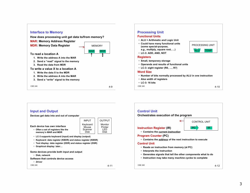
4-9CSE 240
Interface to MemoryHow does processing unit get data to/from memory?MAR: Memory Address RegisterMDR: Memory Data Register
To read a location A1. Write the address A into the MAR2. Send a “read” signal to the memory3. Read the data from MDR
To write a value X to a location A1. Write the data X to the MDR2. Write the address A into the MAR3. Send a “write” signal to the memory
MEMORY
MAR MDR
4-10CSE 240
Processing UnitFunctional Units• ALU = Arithmetic and Logic Unit• Could have many functional units
(some special-purpose,e.g., multiply, square root, …)
• LC-3: ADD, AND, NOTRegisters• Small, temporary storage• Operands and results of functional units• LC-3: eight register (R0, …, R7)
Word Size• Number of bits normally processed by ALU in one instruction• Also width of registers• LC-3: 16 bits
PROCESSING UNIT
ALU TEMP
4-11CSE 240
Input and OutputDevices get data into and out of computer
Each device has own interface• Often a set of registers like the
memory’s MAR and MDR
• LC-3 supports keyboard (input) and display (output)• Keyboard: data register (KBDR) and status register (KBSR)• Text display: data register (DDR) and status register (DSR)• Graphical display: later…
Some devices provide both input and output• Disk, network
Software that controls device access• Driver
INPUT Keyboard
MouseScanner
Disk
OUTPUT MonitorPrinterLEDDisk
4-12CSE 240
Control UnitOrchestrates execution of the program
Instruction Register (IR)• Contains the current instruction
Program Counter (PC)• Contains the address of the next instruction to execute
Control Unit• Reads an instruction from memory (at PC)• Interprets the instruction• Generates signals that tell the other components what to do• Instruction may take many machine cycles to complete
CONTROL UNIT
PC IR

4
4-13CSE 240
LC-3
4-14CSE 240
One More GateTri-state buffer
• NOT an inverter!
Allows wires to be “shared”• Alternative to mux• Only one source may drive at a time!
D Q
E
Z10Z00111001QDE
Z = “high impedance” state (no current, i.e., no “pressure”)
4-15CSE 240
InstructionsFundamental unit of workConstituents
• Opcode: operation to be performed• Operands: data/locations to be used for operation
Encoded as a sequence of bits (just like data!)• Sometimes have a fixed length (e.g., 16 or 32 bits)• Control unit interprets instruction
Generates control signals to carry out operation• Atomic: operation is either executed completely, or not at all
Instruction Set Architecture (ISA)• Computer’s instructions, their formats, their behaviors
4-16CSE 240
Example: LC-3 ADD InstructionLC-3 has 16-bit instructions
• Each instruction has a four-bit opcode, bits [15:12]LC-3 has eight registers (R0-R7) for temporary storage
• Sources and destination of ADD are registers
“Add the contents of R2 to the contents of R6,and store the result in R6.”

5
4-17CSE 240
Example: LC-3 LDR InstructionReads data from memoryBase + offset addressing mode
• Add offset to base register to produce memory address• Load from memory address into destination register
“Add the value 6 to the contents of R3 to form amemory address. Load the contents of memoryat that address and place the resulting data in R2.”
4-18CSE 240
Instruction ProcessingQuestion
• How are instructionsexecuted?
DECODE instruction
EVALUATE ADDRESS
FETCH OPERANDS
EXECUTE operation
STORE result
FETCH instruction from mem.
4-19CSE 240
Instruction Processing: FETCHIdea
• Put next instruction in IR & increment PC
Steps• Load contents of PC into MAR• Increment PC• Send “read” signal to memory• Read contents of MDR, store in IR
Who makes all this happen?• Control unit
EA
OP
EX
S
F
D
4-20CSE 240
FETCH in LC-3
Load PC into MDR (inc PC)Control
Data

6
4-21CSE 240
FETCH in LC-3
Load PC into MDRRead Memory
Control
Data
4-22CSE 240
FETCH in LC-3
Load PC into MDRRead MemoryCopy MDR into IR
Control
Data
4-23CSE 240
Instruction Processing: DECODEIdentify opcode
• In LC-3, always first four bits of instruction• 4-to-16 decoder asserts control line corresponding
to desired opcode
Identify operands from the remaining bits• Depends on opcode
e.g., for LDR, last six bits give offsete.g., for ADD, last three bits name source operand #2
Control unit implements DECODE
EA
OP
EX
S
F
D
4-24CSE 240
DECODE in LC-3

7
4-25CSE 240
Instruction Processing: EVALUATE ADDRESSCompute address
• For loads and stores• For control-flow instructions (more later)
Examples• Add offset to base register (as in LDR)• Add offset to PC (as in LD and BR)
EA
OP
EX
S
F
D
4-26CSE 240
EVALUATE ADDRESS in LC-3
Load/Store
4-27CSE 240
Instruction Processing: FETCH OPERANDSGet source operands for operation
Examples• Read data from register file (ADD)• Load data from memory (LDR)
EA
OP
EX
S
F
D
4-28CSE 240
FETCH OPERANDS in LC-3
ADD

8
4-29CSE 240
FETCH OPERANDS in LC-3
LDR
4-30CSE 240
Instruction Processing: EXECUTEActually perform operation
Examples• Send operands to ALU and assert ADD signal• Do nothing (e.g., for loads and stores)
EA
OP
EX
S
F
D
4-31CSE 240
EXECUTE in LC-3
ADD
4-32CSE 240
Instruction Processing: STOREWrite results to destination
• Register or memory
Examples• Result of ADD is placed in destination reg.• Result of load instruction placed in destination reg.• For store instruction, place data in memory
Set MDRAssert WRITE signal to memory
EA
OP
EX
S
F
D

9
4-33CSE 240
STORE in LC-3
ADD
4-34CSE 240
STORE in LC-3
LDR
4-35CSE 240
STORE in LC-3
STORESet MDR
4-36CSE 240
STORE in LC-3
STORESet MDRAssert “write”

10
4-37CSE 240
Changing the Sequence of InstructionsRecall FETCH
• Increment PC by 1
What if we don’t want linear execution?• E.g., loop, if-then, function call
Need instructions that change PC• Jumps are unconditional
Always change the PC• Branches are conditional
Change the PC only if some condition is truee.g., the contents of a register is zero
4-38CSE 240
Example: LC-3 JMP InstructionSet the PC to the value of a register
• Fetch next instruction from this address
“Load the contents of register R3 into the PC.”
0 0 0 0 0 0
0 0 0 0 0 0
4-39CSE 240
How Does Control Unit Work?
4-40CSE 240
Remember Finite State Machines?
State Machine
CombinationalLogic Circuit
StorageElements
Inputs Outputs
State
Next state
Cur
rent
sta
tePC,IR Control signals

11
4-41CSE 240
Control Unit DetailsFinite state machine
• Input: PC, IR• Output: many control signals
Need to map abstract opsto control signals
• E.g., MAR <- PC ⇒ GatePC and LD.MAR
• E.g., PC <- PC + 1 ⇒ PCMUX=2 and LD.PC
LC-3• 35 states (Fig. C.2)
4-42CSE 240
Instruction Processing SummaryInstructions look just like data
• Interpreted by machine (or software)
Three basic kinds of instructions• Computational instructions (ADD, AND, …)• Data movement instructions (LD, ST, …)• Control instructions (JMP, BRnz, …)
Six basic phases of instruction processing
F → D → EA → OP → EX → S• Not all phases are needed by every instruction• Multiple phases per cycle possible• Phases may take variable number of machine cycles
4-43CSE 240
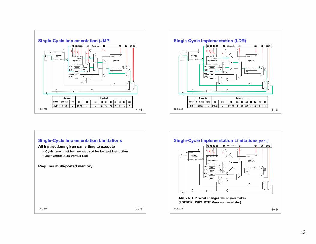
Alternate Implementation
Execute Each Instruction in Single Cycle• Much simpler• All phases happen in one cycle
4-44CSE 240
Single-Cycle Implementation (ADD)
101000001I[11:9]I[2:0]I[8:6]00001ADD
I[5]I[15:12]InstrControlOpcode
12
4-45CSE 240
Single-Cycle Implementation (JMP)
0x1000100--I[8:6]-1100JMP
I[5]I[15:12]InstrControlOpcode
4-46CSE 240
Single-Cycle Implementation (LDR)
100000101I[11:9]-I[8:6]-0110LDR
I[5]I[15:12]InstrControlOpcode
4-47CSE 240
Single-Cycle Implementation LimitationsAll instructions given same time to execute
• Cycle time must be time required for longest instruction• JMP versus ADD versus LDR
Requires multi-ported memory
4-48CSE 240
Single-Cycle Implementation Limitations (cont.)
AND? NOT? What changes would you make?(LDI/STI? JSR? RTI? More on these later)
13
4-49CSE 240
Next TimeLecture
• LC-3
Reading• Chapter 5 - 5.2
Quiz• Online!
Upcoming• Homework due Monday 11 October