chapter 4 the processor · chapter 4 the processor 4.1 introduction 244 ... o the alu is an example...
TRANSCRIPT

CMPS290 Class Notes (Chap04) Page 1 / 33 by Kuo-pao Yang
CHAPTER 4
The Processor
4.1 Introduction 244
4.2 Logic Design Conventions 248
4.3 Building a Datapath 251
4.4 A Simple Implementation Scheme 259
4.5 An Overview of Pipelining 272
4.6 Pipelined Datapath and Control 286
4.7 Data Hazards: Forwarding versus Stalling 303
4.8 Control Hazards 316
4.9 Exceptions 325
4.10 Parallelism via Instructions 332
4.11 Real Stuff: The ARM Cortex-A8 and Intel Core i7 Pipelines 344
4.12 Going Faster: Instruction-Level Parallelism and Matrix Multiply
351
4.13 Advanced Topic: an Introduction to Digital Design Using a
Hardware Design Language to Describe and Model a Pipeline and
More Pipelining Illustrations 354
4.14 Fallacies and Pitfalls 355
4.15 Concluding Remarks 356
4.16 Historical Perspective and Further Reading 357
4.17 Exercises 357

CMPS290 Class Notes (Chap04) Page 2 / 33 by Kuo-pao Yang
4.1 Introduction 244
The performance of a computer is determined by three key factors: instruction count,
clock cycle time, and clock cycles per instruction (CPI).
o Instruction count: Determined by compiler and the instruction set architecture
(ISA)
o Clock cycle time and CPI: Determined by the implementation of the processor,
CPU hardware
We will examine two different implementations of the MIPS instruction set
o A simplified version
o A more realistic pipelined version
A Basic MIPS implementation We will be examining an implementation that includes a subset of the core MIPS
instruction set:
o Memory-reference instructions: load word (lw) and store word (sw)
o Arithmetic-logical instructions: add, sub, AND, OR, and slt
o Branch instructions: bracnh equal (beq) and jump (j)
CMPS290 Class Notes (Chap04) Page 3 / 33 by Kuo-pao Yang
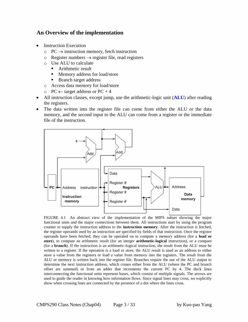
An Overview of the implementation
Instruction Execution
o PC instruction memory, fetch instruction
o Register numbers register file, read registers
o Use ALU to calculate
Arithmetic result
Memory address for load/store
Branch target address
o Access data memory for load/store
o PC target address or PC + 4
All instruction classes, except jump, use the arithmetic-logic unit (ALU) after reading
the registers.
The data written into the register file can come from either the ALU or the data
memory, and the second input to the ALU can come from a register or the immediate
file of the instruction.
FIGURE 4.1 An abstract view of the implementation of the MIPS subset showing the major
functional units and the major connections between them. All instructions start by using the program
counter to supply the instruction address to the instruction memory. After the instruction is fetched,
the register operands used by an instruction are specified by fields of that instruction. Once the register
operands have been fetched, they can be operated on to compute a memory address (for a load or
store), to compute an arithmetic result (for an integer arithmetic-logical instruction), or a compare
(for a branch). If the instruction is an arithmetic-logical instruction, the result from the ALU must be
written to a register. If the operation is a load or store, the ALU result is used as an address to either
store a value from the registers or load a value from memory into the registers. The result from the
ALU or memory is written back into the register file. Branches require the use of the ALU output to
determine the next instruction address, which comes either from the ALU (where the PC and branch
offset are summed) or from an adder that increments the current PC by 4. The thick lines
interconnecting the functional units represent buses, which consist of multiple signals. The arrows are
used to guide the reader in knowing how information flows. Since signal lines may cross, we explicitly
show when crossing lines are connected by the presence of a dot where the lines cross.

CMPS290 Class Notes (Chap04) Page 4 / 33 by Kuo-pao Yang
In practice, these data lines cannot simply be wired together; we must add a logic
element that choose from among the multiple sources and steers one of those source
to its destination. This selection is commonly done with a device call a multiplexor,
although this device might better be called a data selector.
The ALU must perform one of several operations. (Appendix B describes the
detailed design of the ALU) Like the multiplexors, control lines that are set on the
basis of various filed in the instruction direct these operations.
Figure 4.2 show the datapath of Figure 4.1 with the three required multiplexors
added, as well as control lines for the major function units.
A control unit which has the instruction as an input, is used to determine how to set
the control lines for the functional units and two of the multiplexors.
The third multiplexors which determined whether PC + 4 or the branch destination
address is written into the PC, is set based on the Zero output of the ALU, which is
used to perform the comparison of a beq instruction.
FIGURE 4.2 The basic implementation of the MIPS subset, including the necessary multiplexors
and control lines. The top multiplexor (“Mux”) controls what value replaces the PC (PC + 4 or the
branch destination address); the multiplexor is controlled by the gate that “ANDs” together the Zero
output of the ALU and a control signal that indicates that the instruction is a branch. The middle
multiplexor, whose output returns to the register file, is used to steer the output of the ALU (in the case
of an arithmetic-logical instruction) or the output of the data memory (in the case of a load) for writing
into the register file. Finally, the bottommost multiplexor is used to determine whether the second
ALU input is from the registers (for an arithmetic-logical instruction or a branch) or from the offset
field of the instruction (for a load or store). The added control lines are straightforward and determine
the operation performed at the ALU, whether the data memory should read or write, and whether the
registers should perform a write operation. The control lines are shown in color to make them easier to
see.

CMPS290 Class Notes (Chap04) Page 5 / 33 by Kuo-pao Yang
4.2 Logic Design Conventions 248
The datapath elements in the MIPS implementation consist of two different types of
logic elements: elements that operate on data values (combinational elements) and
elements that contain state (state elements)
Combinational elements:
o Their outputs depend only on the current input.
o The ALU is an example of combinational element.
o Given the same input, a combinational element always produces the same output
because it has no internal storage.
State elements:
o An element contains state if it has some internal storage.
o In Figure 4.1, the instruction and data memories, as well as the registers, are all
examples of state elements.
o A state element has at least two inputs and one output. The required inputs are the
data value to be written into the element and the clock.
o The clock is used to determine when the state element should be written: a state
element can be read at any time.
o Logic components that contain state are also called sequential because their
outputs depend on both their input and the contents of the internal state.

CMPS290 Class Notes (Chap04) Page 6 / 33 by Kuo-pao Yang
Clocking Methodology
A clocking methodology defines when signals can be read and when they can be
written.
We will assume an edge-triggered clocking methodology. An edge-triggered clocking
methodology means that any values stored in a sequential logic element are updated
only on a clock edge.
Figure 4.3 shows the two state elements surrounding a block of combinational logic,
which operates in a single clock cycle: all signals must propagate from state element
1, through the combinational logic and to state element 2 in the time of one clock
cycle.
The state element is changed only when the write control signal is asserted and a
clock edge occurs.
We will use the word asserted to indicate a signal that is logically high and assert to
specify that a signal should be driven logically high, and deassert or deasserted to
represent logically low.
FIGURE 4.3 Combinational logic, state elements, and the clock are closely related. In a synchronous
digital system, the clock determines when elements with state will write values into internal storage.
Any inputs to a state element must reach a stable value (that is, have reached a value from which they
will not change until after the clock edge) before the active clock edge causes the state to be updated.
All state elements in this chapter, including memory, are assumed to be positive edge-triggered; that is,
they change on the rising clock edge.
Figure 4.4 gives a generic example. All writes take place on the rising clock edge
(from low to high) or on the falling clock edge (from high to low), since the input to
the combinational logic block cannot change except on the chosen clock edge. In this
book we sue the rising clock edge.
FIGURE 4.4 An edge-triggered methodology allows a state element to be read and written in the
same clock cycle without creating a race that could lead to indeterminate data values. Of course, the
clock cycle still must be long enough so that the input values are stable when the active clock edge
occurs. Feedback cannot occur within one clock cycle because of the edge-triggered update of the state
element. If feedback were possible, this design could not work properly. Our designs in this chapter
and the next rely on the edge-triggered timing methodology and on structures like the one shown in
this figure.

CMPS290 Class Notes (Chap04) Page 7 / 33 by Kuo-pao Yang
4.3 Building a Datapath 251
Instruction Fetch:
o Instruction memory: a memory unit to store instruction of a program and supply
instruction given an address.
o Program counter (PC): a register that hold the address of the current instruction.
o Adder: an adder to increment the PC to the address of the next instruction.
Figure 4.6 show how to combine the three elements to form a datapath that fetches
instructions and increments the PC to obtain the address of the next sequential
instruction.
FIGURE 4.6 A portion of the datapath used for fetching instructions and incrementing the program
counter. The fetched instruction is used by other parts of the datapath.

CMPS290 Class Notes (Chap04) Page 8 / 33 by Kuo-pao Yang
R-type Instructions
R-format instructions all read two registers, perform an ALU operation on the
contents of the register, and write the result to a register.
We call these instructions either R-type instructions or arithmetic-logical instructions.
This instruction class includes add, sub, AND, OR, and slt.
Recall that a typical instance of such an instruction is:
add $t1, $t2, $t3 # $t1 = $t2 + $t3
R-format Instructions:
o Read two register operands
o Perform arithmetic/logical operation
o Write register result
Register file:
o The processor’s 32 general-purpose registers are stored in a structure called a
register file.
o A register file is a collection of registers in which any register can be read or
written by specifying the number of the register in the file.
o The register file always outputs the contents of whatever register number are on
the Read register inputs.
o To write a data word, we will need two inputs: one to specify the register number
to be written and one to supply the data to be written into the register. Writes are
controlled by the write control signal (RegWrite), which must be asserted for a
write to occur at the clock edge.
Figure 4.7a show the result; we need a total of four inputs (three for register numbers
and one for data) and two outputs (both for data). The register number inputs are 5
bits wide to specify one of 32 registers (32 = 25), whereas the data input and two data
output buses are each 32 bits wide.
Figure 4.7b shows the ALU, which takes two 32-bit inputs and produces a 32-bit
result, and well as a 1-bit signal Zero if the result is 0. The 4-bit control of the ALU
signal (ALU operation) is described in detail in Appendix B; we will review the
ALU control shortly.
FIGURE 4.7 The two elements needed to implement R-format ALU operations are the register file
and the ALU. The register file contains all the registers and has two read ports and one write port. The

CMPS290 Class Notes (Chap04) Page 9 / 33 by Kuo-pao Yang
design of multiported register files is discussed in Section B.8 of Appendix B. The register file
always outputs the contents of the registers corresponding to the Read register inputs on the outputs; no
other control inputs are needed. In contrast, a register write must be explicitly indicated by asserting
the write control signal. Remember that writes are edge-triggered, so that all the write inputs (i.e., the
value to be written, the register number, and the write control signal) must be valid at the clock edge.
Since writes to the register file are edge-triggered, our design can legally read and write the same
register within a clock cycle: the read will get the value written in an earlier clock cycle, while the
value written will be available to a read in a subsequent clock cycle. The inputs carrying the register
number to the register file are all 5 bits wide, whereas the lines carrying data values are 32 bits wide.
The operation to be performed by the ALU is controlled with the ALU operation signal, which will be
4 bits wide, using the ALU designed in Appendix B. We will use the Zero detection output of the
ALU shortly to implement branches. The overflow output will not be needed until Section 4.9, when
we discuss exceptions; we omit it until then.

CMPS290 Class Notes (Chap04) Page 10 / 33 by Kuo-pao Yang
Load/Store Instructions
Next, consider the MIPS load word (lw) and store word (sw) instructions, which have
the general form:
lw $t1, offset ($t2) # $t1 = Memory [$t2 + offset]
sw $t1, offset ($t2) # Memory [$t2 + offset] = $t1
Load/Store Instructions:
o Read register operands
o Calculate address using 16-bit offset
Use ALU, but sign-extend offset
o Load: Read memory and update register
o Store: Write register value to memory
FIGURE 4.8 The two units needed to implement loads and stores, in addition to the register file and
ALU of Figure 4.7, are the data memory unit and the sign extension unit. The memory unit is a state
element with inputs for the address and the write data, and a single output for the read result. There are
separate read and write controls, although only one of these may be asserted on any given clock. The
memory unit needs a read signal, since, unlike the register file, reading the value of an invalid address
can cause problems, as we will see in Chapter 5. The sign extension unit has a 16-bit input that is sign-
extended into a 32-bit result appearing on the output (see Chapter 2). We assume the data memory is
edge-triggered for writes. Standard memory chips actually have a write enable signal that is used for
writes. Although the write enable is not edge-triggered, our edge-triggered design could easily be
adapted to work with real memory chips. See Section B.8 of Appendix B for further discussion of how
real memory chips work.

CMPS290 Class Notes (Chap04) Page 11 / 33 by Kuo-pao Yang
Branch-on-Equal Instruction
The beq branch instruction has three operands, two register that are compared for
equality, and a 16-bit offset used to compute the branch target address relative to the
branch instruction address.
beq $t1, $t2, offset # if ($t1 == $t2) go to (PC + 4) + (offset * 4)
Branch Instruction
o Read register operands
o Compare operands
Use ALU, subtract and check Zero output
o Calculate target address
Sign-extend displacement
Shift left 2 places (word displacement)
Add to PC + 4: Already calculated by instruction fetch
FIGURE 4.9 The datapath for a branch uses the ALU to evaluate the branch condition and a separate
adder to compute the branch target as the sum of the incremented PC and the sign-extended, lower 16
bits of the instruction (the branch displacement), shifted left 2 bits. The unit labeled Shift left 2 is
simply a routing of the signals between input and output that adds 00two to the low-order end of the
sign-extended offset field; no actual shift hardware is needed, since the amount of the “shift” is
constant. Since we know that the offset was sign-extended from 16 bits, the shift will throw away only
“sign bits.” Control logic is used to decide whether the incremented PC or branch target should replace
the PC, based on the Zero output of the ALU.
CMPS290 Class Notes (Chap04) Page 12 / 33 by Kuo-pao Yang
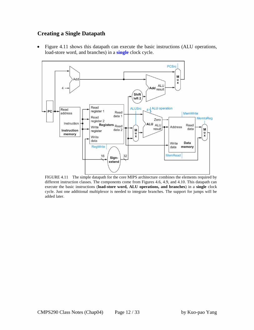
Creating a Single Datapath
Figure 4.11 shows this datapath can execute the basic instructions (ALU operations,
load-store word, and branches) in a single clock cycle.
FIGURE 4.11 The simple datapath for the core MIPS architecture combines the elements required by
different instruction classes. The components come from Figures 4.6, 4.9, and 4.10. This datapath can
execute the basic instructions (load-store word, ALU operations, and branches) in a single clock
cycle. Just one additional multiplexor is needed to integrate branches. The support for jumps will be
added later.
CMPS290 Class Notes (Chap04) Page 13 / 33 by Kuo-pao Yang
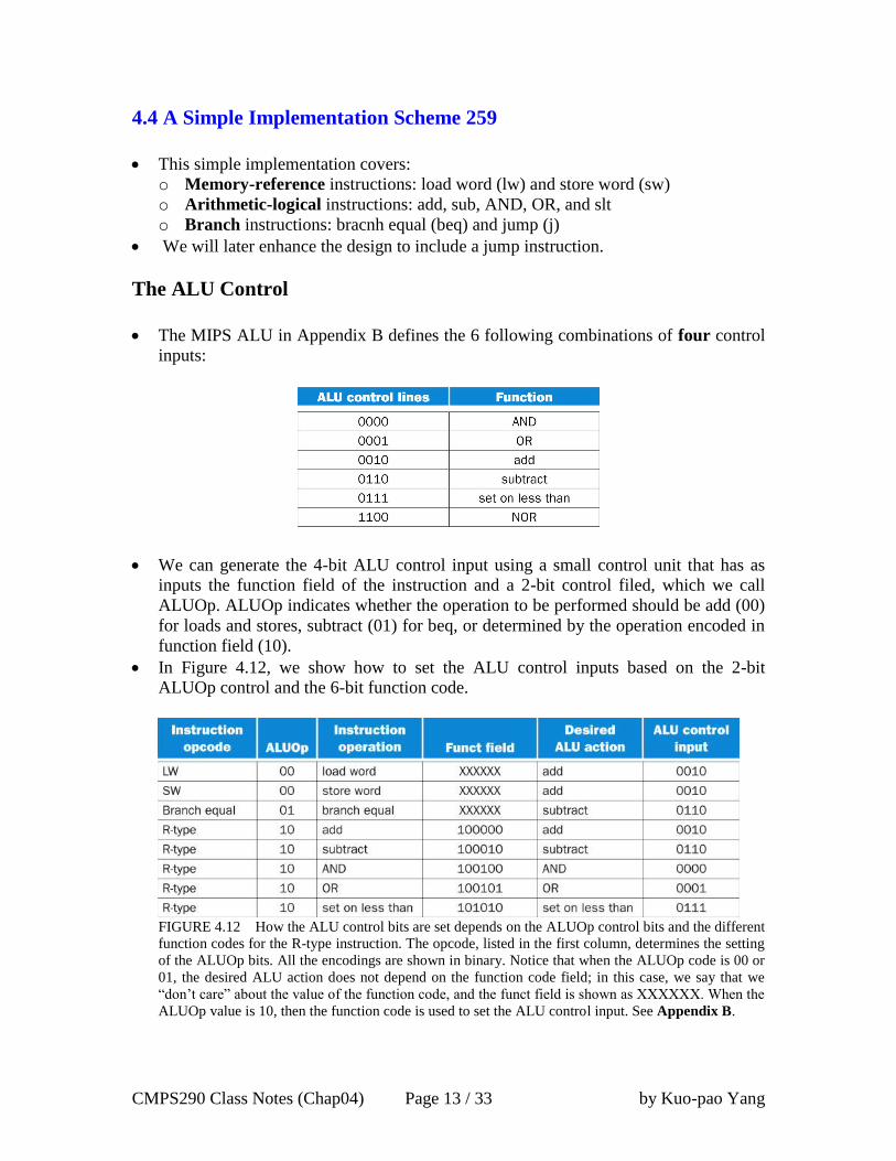
4.4 A Simple Implementation Scheme 259
This simple implementation covers:
o Memory-reference instructions: load word (lw) and store word (sw)
o Arithmetic-logical instructions: add, sub, AND, OR, and slt
o Branch instructions: bracnh equal (beq) and jump (j)
We will later enhance the design to include a jump instruction.
The ALU Control
The MIPS ALU in Appendix B defines the 6 following combinations of four control
inputs:
We can generate the 4-bit ALU control input using a small control unit that has as
inputs the function field of the instruction and a 2-bit control filed, which we call
ALUOp. ALUOp indicates whether the operation to be performed should be add (00)
for loads and stores, subtract (01) for beq, or determined by the operation encoded in
function field (10).
In Figure 4.12, we show how to set the ALU control inputs based on the 2-bit
ALUOp control and the 6-bit function code.
FIGURE 4.12 How the ALU control bits are set depends on the ALUOp control bits and the different
function codes for the R-type instruction. The opcode, listed in the first column, determines the setting
of the ALUOp bits. All the encodings are shown in binary. Notice that when the ALUOp code is 00 or
01, the desired ALU action does not depend on the function code field; in this case, we say that we
“don’t care” about the value of the function code, and the funct field is shown as XXXXXX. When the
ALUOp value is 10, then the function code is used to set the ALU control input. See Appendix B.

CMPS290 Class Notes (Chap04) Page 14 / 33 by Kuo-pao Yang
Designing the Main Control Unit
Figure 4.14 shows the formats of the three classes: R-type, load-store, and branch
FIGURE 4.14 The three instruction classes (R-type, load and store, and branch) use two different
instruction formats. The jump instructions use another format, which we will discuss shortly. (a)
Instruction format for R-format instructions, which all have an opcode of 0. These instructions have
three register operands: rs, rt, and rd. Fields rs and rt are sources, and rd is the destination. The ALU
function is in the funct field and is decoded by the ALU control design in the previous section. The R-
type instructions that we implement are add, sub, AND, OR, and slt. The shamt field is used only for
shifts; we will ignore it in this chapter. (b) Instruction format for load (opcode = 35ten) and store
(opcode = 43ten) instructions. The register rs is the base register that is added to the 16-bit address field
to form the memory address. For loads, rt is the destination register for the loaded value. For stores, rt
is the source register whose value should be stored into memory. (c) Instruction format for branch
equal (opcode =4). The registers rs and rt are the source registers that are compared for equality. The
16-bit address field is sign-extended, shifted, and added to the PC + 4 to compute the branch target
address.

CMPS290 Class Notes (Chap04) Page 15 / 33 by Kuo-pao Yang
Operation of the Datapath
Figure 4.17 shows the datapath with the control unit and the control signals. There are
7 single-bit control lines plus the 2-bit ALUOp control signal.
o Multiplexors: RegDst, ALUSrc, and MemtoReg
o Reads and Writes: RegWrite) and MemRead, MemWrite
o Determining branch: Branch
o ALU: 2-bit ALUOp.
FIGURE 4.17 The simple datapath with the control unit. The input to the control unit is the 6-bit
opcode field from the instruction. The outputs of the control unit consist of three 1-bit signals that are
used to control multiplexors (RegDst, ALUSrc, and MemtoReg), three signals for controlling reads and
writes in the register file and data memory (RegWrite, MemRead, and MemWrite), a 1-bit signal used
in determining whether to possibly branch (Branch), and a 2-bit control signal for the ALU (ALUOp).
An AND gate is used to combine the branch control signal and the Zero output from the ALU; the
AND gate output controls the selection of the next PC. Notice that PCSrc is now a derived signal,
rather than one coming directly from the control unit. Thus, we drop the signal name in subsequent
figures.

CMPS290 Class Notes (Chap04) Page 16 / 33 by Kuo-pao Yang
Datapath for R-type Instructions
Figure 4.19 shows the operation of the datapath for an R-type instruction
R-type format:
add $s1, $s2, $s3 # $s1 = $s2 + $s3
FIGURE 4.19 The datapath in operation for an R-type instruction, such as add $t1, $t2, $t3. The
control lines, datapath units, and connections that are active are highlighted.
0 rs rt rd shamt funct
31:26 5:0 25:21 20:16 15:11 10:6
0 18 19 17 0 32
31:26 5:0 25:21 20:16 15:11 10:6
CMPS290 Class Notes (Chap04) Page 17 / 33 by Kuo-pao Yang
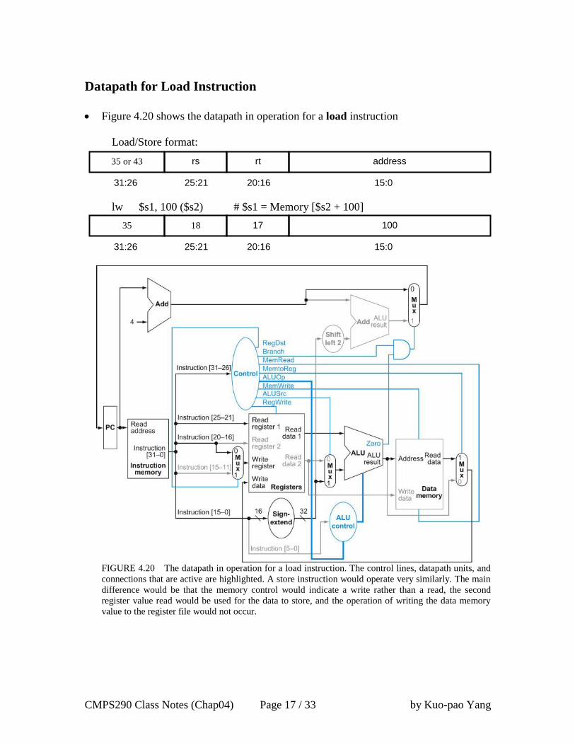
Datapath for Load Instruction
Figure 4.20 shows the datapath in operation for a load instruction
Load/Store format:
lw $s1, 100 ($s2) # $s1 = Memory [$s2 + 100]
FIGURE 4.20 The datapath in operation for a load instruction. The control lines, datapath units, and
connections that are active are highlighted. A store instruction would operate very similarly. The main
difference would be that the memory control would indicate a write rather than a read, the second
register value read would be used for the data to store, and the operation of writing the data memory
value to the register file would not occur.
35 or 43 rs rt address
31:26 25:21 20:16 15:0
35 18 17 100
31:26 25:21 20:16 15:0

CMPS290 Class Notes (Chap04) Page 18 / 33 by Kuo-pao Yang
Datapath for Branch-on-Equal Instruction
Figure 4.21 shows the datapath in operation for a branch-on-equal instruction
Branch on equal (beq) format:
beq $s1, $s2, 100 # if ($s1 == $s2) go to (PC+4) + 100
FIGURE 4.21 The datapath in operation for a branch-on-equal instruction. The control lines,
datapath units, and connections that are active are highlighted. After using the register file and ALU to
perform the compare, the Zero output is used to select the next program counter from between the two
candidates.
4 rs rt address
31:26 25:21 20:16 15:0
4 17 18 25
31:26 25:21 20:16 15:0

CMPS290 Class Notes (Chap04) Page 19 / 33 by Kuo-pao Yang
Datapath for Jump Instruction
Figure 4.24 shows the datapath are extended to handle the jump instruction, such as
Jump (j) format:
j 10000 # go to (PC+4) [31:28]: 10000
FIGURE 4.24 The simple control and datapath are extended to handle the jump instruction. An
additional multiplexor (at the upper right) is used to choose between the jump target and either the
branch target or the sequential instruction following this one. This multiplexor is controlled by the
jump control signal. The jump target address is obtained by shifting the lower 26 bits of the jump
instruction left 2 bits, effectively adding 00 as the low-order bits, and then concatenating the upper 4
bits of PC + 4 as the high-order bits, thus yielding a 32-bit address.
2 address
31:26 25:0
2 2500
31:26 25:0

CMPS290 Class Notes (Chap04) Page 20 / 33 by Kuo-pao Yang
4.5 An Overview of Pipelining 272
Pipelining is an implementation technique in which multiple instructions are
overlapped in execution. Today, pipelining is nearly universal.
Figure 4.25 shows the laundry analogy for pipelining
o If all the stages take about the same amount of time and there is enough work to
do, then the speed-up due to pipelining is equal to the number of stages in the
pipeline, in this case four: washing, drying, folding, and putting away.
o Four loads (4 loads):
Speed-up = (2 * 4) / (0.5 * 4 + 1.5) = 8.0 / 3.5 = 2.3
o Non-stop (n loads):
Speed-up = (2 * n) / (0.5 * n + 1.5) ≈ 4 (= number of stages)
FIGURE 4.25 The laundry analogy for pipelining. Ann, Brian, Cathy, and Don each have dirty
clothes to be washed, dried, folded, and put away. The washer, dryer, “folder,” and “storer” each take
30 minutes for their task. Sequential laundry takes 8 hours for 4 loads of wash, while pipelined laundry
takes just 3.5 hours. We show the pipeline stage of different loads over time by showing copies of the
four resources on this two-dimensional time line, but we really have just one of each resource.

CMPS290 Class Notes (Chap04) Page 21 / 33 by Kuo-pao Yang
MIPS Pipeline: Five stages, one step per stage
1. IF: Instruction fetch from memory
2. ID: Instruction decode & register read
3. EX: Execute operation or calculate address
4. MEM: Access memory operand
5. WB: Write result back to register
Example: Single-Cycle versus Pipelined Performance
o Compare pipelined datapath with single-cycle datapath. Assume time for stages is
100ps for register read or write
200ps for other stages
FIGURE 4.26 Total time for each instruction calculated from the time for each component. This
calculation assumes that the multiplexors, control unit, PC accesses, and sign extension unit have no
delay

CMPS290 Class Notes (Chap04) Page 22 / 33 by Kuo-pao Yang
FIGURE 4.27 Single-cycle, nonpipelined execution in top versus pipelined execution in bottom.
Both use the same hardware components, whose time is listed in Figure 4.26. In this case, we see a
fourfold speed-up on average time between instructions, from 800 ps down to 200 ps. Compare this
figure to Figure 4.25. For the laundry, we assumed all stages were equal. If the dryer were slowest,
then the dryer stage would set the stage time. The pipeline stage times of a computer are also limited
by the slowest resource, either the ALU operation or the memory access. We assume the write to the
register file occurs in the first half of the clock cycle and the read from the register file occurs in the
second half. We use this assumption throughout this chapter.
Pipeline Speedup
o If all stages are balanced: all stages take the same time
Time between instructionspipelined = Time between instructionsnonpipelined
Number of stages
o If not balanced, speedup is less
o In Figure 4.27, for three instructions: it’s 1,400 ps versus 2,400 ps
o We could extend Figure 4.27 to 1,000,003 instructions. The ratio of total
execution times for real programs on nonpipelined to pipelined processors is close
to the ratio of times between instructions:
2,400 + 1,000,000 * 800 = 8000,002,400ps = 800ps = 4.00
1,400 + 1,000,000 * 200 2000,001,400ps 200ps
Pipelining improves performance by increasing instruction throughput, as opposed
to decreasing the execution time of an individual instruction, but instruction
throughput is the import metric because real programs execute billions of instructions.
CMPS290 Class Notes (Chap04) Page 23 / 33 by Kuo-pao Yang
Designing Instruction Sets for Pipelining
MIPS instruction set, which was designed for pipelined execution.
1. All instructions are 32-bits
Easier to fetch and decode in one cycle
x86: 1- to 15-byte instructions
2. Few and regular instruction formats
Can decode and read registers in one step
3. Load/store addressing
Can calculate address in execute stage (3rd), access memory in 4th stage
x86: expand to an address stage, memory stage, then execute stage.
4. Alignment of memory operands
Memory access takes only one cycle
Designing Instruction Sets for Pipelining Pipeline Hazards
Three are situation in pipelining when the next instruction cannot execute in the
following clock cycle. These events are call hazards, and there are three different
types.
1. Structure Hazards
A required resource is busy
2. Data Hazards
Need to wait for previous instruction to complete its data read/write
3. Control Hazards
Deciding on control action depends on previous instruction

CMPS290 Class Notes (Chap04) Page 24 / 33 by Kuo-pao Yang
Structure Hazards
Structure hazards: the hardware cannot support the combination of instruction we
want to execute in the same clock cycle.
Suppose, that we had a single memory instead of two memories.
o Conflict for use of a resource
o Load/store requires data access memory
o Instruction fetch memory would have to stall for that cycle
Would cause a pipeline “bubble”
Hence, pipelined datapath require separate instruction/data memories. Without two
memories, our pipeline could have a structure hazard.

CMPS290 Class Notes (Chap04) Page 25 / 33 by Kuo-pao Yang
Data Hazards
Data hazards occur when the pipeline must be stalled because on step must wait for
another to complete.
Data hazards arise from the dependence of one instruction on an earlier one that is
still in the pipeline.
For example, suppose we have an add instruction followed immediately by a subtract
instruction that uses the sum ($s0)
add $s0, $t0, $t1 # $s0 = $t0 + $t1
sub $t2, $s0, $t3 # $t2 = $s0 + $t3
FIGURE 4.28 Graphical representation of the instruction pipeline, similar in spirit to the laundry
pipeline in Figure 4.25. Here we use symbols representing the physical resources with the
abbreviations for pipeline stages used throughout the chapter. The symbols for the five stages: IF for
the instruction fetch stage, with the box representing instruction memory; ID for the instruction
decode/register file read stage, with the drawing showing the register file being read; EX for the
execution stage, with the drawing representing the ALU; MEM for the memory access stage, with the
box representing data memory; and WB for the write-back stage, with the drawing showing the register
file being written. The shading indicates the element is used by the instruction. Hence, MEM has a
white background because add does not access the data memory. Shading on the right half of the
register file or memory means the element is read in that stage, and shading of the left half means it is
written in that stage. Hence the right half of ID is shaded in the second stage because the register file is
read, and the left half of WB is shaded in the fifth stage because the register file is written.
Example: Forwarding with Two instructions
o For the code sequence above, as soon as the ALU creates the sum for the add, we
can supply it as an input for the subtract.
o Adding extra hardware to retrieve the missing item early from the internal
resources is call forwarding or bypassing.
o Figure 4.29 show the connection to forward the value in $s0 after the execution
stage of the add instruction as input to the execution stage of the sub instruction

CMPS290 Class Notes (Chap04) Page 26 / 33 by Kuo-pao Yang
FIGURE 4.29 Graphical representation of forwarding. The connection shows the forwarding path
from the output of the EX stage of add to the input of the EX stage for sub, replacing the value from
register $s0 read in the second stage of sub.
Load-Use Data Hazard
o Can’t always avoid stalls by forwarding
If value not computed when needed
Can’t forward backward in time!
o We had to stall one stage for a load-use data hazard.
o Figure 4.30 show an important pipeline concept, officially called a pipeline stall,
but often given the nick name bubble.
FIGURE 4.30 We need a stall even with forwarding when an R-format instruction following a load
tries to use the data. Without the stall, the path from memory access stage output to execution stage
input would be going backward in time, which is impossible. This figure is actually a simplification,
since we cannot know until after the subtract instruction is fetched and decoded whether or not a stall
will be necessary. Section 4.7 shows the details of what really happens in the case of a hazard.

CMPS290 Class Notes (Chap04) Page 27 / 33 by Kuo-pao Yang
Example: Reordering Code to Avoid Pipeline Stalls
o Consider the following code segment in C:
a = b + e;
c = b + f;
o Here is the generated MIPS code for this segment, assuming all variable are in
memory and are addressable as offset from $t0:
lw $t1, 0($t0) # a = b + e;
lw $t2, 4($t0) # $t2 load-use data hazard: one stall
add $t3, $t1, $t2 #
sw $t3, 12($t0) #
lw $t4, 8($t0) # c = b + f;
add $t5, $t1, $t4 # $t4 load-use data hazard: one stall
sw $t5, 16($t0) #
o Moving up the third lw instruction (lw $t4, 8($t0)) to become the third
instruction eliminates both hazards:
lw $t1, 0($t0) #
lw $t2, 4($t0) #
lw $t4, 8($t0) # Moving up: eliminate both hazards
add $t3, $t1, $t2 #
sw $t3, 12($t0) #
add $t5, $t1, $t4 #
sw $t5, 16($t0) #
CMPS290 Class Notes (Chap04) Page 28 / 33 by Kuo-pao Yang
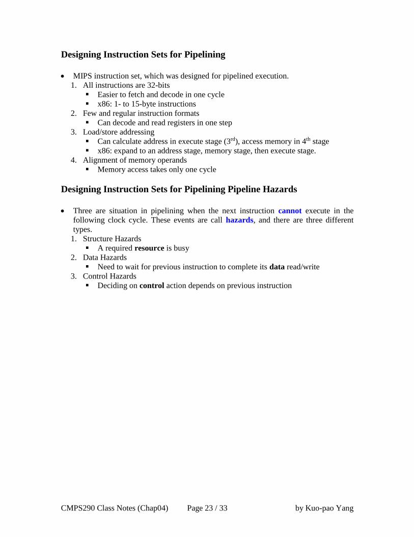
Control Hazards
Control hazard arising from the need to make a decision based on the results of one
instruction while other are executing.
Example: Performance of “Stall on Branch”
o Figure 4.31 shows stalling on every conditional branch as solution to control
hazards
FIGURE 4.31 Pipeline showing stalling on every conditional branch as solution to control hazards.
This example assumes the conditional branch is taken, and the instruction at the destination of the
branch is the OR instruction. There is a one-stage pipeline stall, or bubble, after the branch. In reality,
the process of creating a stall is slightly more complicated, as we will see in Section 4.8. The effect on
performance, however, is the same as would occur if a bubble were inserted.

CMPS290 Class Notes (Chap04) Page 29 / 33 by Kuo-pao Yang
Branch Prediction
o Computers do indeed use prediction to handle branches.
o One simple approach is to prediction always that branches will be untaken. When
you are right, the pipeline proceeds at full speed. Only when braches are taken
does the pipeline stall. Figure 4.32 show such an example.
FIGURE 4.32 Predicting that branches are not taken as a solution to control hazard. The top
drawing shows the pipeline when the branch is not taken. The bottom drawing shows the pipeline
when the branch is taken. As we noted in Figure 4.31, the insertion of a bubble in this fashion
simplifies what actually happens, at least during the first clock cycle immediately following the branch.
Section 4.8 will reveal the details.
More-Realistic Branch Prediction
o Static branch prediction
Based on typical branch behavior
Example: loop branches
At the bottom of loops are braches that jump back to the top of the loop.
Since they are likely to be taken and thy branch backward, we could
always predict taken for branches that jump to an earlier address.
o Dynamic branch prediction
Hardware measures actual branch behavior
record recent history of each branch
Assume future behavior will continue the trend
When wrong, stall while re-fetching, and update history

CMPS290 Class Notes (Chap04) Page 30 / 33 by Kuo-pao Yang
Pipeline Overview Summary
Pipelining is a technique that exploits parallelism among the instruction in a
sequential instruction stream.
It is fundamentally invisible to the programmer.
Pipelining improves performance by increasing instruction throughput
o Executes multiple instructions in parallel
o Each instruction has the same latency
Subject to hazards
o Structure, data, and control
Instruction set design affects complexity of pipeline implementation
CMPS290 Class Notes (Chap04) Page 31 / 33 by Kuo-pao Yang
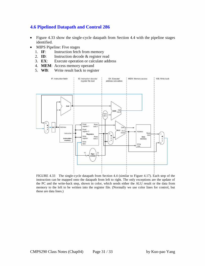
4.6 Pipelined Datapath and Control 286
Figure 4.33 show the single-cycle datapath from Section 4.4 with the pipeline stages
identified.
MIPS Pipeline: Five stages
1. IF: Instruction fetch from memory
2. ID: Instruction decode & register read
3. EX: Execute operation or calculate address
4. MEM: Access memory operand
5. WB: Write result back to register
FIGURE 4.33 The single-cycle datapath from Section 4.4 (similar to Figure 4.17). Each step of the
instruction can be mapped onto the datapath from left to right. The only exceptions are the update of
the PC and the write-back step, shown in color, which sends either the ALU result or the data from
memory to the left to be written into the register file. (Normally we use color lines for control, but
these are data lines.)

CMPS290 Class Notes (Chap04) Page 32 / 33 by Kuo-pao Yang
Figure 4.35 shows the pipeline version of the datapath in Figure 4.33
o Pipeline registers: Need registers between stages to hold information produced in
previous cycle
FIGURE 4.35 The pipelined version of the datapath in Figure 4.33. The pipeline registers, in color,
separate each pipeline stage. They are labeled by the stages that they separate; for example, the first is
labeled IF/ID because it separates the instruction fetch and instruction decode stages. The registers
must be wide enough to store all the data corresponding to the lines that go through them. For example,
the IF/ID register must be 64 bits wide, because it must hold both the 32-bit instruction fetched from
memory and the incremented 32-bit PC address. We will expand these registers over the course of this
chapter, but for now the other three pipeline registers contain 128, 97, and 64 bits, respectively.

CMPS290 Class Notes (Chap04) Page 33 / 33 by Kuo-pao Yang
4.15 Concluding Remarks 356
ISA influences design of datapath and control
Pipelining improves instruction throughput using parallelism
Hazards: structural, data, control
MIPS Pipeline: Five stages
1. IF: Instruction fetch from memory
2. ID: Instruction decode & register read
3. EX: Execute operation or calculate address
4. MEM: Access memory operand
5. WB: Write result back to register
FIGURE 4.24 The simple control and datapath are extended to handle the jump instruction. An
additional multiplexor (at the upper right) is used to choose between the jump target and either the
branch target or the sequential instruction following this one. This multiplexor is controlled by the
jump control signal. The jump target address is obtained by shifting the lower 26 bits of the jump
instruction left 2 bits, effectively adding 00 as the low-order bits, and then concatenating the upper 4
bits of PC + 4 as the high-order bits, thus yielding a 32-bit address.
FIGURE 4.17 The simple datapath with the control unit. The input to the control unit is the 6-bit
opcode field from the instruction. The outputs of the control unit consist of three 1-bit signals that are
used to control multiplexors (RegDst, ALUSrc, and MemtoReg), three signals for controlling reads and
writes in the register file and data memory (RegWrite, MemRead, and MemWrite), a 1-bit signal used
in determining whether to possibly branch (Branch), and a 2-bit control signal for the ALU (ALUOp).
An AND gate is used to combine the branch control signal and the Zero output from the ALU; the
AND gate output controls the selection of the next PC. Notice that PCSrc is now a derived signal,
rather than one coming directly from the control unit. Thus, we drop the signal name in subsequent
figures.