chapter 4 improved psm dc-dc buck...
TRANSCRIPT

97
CHAPTER 4
IMPROVED PSM DC-DC BUCK CONVERTER
Ripple content on the output voltage is an important performance
parameter in switch mode power supplies. The load ripple voltage depends
inversely on the switching frequency, and hence it should be as high as
possible to reduce the ripple content. This also helps to reduce the component
size and weight as well.
Higher ripple content is a demerit in PSM buck converter and
prevents the successful use of the converter in many applications in spite of
its other advantages.
Ripple content in output voltage is mainly due to charging and
discharging current through the capacitor, which can be considered to be due
entirely to inductor current ripple. The charging current raises and lowers the
quantity of charge on the capacitor thus increasing or decreasing the level of
the voltage when ESR of capacitor is not considered. When ESR of a
capacitor is not negligible, then the voltage ripple is almost entirely the
voltage drop across ESR due to capacitor current, which is wholly the
inductor ripple current, especially when ESR is much less than the load
resistance, which is mostly the case.
4.1 RIPPLE IN DC-DC BUCK CONVERTERS
For a DC-DC buck converter operating under CCM output voltage
ripple equation can be derived as shown below.

98
The output voltage vO includes the DC component VO and AC
component VO. This voltage vO is produced by the inductor current iL
flowing through the load R and output capacitor C. The converter is so
designed that the output capacitor provides a very low impedance path for
inductor current ripple at regulator switching frequency and hence almost all
of the inductor ripple current will flow through the output capacitor, C and the
DC component, which is the average inductor current, flows through the load.
Inductor current iL = I L avg + iL (4.1)
Output voltage v0 = V0 + v0 (4.2)
Inductor current DC component I Lavg = I0 = V/R (4.3)
Inductor current ripple can be derived from Figure 4.1.
Figure 4.1 Inductor current in buck converter
Let the current rise during ON time from a minimum value to a maximum value.
Let
Ip = maximum value of inductor current (4.4)
99
Iv = minimum value of inductor current (4.5)
During ON time
onin
vp TL
VVII 0 (4.6)
vp III (4.7)
onin
L TL
VVI 0 (4.8)
Similarly during OFF time
offL TL
VI 0 (4.9)
At steady state
0VV
D in (4.10)
From Equations (4.8) to (4.10) we get the inductor ripple current
sL TL
VDI 01 (4.11)
The output capacitor charging and discharging current is equal to
the inductor ripple current.
Considering linearly rising and falling current flowing in the output
capacitor.
iC rises during Ton: },0{ onTt
onL
LC T
tI
Ii
2 (4.12)
100
iC falls during Toff: },0{ offTt
offL
LC T
tIIi2
(4.13)
where IL is the total inductor current ripple.
Integrating Equations (4.12) and (4.13)
ttt
CI
CttI
CtIdttI
C on
L
onL
Lt
C
22
01 222
).(1 (4.14)
off
L
offL
Lt
C ttt
CI
CttI
CtIdttI
C
22
02 222
).(1 (4.15)
For the instant at which maximum point occurs:
Differentiating Equations (4.14) and (4.15)
02 on
LL
ttII (4.16)
Therefore2ontt
02 offt
tLILI
(4.17)
Therefore2offt
t

101
Substituting in Equations (4.16) and (4.17) and manipulating, the
voltage peak to peak ripple can be got as the difference between the
maximum and minimum values and is equal to:
CTI
TTCI
CTI
CTI
V sLoffon
LonLoffL
8888 (4.18)
Substituting Equation (4.11) the ripple voltage is given by
LCTVD
V s
81 2
0
(4.19)
Normalising with V0
Voltage ripple
LCTD
VVr s
81 2
0 (4.20)
LCfD
281 (4.21)
Here the effect of ESR is not considered. The ESR appears like a
resistor in series with the capacitor as shown in Figure 4.2. The ac inductor
current ripple no longer flows through C alone, but a combination of C and a
resistor in series, RESR.
Figure 4.2 Equivalent circuit of capacitor with ESR
C RESR

102
The drop due to this element is
ESRLESR RIV (4.22)
onin
L TL
VVI 0 (4.23)
ESRsin
ESR RDTL
VVV 0 (4.24)
sL TL
VDI 01 (4.25)
ESRs
ESR RLf
DVV 1
0 (4.26)
4.2 FACTORS AFFECTING RIPPLE IN BUCK CONVERTERS
For inductor-based switching regulators that include a buck
converter with an output LC filter, the factors that affect output voltage ripple
include switching frequency, duty cycle, output capacitor value and its ESR.
From Equation (4.21) it can be stated that the ripple depends on the
duty cycle D, switching frequency f, inductance L, and capacitance C when
ESR is negligible. When ESR of the filter capacitor is considerable then the
ripple would be mostly due to the drop across ESR and the ripple due to
capacitance would be much smaller in comparison with the dominating ESR
ripple (Abraham Pressman et al 2009).
The Effect of the parameters f, D, L, C on a DC/DC buck
Converter Output Voltage Ripple is shown in Figures 4.3 to 4.5, at various
frequencies (Analogic Tech Application note AN-215 2008) .
The ripple decreases as L is increased as seen from Figure 4.4. The
ripple decreases as D is increased as seen from Figure 4.5. The load current

103
does not affect the ripple in the case of buck converter under continuous
conduction mode as seen from Equation (4.21). The ripple decreases when
frequency is increased as seen from all the diagrams.
Figure 4.3 Output voltage ripple Vs frequency with C as parameter
The ripple decreases as C is increased as seen.
Figure 4.4 Output voltage ripple Vs frequency with L as parameter
104
Figure 4.5 Output voltage ripple Vs frequency with D as parameter
When ripple depends on ESR then based on the ripple requirement
the capacitor can be selected with a required ESR. The ESR if not known can
be roughly calculated from the capacitor value as the product of ESR and C is
generally in the range 50X10-6 to 80X10-6. Then minimising the inductor
current ripple would directly control voltage drop across ESR and hence the
output voltage ripple. It is also to be noted that the peak-to-peak value of
ripple voltage increases with increase in input voltage.
In the case of DCM the voltage ripple is given by
DR
LfCfDCR
LCRfV
Vr
L
s
sLLs 1
2112
132
0
0
(4.27)
Ripple decreases with the increase of RL or the decrease of input
voltage, Vi that would increase D. The minimum inductance to guarantee the
lowest ripple is the critical inductance of CCM under the highest input
voltage and the maximum load (Liu Shulin 44). With ESR considered, the
ripple, as it depends on the inductor current ripple, would be lower if the latter
is controlled.

105
Figure 4.6 Inductor current in DCM
The current ripple and hence the voltage ripple can be calculated
from Figure 4.6. The current rises from zero to Ip in D1Ts and falls to zero in
D2Ts. The portion of on time over which current is above the average value is
t1 and that during off time is t2.
Then
t1/(D1.Ts)=(Ip-Io)/Ip (4.28)
t2/(D2.Ts)=(Ip-Io)/Ip (4.29)
Since the charge increase is given by the product of voltage ripple
and C,
V0= 2(Ip-Io)(t1+t2)/C (4.30)
= (Ip-Io)(Ip-Io) (D1+D2)Ts/Ip C (4.31)
The extinction time Tx is given by
Tx = (D1+D2 )Ts = d1Vin / fsV0 (4.32)
If the ESR is considerable the ripple voltage would be the product
of ripple current and ESR and hence the ripple can be reduced by selecting a
low ESR capacitor or reduce the peak value of inductor current.

106
In the case of pulse skipping modulated buck converter under
continuous conduction mode the ripple is given by (Luo Ping et al 2006):
(4.33)
The Equation (4.33) does not consider ESR of filter capacitor. In a
practical converter with ESR considered the ripple could be determined from
inductor current ripple as ESR ripple usually dominates over the ripple due to
capacitance alone.
Figure 4.7 Inductor current and output voltage in PSM converter under CCM
In a typical PSM converter with p pulses applied under CCM the
current would rise to Ip from Iv as shown in Figure 4.7. Let in qTs seconds
the current drops to Iv.
Then during the charging cycle, consisting of p pulses, net rise in
current through the inductor can be expressed as
pLf
VVDIps
inpc
01
(4.34)
qpqDLC
TVV
r s1
2
0
0 18
0.2026 0.2028 0.203 0.2032 0.2034 0.2036 0.2038 0.204Time (s)
4
4.5
5
5.5
6
Ip
Iv
v0
Inductor current iL in A
Output voltage across capacitor in V
[0.202689 , 5.62476]
[0.20285 , 4.38816]
[0.203357 , 5.09381]
[0.203506 , 4.90955]

107
sin
pc pTL
VVDIp 01
(4.35)
In q cycles the fall in current would be by the same value at steady
state and given by
sqTL
VI 0
(4.36)
With
Ta = (p+q) Ts (4.37)
From Equations (4.35) to (4.37) Peak-to-peak inductor current
ripple is given by
L
VVD
V
TI ina
01
01
(4.38)
In a pulse-skipping converter under CCM, D1 is slightly greater
than V0/Vin to effect regulation of v0. If capacitance is large then the ripple
current would flow through the capacitor entirely and average current would
flow through the load. The average current from Figure 4.8 can be
determined as follows:
Figure 4.8 Inductor current in PSM converter under CCM
0.4996 0.4998 0.5Time (s)
2
3
4
5
6
7
8
Imax
IminpTs qTs
i L(A
)
108
The approximate total area
= minmaxmin 21 IIqTpTIqTpT ssss (4.39)
Therefore
)I(I21
II minmaxminavg (4.40)
sin pTL
VVD 01minmax II (4.41)
min01
2IpT
LVVD
I sin
avg (4.42)
min01
2Ip
LfVVD
Is
inavg (4.43)
The average current flows through load, and equals
min010
2Ip
LfVVD
RV
Is
inavg (4.44)
Equation (4.44) can be rearranged and can be used to find out the
inductance for a particular mode of operation. Assuming the charging cycle
has number of pulses greater than one with Imin not equal to zero, for an
inductor current peak-to-peak ripple of I,
ILfVV
D sin
011
(4.45)
The ripple voltage V0 is due to the charging capacitor current
which is equal to the inductor current ripple for a large capacitor and the

109
ripple can be calculated as the charge increase in capacitor divided by the
capacitance.
CQV0 (4.46)
From area under the charging current pulse the charge increase can
be written as
pItQ21 (4.47)
where
sTqpt21 (4.48)
From Equations (4.35), (4.47) and (4.48)
sin
s pTL
VVDTqpV
221
21 01
0 (4.49)
20
1
0
0
8
1
s
in
LCf
VVD
qppVV
r (4.50)
In a converter that uses a capacitor with considerable ESR the
ripple is given by
CtRIV ESR 20 (4.51)
First part of the equation represents the drop across RESR due to
charging current through the ESR, which is equal to inductor current ripple

110
when the capacitor is large enough. It is the peak-to-peak value of the ripple
current that is used.
ESR can be estimated from the ESR and C product, which is
usually in the range 50X10-6 to 80X10-6. Using the average value of 65X10-6
for a capacitor of 470 F ESR is 0.138 and the second part inside the braces of
Equation (4.51) is roughly 0.027. Hence the ESR effect dominates over that
of capacitance in ripple voltage normally. Hence the factors that affect output
voltage ripple include inductor current ripple, ESR, frequency fs, L, D1 and C
with ESR and inductor current ripple significant ones.
4.3 IMPROVED PSM DC-DC BUCK CONVERTER
Output voltage ripple in PSM converter, can be decreased by
decreasing the inductor current ripple. The Inductor Current Ripple (LIR) can
be controlled to be within a desired fraction of the load current by suitably
controlling the switch. In the PSM converter proposed the ripple current is
controlled to be within a desired maximum and minimum through pulse
skipping modulation.
Inductor current ripple LIR = Imax-Imin
In the PSM buck converter the inductor current is sensed and the
pulses are applied to the switch till the current reaches Imax. After the current
reaches Imax the pulses are skipped till the current reaches Imin. The
schematic is shown in Figure 4.9.
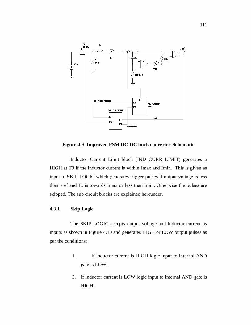
111
Figure 4.9 Improved PSM DC-DC buck converter-Schematic
Inductor Current Limit block (IND CURR LIMIT) generates a
HIGH at T3 if the inductor current is within Imax and Imin. This is given as
input to SKIP LOGIC which generates trigger pulses if output voltage is less
than vref and IL is towards Imax or less than Imin. Otherwise the pulses are
skipped. The sub circuit blocks are explained hereunder.
4.3.1 Skip Logic
The SKIP LOGIC accepts output voltage and inductor current as
inputs as shown in Figure 4.10 and generates HIGH or LOW output pulses as
per the conditions:
1. If inductor current is HIGH logic input to internal AND
gate is LOW.
2. If inductor current is LOW logic input to internal AND gate is
HIGH.

112
3. If output voltage is less than reference voltage, logic input to
internal D Flip-Flop is HIGH.
4. When input to D Flip-Flop is LOW skipping cycle starts and
pulses are blocked and not applied to switch.
5. When input to D Flip-Flop is HIGH the charging cycle starts
and pulses are applied to the switch.
6. During this period if Inductor current is high the input to
internal AND gate is low and hence the pulses are blocked,
limiting the inductor current.
In the schematic the logic is a sub circuit and implemented with
comparators, logic gates and D flip-flop, along with inductor current and
output voltage sensors.
Figure 4.10 Skip logic sub circuit
Q
Q
D
T3T1
&
Vref
CLK

113
4.3.2 Inductor Current Limit
The block accepts input from Inductor current and the skip logic
block T2 that is the result of whether v0 is less than Vref as shown in
Figure 4.11. Inductor current sensor output is at T1 and T2 is from skip logic.
1. If IL is greater than Imax the Flip Flop is reset and T3 goes
LOW.
2. If IL is less than Imin and if v0 is less than Vref the Flip Flop is
set and T3 goes HIGH.
Figure 4.11 Inductor current limit sub circuit
Even if Imax and Imin are carefully set it is seen that the inductor
current overshoots the limits due to delay of the circuit elements as can be
seen from the results
S
R
Q
Q
T1
T2
T3
&
Imax
Imin

114
Typical inductor current and output voltage waveforms are as
shown in Figure 4.12.
Figure 4.12 Typical output voltage and inductor current waveforms - improved converter
Inductor current dips to a low value when pulses are skipped to
regulate the voltage as seen in Figure 4.12. Corresponding CLK and pulses
applied to switch are shown in Figure 4.13.
Figure 4.13 CLK and pulses applied to switch
0.007 0.008 0.009Time (s)
0
2
4
6
8
0
0.2
0.4
0.6
0.8
1
Applied Pulses
0.007 0.008 0.009Time (s)
0
0.2
0.4
0.6
0.8
1
CLK

115
Simulation of the converter circuit is carried out with PSIM. The
following parameters are considered for simulation.
Table 4.1 Parameter values considered for the improved PSM buck converter
Parameter Value Unit Vin 12 to 35 VV0 5 VI0 1 AL 156 HRESR 50RDSON 0.05vd 0.4 VTs 25 SLIR 30% -Vref 5 V
Output voltage and current waveforms at nominal input voltage of
12V are shown in Figure 4.14. Initial capacitor voltage is 0V and the voltage
reached 5V in about 0.04S at 12V input with 1A load as shown in
Figure 4.15.
Figure 4.14 Output voltage and load current waveforms at nominal input voltage of 12V
4.8
5
5.2
0.024 0.026 0.028 0.03Time (s)
0.96
0.98
1
1.02
1.04

116
Figure 4.15 Starting output and capacitor voltages and inductor current – at 12V input voltage
The input voltage is increased from 12V to 20V and the output and
input voltage waveforms are shown in Figure 4.16. There is an increase in
ripple from 0.015V p-p to 0.0178V p-p as the input voltage increased from
12V to 20V.
Figure 4.16 Output voltage and applied input voltage – response to a step increase in input voltage from 12V to 20V
012345
Output Voltage in V
012345
Cap Voltage in V
0 0.01 0.02 0.03 0.04Time (s)
0
0.4
0.8
1.2
Ind Current i A
4.8
5
5.2
5.4
[0.0304738 , 5.00008]
[0.0307563 , 4.985]
[0.0328479 , 5.0003]
[0.0328826 , 4.9825]
0.03 0.031 0.032 0.033 0.034Time (s)
10
12
14
16
18
20

117
The load current is varied from 1A to 500mA and the output
voltage waveform is plotted as shown in Figure 4.17. The voltage ripple at
500mA is 0.019V p-p and at 1A the ripple is 0.018V p-p. The output voltage
inductor current portrait is shown in Figure 4.18. It is seen that there is
periodic inductor current discontinuity to regulate the voltage to 5V through
pulse skipping.
Figure 4.17 Output voltage and load current – response to a step decrease in load current from 1A to 0.5 A
Figure 4.18 Output voltage – Inductor current portrait. Average inductor current or load current is 1A. Pulses skipped result in periodical inductor current discontinuity
4.9
5
5.1
[0.0300471 , 4.98222]
[0.0303266 , 5.00019][0.026135 , 5.01244]
[0.0262308 , 4.99349]
0.026 0.028 0.03Time (s)
0.2
0.4
0.6
0.8
1
1.2
0 0.5 1 1.5I4
4.975
4.98
4.985
4.99
4.995
5
5.005
Inductor Current in A

118
4.4 APPLICATIONS OF PSM DC-DC BUCK CONVERTER
4.4.1 Regulated Power Supply
Most electronic circuits require constant DC voltage for their
operation. Supply voltage requirement is usually 3.3V, 5V, 6V, 9V or higher
at times. With line and battery voltages remaining the same buck converters
find increasing application in this area. Power supplies must be of low ripple,
low weight and volume, good efficiency, good response to load current and
supply voltage changes and input EMI performance. Switch mode power
supplies that use switching converters operate at high efficiency with
conversion ratio not an impediment mostly. They are light and the volume is
also lower as they work at high frequencies with the ripple component
slightly on the higher side.
The basic PSM converter has considerably higher ripple compared
to PWM converters and the improved converter discussed in section 4.3 is
considered. Linear regulators operate with very low ripple and efficiency
would not be a problem if conversion ratio were closer to unity. It is therefore
possible to combine the merits of switch mode converters and linear
regulators by cascading them (Scot Lester 2006) so that the demerit of PSM is
taken care of by low ripple conversion of linear regulator.
A hybrid power supply is proposed where the ripple performance
of a linear regulator is combined with PSM regulator’s high efficiency, low
weight and volume by cascading the two stages as shown in Figure 4.19.

119
Figure 4.19 Cascaded PSM and linear arrangement for power supply – Block schematic
PSM regulator with nominal input voltage of 12V and output
voltage of 7.5V is designed and cascaded with a linear regulator that can
convert a 7.5V to 5V. A three terminal IC 7805 was used but a series pass
PNP transistor or a MOSFET that can drop a voltage of I RDSON can be used
for lower input voltages that can further minimise the second stage
conversion ratio, which would improve the efficiency.
4.4.1.1 Simulation
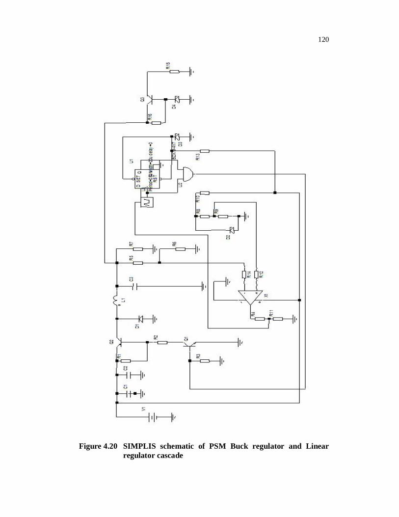
The circuit schematic is shown in Fig.4.20, which was simulated
using SIMPLIS and the output voltage waveform of the first stage is shown in
Figure 4.21 along with the reference voltage. Input was at 12V and the
reference was at 7.5V with the help of a zener diode and potential divider
with a preset for adjusting the reference voltage. Unregulated input voltage is
used with a limiter for feeding the reference circuit. A 40kHz clock with a D
flip flop and AND gate is used for pulse skipping modulation. Power
Transistor gate is driven by a general purpose switching transistor 2N2222.
The reference voltage is compared with actual output voltage with a help of
LM741. The output voltage of the PSM converter stage had a ripple of 4%.
Switchmode Circuit
Linear Reg Circuit
V0Vin
120
Figure 4.20 SIMPLIS schematic of PSM Buck regulator and Linear regulator cascade
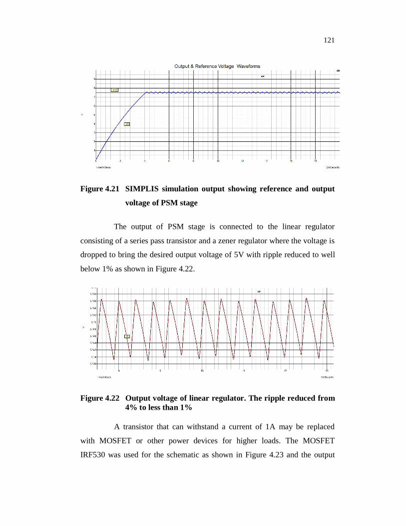
121
Figure 4.21 SIMPLIS simulation output showing reference and output
voltage of PSM stage
The output of PSM stage is connected to the linear regulator
consisting of a series pass transistor and a zener regulator where the voltage is
dropped to bring the desired output voltage of 5V with ripple reduced to well
below 1% as shown in Figure 4.22.
Figure 4.22 Output voltage of linear regulator. The ripple reduced from 4% to less than 1%
A transistor that can withstand a current of 1A may be replaced
with MOSFET or other power devices for higher loads. The MOSFET
IRF530 was used for the schematic as shown in Figure 4.23 and the output

122
waveforms of the two stages and the clock and gate pulses are shown in
Figure 4.24.
Figure 4.23 Schematic of PSM converter with MOSFET IRF530 cascaded with linear regulator
Figure 4.24 Simulation output showing voltage output of PSM converter, linear regulator and Inductor current along with clock and applied pulses
4.4.1.2 Experimental evaluation
The PSM-LDO buck regulator is constructed by cascading a PSM regulator designed to operate at 40 kHz with a nominal input voltage of 12V and output voltage of 7.5V. The linear regulator is simplified to be LM7805 that can regulate and provide a 5V output. The linear IC for regulation
BZX79-4V7D3
R16
R13
U3Period=25u width=20u delay=0
R11
R14
R12X1
D2
R9
D1R7R5C3
C1 C2
R3
R6
L1
R8
V1
R10
U2
R4
LS74U1D Q
QNRST
SET
BZX79-6V2D4
Q3
R15
E1
1
IRF530Q1
E1-CP
I(L1-
P)
/A
Y2
-0
0.5
1
1.5
2
2.5
3
U1-CLK
Time/mSecs 500uSecs/div
2.5 3 3.5 4 4.5 5 5.5 6
V
Y1
0
1
2
3
4
5
6
7
8

123
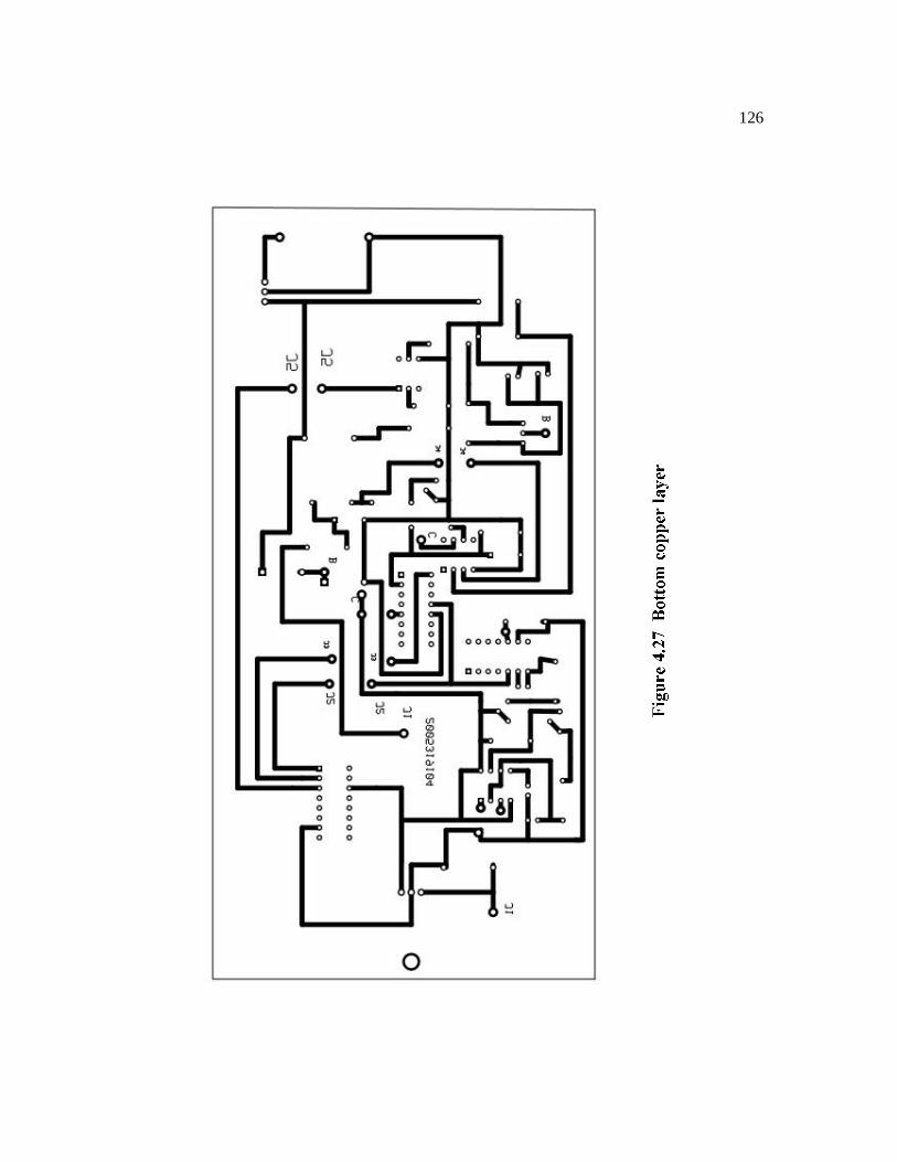
requires headroom of about 2.5V above the output voltage, which is provided by setting the reference voltage of first stage to be 7.5V. It is possible to design using other LDOs, which require much lesser headroom and may offer better ripple performance. The PCB is designed using ExpressPCB after schematic is done using ExpressSCH by linking the schematic to PC Board. The actual schematic, PC Board component layout and bottom copper track layout are shown in Figures 4.25 to 4.27.
The converter uses a transistor ZTX751 that can withstand a current of 1A. Output voltage signal of the converter is across R6, which is compared with the reference voltage generated by the zener reference circuit. Preset R10 is used to adjust the reference voltage. The reference voltage is set to be 3.75V with R5=R6.
The comparator output being HIGH or LOW is fed to the D flip-flop. If the D input to the flip-flop IC7475 is high, the next pulse generated by the clock will be passed. If D input to the flip-flop is low, the next pulse generated by the clock is blocked.
The clock generator generates a 40 kHz square wave using an IC555. It is also possible to use IC4060 with a 640kHz resonator or a relaxation oscillator using 7414 Schmitt NAND with suitable R&C. Eventhough IC4060 is stable with a resonator, oscillator with LM555 was found to be reliable and hence was preferred.
The output square wave is given as input to the 74LS123 which is a dual retriggerable monostable multivibrator, used here mainly to adjust the duty cycle with the help of the preset R15. AND gate passes the clock if D flip flop output is high and the transistor is switched on if the optocoupler output transistor is ON. The transistor can readily be replaced with a MOSFET, which can be driven by the optocoupler 4N25.

124

125
126

127
4.4.2 Chaos Free Operation with Mode Hopping
Power consumption is an important issue in systems that use
energy limited sources like battery or renewable energy especially when they
are mobile or remote. These applications demand high efficiency over wide
load range. A popular method to increase the efficiency over wide load range
is the hybrid mode composed of PWM and PFM (Jinwell Xiao et al 2004 and
Biranchinath Sahu and Gabriel Rincon-Mora 2005). Since PFM has demerits
such as varying frequency making the filter design difficult PWM/PSM dual
mode is being applied recently for sleep/wait mode in portable applications
(Ping Luo et al 2009).
In a dual mode converter during moderate to heavy load operation
PWM mode is adopted and during light loads operation is switched to PSM
mode. Pulse skipping mode maintains high efficiency during standby and idle
times in portable equipment thus increasing overall battery life and time
before next charging operation. The condition of light load is detected and
operation is switched to PSM mode with a suitable sensing and logic
circuitry. In a Programmable PWM/PSM control a logic circuit involves an
AND gate which blocks or passes PWM pulses or the circuit can select one of
the two signals available always.
Studies have shown that PWM dc-dc converters might exhibit
nonlinear phenomena under certain conditions (Chakrobarthy et al 1996,
Fossas and Olivar 1996). In a simple second order idealised buck converter
with voltage mode PWM control, subharmonics and chaos were uncovered
with evidence for a period doubling route to chaos. DC input voltage was the
parameter which when varied resulted in exhibition of bifurcation and in chaotic
operation for further increase in parameter value (Deane and Hamill 1990).
In a PWM converter the period doubling might occur at higher
values of input voltage and the converter would operate in discontinuous

128
conduction mode mostly. Since it has been shown that PSM converter under
discontinuous mode do not exhibit chaos, the operating mode can be switched
to PSM from PWM using a suitable logic. The scheme in Figure 4.28 is used
to verify that a converter which tends to be chaotic under PWM mode, operates free of chaos with PSM discontinuous mode.
In the scheme the PWM block accepts output voltage as the input and generates PWM signals at T5. PSM block accepts output voltage as input and generates PSM signal at its output T2. PWM/PSM SELECT block accepts PWM signal as input at T2 and PSM signal as input at T3. The SELECT block also accepts input voltage signal as input at T5. Mode change occurs when input voltage is compared to be greater than the set voltage beyond which the converter exhibits chaos. The selector switch connects either PWM or PSM output to power switch gate terminal and hence mode hopping occurs at the set voltage to avoid chaotic operation.
Figure 4.28 PWM/PSM Hybrid mode with mode select for chaos free operation
V
Vo
A B
V
Vin
V
T5
T3
T2
PWM/PSMSELECT
T2T1PSM
T5T4
T3
T2
PWM

129
Figure 4.29 Output voltage near transition to PSM from PWM at Vin of 30V
Figure 4.30 Bifurcation diagram - chaotic to non-chaotic transition at Vin = 30V
In the scheme suggested in Figure 4.28 PWM block generates
PWM pulses and PSM block generates PSM pulses. SELECT block switches
between PWM and PSM based on the input voltage and the knowledge of the
probable input voltage at which the converter may exhibit chaotic
phenomena. When input voltage goes higher than that critical value the mode
is hopped to PSM.
29.80 29.90 30.00 30.10 30.20V25
4.00
4.50
5.00
5.50
6.00
25.00 30.00 35.00V25
4.00
4.50
5.00
5.50
6.00
6.50

130
Figure 4.29 is a portion of the plot between output voltage and
input voltage as input voltage is varied from 24V to 34V The output voltage
waveform near 30 volt is erratic as seen from Fig.4.29 and as seen in the
bifurcation diagram in Figure 4.30, the converter is chaotic beyond at least
24V. The scheme is designed to switch over to PSM mode at 30V with the
help of a selector switch, which senses the input voltage and changes the
mode from PWM to PSM without any change in other parameters.
It is seen that the output voltage quickly regains order and as seen
in the bifurcation diagram the output voltage is periodic and nonchaotic. The
ripple on the output voltage is much less compared to that when the converter
is working in PWM mode nearby to an input voltage of 30V before mode
hopping.
4.5 CONCLUSION
It was found that the ripple depends on the ESR in cases where the
ESR is not negligible and by limiting the inductor current ripple in such cases
the ripple can be minimised. An improved PSM DC/DC converter with
inductor current limit with output voltage regulation was discussed. DC/DC
converters are widely used in power suppies. Low ripple, weight and volume
are among the important requirements of power supplies. Since PSM
converters operate in general with high ripple a PSM - Linear converter
cascade arrangement was discussed in this chapter with better ripple
performance. The circuit design along with PCB layout was presented.
The PSM mode is generally combined with PWM mode and dual
mode operation is usual. In such converters a mode hopping technique to
avoid chaotic operation of PWM converter was discussed to switch to PSM
forced discontinuous mode that is chaos free.